US10862185B2 - Integrated circuit with capacitor in different layer than transmission line - Google Patents
Integrated circuit with capacitor in different layer than transmission line Download PDFInfo
- Publication number
- US10862185B2 US10862185B2 US16/107,377 US201816107377A US10862185B2 US 10862185 B2 US10862185 B2 US 10862185B2 US 201816107377 A US201816107377 A US 201816107377A US 10862185 B2 US10862185 B2 US 10862185B2
- Authority
- US
- United States
- Prior art keywords
- integrated circuit
- plate
- capacitor
- transmission line
- disposed
- Prior art date
- Legal status (The legal status is an assumption and is not a legal conclusion. Google has not performed a legal analysis and makes no representation as to the accuracy of the status listed.)
- Active, expires
Links
Images


Classifications
-
- H—ELECTRICITY
- H01—ELECTRIC ELEMENTS
- H01P—WAVEGUIDES; RESONATORS, LINES, OR OTHER DEVICES OF THE WAVEGUIDE TYPE
- H01P3/00—Waveguides; Transmission lines of the waveguide type
- H01P3/02—Waveguides; Transmission lines of the waveguide type with two longitudinal conductors
- H01P3/08—Microstrips; Strip lines
-
- H—ELECTRICITY
- H10—SEMICONDUCTOR DEVICES; ELECTRIC SOLID-STATE DEVICES NOT OTHERWISE PROVIDED FOR
- H10D—INORGANIC ELECTRIC SEMICONDUCTOR DEVICES
- H10D84/00—Integrated devices formed in or on semiconductor substrates that comprise only semiconducting layers, e.g. on Si wafers or on GaAs-on-Si wafers
- H10D84/201—Integrated devices formed in or on semiconductor substrates that comprise only semiconducting layers, e.g. on Si wafers or on GaAs-on-Si wafers characterised by the integration of only components covered by H10D1/00 or H10D8/00, e.g. RLC circuits
- H10D84/204—Integrated devices formed in or on semiconductor substrates that comprise only semiconducting layers, e.g. on Si wafers or on GaAs-on-Si wafers characterised by the integration of only components covered by H10D1/00 or H10D8/00, e.g. RLC circuits of combinations of diodes or capacitors or resistors
- H10D84/212—Integrated devices formed in or on semiconductor substrates that comprise only semiconducting layers, e.g. on Si wafers or on GaAs-on-Si wafers characterised by the integration of only components covered by H10D1/00 or H10D8/00, e.g. RLC circuits of combinations of diodes or capacitors or resistors of only capacitors
-
- H—ELECTRICITY
- H01—ELECTRIC ELEMENTS
- H01L—SEMICONDUCTOR DEVICES NOT COVERED BY CLASS H10
- H01L23/00—Details of semiconductor or other solid state devices
- H01L23/52—Arrangements for conducting electric current within the device in operation from one component to another, i.e. interconnections, e.g. wires, lead frames
- H01L23/522—Arrangements for conducting electric current within the device in operation from one component to another, i.e. interconnections, e.g. wires, lead frames including external interconnections consisting of a multilayer structure of conductive and insulating layers inseparably formed on the semiconductor body
- H01L23/5222—Capacitive arrangements or effects of, or between wiring layers
- H01L23/5223—Capacitor integral with wiring layers
-
- H—ELECTRICITY
- H01—ELECTRIC ELEMENTS
- H01L—SEMICONDUCTOR DEVICES NOT COVERED BY CLASS H10
- H01L23/00—Details of semiconductor or other solid state devices
- H01L23/52—Arrangements for conducting electric current within the device in operation from one component to another, i.e. interconnections, e.g. wires, lead frames
- H01L23/522—Arrangements for conducting electric current within the device in operation from one component to another, i.e. interconnections, e.g. wires, lead frames including external interconnections consisting of a multilayer structure of conductive and insulating layers inseparably formed on the semiconductor body
- H01L23/528—Layout of the interconnection structure
-
- H—ELECTRICITY
- H01—ELECTRIC ELEMENTS
- H01L—SEMICONDUCTOR DEVICES NOT COVERED BY CLASS H10
- H01L23/00—Details of semiconductor or other solid state devices
- H01L23/58—Structural electrical arrangements for semiconductor devices not otherwise provided for, e.g. in combination with batteries
- H01L23/64—Impedance arrangements
- H01L23/66—High-frequency adaptations
-
- H01L27/0805—
-
- H01L28/60—
-
- H—ELECTRICITY
- H01—ELECTRIC ELEMENTS
- H01P—WAVEGUIDES; RESONATORS, LINES, OR OTHER DEVICES OF THE WAVEGUIDE TYPE
- H01P1/00—Auxiliary devices
- H01P1/20—Frequency-selective devices, e.g. filters
- H01P1/201—Filters for transverse electromagnetic waves
- H01P1/203—Strip line filters
-
- H—ELECTRICITY
- H01—ELECTRIC ELEMENTS
- H01P—WAVEGUIDES; RESONATORS, LINES, OR OTHER DEVICES OF THE WAVEGUIDE TYPE
- H01P1/00—Auxiliary devices
- H01P1/20—Frequency-selective devices, e.g. filters
- H01P1/201—Filters for transverse electromagnetic waves
- H01P1/203—Strip line filters
- H01P1/20327—Electromagnetic interstage coupling
- H01P1/20336—Comb or interdigital filters
- H01P1/20345—Multilayer filters
-
- H—ELECTRICITY
- H01—ELECTRIC ELEMENTS
- H01P—WAVEGUIDES; RESONATORS, LINES, OR OTHER DEVICES OF THE WAVEGUIDE TYPE
- H01P5/00—Coupling devices of the waveguide type
- H01P5/12—Coupling devices having more than two ports
- H01P5/16—Conjugate devices, i.e. devices having at least one port decoupled from one other port
- H01P5/18—Conjugate devices, i.e. devices having at least one port decoupled from one other port consisting of two coupled guides, e.g. directional couplers
- H01P5/184—Conjugate devices, i.e. devices having at least one port decoupled from one other port consisting of two coupled guides, e.g. directional couplers the guides being strip lines or microstrips
-
- H—ELECTRICITY
- H05—ELECTRIC TECHNIQUES NOT OTHERWISE PROVIDED FOR
- H05K—PRINTED CIRCUITS; CASINGS OR CONSTRUCTIONAL DETAILS OF ELECTRIC APPARATUS; MANUFACTURE OF ASSEMBLAGES OF ELECTRICAL COMPONENTS
- H05K1/00—Printed circuits
- H05K1/02—Details
- H05K1/0213—Electrical arrangements not otherwise provided for
- H05K1/0216—Reduction of cross-talk, noise or electromagnetic interference
- H05K1/023—Reduction of cross-talk, noise or electromagnetic interference using auxiliary mounted passive components or auxiliary substances
- H05K1/0231—Capacitors or dielectric substances
-
- H—ELECTRICITY
- H05—ELECTRIC TECHNIQUES NOT OTHERWISE PROVIDED FOR
- H05K—PRINTED CIRCUITS; CASINGS OR CONSTRUCTIONAL DETAILS OF ELECTRIC APPARATUS; MANUFACTURE OF ASSEMBLAGES OF ELECTRICAL COMPONENTS
- H05K1/00—Printed circuits
- H05K1/02—Details
- H05K1/0213—Electrical arrangements not otherwise provided for
- H05K1/0216—Reduction of cross-talk, noise or electromagnetic interference
- H05K1/0236—Electromagnetic band-gap structures
-
- H—ELECTRICITY
- H10—SEMICONDUCTOR DEVICES; ELECTRIC SOLID-STATE DEVICES NOT OTHERWISE PROVIDED FOR
- H10D—INORGANIC ELECTRIC SEMICONDUCTOR DEVICES
- H10D1/00—Resistors, capacitors or inductors
- H10D1/60—Capacitors
- H10D1/68—Capacitors having no potential barriers
- H10D1/692—Electrodes
-
- H—ELECTRICITY
- H10—SEMICONDUCTOR DEVICES; ELECTRIC SOLID-STATE DEVICES NOT OTHERWISE PROVIDED FOR
- H10D—INORGANIC ELECTRIC SEMICONDUCTOR DEVICES
- H10D89/00—Aspects of integrated devices not covered by groups H10D84/00 - H10D88/00
- H10D89/60—Integrated devices comprising arrangements for electrical or thermal protection, e.g. protection circuits against electrostatic discharge [ESD]
-
- H10W20/427—
-
- H10W20/43—
-
- H10W20/495—
-
- H10W20/496—
-
- H10W44/00—
-
- H10W44/20—
-
- H10W72/60—
-
- H—ELECTRICITY
- H01—ELECTRIC ELEMENTS
- H01L—SEMICONDUCTOR DEVICES NOT COVERED BY CLASS H10
- H01L2223/00—Details relating to semiconductor or other solid state devices covered by the group H01L23/00
- H01L2223/58—Structural electrical arrangements for semiconductor devices not otherwise provided for
- H01L2223/64—Impedance arrangements
- H01L2223/66—High-frequency adaptations
- H01L2223/6605—High-frequency electrical connections
- H01L2223/6627—Waveguides, e.g. microstrip line, strip line, coplanar line
-
- H01L27/016—
-
- H—ELECTRICITY
- H10—SEMICONDUCTOR DEVICES; ELECTRIC SOLID-STATE DEVICES NOT OTHERWISE PROVIDED FOR
- H10D—INORGANIC ELECTRIC SEMICONDUCTOR DEVICES
- H10D86/00—Integrated devices formed in or on insulating or conducting substrates, e.g. formed in silicon-on-insulator [SOI] substrates or on stainless steel or glass substrates
- H10D86/80—Integrated devices formed in or on insulating or conducting substrates, e.g. formed in silicon-on-insulator [SOI] substrates or on stainless steel or glass substrates characterised by multiple passive components, e.g. resistors, capacitors or inductors
- H10D86/85—Integrated devices formed in or on insulating or conducting substrates, e.g. formed in silicon-on-insulator [SOI] substrates or on stainless steel or glass substrates characterised by multiple passive components, e.g. resistors, capacitors or inductors characterised by only passive components
-
- H10W44/216—
Definitions
- This description relates to integrated circuits including transmission lines.
- an integrated circuit can include a first capacitor disposed in a first end portion of the integrated circuit and including a first plate and a second plate, the first plate of the first capacitor being electrically coupled to ground and disposed within a first metal layer of the integrated circuit, a first transmission line electrically coupled to the second plate of the first capacitor, the first transmission line being disposed within a second metal layer of the integrated circuit, a second capacitor disposed in a second end portion of the integrated circuit and including a first plate and a second plate, the first plate of the second capacitor being electrically coupled to ground and disposed within the first metal layer of the integrated circuit, and a second transmission line electrically coupled to the second plate of the second capacitor, the second transmission line being disposed within the second metal layer of the integrated circuit.
- a wafer can comprise multiple integrated circuits.
- Each of the integrated circuits can include a first capacitor disposed within a first end portion of the integrated circuit and including a first plate and a second plate, the first plate of the first capacitor being electrically coupled to ground and disposed within a first metal layer of the integrated circuit, a first transmission line electrically coupled to the second plate of the first capacitor, the first transmission line being disposed within a second metal layer of the integrated circuit, a second capacitor disposed in a second end portion of the integrated circuit and including a first plate and a second plate, the first plate of the second capacitor being electrically coupled to ground and disposed within the first metal layer of the integrated circuit, and a second transmission line electrically coupled to the second plate of the second capacitor, the first transmission line being disposed within the second metal layer of the integrated circuit.
- an integrated circuit can include a first combline filter component, and a second combline filter component.
- the first combline filter component can include a first capacitor disposed in a first end portion of the integrated circuit and including a first plate and a second plate, the first plate of the first capacitor being electrically coupled to ground and disposed within a first layer of the integrated circuit, a first electrically conductive extension portion extending from the second plate of the first capacitor, a first via extending from the first electrically conductive extension portion to a second layer of the integrated circuit, and a first transmission line electrically coupled to the first via, the first transmission line being disposed in the second layer of the integrated circuit, extending to a second end portion of the integrated circuit, and being coupled to ground.
- the second combline filter component can include a second capacitor disposed in the second end portion of the integrated circuit and including a first plate and a second plate, the first plate of the second capacitor being electrically coupled to ground and disposed within the first layer of the integrated circuit, a second electrically conductive extension portion extending from the second plate of the second capacitor, a second via extending from the second electrically conductive extension portion to the second layer of the integrated circuit, and a second transmission line electrically coupled to the second via, the second transmission line being disposed in the second layer of the integrated circuit, extending to the first end portion of the integrated circuit, and being coupled to ground.
- FIG. 1 is a front cross-sectional view of an integrated circuit according to an example implementation.
- FIG. 2 is a perspective view of the integrated circuit according to an example implementation.
- FIG. 3 is a top plan view of the integrated circuit according to an example implementation.
- FIG. 4 is a top view of a combline filter with five transmission lines according to an example implementation.
- FIG. 5 is a top view of a combline filter with three transmission lines according to an example implementation.
- FIG. 6 is a top view of a portion of the combline filter of FIG. 5 according to an example implementation.
- FIG. 7 is a top view of a combline filter according to an example implementation.
- FIG. 8A is a graph showing a frequency response of a combline filter according to an example implementation.
- FIG. 8B is another graph showing a frequency response of a combline filter according to an example implementation.
- FIG. 9 is a top view of a wafer including multiple integrated circuits according to an example implementation.
- Combline filters which can include a transmission line electrically coupled to a capacitor, can reduce the total length required for a filter that passes a specific frequency range. Including the capacitor and transmission line on different layers of an integrated circuit can enable a combline filter to be implemented on a substrate of the integrated circuit and reduce line losses.
- FIG. 1 is a front cross-sectional view of an integrated circuit 100 according to an example implementation. This view shows portions of three combline filter components. The concepts described in connection with this figure can be applied to any of the implementations described herein.
- a first combline filter component can include a first capacitor 102 A, which includes a first plate 104 A disposed in a first metal layer labeled M 1 , a second plate 106 A disposed in an intermediary metal layer M 1 . 5 , and an insulator 108 A and/or insulator material disposed between the first plate 104 A and the second plate 106 A, a via 110 A electrically coupled to the second plate 106 A of the first capacitor 102 A, and a first transmission line 112 A electrically coupled to the via 110 A.
- the first plate 104 A of the first capacitor 102 A can be coupled to ground within the first metal layer M 1 .
- the second plate 106 A can extend into two metal layers, such as metal layers M 1 , M 1 . 5 .
- the first transmission line 112 A can be disposed within a second metal layer, labeled M 3 .
- the plates 104 A, 104 B can be made of metal.
- Each of the metal layers M 1 , M 1 . 5 , M 2 , M 3 can include electrical and/or electronic devices in addition to those shown and described herein.
- the metal layers M 1 , M 1 . 5 M 2 , M 3 can include silicon substrate enclosing and/or supporting the electrical and/or electronic devices.
- Insulator layers I 1 , I 2 , I 3 can be interposed between the metal layers M 1 , M 1 . 5 , M 2 , M 3 . While four metal layers M 1 , M 1 . 5 , M 2 , M 3 are shown in FIG.
- the integrated circuit 100 can include any number of metal layers.
- the insulator 108 A can be made of silicon nitride (SiN).
- the vias 110 A, 110 B, 116 A, 116 B can be shorter than shown in FIG. 1 .
- the first combline filter component can also include components shown with respect to a second combline filter component, described below.
- the second combline filter component can include a second transmission line 114 corresponding to the first transmission line 112 A, and a via 116 A, 116 B electrically coupled to the transmission line 114 .
- the via 116 A, 116 B can extend from the second transmission line 114 within the second metal layer M 3 to the first metal layer M 1 , and can couple the second transmission line 114 to a ground node 117 B disposed within the first metal layer M 1 .
- the vias 116 A, 116 B can be coupled to each other by a node 117 A disposed within the metal layer M 2 .
- the second combline filter component can also include components shown and described above with respect to the first combline filter component.
- a third combline filter component can include same components as the first and second combline filter components.
- the third combline filter component can include a third capacitor 102 B corresponding to the first capacitor 102 A and including a first plate 104 B, a second plate 106 B, and an insulator 108 B disposed between the first plate 104 B and second plate 106 B.
- the third combline filter component can include a via 110 B corresponding to the via 110 A which is coupled to the second plate 106 B and extends to the second layer M 3 , and a transmission line 112 B corresponding to the transmission line 112 A and coupled to the via 110 B.
- the layers M 1 , M 1 are examples of the layers.
- the integrated circuit 100 can include dielectric layers I 1 , I 2 , I 3 (e.g., oxide layers, high-k dielectric layers) between layers M 1 , M 1 . 5 , M 2 , M 3 , which dielectric layers I 1 , I 2 , I 3 can include silicon dioxide (SiO 2 ).
- dielectric layers I 1 , I 2 , I 3 can include silicon dioxide (SiO 2 ).
- different metal layers can be used (e.g., M 2 , M 2 . 5 , M 3 , M 4 ).
- the widths of the transmission lines ( 112 A, 112 B, 112 C) can be the same.
- the cross-sectional areas of the transmission lines ( 112 A, 112 B, 112 C) can be the same.
- FIG. 2 is a perspective view of the integrated circuit 100 according to an example implementation.
- the second plates 106 A, 106 B of the first capacitors 102 A, 102 B are disposed above their respective first plates 104 A, 104 B.
- Extension portions 202 A, 202 B which can be shaped as panhandles and/or can be electrically conductive extension portions, extend from each of the second plates 106 A, 106 B.
- the extension portions 202 A, 202 B extend from the second plates 106 A, 106 B in a direction parallel to the second plates 106 A, 106 B from which the extension portions 202 A, 202 B extend.
- the extension portions 202 A, 202 B can be narrower, and/or have a smaller area when viewed from a top and/or bottom perspective (such as the top perspective shown in FIG. 3 ), than the second plates 106 A, 106 B from which the extension portions 202 A, 202 B extend.
- the extension portions 202 A, 202 B can be electrically coupled to the vias 110 A, 110 B.
- the vias 110 A, 110 B can electrically couple the extension portions 202 A, 202 B and/or second plates 106 A, 106 B to the transmission lines 112 A, 112 B.
- the via 116 (representing the two vias 116 A, 116 B shown in FIG. 1 ) can be electrically coupled to the second transmission line 114 .
- the via 116 A, 116 B can electrically couple the second transmission line 114 to ground within the first layer M 1 (not labeled in FIG. 2 ).
- FIG. 3 is a top plan view of the integrated circuit 100 according to an example implementation. The concepts described in connection with this figure can be applied to any of the implementations described herein.
- the first and third capacitors 102 A, 102 B, the extension portions 202 A, 202 B electrically coupled to the first and third capacitors 102 A, 102 B, the vias 110 A, 110 B that electrically couple the first and third transmission lines 112 A, 112 B to the first and third capacitors 102 A, 102 B, and the via 116 that electrically couples the second transmission line 114 to ground can be included in a first end portion 304 of the integrated circuit.
- the second capacitor 102 C, the second extension portion 202 C extending from and/or electrically coupled to the second capacitor 102 C, the second via 110 C that electrically couples the second extension portion 202 C and/or second capacitor 102 C to the second transmission line 114 , and the first and third vias 116 A, 116 B that electrically couple the first and third transmission lines 112 A, 112 B to ground can be included in a second end portion 306 of the integrated circuit 100 .
- the first end portion 304 can be disposed on an opposite end of the integrated circuit 100 from the second end portion 306 .
- Lengths Z of the transmission lines 112 A, 112 B, 114 , from the extension portions 202 A, 202 B, 202 C and/or capacitors 102 A, 102 B, 102 C, to the vias 110 A, 110 B, 110 B, can be less than three millimeters (3 mm), such as two millimeters (2 mm).
- the capacitances of the capacitors 102 A, 102 B, 102 C can be less than six picofarads (6 pF), such as five picofarads (5 pF) or less.
- a distance A of the capacitor 102 A from the end of the integrated circuit 100 can be less than a distance C of an adjacent transmission line 114 from the end of the integrated circuit 100 .
- a distance D of the transmission line 114 to the beginning of the adjacent capacitor 102 A, 102 B and/or extension portion 202 A, 202 B can be greater than a length B of the extension portion 202 A, 202 B.
- a width X of the capacitors 102 A, 102 B, 102 C can be greater than a width Y of the transmission lines 112 A, 112 B, 114 .
- the lengths Z of the transmission lines 112 A, 112 B, 114 can be the same. In some implementations, the lengths of two or more of the transmission lines 112 A, 112 B, 114 can be the different.
- the widths X of the capacitors 102 B, 102 B, 102 C can be the same. In some implementations, the widths of two or more of the capacitors 102 B, 102 B, 102 C can be the different.
- the lengths Z of the transmission lines ( 112 A, 112 B, 114 ) can be significantly larger (e.g., greater than 20 times) than the widths of the transmission lines and/or the widths X of the capacitors 102 A, 102 B, 102 C.
- the capacitors 102 A, 102 B are on an end opposite that of capacitor 102 C.
- the combline filter components can have a directionality that extends from the capacitors ( 102 A, 102 B, 102 C) down the transmission lines ( 112 A, 112 B, 114 ). With such directionality the combline filter components can be interleaving components.
- the outer combline filters components can by symmetrically oriented about the central combline filter component. In a device including an even number of combline filter components, the combline filter components can be interleaved.
- the integrated circuit 100 can include feedlines 302 A, 302 B.
- the feedlines 302 A, 302 B can transmit signals from the filter, which can include the transmission lines 112 A, 112 B, to one or more signal processors.
- the signals transmitted and/or propagated by the feedlines can be electromagnetic waves.
- the filter can pass electromagnetic waves at specified frequency bands, which can be within the microwave frequency range, such as between one Gigahertz and ten Gigahertz (between 1 GHz and 10 GHz) or between ten Gigahertz and thirty Gigahertz (between 10 GHz and 30 GHz).
- the filter can filter electromagnetic waves outside the specified frequency bands.
- the components of the filter can be electrically isolated from each other. While three filter components are shown in FIGS.
- the integrated circuit can include any even or odd number of filter components.
- the filter components can be arranged in a staggered format, with adjacent filter components having their respective capacitors 102 A, 102 B, 102 C disposed in in opposite end portions 304 , 306 from each other.
- FIG. 4 is a top view of a combline filter 400 with five transmission lines 412 according to an example implementation.
- the combline filter 400 can be included in an integrated circuit, such as the integrated circuit 100 described above.
- the transmission lines 412 can have similar features and/or functionality as the transmission lines 112 A, 112 B, 114 described above.
- the combline filter 400 can include feedlines 422 A, 422 B with similar features and/or functionalities as the feedlines 302 A, 302 B described above.
- the combline filter 400 can include signal processors 420 A, 420 B coupled to the feedlines 422 A, 422 B.
- the signal processors 420 A, 420 B can process the electromagnetic signals filtered by the combline filter 400 .
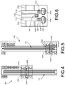
- FIG. 5 is a top view of a combline filter 500 with three transmission lines according to an example implementation.
- the combline filter 500 can be included in an integrated circuit, such as the integrated circuit 100 described above.
- the transmission lines 512 can have similar features and/or functionality as the transmission lines 112 A, 112 B, 114 described above.
- the combline filter 500 can include feedlines 502 A, 502 B with similar features and/or functionalities as the feedlines 302 A, 302 B described above.
- the combline filter 500 can include signal processors 522 A, 522 B coupled to the feedlines 502 A, 502 B.
- the signal processors 522 A, 522 B can process the electromagnetic signals filtered by the combline filter 500 .
- FIG. 6 is a top view of a portion of the combline filter 500 of FIG. 5 according to an example implementation.
- capacitors 502 A, 502 B which can correspond to and/or have similar features and/or functionalities as the capacitors 102 A, 102 B, can be wider than transmission lines 512 A, 512 B, which can have similar features and/or functionalities as the transmission lines 112 A, 112 B.
- each transmission line 512 A, 512 B is coupled to four vias 522 A, 522 B, 522 C, 522 D (vias 522 E and 524 each represent four vias).
- the groups of four vias 522 A, 522 B, 522 C, 522 D, 522 E, 524 can correspond to the vias 110 A, 110 B, 116 A, 116 B described above.
- FIG. 7 is a top view of a combline filter according to an example implementation.
- the frequency responses shown in FIGS. 8A and 8B are based on input to the combline filter of FIG. 7 .
- the combline filter can include transmission lines 712 A, 712 B, 714 corresponding to the transmission lines 112 A, 112 B, 114 described above, capacitors 702 A, 702 B corresponding to the capacitors 102 A, 102 B described above, feedlines 742 A, 742 B corresponding to the feedlines 302 A, 302 B described above, and signal processors 722 A, 722 B corresponding to the signal processors 420 A, 420 B, 522 A, 522 B described above.
- the combline filter can include nodes 736 A, 736 B coupled to ground 738 A, 738 B and to a load 734 A, 734 B, nodes 732 A, 732 B coupled to the signal processors 722 A, 722 B and the load 734 A, 734 B of 50 Ohms, and nodes 730 A, 730 B coupled to the loads 734 A, 734 B.
- the tested signal can have a center frequency of 7 GHz.
- FIG. 8A is a graph showing a frequency response of a combline response according to an example implementation. The loss is minimized, and the passed signals maximized, at and around the center frequency of 7 GHz.
- FIG. 8B is another graph showing a frequency response of a combline filter according to an example implementation.
- FIG. 9 is a top view of a wafer 900 including multiple integrated circuits 100 A, 100 B, 100 C, 100 D according to an example implementation.
- the integrated circuits 100 A, 100 B, 100 C, 100 D can include any combination of the integrated circuit 100 described above. While four integrated circuits 100 A, 100 B, 100 C, 100 D are shown in FIG. 9 , the wafer 900 can include any number of integrated circuits 100 A, 100 B, 100 C, 100 D.
- the wafer 900 can be manufactured according to silicon Very Large Scale Integrated (VLSI) technology.
- VLSI Very Large Scale Integrated
- a singular form may, unless definitely indicating a particular case in terms of the context, include a plural form.
- Spatially relative terms e.g., over, above, upper, under, beneath, below, lower, and so forth
- the relative terms above and below can, respectively, include vertically above and vertically below.
- the term adjacent can include laterally adjacent to or horizontally adjacent to.
- Implementations of the various techniques described herein may be implemented in (e.g., included in) digital electronic circuitry, or in computer hardware, firmware, software, or in combinations of them. Portions of methods also may be performed by, and an apparatus may be implemented as, special purpose logic circuitry, e.g., an FPGA (field programmable gate array) or an ASIC (application specific integrated circuit).
- FPGA field programmable gate array
- ASIC application specific integrated circuit
- Some implementations may be implemented using various semiconductor processing and/or packaging techniques. Some implementations may be implemented using various types of semiconductor processing techniques associated with semiconductor substrates including, but not limited to, for example, Silicon (Si), Gallium Arsenide (GaAs), Gallium Nitride (GaN), Silicon Carbide (SiC) and/or so forth.
- semiconductor substrates including, but not limited to, for example, Silicon (Si), Gallium Arsenide (GaAs), Gallium Nitride (GaN), Silicon Carbide (SiC) and/or so forth.
Landscapes
- Physics & Mathematics (AREA)
- Electromagnetism (AREA)
- Engineering & Computer Science (AREA)
- Microelectronics & Electronic Packaging (AREA)
- Power Engineering (AREA)
- Computer Hardware Design (AREA)
- Condensed Matter Physics & Semiconductors (AREA)
- General Physics & Mathematics (AREA)
- Semiconductor Integrated Circuits (AREA)
- Geometry (AREA)
Abstract
Description
Claims (20)
Priority Applications (3)
| Application Number | Priority Date | Filing Date | Title |
|---|---|---|---|
| US16/107,377 US10862185B2 (en) | 2017-12-01 | 2018-08-21 | Integrated circuit with capacitor in different layer than transmission line |
| CN201821832101.5U CN209515661U (en) | 2017-12-01 | 2018-11-08 | Integrated Circuits and Chips |
| KR1020180152457A KR20190065164A (en) | 2017-12-01 | 2018-11-30 | Integrated circuit with capacitor in different layer than transmission line |
Applications Claiming Priority (2)
| Application Number | Priority Date | Filing Date | Title |
|---|---|---|---|
| US201762593725P | 2017-12-01 | 2017-12-01 | |
| US16/107,377 US10862185B2 (en) | 2017-12-01 | 2018-08-21 | Integrated circuit with capacitor in different layer than transmission line |
Publications (2)
| Publication Number | Publication Date |
|---|---|
| US20190173148A1 US20190173148A1 (en) | 2019-06-06 |
| US10862185B2 true US10862185B2 (en) | 2020-12-08 |
Family
ID=66659555
Family Applications (1)
| Application Number | Title | Priority Date | Filing Date |
|---|---|---|---|
| US16/107,377 Active 2038-10-20 US10862185B2 (en) | 2017-12-01 | 2018-08-21 | Integrated circuit with capacitor in different layer than transmission line |
Country Status (3)
| Country | Link |
|---|---|
| US (1) | US10862185B2 (en) |
| KR (1) | KR20190065164A (en) |
| CN (1) | CN209515661U (en) |
Citations (9)
| Publication number | Priority date | Publication date | Assignee | Title |
|---|---|---|---|---|
| US4638271A (en) * | 1983-05-31 | 1987-01-20 | Thomson-Csf | Method of incrementally adjusting the center frequency of a microstrip-line printed filter by manuevering dielectric layers |
| CA2004184A1 (en) | 1988-11-30 | 1990-05-31 | Henri Budan | Band-pass passive filter |
| US5343176A (en) * | 1992-08-10 | 1994-08-30 | Applied Radiation Laboratories | Radio frequency filter having a substrate with recessed areas |
| US20010030588A1 (en) * | 2000-04-06 | 2001-10-18 | Mi-Hyun Son | Radio filter of combline structure with capacitor compensation circuit |
| US6323745B1 (en) * | 1999-09-09 | 2001-11-27 | Qualcomm Inc. | Planar bandpass filter |
| US20030048156A1 (en) * | 2000-07-24 | 2003-03-13 | Kazuhide Uriu | Laminated band pass filter, high frequency radio equipment, and method of manufacturing laminated band pass filter |
| US20050200436A1 (en) * | 2004-02-14 | 2005-09-15 | Samsung Electronics Co., Ltd. | Compact multilayer band-pass filter and method using interdigital capacitor |
| US8410578B2 (en) | 2006-12-29 | 2013-04-02 | Semiconductor Components Industries, Llc | Method of manufacturing a semiconductor component and structure |
| WO2013141897A1 (en) | 2012-03-21 | 2013-09-26 | Powerwave Technologies, Inc. | Lightweight cavity filter and radio subsystem structures |
-
2018
- 2018-08-21 US US16/107,377 patent/US10862185B2/en active Active
- 2018-11-08 CN CN201821832101.5U patent/CN209515661U/en active Active
- 2018-11-30 KR KR1020180152457A patent/KR20190065164A/en not_active Withdrawn
Patent Citations (11)
| Publication number | Priority date | Publication date | Assignee | Title |
|---|---|---|---|---|
| US4638271A (en) * | 1983-05-31 | 1987-01-20 | Thomson-Csf | Method of incrementally adjusting the center frequency of a microstrip-line printed filter by manuevering dielectric layers |
| CA2004184A1 (en) | 1988-11-30 | 1990-05-31 | Henri Budan | Band-pass passive filter |
| EP0373028A1 (en) | 1988-11-30 | 1990-06-13 | Thomson Hybrides | Passive band-pass filter |
| US5343176A (en) * | 1992-08-10 | 1994-08-30 | Applied Radiation Laboratories | Radio frequency filter having a substrate with recessed areas |
| US6323745B1 (en) * | 1999-09-09 | 2001-11-27 | Qualcomm Inc. | Planar bandpass filter |
| US20010030588A1 (en) * | 2000-04-06 | 2001-10-18 | Mi-Hyun Son | Radio filter of combline structure with capacitor compensation circuit |
| US20030048156A1 (en) * | 2000-07-24 | 2003-03-13 | Kazuhide Uriu | Laminated band pass filter, high frequency radio equipment, and method of manufacturing laminated band pass filter |
| US20050200436A1 (en) * | 2004-02-14 | 2005-09-15 | Samsung Electronics Co., Ltd. | Compact multilayer band-pass filter and method using interdigital capacitor |
| US8410578B2 (en) | 2006-12-29 | 2013-04-02 | Semiconductor Components Industries, Llc | Method of manufacturing a semiconductor component and structure |
| US9564672B2 (en) | 2011-03-22 | 2017-02-07 | Intel Corporation | Lightweight cavity filter structure |
| WO2013141897A1 (en) | 2012-03-21 | 2013-09-26 | Powerwave Technologies, Inc. | Lightweight cavity filter and radio subsystem structures |
Non-Patent Citations (1)
| Title |
|---|
| Xin Wang et al., "CMOS 170 GHz Combline Bandpass Filter," 2015 IEEE MTT-S International Conference on Microwaves for Intelligent Mobility. |
Also Published As
| Publication number | Publication date |
|---|---|
| KR20190065164A (en) | 2019-06-11 |
| CN209515661U (en) | 2019-10-18 |
| US20190173148A1 (en) | 2019-06-06 |
Similar Documents
| Publication | Publication Date | Title |
|---|---|---|
| US8324979B2 (en) | Coupled microstrip lines with ground planes having ground strip shields and ground conductor extensions | |
| US8279025B2 (en) | Slow-wave coaxial transmission line having metal shield strips and dielectric strips with minimum dimensions | |
| RU2158992C2 (en) | Connection structure of elements of high- frequency microchips | |
| JP5337041B2 (en) | Circuit equipment | |
| US20140204806A1 (en) | Duplexer, circuit structure thereof and rf transceiver apparatus comprising the duplexer | |
| US10122341B2 (en) | Coupled-line balun with common-mode nulling | |
| CN106328597A (en) | Electronic apparatus operable in high frequencies | |
| US3678433A (en) | Rf rejection filter | |
| CN1200208A (en) | Coplanar mixer assembly | |
| US9640530B2 (en) | Semiconductor device | |
| US10862185B2 (en) | Integrated circuit with capacitor in different layer than transmission line | |
| CN108376679B (en) | Embedded harmonic terminal of high power RF transistor | |
| JP6320167B2 (en) | Wilkinson distributor and high frequency circuit | |
| CN115050539A (en) | IPD-based 3D inductor with ultrahigh self-resonant frequency and application thereof | |
| US10304612B2 (en) | Common mode filter | |
| US20250309851A1 (en) | Filter module and antenna module including the same | |
| US9520634B2 (en) | Resonance device | |
| US10811755B2 (en) | Microstrip capacitors with complementary resonator structures | |
| US10249581B2 (en) | Transmission line for 3D integrated circuit | |
| CN111279613A (en) | Elliptical structure for bulk acoustic wave resonator | |
| Guan et al. | A low loss and high selectivity GaN-on-Si on-chip bandpass filter | |
| US12249748B2 (en) | Edge capacitive coupling for quantum chips | |
| US20220254717A1 (en) | Semiconductor Device And Manufacturing Method Therefor | |
| US11342647B2 (en) | Free-form dual dual-conductor integrated radio frequency media | |
| US20230317635A1 (en) | Rf chip, structure and method for rf chip guard-ring arrangement |
Legal Events
| Date | Code | Title | Description |
|---|---|---|---|
| AS | Assignment |
Owner name: SEMICONDUCTOR COMPONENTS INDUSTRIES, LLC, ARIZONA Free format text: ASSIGNMENT OF ASSIGNORS INTEREST;ASSIGNOR:EILERT, KIMBERLY DAWN;REEL/FRAME:046651/0650 Effective date: 20180816 |
|
| FEPP | Fee payment procedure |
Free format text: ENTITY STATUS SET TO UNDISCOUNTED (ORIGINAL EVENT CODE: BIG.); ENTITY STATUS OF PATENT OWNER: LARGE ENTITY |
|
| AS | Assignment |
Owner name: DEUTSCHE BANK AG NEW YORK BRANCH, AS COLLATERAL AG Free format text: SECURITY INTEREST;ASSIGNORS:SEMICONDUCTOR COMPONENTS INDUSTRIES, LLC;FAIRCHILD SEMICONDUCTOR CORPORATION;REEL/FRAME:047399/0631 Effective date: 20181018 Owner name: DEUTSCHE BANK AG NEW YORK BRANCH, AS COLLATERAL AGENT, NEW YORK Free format text: SECURITY INTEREST;ASSIGNORS:SEMICONDUCTOR COMPONENTS INDUSTRIES, LLC;FAIRCHILD SEMICONDUCTOR CORPORATION;REEL/FRAME:047399/0631 Effective date: 20181018 |
|
| STPP | Information on status: patent application and granting procedure in general |
Free format text: DOCKETED NEW CASE - READY FOR EXAMINATION |
|
| STPP | Information on status: patent application and granting procedure in general |
Free format text: NON FINAL ACTION MAILED |
|
| STPP | Information on status: patent application and granting procedure in general |
Free format text: RESPONSE TO NON-FINAL OFFICE ACTION ENTERED AND FORWARDED TO EXAMINER |
|
| STPP | Information on status: patent application and granting procedure in general |
Free format text: NON FINAL ACTION MAILED |
|
| STCF | Information on status: patent grant |
Free format text: PATENTED CASE |
|
| CC | Certificate of correction | ||
| AS | Assignment |
Owner name: FAIRCHILD SEMICONDUCTOR CORPORATION, ARIZONA Free format text: RELEASE OF SECURITY INTEREST IN PATENTS RECORDED AT REEL 047399, FRAME 0631;ASSIGNOR:DEUTSCHE BANK AG NEW YORK BRANCH, AS COLLATERAL AGENT;REEL/FRAME:064078/0001 Effective date: 20230622 Owner name: SEMICONDUCTOR COMPONENTS INDUSTRIES, LLC, ARIZONA Free format text: RELEASE OF SECURITY INTEREST IN PATENTS RECORDED AT REEL 047399, FRAME 0631;ASSIGNOR:DEUTSCHE BANK AG NEW YORK BRANCH, AS COLLATERAL AGENT;REEL/FRAME:064078/0001 Effective date: 20230622 |
|
| MAFP | Maintenance fee payment |
Free format text: PAYMENT OF MAINTENANCE FEE, 4TH YEAR, LARGE ENTITY (ORIGINAL EVENT CODE: M1551); ENTITY STATUS OF PATENT OWNER: LARGE ENTITY Year of fee payment: 4 |