US10862182B2 - RF phase shifter comprising a differential transmission line having overlapping sections with tunable dielectric material for phase shifting signals - Google Patents
RF phase shifter comprising a differential transmission line having overlapping sections with tunable dielectric material for phase shifting signals Download PDFInfo
- Publication number
- US10862182B2 US10862182B2 US16/055,225 US201816055225A US10862182B2 US 10862182 B2 US10862182 B2 US 10862182B2 US 201816055225 A US201816055225 A US 201816055225A US 10862182 B2 US10862182 B2 US 10862182B2
- Authority
- US
- United States
- Prior art keywords
- electrode
- transmission line
- phase shifting
- shifting device
- radio frequency
- Prior art date
- Legal status (The legal status is an assumption and is not a legal conclusion. Google has not performed a legal analysis and makes no representation as to the accuracy of the status listed.)
- Active, expires
Links
Images


Classifications
-
- H—ELECTRICITY
- H01—ELECTRIC ELEMENTS
- H01P—WAVEGUIDES; RESONATORS, LINES, OR OTHER DEVICES OF THE WAVEGUIDE TYPE
- H01P1/00—Auxiliary devices
- H01P1/18—Phase-shifters
- H01P1/181—Phase-shifters using ferroelectric devices
-
- H—ELECTRICITY
- H01—ELECTRIC ELEMENTS
- H01P—WAVEGUIDES; RESONATORS, LINES, OR OTHER DEVICES OF THE WAVEGUIDE TYPE
- H01P1/00—Auxiliary devices
- H01P1/18—Phase-shifters
- H01P1/184—Strip line phase-shifters
-
- H—ELECTRICITY
- H01—ELECTRIC ELEMENTS
- H01P—WAVEGUIDES; RESONATORS, LINES, OR OTHER DEVICES OF THE WAVEGUIDE TYPE
- H01P5/00—Coupling devices of the waveguide type
- H01P5/02—Coupling devices of the waveguide type with invariable factor of coupling
- H01P5/022—Transitions between lines of the same kind and shape, but with different dimensions
- H01P5/028—Transitions between lines of the same kind and shape, but with different dimensions between strip lines
-
- H—ELECTRICITY
- H01—ELECTRIC ELEMENTS
- H01Q—ANTENNAS, i.e. RADIO AERIALS
- H01Q21/00—Antenna arrays or systems
- H01Q21/0006—Particular feeding systems
- H01Q21/0075—Stripline fed arrays
-
- H—ELECTRICITY
- H01—ELECTRIC ELEMENTS
- H01Q—ANTENNAS, i.e. RADIO AERIALS
- H01Q3/00—Arrangements for changing or varying the orientation or the shape of the directional pattern of the waves radiated from an antenna or antenna system
- H01Q3/26—Arrangements for changing or varying the orientation or the shape of the directional pattern of the waves radiated from an antenna or antenna system varying the relative phase or relative amplitude of energisation between two or more active radiating elements; varying the distribution of energy across a radiating aperture
- H01Q3/30—Arrangements for changing or varying the orientation or the shape of the directional pattern of the waves radiated from an antenna or antenna system varying the relative phase or relative amplitude of energisation between two or more active radiating elements; varying the distribution of energy across a radiating aperture varying the relative phase between the radiating elements of an array
- H01Q3/34—Arrangements for changing or varying the orientation or the shape of the directional pattern of the waves radiated from an antenna or antenna system varying the relative phase or relative amplitude of energisation between two or more active radiating elements; varying the distribution of energy across a radiating aperture varying the relative phase between the radiating elements of an array by electrical means
- H01Q3/36—Arrangements for changing or varying the orientation or the shape of the directional pattern of the waves radiated from an antenna or antenna system varying the relative phase or relative amplitude of energisation between two or more active radiating elements; varying the distribution of energy across a radiating aperture varying the relative phase between the radiating elements of an array by electrical means with variable phase-shifters
- H01Q3/38—Arrangements for changing or varying the orientation or the shape of the directional pattern of the waves radiated from an antenna or antenna system varying the relative phase or relative amplitude of energisation between two or more active radiating elements; varying the distribution of energy across a radiating aperture varying the relative phase between the radiating elements of an array by electrical means with variable phase-shifters the phase-shifters being digital
-
- H—ELECTRICITY
- H01—ELECTRIC ELEMENTS
- H01Q—ANTENNAS, i.e. RADIO AERIALS
- H01Q3/00—Arrangements for changing or varying the orientation or the shape of the directional pattern of the waves radiated from an antenna or antenna system
- H01Q3/44—Arrangements for changing or varying the orientation or the shape of the directional pattern of the waves radiated from an antenna or antenna system varying the electric or magnetic characteristics of reflecting, refracting, or diffracting devices associated with the radiating element
-
- H—ELECTRICITY
- H01—ELECTRIC ELEMENTS
- H01G—CAPACITORS; CAPACITORS, RECTIFIERS, DETECTORS, SWITCHING DEVICES, LIGHT-SENSITIVE OR TEMPERATURE-SENSITIVE DEVICES OF THE ELECTROLYTIC TYPE
- H01G7/00—Capacitors in which the capacitance is varied by non-mechanical means; Processes of their manufacture
- H01G7/06—Capacitors in which the capacitance is varied by non-mechanical means; Processes of their manufacture having a dielectric selected for the variation of its permittivity with applied voltage, i.e. ferroelectric capacitors
-
- H—ELECTRICITY
- H01—ELECTRIC ELEMENTS
- H01Q—ANTENNAS, i.e. RADIO AERIALS
- H01Q21/00—Antenna arrays or systems
- H01Q21/06—Arrays of individually energised antenna units similarly polarised and spaced apart
- H01Q21/061—Two dimensional planar arrays
- H01Q21/065—Patch antenna array
Definitions
- the invention relates to a radio frequency phase shifting device with a transmission line comprising a first electrode and a second electrode that are spaced at a distance from each other, and which are used for propagation of a radio frequency electromagnetic signal along the first electrode and the second electrode with a phase difference of 180° between the respective electromagnetic signals, wherein a tunable dielectric material affects a phase shift of the electromagnetic signal that is propagated along the transmission line.
- Phase shifting devices can be used to modify the relative displacement between two corresponding features like peaks or zero crossings of an electromagnetic wave or signal without changing the frequency of the electromagnetic wave or signal.
- the electromagnetic signals can be reinforced or weakened.
- the phase difference between the radiated electromagnetic waves will determine a direction of a reinforced superposition of the electromagnetic waves, resulting in a preferred direction of irradiation originating from the respective antennas.
- phase shifting devices with a tunable phase difference are known and described for example in EP 2 761 693 A1 or EP 2 956 986 Bl.
- These phase shifting devices include a linear transmission line comprising a first electrode and a second electrode that are spaced at a distance to each other, wherein a tunable dielectric material is arranged between the first electrode and the second electrode.
- the phase difference created by a tunable phase shifting device can be tuned, i.e. it can be operated to produce different phase differences whereby the respective phase difference can be modified and controlled by a control setting applied to the tunable dielectric material which affects the phase of the signal along the linear transmission line.
- a phased array antenna with several antennas that are interconnected with such tunable phase shifting devices can be operated in such a manner as to change the direction of enhanced signal sensitivity or signal emission in accordance to the requirements at a given time.
- phase shifting device meaning a device which dynamically can adjust the phase or the delay of a radiofrequency signal.
- phase shifting device for each radiating element of the array antenna.
- Each phase shifter device in turn is fed by a feed network. Due to the usually required large number of radiating elements, an at least equally large number of phase shifting devices must be integrated within a limited area in such a phase array antenna.
- the present invention relates to a radio frequency phase shifting device with a transmission line with a first electrode and a second electrode, wherein the transmission line comprises several non-overlapping sections, wherein the first electrode extends at a distance from the second electrode, and wherein the transmission line comprises several overlapping sections, wherein an overlapping area of the first electrode is overlapped by a capacitor electrode area and wherein an overlapping area of the second electrode is overlapped by a capacitor electrode area in order to provide for a parallel plate capacitor area within the overlapping section, and wherein a tunable dielectric material is arranged between the respective capacitor electrode areas and the overlapping area of the first electrode and the overlapping area of the second electrode that affects the phase of a radio frequency electromagnetic signal that propagates along the overlapping section of the transmission line.
- the transmission line with non-overlapping sections and with overlapping sections is similar to a periodically loaded differential or balanced transmission line.
- the resulting phase shift depends inter alia on the number and the area of the parallel plate conductor areas that are implemented along the transmission line.
- the first electrode and the second electrode are arranged side by side, and a capacitor electrode is arranged above or below the first electrode and the second electrode in such a manner that a first capacitor electrode area overlaps the overlapping area of the first electrode and that a second capacitor electrode area overlaps the overlapping area of the second electrode, thus providing for two parallel plate capacitor areas between the capacitor electrode and the respective overlapping areas within the overlapping section.
- the first electrode and the second electrode may be arranged next to another on the same level of the phase shifting device.
- at least one or a few, but preferably many capacitor electrodes are arranged at another level below or above or below and above the first and second electrodes. The use of separate capacitor electrodes allows for complex shapes of the parallel plate capacitor areas along the transmission line and may simplify the manufacturing of the phase shift device.
- each of the overlapping areas of the first electrode and/or of the second electrode is laterally protruding from the respective strip-shaped transmission line segment of the first electrode and/or of the second electrode.
- the combined shape of the first electrode and the second electrode can be similar to a ladder, wherein the strip-shaped transmission line segment of the first electrode and of the second electrode are similar to the first and second ladder beams, and wherein the laterally protruding overlapping areas are similar to the rungs of the ladder.
- Each rung of the ladder comprises one overlapping area that protrudes from the strip-shaped transmission line segment of the first electrode, and one overlapping area that protrudes from the strip-shaped transmission line segment of the second electrode. Even though the two respective overlapping areas of the first and second electrode do overlap, they are spaced apart and separated by the tunable dielectric material that is between the first electrode and the second electrode, or at least between the overlapping areas of the first electrode and the second electrode.
- the respective overlapping areas of the first electrode and the second electrode provide for a rectangular or a square-shaped parallel plate capacitor area.
- the overlapping areas may have any shape and contour that is advantageous for the desired phase shift or for the design of the electronic component that includes the phase shifting device.
- subsequent parallel plate capacitor areas along the transmission line differ in respective distance to each other and/or in size and/or in shape.
- the parallel plate capacitor areas may be of identical shape and size and may be arranged in a regular pattern along the transmission line.
- the distance between two adjacent parallel plate capacitor areas may vary according to demands related to size or cost of the phase shifting device, or in order to allow for better signal propagation or enhanced phase shifting properties of the phase shifting device.
- the first and second electrode can be referenced to one or more ground electrodes located on the outward facing surfaces of the substrate layers.
- the phase shifting device does not rely on the presence of a ground electrode. If, for example for reasons of integrating the sandwich structure with other layers of a phased array antenna, one or more ground electrodes are necessary, the size and the distance of the strip shaped transmission line segments can be easily adjusted when compared to a phase shifting device without ground electrodes.
- the first electrode is connected to a first bias electrode which is connected to the bias voltage source, and that the second electrode is connected to a second bias electrode which is connected to the bias voltage source.
- the width of the bias electrode can be small when compared to the width of the first electrode and of the second electrode.
- the width can be approx. 10% or less of the width of the first or second electrode.
- a small width or cross-section area of the first and second bias electrodes contributes to a high impedance of the first and second bias electrode resulting in reduced leakage of the electromagnetic signal from the first and second electrode into the first or second bias electrode.
- the first and second bias electrodes consists of a material with a lower electrical conductivity that the first and second electrode.
- the resulting higher resistance of the bias electrodes prevents the electromagnetic signal that propagates along the transmission line from leaking from the first and second electrode into the first or second bias electrode.
- the first and second electrode are made of or comprise a material with a high conductivity of more than 40*10 6 S/m, like for example gold or copper.
- the first and second bias electrodes preferably has a sheet resistance of more than 20 Ohms/square and can be made of or comprise Indium Tin Oxide (ITO) or Nichrome (NiCr).
- the invention also relates to a phased array antenna comprising several antenna elements that are arranged at a surface of a substrate layer, a single entry point at which a signal is transmitted to or from the several antenna elements, and for each antenna element a corresponding phase shifting device as described above, wherein the phase of each signal that is transmitted from the single entry point to the respective antenna element or that is transmitted from the respective antenna element to the single entry point is modified in order to adjust the superposition of each signal according to the preferred direction of radiation of the antenna system.
- the phased array antenna comprises, in a stacked arrangement, a base layer with an entry point, a first substrate layer with a first electrode, a tunable layer that comprises the tunable dielectric material, a second substrate layer with a second electrode and an antenna layer with a radiating antenna structure.
- the first and second electrode can be arranged onto the respective surface of the first and second substrate layer by any suitable method, for example by printing or vapor deposition or by any method used within the semiconductor industry.
- the lateral dimension of the phased array antenna can be some millimeters or up to some centimeters or decimeters. The dimensions are preferably adapted to the frequency of the electromagnetic signal that is received or emitted by the respective antennas.
- FIG. 2 illustrates a schematic top view of a transmission line of a single phase shifting device.
- FIG. 3 illustrates a sectional view of the transmission line as shown in FIG. 2 taken along the line III-III.
- FIG. 4 illustrates a sectional view of the transmission line as shown in FIG. 2 taken along the line IV-IV.
- FIG. 5 illustrates a topological representation of the transmission line as shown in FIG. 2 .
- FIG. 6 illustrates a schematic top view of a transmission line of a single phase shifting device, wherein strip-shaped transmission line segments of the first and second electrode are arranged in a zig-zag pattern.
- FIG. 7 a illustrates a first electrode
- FIG. 7 b illustrates a second electrode
- FIG. 7 c is a schematic top view of a transmission line of a single phase shifting device, wherein the strip-shaped transmission line segments exhibit a square-wave meandering pattern combining the first electrode of FIG. 7 a and the second electrode of FIG. 7 b.
- FIG. 8 illustrates a schematic top view of a transmission line of a single phase shifting device, wherein parallel plate capacitor areas along the transmission line differ in size and in shape.
- FIG. 9 illustrates a schematic top view of a transmission line of a single phase shifting device, wherein the first electrode and the second electrode are overlapped by several capacitor electrodes.
- FIG. 10 illustrates a sectional view of the transmission line as shown in FIG. 9 taken along the line X-X.
- FIG. 11 illustrates a sectional view of the transmission line as shown in FIG. 9 taken along the line XI-XI.
- a phased array antenna 1 that is shown in FIG. 1 comprises 64 individual antenna elements 2 that are arranged in a square-shaped grid pattern with 8 ⁇ 8 antenna elements 2 .
- An electromagnetic signal preferably a radiofrequency signal
- An electromagnetic signal can be introduced into the phased array antenna 1 by the signal feed point 3 and distributed to all of the respective antenna elements 2 .
- an electromagnetic signal that is received by the individual antenna elements 2 of the phased array antenna 1 can be transmitted to the signal feed point 3 and extracted from the phased array antenna. All individual antenna elements 2 are connected with the signal feed point 3 .
- the connection comprises a dedicated phase shifting device for each individual antenna element 2 , however, the phase shifting devices are not shown in FIG. 1 .
- the phase shifting devices can be the electrical connection of the individual antenna elements 2 to the signal feed point 3 .
- the corresponding phase shifting device is only a part or section of the electrical connection to the signal feed point 3 .
- FIG. 2 illustrates a schematic top view of a transmission line 4 of a single phase shifting device.
- the transmission line 4 comprises a first electrode 5 and a second electrode 6 , wherein the first electrode 5 is at a different level with respect to the second electrode 6 , thus resulting in a distance between the first electrode 5 and the second electrode 6 .
- the first electrode 5 is on top of the second electrode 6 .
- the first and second electrode 5 , 6 are shown slightly displaced with respect to each other, and the respective parts of the second electrode 6 that are below the corresponding parts of the first electrode 5 are shown with a dashed line.
- Each of the first and second electrode 5 , 6 comprises a strip-shaped transmission line segment 7 , 8 that extends along a straight line in the direction of a signal propagation direction 9 .
- a rectangular overlapping area 10 , 11 laterally protrudes from the respective strip-shaped transmission line segment 7 , 8 of the first electrode 5 and of the second electrode 6 .
- one overlapping area 10 of the first electrode 5 overlaps with one corresponding overlapping area 11 of the second electrode 6 .
- the two overlapping areas 10 , 11 provide for a parallel plate capacitor area 13 of squared shape when viewed from the top.
- the overlapping sections 12 of the transmission line 4 alternate with non-overlapping sections 14 that only comprises the strip-shaped transmission line segments 7 , 8 that are at a distance to each other and that do not overlap like within the overlapping sections 12 of the transmission line 4 .
- the non-overlapping sections 14 do not change much of the phase of the electromagnetic signal that propagates along the first and second electrode 5 , 6 of the transmission line 4 in the direction of the signal propagation direction 9 .
- each of the overlapping sections 12 affects the phase of the propagating electromagnetic signal resulting in a significant phase shift of up to 2 ⁇ or more from a phase shifting device that can be easily integrated into the phased array antenna 1 of FIG. 1 .
- a first bias electrode 15 is connected to the strip-shaped transmission segment 7 of the first electrode 5 and projects in the opposite direction of the overlapping areas 10 of the first electrode 5 .
- a second bias electrode 16 is connected to the strip-shaped transmission segment 8 of the second electrode 6 and projects in the opposite direction of the overlapping areas 11 of the second electrode 6 .
- the first and second bias electrodes 15 , 16 are connected to a bias voltage source not shown in FIG. 2 .
- the bias voltage source provides for a constant, i.e.
- the electric field is perpendicular to the plane of view, i.e. perpendicular to the parallel plate capacitor areas 13 shown in FIG. 2 .
- the impedance of the first and second bias electrode 15 , 16 is significantly higher than the impedance of the strip-shaped transmission segments 7 , 8 of the first and second electrode 5 , 6 which prevents the propagating electromagnetic signal from leaking from the first and second electrode 5 , 6 into the first and second bias electrode 15 , 16 and away from the transmission line 4 .
- the impedance of the bias electrodes can be further increased.
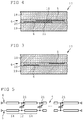
- FIGS. 3 and 4 illustrate two sectional views of a phase shifting device 17 with a transmission line 4 as shown in FIG. 2 .
- FIG. 3 is a sectional view of a non-overlapping section 14 of the transmission line 4 in FIG. 2
- FIG. 4 is a sectional view of an overlapping section 12 of the transmission line 4 in FIG. 2 .
- the first electrode 5 is on top of a first substrate layer 18 made of glass material.
- the second electrode 6 is on top of a second substrate layer 19 also made of glass material.
- the first and second substrate layers 18 , 19 are arranged at a distance to each other with the first electrode 5 facing the second electrode 6 .
- the dielectric properties of the liquid crystal material can be modified by applying different bias voltages to the first and second electrode 5 , 6 resulting in electric fields of different magnitude between the first and second electrode 5 , 6 .
- the overlapping area 10 of the first electrode 5 , the corresponding overlapping area 11 of the second electrode 6 and the liquid crystal material in between provide for a parallel plate capacitor with a capacitance that depends on the bias voltage.
- the topological representation of the transmission line 4 as illustrated in FIG. 5 is that of a periodically loaded differential transmission line with the two electrodes 5 , 6 and capacitive loads 21 of the overlapping sections 12 that alternate with the non-overlapping sections 14 .
- FIG. 6 illustrates a schematic top view of an alternative embodiment of the transmission line 4 , wherein the strip-shaped transmission line segments 7 , 8 of the respective first and second electrode 5 , 6 are arranged in a zig-zag pattern. This allows for longer non-overlapping areas 22 of the respective first and second electrodes 5 , 6 between the overlapping sections 12 along the transmission line 4 as compared to a straight-line arrangement of the transmission line segments 7 , 8 as shown in FIG. 2 .
- FIGS. 7 a , 7 b and 7 c illustrate a schematic top view of a transmission line 4 of a single phase shifting device, wherein the strip-shaped transmission line segments 7 , 8 exhibit a square-wave meandering pattern.
- the first electrode is separately shown in FIG. 7 a
- the second electrode is separately shown in FIG. 7 b
- the overlapping arrangement of both first and second electrode 5 , 6 is shown in FIG. 7 c.
- FIG. 8 illustrates a schematic top view of a transmission line of a single phase shifting device that is similar to the embodiment shown in FIG. 2 .
- the parallel plate capacitor areas 13 along the transmission line 4 differ in size and in shape.
- the distance between subsequent parallel plate capacitor areas 13 may also vary along the transmission line 4 .
- FIG. 9 illustrates a schematic top view of a transmission line of a single phase shifting device, wherein the first electrode 5 and the second electrode 6 each consists of a straight-line strip-shaped transmission line segment 7 , 8 that are directed along the direction of the transmission line 4 that equals the signal propagation direction 9 .
- the transmission line segments 7 , 8 are overlapped by several rectangular capacitor electrodes 23 that are directed perpendicular to the signal propagation direction 9 .
- a first capacitor electrode area 24 of each capacitor electrode 23 overlaps with the corresponding overlapping area 10 of the first electrode 5
- a second capacitor electrode area 25 of each capacitor electrode 23 overlaps with the corresponding overlapping area 11 of the second electrode 6 .
- the first and second capacitor electrode areas 24 , 25 and the corresponding overlapping areas 10 , 11 of the first and second electrode 5 , 6 provide for two separate parallel plate capacitor areas 13 within each overlapping section 12 of the transmission line 4 .
- FIGS. 10 and 11 illustrate two sectional views of a phase shifting device 17 with a transmission line 4 as shown in FIG. 9 .
- FIG. 10 is a sectional view of a non-overlapping section 12 of the transmission line 4 in FIG. 9
- FIG. 11 is a sectional view of an overlapping section 14 of the transmission line 4 in FIG. 9 .
- Both first and second electrode 5 , 6 ( FIG. 11 ) are on the same level and on top of a first substrate layer 18 made of glass material.
- the rectangular capacitor electrodes 23 are on top of a second substrate layer 19 also made of glass material.
- the first and second substrate layers 18 , 19 are arranged at a lateral distance to each other with the first and second electrode 5 , 6 facing the capacitor electrodes 23 .
- first and second substrate layer 18 , 19 there is a tunable layer 20 that is filled with a liquid crystal material.
- the dielectric properties of the liquid crystal material can be modified by applying different bias voltages to the first and second electrode 5 , 6 and to the capacitor electrodes 23 , resulting in electric fields of different magnitude between the first and second electrode 5 , 6 and the respective overlapping areas 24 , 25 ( FIG. 9 ) of the capacitor electrodes 23 .
- the overlapping section 12 as shown in FIG.
- the overlapping area 10 of the first electrode 5 and the corresponding overlapping area 24 of the capacitor electrode 23 as well as the overlapping area 11 of the second electrode 6 and the corresponding overlapping area 25 of the capacitor electrode 23 in combination with the liquid crystal material in between each provide for a parallel plate capacitor area 13 with a capacitance that depends on the bias voltage.
- the bias electrode 16 ( FIG. 10 ) that is connected to all capacitor electrodes 23 is a strip-shaped linear bias electrode 16 that extends parallel to the first and second electrode 5 , 6 , but on the same level as the capacitor electrodes 23 and provides for electrical connection of all the capacitor electrodes 23 with the bias voltage source that is not shown in the figures.
Landscapes
- Waveguide Switches, Polarizers, And Phase Shifters (AREA)
- Variable-Direction Aerials And Aerial Arrays (AREA)
Abstract
Description
Claims (19)
Priority Applications (1)
| Application Number | Priority Date | Filing Date | Title |
|---|---|---|---|
| US16/055,225 US10862182B2 (en) | 2018-08-06 | 2018-08-06 | RF phase shifter comprising a differential transmission line having overlapping sections with tunable dielectric material for phase shifting signals |
Applications Claiming Priority (1)
| Application Number | Priority Date | Filing Date | Title |
|---|---|---|---|
| US16/055,225 US10862182B2 (en) | 2018-08-06 | 2018-08-06 | RF phase shifter comprising a differential transmission line having overlapping sections with tunable dielectric material for phase shifting signals |
Publications (2)
| Publication Number | Publication Date |
|---|---|
| US20200044300A1 US20200044300A1 (en) | 2020-02-06 |
| US10862182B2 true US10862182B2 (en) | 2020-12-08 |
Family
ID=69227626
Family Applications (1)
| Application Number | Title | Priority Date | Filing Date |
|---|---|---|---|
| US16/055,225 Active 2038-08-09 US10862182B2 (en) | 2018-08-06 | 2018-08-06 | RF phase shifter comprising a differential transmission line having overlapping sections with tunable dielectric material for phase shifting signals |
Country Status (1)
| Country | Link |
|---|---|
| US (1) | US10862182B2 (en) |
Cited By (3)
| Publication number | Priority date | Publication date | Assignee | Title |
|---|---|---|---|---|
| US20240106132A1 (en) * | 2021-06-09 | 2024-03-28 | Japan Display Inc. | Intelligent reflecting surface and phased array antenna |
| US12504504B2 (en) | 2022-09-30 | 2025-12-23 | Calterah Semiconductor Technology (Shanghai) Co., Ltd. | Phase shifting system, RF chip, and radar sensor |
| US12573733B2 (en) * | 2022-09-30 | 2026-03-10 | Calterah Semiconductor Technology (Shanghai) Co., Ltd. | Phase shifter, system, chip and radar sensor including plural differential transmission lines that can be adjusted to provide for desired phase shift |
Families Citing this family (10)
| Publication number | Priority date | Publication date | Assignee | Title |
|---|---|---|---|---|
| EP3809517A1 (en) * | 2019-10-17 | 2021-04-21 | ALCAN Systems GmbH | Transmission line for radio frequency signals |
| US12034222B2 (en) | 2020-08-18 | 2024-07-09 | Tmy Technology Inc. | Electromagnetic wave transmission structure |
| TWI788156B (en) * | 2021-09-07 | 2022-12-21 | 稜研科技股份有限公司 | Electromagnetic wave transmission structure |
| US12255409B2 (en) * | 2021-02-09 | 2025-03-18 | Beijing Boe Sensor Technology Co., Ltd. | Array antenna module, manufacturing method thereof, and phased array antenna system |
| EP4145636B1 (en) * | 2021-09-07 | 2024-03-06 | TMY Technology Inc. | Electromagnetic wave transmission structure |
| TWI800998B (en) * | 2021-11-19 | 2023-05-01 | 友達光電股份有限公司 | Phase shifter, antenna cell with the phase shifter and antenna array with the phase shifter |
| CN114361794B (en) * | 2021-12-29 | 2025-06-10 | 广东盛路通信科技股份有限公司 | Phase shifter, integrated feeding network and base station antenna |
| US12334616B2 (en) * | 2022-03-28 | 2025-06-17 | Beijing Boe Technology Development Co., Ltd. | Phase shifter and electronic device |
| US12562506B2 (en) * | 2022-05-20 | 2026-02-24 | Beijing Boe Sensor Technology Co., Ltd. | Antenna, control method thereof, antenna array and electronic device |
| CN120693744A (en) * | 2024-01-23 | 2025-09-23 | 京东方科技集团股份有限公司 | Phase shifter and antenna device |
Citations (31)
| Publication number | Priority date | Publication date | Assignee | Title |
|---|---|---|---|---|
| JPS5893002A (en) | 1981-11-30 | 1983-06-02 | Sumitomo Electric Ind Ltd | Optical waveguide |
| JPS6068701A (en) | 1983-09-22 | 1985-04-19 | Seiko Instr & Electronics Ltd | Crystal oscillation system |
| US5355104A (en) | 1993-01-29 | 1994-10-11 | Hughes Aircraft Company | Phase shift device using voltage-controllable dielectrics |
| JPH077303B2 (en) | 1986-07-07 | 1995-01-30 | フアナツク株式会社 | Robot teaching method |
| US5537242A (en) | 1994-02-10 | 1996-07-16 | Hughes Aircraft Company | Liquid crystal millimeter wave open transmission lines modulators |
| WO1996026554A1 (en) | 1995-02-24 | 1996-08-29 | Thomson-Csf | Microwave phase shifter and use thereof in an array antenna |
| JPH10145103A (en) | 1996-11-08 | 1998-05-29 | Murata Mfg Co Ltd | Four-phase converter and orthogonal modulator using the same |
| EP0887879A1 (en) | 1997-06-23 | 1998-12-30 | Nec Corporation | Phased-array antenna apparatus |
| JP2000315902A (en) | 1999-04-28 | 2000-11-14 | Nippon Hoso Kyokai <Nhk> | Variable phase shifter |
| US20020126048A1 (en) | 1999-09-14 | 2002-09-12 | Yongfei Zhu | Serially-fed phased array antennas with dielectric phase shifters |
| JP2002330006A (en) | 2001-05-02 | 2002-11-15 | Nippon Hoso Kyokai <Nhk> | Variable characteristic high frequency transmission line |
| JP2003008310A (en) | 2001-06-27 | 2003-01-10 | Sumitomo Electric Ind Ltd | High frequency transmission line coupling structure and variable phase shifter using it |
| US6611230B2 (en) * | 2000-12-11 | 2003-08-26 | Harris Corporation | Phased array antenna having phase shifters with laterally spaced phase shift bodies |
| US6759980B2 (en) | 2000-07-21 | 2004-07-06 | Paratek Microwave, Inc. | Phased array antennas incorporating voltage-tunable phase shifters |
| JP2005064632A (en) | 2003-08-08 | 2005-03-10 | Nippon Hoso Kyokai <Nhk> | Variable characteristic high-frequency transmission line |
| US20050110595A1 (en) * | 2003-08-08 | 2005-05-26 | Du Toit Cornelis F. | Loaded line phase shifter |
| US20050128029A1 (en) * | 2003-12-10 | 2005-06-16 | Lee Su J. | Ferroelectric epitaxial thin film for microwave tunable device and microwave tunable device using the same |
| CN1728448A (en) | 2005-07-29 | 2006-02-01 | 华东师范大学 | Aperiodic capacity loaded phase shifter |
| US7145412B2 (en) * | 2000-08-25 | 2006-12-05 | N Gimat Co. | Electronic and optical devices and methods of forming these devices |
| JP2007110256A (en) | 2005-10-11 | 2007-04-26 | Matsushita Electric Ind Co Ltd | Phased array antenna |
| US7361288B2 (en) | 2003-07-11 | 2008-04-22 | Merck Patent Gesellschaft Mit Besschrankter Haftung | Components for high-frequency technology |
| US20080116995A1 (en) * | 2004-12-20 | 2008-05-22 | Electronics And Telecommunications Research Institute | Phase Shifter with Photonic Band Gap Structure Using Ferroelectric Thin Film |
| US7466269B2 (en) | 2006-05-24 | 2008-12-16 | Wavebender, Inc. | Variable dielectric constant-based antenna and array |
| CN101454941A (en) | 2006-05-24 | 2009-06-10 | 韦夫班德尔公司 | Variable dielectric constant based antennas and arrays |
| US20090278744A1 (en) | 2005-10-11 | 2009-11-12 | Panasonic Corporation | Phased array antenna |
| WO2011009524A1 (en) | 2009-07-21 | 2011-01-27 | Merck Patent Gmbh | Liquid crystal medium and high-frequency components containing the same |
| WO2011035863A1 (en) | 2009-09-25 | 2011-03-31 | Merck Patent Gmbh | Components for high-frequency technology and liquid crystal media |
| WO2011036243A1 (en) | 2009-09-25 | 2011-03-31 | Technische Universität Darmstadt | Phase shifter for high-frequency signals |
| EP2768072A1 (en) | 2013-02-15 | 2014-08-20 | Technische Universität Darmstadt | Phase shifting device |
| EP2761693B1 (en) | 2011-09-27 | 2017-05-17 | Technische Universität Darmstadt | Electronically steerable planar phased array antenna |
| US20180287254A1 (en) | 2015-10-09 | 2018-10-04 | Sharp Kabushiki Kaisha | Scanning antenna and method for driving same |
-
2018
- 2018-08-06 US US16/055,225 patent/US10862182B2/en active Active
Patent Citations (45)
| Publication number | Priority date | Publication date | Assignee | Title |
|---|---|---|---|---|
| JPS5893002A (en) | 1981-11-30 | 1983-06-02 | Sumitomo Electric Ind Ltd | Optical waveguide |
| JPS6068701A (en) | 1983-09-22 | 1985-04-19 | Seiko Instr & Electronics Ltd | Crystal oscillation system |
| JPH077303B2 (en) | 1986-07-07 | 1995-01-30 | フアナツク株式会社 | Robot teaching method |
| US5355104A (en) | 1993-01-29 | 1994-10-11 | Hughes Aircraft Company | Phase shift device using voltage-controllable dielectrics |
| US5537242A (en) | 1994-02-10 | 1996-07-16 | Hughes Aircraft Company | Liquid crystal millimeter wave open transmission lines modulators |
| WO1996026554A1 (en) | 1995-02-24 | 1996-08-29 | Thomson-Csf | Microwave phase shifter and use thereof in an array antenna |
| US5936484A (en) | 1995-02-24 | 1999-08-10 | Thomson-Csf | UHF phase shifter and application to an array antenna |
| JPH10145103A (en) | 1996-11-08 | 1998-05-29 | Murata Mfg Co Ltd | Four-phase converter and orthogonal modulator using the same |
| EP0887879A1 (en) | 1997-06-23 | 1998-12-30 | Nec Corporation | Phased-array antenna apparatus |
| JP2000315902A (en) | 1999-04-28 | 2000-11-14 | Nippon Hoso Kyokai <Nhk> | Variable phase shifter |
| US20020126048A1 (en) | 1999-09-14 | 2002-09-12 | Yongfei Zhu | Serially-fed phased array antennas with dielectric phase shifters |
| CN1373916A (en) | 1999-09-14 | 2002-10-09 | 帕拉泰克微波公司 | Serial-Fed Phased Array Antenna with Dielectric Phase Shifter |
| US6864840B2 (en) | 1999-09-14 | 2005-03-08 | Paratek Microwave, Inc. | Serially-fed phased array antennas with dielectric phase shifters |
| US6759980B2 (en) | 2000-07-21 | 2004-07-06 | Paratek Microwave, Inc. | Phased array antennas incorporating voltage-tunable phase shifters |
| US7145412B2 (en) * | 2000-08-25 | 2006-12-05 | N Gimat Co. | Electronic and optical devices and methods of forming these devices |
| US6611230B2 (en) * | 2000-12-11 | 2003-08-26 | Harris Corporation | Phased array antenna having phase shifters with laterally spaced phase shift bodies |
| JP2002330006A (en) | 2001-05-02 | 2002-11-15 | Nippon Hoso Kyokai <Nhk> | Variable characteristic high frequency transmission line |
| JP2003008310A (en) | 2001-06-27 | 2003-01-10 | Sumitomo Electric Ind Ltd | High frequency transmission line coupling structure and variable phase shifter using it |
| US7361288B2 (en) | 2003-07-11 | 2008-04-22 | Merck Patent Gesellschaft Mit Besschrankter Haftung | Components for high-frequency technology |
| JP2005064632A (en) | 2003-08-08 | 2005-03-10 | Nippon Hoso Kyokai <Nhk> | Variable characteristic high-frequency transmission line |
| US20050110595A1 (en) * | 2003-08-08 | 2005-05-26 | Du Toit Cornelis F. | Loaded line phase shifter |
| US20050128029A1 (en) * | 2003-12-10 | 2005-06-16 | Lee Su J. | Ferroelectric epitaxial thin film for microwave tunable device and microwave tunable device using the same |
| US20080116995A1 (en) * | 2004-12-20 | 2008-05-22 | Electronics And Telecommunications Research Institute | Phase Shifter with Photonic Band Gap Structure Using Ferroelectric Thin Film |
| CN1728448A (en) | 2005-07-29 | 2006-02-01 | 华东师范大学 | Aperiodic capacity loaded phase shifter |
| JP2007110256A (en) | 2005-10-11 | 2007-04-26 | Matsushita Electric Ind Co Ltd | Phased array antenna |
| CN101283480A (en) | 2005-10-11 | 2008-10-08 | 松下电器产业株式会社 | phased array antenna |
| US20090278744A1 (en) | 2005-10-11 | 2009-11-12 | Panasonic Corporation | Phased array antenna |
| US7466269B2 (en) | 2006-05-24 | 2008-12-16 | Wavebender, Inc. | Variable dielectric constant-based antenna and array |
| US20090091500A1 (en) | 2006-05-24 | 2009-04-09 | Wavebender, Inc. | Variable Dielectric Constant-Based Antenna And Array |
| CN101454941A (en) | 2006-05-24 | 2009-06-10 | 韦夫班德尔公司 | Variable dielectric constant based antennas and arrays |
| JP2009538565A (en) | 2006-05-24 | 2009-11-05 | ウェーブベンダー インコーポレーテッド | Variable dielectric constant based antenna and array |
| EP2020051B1 (en) | 2006-05-24 | 2016-09-28 | Wafer Llc | Variable dielectric constant-based antenna and array |
| US7884766B2 (en) | 2006-05-24 | 2011-02-08 | Wavebender, Inc. | Variable dielectric constant-based antenna and array |
| CN101454941B (en) | 2006-05-24 | 2013-11-20 | D·D·哈兹扎 | Antennas and Arrays Based on Variable Permittivity |
| US20120119141A1 (en) | 2009-07-21 | 2012-05-17 | Merck Patent Gmbh | Liquid crystal medium and high-frequency components containing the same |
| WO2011009524A1 (en) | 2009-07-21 | 2011-01-27 | Merck Patent Gmbh | Liquid crystal medium and high-frequency components containing the same |
| WO2011036243A1 (en) | 2009-09-25 | 2011-03-31 | Technische Universität Darmstadt | Phase shifter for high-frequency signals |
| US20120182200A1 (en) | 2009-09-25 | 2012-07-19 | Merck Patent Gesellschaft Mit Beschrankter Haftung | Components for high-frequency technology, and liquid-crystalline media |
| WO2011035863A1 (en) | 2009-09-25 | 2011-03-31 | Merck Patent Gmbh | Components for high-frequency technology and liquid crystal media |
| EP2761693B1 (en) | 2011-09-27 | 2017-05-17 | Technische Universität Darmstadt | Electronically steerable planar phased array antenna |
| US20190260139A1 (en) | 2011-09-27 | 2019-08-22 | Alcan Systems Gmbh | Electronically steerable planar phase array antenna |
| EP2768072A1 (en) | 2013-02-15 | 2014-08-20 | Technische Universität Darmstadt | Phase shifting device |
| EP2956986B1 (en) | 2013-02-15 | 2017-02-01 | Technische Universität Darmstadt | Phase shift device |
| US20190103644A1 (en) | 2013-02-15 | 2019-04-04 | Alcan Systems Gmbh | Phase shift device |
| US20180287254A1 (en) | 2015-10-09 | 2018-10-04 | Sharp Kabushiki Kaisha | Scanning antenna and method for driving same |
Non-Patent Citations (5)
| Title |
|---|
| Dielectric resonator antenna phased array with liquid crystal based phase shifters, Authors: Mehmood Arshad, Karabey Onur Hamza, Ayluctarhan Muhammed, Zheng Yuliang, Braun Hubertus, Hovhannisyan Martun, Letz Martin, Jakoby Rolf, Publication data: The 8th European Conference on Antennas and Propagation (EuCAP 2014),,Apr. 6, 2014,European Association on Antennas and Propagation, Source info: pp. 2436-2439. |
| Fully printed tunable phase shifter for L/S-band phased array application, Authors: Nikfalazar Mohammad, Kohler Christian, Friederich Andreas, Sazegar Mohsen, Zheng Yuliang, Wiens Alex, Binder Joachim R, Jakoby Rolf, Publication data: 2014 IEEE MTT-S International Microwave Symposium (IMS2014),,Jun. 1, 2014,IEEE, Source info: pp. 1-4. |
| Liquid crystal varactor loaded variable phase shifter for integrated, compact, and fast beamsteering antenna systems, Authors: Hu Wenjuan, Karabey Onur Hamza, Gabler Alexander, Prasetiadi Ananto Eka, Jost Matthias, Jakoby Rolf, Publication data: 2014 9th European Microwave Integrated Circuit Conference,,Oct. 6, 2014,European Microwave Association—EUMA, Source info: pp. 660-663. |
| Reconfigurable and Tunable Metamaterials: A Review of the Theory and Applications, Authors: Jeremiah P Turpin, Jeremy A Bossard, Kenneth L Morgan, Douglas H Werner, Pingjuan L Werner, Publication data: International Journal of Antennas and Propagation,,Jan. 1, 2014, Source info: vol. 11, Nr: 4, pp. 836-818. |
| Tunable loaded line phase shifters for microwave applications, Authors: Onur Hamza Karabey, Felix Goelden, Alexander Gaebler, Sebastian Strunck, Rolf Jakoby, Publication data: Microwave Symposium Digest (MTT), 2011 IEEE MTT-S International,,Jun. 5, 2011,IEEE, Source info: pp. 1-4. |
Cited By (4)
| Publication number | Priority date | Publication date | Assignee | Title |
|---|---|---|---|---|
| US20240106132A1 (en) * | 2021-06-09 | 2024-03-28 | Japan Display Inc. | Intelligent reflecting surface and phased array antenna |
| US12451614B2 (en) * | 2021-06-09 | 2025-10-21 | Japan Display Inc. | Intelligent reflecting surface and phased array antenna |
| US12504504B2 (en) | 2022-09-30 | 2025-12-23 | Calterah Semiconductor Technology (Shanghai) Co., Ltd. | Phase shifting system, RF chip, and radar sensor |
| US12573733B2 (en) * | 2022-09-30 | 2026-03-10 | Calterah Semiconductor Technology (Shanghai) Co., Ltd. | Phase shifter, system, chip and radar sensor including plural differential transmission lines that can be adjusted to provide for desired phase shift |
Also Published As
| Publication number | Publication date |
|---|---|
| US20200044300A1 (en) | 2020-02-06 |
Similar Documents
| Publication | Publication Date | Title |
|---|---|---|
| US10862182B2 (en) | RF phase shifter comprising a differential transmission line having overlapping sections with tunable dielectric material for phase shifting signals | |
| EP3609018B1 (en) | Radio frequency phase shifting device and method of operation for this phase shifting device | |
| CN109193081B (en) | RF Phase Shifter | |
| US10720712B2 (en) | Liquid-crystal tunable metasurface for beam steering antennas | |
| EP3664215B1 (en) | Radio frequency phase shifting device | |
| US10741921B2 (en) | Multi-layered software defined antenna and method of manufacture | |
| US9871293B2 (en) | Two-dimensionally electronically-steerable artificial impedance surface antenna | |
| US9455495B2 (en) | Two-dimensionally electronically-steerable artificial impedance surface antenna | |
| CN113728512B (en) | Phase shifters and antennas | |
| KR20200087861A (en) | Phase-array antennas, display panels, and display devices | |
| US9837695B2 (en) | Surface-wave waveguide with conductive sidewalls and application in antennas | |
| CN105379011A (en) | Electronically steerable, artificial impedance, surface antenna | |
| EP3811467B1 (en) | Electronically beam-steerable, low-sidelobe composite right-left-handed (crlh) metamaterial array antenna | |
| US11158953B2 (en) | Flat-plate, low sidelobe, two-dimensional, steerable leaky-wave planar array antenna | |
| EP3745526A1 (en) | Radio frequency phase shift device | |
| US20250392042A1 (en) | Beamformer | |
| EP3079204A1 (en) | Two-dimensionally electronically-steerable artificial impedance surface antenna | |
| Roig et al. | Tunable frequency selective surface based on ferroelectric ceramics for beam steering antennas | |
| CN118947024A (en) | Reflective element for electric wave using liquid crystal material | |
| AU2014202093B2 (en) | Two-dimensionally electronically-steerable artificial impedance surface antenna |
Legal Events
| Date | Code | Title | Description |
|---|---|---|---|
| FEPP | Fee payment procedure |
Free format text: ENTITY STATUS SET TO UNDISCOUNTED (ORIGINAL EVENT CODE: BIG.); ENTITY STATUS OF PATENT OWNER: SMALL ENTITY |
|
| FEPP | Fee payment procedure |
Free format text: ENTITY STATUS SET TO SMALL (ORIGINAL EVENT CODE: SMAL); ENTITY STATUS OF PATENT OWNER: SMALL ENTITY |
|
| AS | Assignment |
Owner name: ALCAN SYSTEMS GMBH, GERMANY Free format text: ASSIGNMENT OF ASSIGNORS INTEREST;ASSIGNORS:GOELDEN, FELIX;GAEBLER, ALEXANDER;KARABEY, ONUR HAMZA;REEL/FRAME:046751/0234 Effective date: 20180806 |
|
| STPP | Information on status: patent application and granting procedure in general |
Free format text: NON FINAL ACTION MAILED |
|
| STCF | Information on status: patent grant |
Free format text: PATENTED CASE |
|
| AS | Assignment |
Owner name: BEIJING BOE SENSOR TECHNOLOGY CO., LTD., CHINA Free format text: ASSIGNMENT OF ASSIGNORS INTEREST;ASSIGNOR:ALCAN SYSTEMS GMBH;REEL/FRAME:066416/0630 Effective date: 20231221 |
|
| FEPP | Fee payment procedure |
Free format text: ENTITY STATUS SET TO UNDISCOUNTED (ORIGINAL EVENT CODE: BIG.); ENTITY STATUS OF PATENT OWNER: LARGE ENTITY |
|
| MAFP | Maintenance fee payment |
Free format text: PAYMENT OF MAINTENANCE FEE, 4TH YEAR, LARGE ENTITY (ORIGINAL EVENT CODE: M1551); ENTITY STATUS OF PATENT OWNER: LARGE ENTITY Year of fee payment: 4 |
|
| AS | Assignment |
Owner name: BEIJING BOE SENSOR TECHNOLOGY CO., LTD., CHINA Free format text: ASSIGNMENT OF ASSIGNORS INTEREST;ASSIGNOR:ALCAN SYSTEMS GMBH;REEL/FRAME:069237/0325 Effective date: 20231221 |