US10861933B2 - Elongated semiconductor structure planarization - Google Patents
Elongated semiconductor structure planarization Download PDFInfo
- Publication number
- US10861933B2 US10861933B2 US16/179,645 US201816179645A US10861933B2 US 10861933 B2 US10861933 B2 US 10861933B2 US 201816179645 A US201816179645 A US 201816179645A US 10861933 B2 US10861933 B2 US 10861933B2
- Authority
- US
- United States
- Prior art keywords
- semiconductor structures
- elongated semiconductor
- elongated
- portions
- substrate
- Prior art date
- Legal status (The legal status is an assumption and is not a legal conclusion. Google has not performed a legal analysis and makes no representation as to the accuracy of the status listed.)
- Active, expires
Links
Images


Classifications
-
- H01L29/0676—
-
- H—ELECTRICITY
- H10—SEMICONDUCTOR DEVICES; ELECTRIC SOLID-STATE DEVICES NOT OTHERWISE PROVIDED FOR
- H10D—INORGANIC ELECTRIC SEMICONDUCTOR DEVICES
- H10D62/00—Semiconductor bodies, or regions thereof, of devices having potential barriers
- H10D62/10—Shapes, relative sizes or dispositions of the regions of the semiconductor bodies; Shapes of the semiconductor bodies
- H10D62/117—Shapes of semiconductor bodies
- H10D62/118—Nanostructure semiconductor bodies
- H10D62/119—Nanowire, nanosheet or nanotube semiconductor bodies
- H10D62/122—Nanowire, nanosheet or nanotube semiconductor bodies oriented at angles to substrates, e.g. perpendicular to substrates
-
- H—ELECTRICITY
- H10—SEMICONDUCTOR DEVICES; ELECTRIC SOLID-STATE DEVICES NOT OTHERWISE PROVIDED FOR
- H10D—INORGANIC ELECTRIC SEMICONDUCTOR DEVICES
- H10D84/00—Integrated devices formed in or on semiconductor substrates that comprise only semiconducting layers, e.g. on Si wafers or on GaAs-on-Si wafers
- H10D84/01—Manufacture or treatment
- H10D84/0123—Integrating together multiple components covered by H10D12/00 or H10D30/00, e.g. integrating multiple IGBTs
- H10D84/0126—Integrating together multiple components covered by H10D12/00 or H10D30/00, e.g. integrating multiple IGBTs the components including insulated gates, e.g. IGFETs
-
- B—PERFORMING OPERATIONS; TRANSPORTING
- B82—NANOTECHNOLOGY
- B82Y—SPECIFIC USES OR APPLICATIONS OF NANOSTRUCTURES; MEASUREMENT OR ANALYSIS OF NANOSTRUCTURES; MANUFACTURE OR TREATMENT OF NANOSTRUCTURES
- B82Y10/00—Nanotechnology for information processing, storage or transmission, e.g. quantum computing or single electron logic
-
- H—ELECTRICITY
- H01—ELECTRIC ELEMENTS
- H01L—SEMICONDUCTOR DEVICES NOT COVERED BY CLASS H10
- H01L21/00—Processes or apparatus adapted for the manufacture or treatment of semiconductor or solid state devices or of parts thereof
- H01L21/02—Manufacture or treatment of semiconductor devices or of parts thereof
- H01L21/02104—Forming layers
- H01L21/02365—Forming inorganic semiconducting materials on a substrate
- H01L21/02518—Deposited layers
- H01L21/02521—Materials
- H01L21/02524—Group 14 semiconducting materials
- H01L21/02532—Silicon, silicon germanium, germanium
-
- H—ELECTRICITY
- H01—ELECTRIC ELEMENTS
- H01L—SEMICONDUCTOR DEVICES NOT COVERED BY CLASS H10
- H01L21/00—Processes or apparatus adapted for the manufacture or treatment of semiconductor or solid state devices or of parts thereof
- H01L21/02—Manufacture or treatment of semiconductor devices or of parts thereof
- H01L21/02104—Forming layers
- H01L21/02365—Forming inorganic semiconducting materials on a substrate
- H01L21/02518—Deposited layers
- H01L21/02521—Materials
- H01L21/02538—Group 13/15 materials
- H01L21/02546—Arsenides
-
- H—ELECTRICITY
- H01—ELECTRIC ELEMENTS
- H01L—SEMICONDUCTOR DEVICES NOT COVERED BY CLASS H10
- H01L21/00—Processes or apparatus adapted for the manufacture or treatment of semiconductor or solid state devices or of parts thereof
- H01L21/02—Manufacture or treatment of semiconductor devices or of parts thereof
- H01L21/02104—Forming layers
- H01L21/02365—Forming inorganic semiconducting materials on a substrate
- H01L21/02518—Deposited layers
- H01L21/02521—Materials
- H01L21/02538—Group 13/15 materials
- H01L21/02549—Antimonides
-
- H—ELECTRICITY
- H01—ELECTRIC ELEMENTS
- H01L—SEMICONDUCTOR DEVICES NOT COVERED BY CLASS H10
- H01L21/00—Processes or apparatus adapted for the manufacture or treatment of semiconductor or solid state devices or of parts thereof
- H01L21/02—Manufacture or treatment of semiconductor devices or of parts thereof
- H01L21/02104—Forming layers
- H01L21/02365—Forming inorganic semiconducting materials on a substrate
- H01L21/02518—Deposited layers
- H01L21/02587—Structure
- H01L21/0259—Microstructure
- H01L21/02603—Nanowires
-
- H—ELECTRICITY
- H01—ELECTRIC ELEMENTS
- H01L—SEMICONDUCTOR DEVICES NOT COVERED BY CLASS H10
- H01L21/00—Processes or apparatus adapted for the manufacture or treatment of semiconductor or solid state devices or of parts thereof
- H01L21/02—Manufacture or treatment of semiconductor devices or of parts thereof
- H01L21/02104—Forming layers
- H01L21/02365—Forming inorganic semiconducting materials on a substrate
- H01L21/02612—Formation types
- H01L21/02617—Deposition types
- H01L21/02636—Selective deposition, e.g. simultaneous growth of mono- and non-monocrystalline semiconductor materials
- H01L21/02639—Preparation of substrate for selective deposition
- H01L21/02642—Mask materials other than SiO2 or SiN
-
- H—ELECTRICITY
- H01—ELECTRIC ELEMENTS
- H01L—SEMICONDUCTOR DEVICES NOT COVERED BY CLASS H10
- H01L21/00—Processes or apparatus adapted for the manufacture or treatment of semiconductor or solid state devices or of parts thereof
- H01L21/02—Manufacture or treatment of semiconductor devices or of parts thereof
- H01L21/04—Manufacture or treatment of semiconductor devices or of parts thereof the devices having potential barriers, e.g. a PN junction, depletion layer or carrier concentration layer
- H01L21/18—Manufacture or treatment of semiconductor devices or of parts thereof the devices having potential barriers, e.g. a PN junction, depletion layer or carrier concentration layer the devices having semiconductor bodies comprising elements of Group IV of the Periodic Table or AIIIBV compounds with or without impurities, e.g. doping materials
- H01L21/30—Treatment of semiconductor bodies using processes or apparatus not provided for in groups H01L21/20 - H01L21/26
- H01L21/302—Treatment of semiconductor bodies using processes or apparatus not provided for in groups H01L21/20 - H01L21/26 to change their surface-physical characteristics or shape, e.g. etching, polishing, cutting
- H01L21/306—Chemical or electrical treatment, e.g. electrolytic etching
- H01L21/30625—With simultaneous mechanical treatment, e.g. mechanico-chemical polishing
-
- H—ELECTRICITY
- H01—ELECTRIC ELEMENTS
- H01L—SEMICONDUCTOR DEVICES NOT COVERED BY CLASS H10
- H01L21/00—Processes or apparatus adapted for the manufacture or treatment of semiconductor or solid state devices or of parts thereof
- H01L21/02—Manufacture or treatment of semiconductor devices or of parts thereof
- H01L21/04—Manufacture or treatment of semiconductor devices or of parts thereof the devices having potential barriers, e.g. a PN junction, depletion layer or carrier concentration layer
- H01L21/18—Manufacture or treatment of semiconductor devices or of parts thereof the devices having potential barriers, e.g. a PN junction, depletion layer or carrier concentration layer the devices having semiconductor bodies comprising elements of Group IV of the Periodic Table or AIIIBV compounds with or without impurities, e.g. doping materials
- H01L21/30—Treatment of semiconductor bodies using processes or apparatus not provided for in groups H01L21/20 - H01L21/26
- H01L21/31—Treatment of semiconductor bodies using processes or apparatus not provided for in groups H01L21/20 - H01L21/26 to form insulating layers thereon, e.g. for masking or by using photolithographic techniques; After treatment of these layers; Selection of materials for these layers
- H01L21/3205—Deposition of non-insulating-, e.g. conductive- or resistive-, layers on insulating layers; After-treatment of these layers
- H01L21/321—After treatment
- H01L21/32115—Planarisation
- H01L21/3212—Planarisation by chemical mechanical polishing [CMP]
-
- H01L21/823412—
-
- H01L21/823418—
-
- H01L21/823487—
-
- H01L27/088—
-
- H01L29/0688—
-
- H01L29/401—
-
- H01L29/42392—
-
- H01L29/66439—
-
- H01L29/66469—
-
- H01L29/66545—
-
- H01L29/775—
-
- H01L29/7827—
-
- H—ELECTRICITY
- H10—SEMICONDUCTOR DEVICES; ELECTRIC SOLID-STATE DEVICES NOT OTHERWISE PROVIDED FOR
- H10D—INORGANIC ELECTRIC SEMICONDUCTOR DEVICES
- H10D30/00—Field-effect transistors [FET]
- H10D30/01—Manufacture or treatment
- H10D30/014—Manufacture or treatment of FETs having zero-dimensional [0D] or one-dimensional [1D] channels, e.g. quantum wire FETs, single-electron transistors [SET] or Coulomb blockade transistors
-
- H—ELECTRICITY
- H10—SEMICONDUCTOR DEVICES; ELECTRIC SOLID-STATE DEVICES NOT OTHERWISE PROVIDED FOR
- H10D—INORGANIC ELECTRIC SEMICONDUCTOR DEVICES
- H10D30/00—Field-effect transistors [FET]
- H10D30/40—FETs having zero-dimensional [0D], one-dimensional [1D] or two-dimensional [2D] charge carrier gas channels
- H10D30/43—FETs having zero-dimensional [0D], one-dimensional [1D] or two-dimensional [2D] charge carrier gas channels having 1D charge carrier gas channels, e.g. quantum wire FETs or transistors having 1D quantum-confined channels
-
- H—ELECTRICITY
- H10—SEMICONDUCTOR DEVICES; ELECTRIC SOLID-STATE DEVICES NOT OTHERWISE PROVIDED FOR
- H10D—INORGANIC ELECTRIC SEMICONDUCTOR DEVICES
- H10D30/00—Field-effect transistors [FET]
- H10D30/60—Insulated-gate field-effect transistors [IGFET]
- H10D30/63—Vertical IGFETs
-
- H—ELECTRICITY
- H10—SEMICONDUCTOR DEVICES; ELECTRIC SOLID-STATE DEVICES NOT OTHERWISE PROVIDED FOR
- H10D—INORGANIC ELECTRIC SEMICONDUCTOR DEVICES
- H10D30/00—Field-effect transistors [FET]
- H10D30/60—Insulated-gate field-effect transistors [IGFET]
- H10D30/67—Thin-film transistors [TFT]
- H10D30/6729—Thin-film transistors [TFT] characterised by the electrodes
- H10D30/673—Thin-film transistors [TFT] characterised by the electrodes characterised by the shapes, relative sizes or dispositions of the gate electrodes
- H10D30/6735—Thin-film transistors [TFT] characterised by the electrodes characterised by the shapes, relative sizes or dispositions of the gate electrodes having gates fully surrounding the channels, e.g. gate-all-around
-
- H—ELECTRICITY
- H10—SEMICONDUCTOR DEVICES; ELECTRIC SOLID-STATE DEVICES NOT OTHERWISE PROVIDED FOR
- H10D—INORGANIC ELECTRIC SEMICONDUCTOR DEVICES
- H10D62/00—Semiconductor bodies, or regions thereof, of devices having potential barriers
- H10D62/10—Shapes, relative sizes or dispositions of the regions of the semiconductor bodies; Shapes of the semiconductor bodies
- H10D62/124—Shapes, relative sizes or dispositions of the regions of semiconductor bodies or of junctions between the regions
- H10D62/125—Shapes of junctions between the regions
-
- H—ELECTRICITY
- H10—SEMICONDUCTOR DEVICES; ELECTRIC SOLID-STATE DEVICES NOT OTHERWISE PROVIDED FOR
- H10D—INORGANIC ELECTRIC SEMICONDUCTOR DEVICES
- H10D64/00—Electrodes of devices having potential barriers
- H10D64/01—Manufacture or treatment
-
- H—ELECTRICITY
- H10—SEMICONDUCTOR DEVICES; ELECTRIC SOLID-STATE DEVICES NOT OTHERWISE PROVIDED FOR
- H10D—INORGANIC ELECTRIC SEMICONDUCTOR DEVICES
- H10D64/00—Electrodes of devices having potential barriers
- H10D64/01—Manufacture or treatment
- H10D64/017—Manufacture or treatment using dummy gates in processes wherein at least parts of the final gates are self-aligned to the dummy gates, i.e. replacement gate processes
-
- H—ELECTRICITY
- H10—SEMICONDUCTOR DEVICES; ELECTRIC SOLID-STATE DEVICES NOT OTHERWISE PROVIDED FOR
- H10D—INORGANIC ELECTRIC SEMICONDUCTOR DEVICES
- H10D84/00—Integrated devices formed in or on semiconductor substrates that comprise only semiconducting layers, e.g. on Si wafers or on GaAs-on-Si wafers
- H10D84/01—Manufacture or treatment
- H10D84/0123—Integrating together multiple components covered by H10D12/00 or H10D30/00, e.g. integrating multiple IGBTs
- H10D84/0126—Integrating together multiple components covered by H10D12/00 or H10D30/00, e.g. integrating multiple IGBTs the components including insulated gates, e.g. IGFETs
- H10D84/0128—Manufacturing their channels
-
- H—ELECTRICITY
- H10—SEMICONDUCTOR DEVICES; ELECTRIC SOLID-STATE DEVICES NOT OTHERWISE PROVIDED FOR
- H10D—INORGANIC ELECTRIC SEMICONDUCTOR DEVICES
- H10D84/00—Integrated devices formed in or on semiconductor substrates that comprise only semiconducting layers, e.g. on Si wafers or on GaAs-on-Si wafers
- H10D84/01—Manufacture or treatment
- H10D84/0123—Integrating together multiple components covered by H10D12/00 or H10D30/00, e.g. integrating multiple IGBTs
- H10D84/0126—Integrating together multiple components covered by H10D12/00 or H10D30/00, e.g. integrating multiple IGBTs the components including insulated gates, e.g. IGFETs
- H10D84/013—Manufacturing their source or drain regions, e.g. silicided source or drain regions
-
- H—ELECTRICITY
- H10—SEMICONDUCTOR DEVICES; ELECTRIC SOLID-STATE DEVICES NOT OTHERWISE PROVIDED FOR
- H10D—INORGANIC ELECTRIC SEMICONDUCTOR DEVICES
- H10D84/00—Integrated devices formed in or on semiconductor substrates that comprise only semiconducting layers, e.g. on Si wafers or on GaAs-on-Si wafers
- H10D84/01—Manufacture or treatment
- H10D84/0123—Integrating together multiple components covered by H10D12/00 or H10D30/00, e.g. integrating multiple IGBTs
- H10D84/0126—Integrating together multiple components covered by H10D12/00 or H10D30/00, e.g. integrating multiple IGBTs the components including insulated gates, e.g. IGFETs
- H10D84/016—Integrating together multiple components covered by H10D12/00 or H10D30/00, e.g. integrating multiple IGBTs the components including insulated gates, e.g. IGFETs the components including vertical IGFETs
-
- H—ELECTRICITY
- H10—SEMICONDUCTOR DEVICES; ELECTRIC SOLID-STATE DEVICES NOT OTHERWISE PROVIDED FOR
- H10D—INORGANIC ELECTRIC SEMICONDUCTOR DEVICES
- H10D84/00—Integrated devices formed in or on semiconductor substrates that comprise only semiconducting layers, e.g. on Si wafers or on GaAs-on-Si wafers
- H10D84/01—Manufacture or treatment
- H10D84/02—Manufacture or treatment characterised by using material-based technologies
- H10D84/03—Manufacture or treatment characterised by using material-based technologies using Group IV technology, e.g. silicon technology or silicon-carbide [SiC] technology
- H10D84/038—Manufacture or treatment characterised by using material-based technologies using Group IV technology, e.g. silicon technology or silicon-carbide [SiC] technology using silicon technology, e.g. SiGe
-
- H—ELECTRICITY
- H10—SEMICONDUCTOR DEVICES; ELECTRIC SOLID-STATE DEVICES NOT OTHERWISE PROVIDED FOR
- H10D—INORGANIC ELECTRIC SEMICONDUCTOR DEVICES
- H10D84/00—Integrated devices formed in or on semiconductor substrates that comprise only semiconducting layers, e.g. on Si wafers or on GaAs-on-Si wafers
- H10D84/80—Integrated devices formed in or on semiconductor substrates that comprise only semiconducting layers, e.g. on Si wafers or on GaAs-on-Si wafers characterised by the integration of at least one component covered by groups H10D12/00 or H10D30/00, e.g. integration of IGFETs
- H10D84/82—Integrated devices formed in or on semiconductor substrates that comprise only semiconducting layers, e.g. on Si wafers or on GaAs-on-Si wafers characterised by the integration of at least one component covered by groups H10D12/00 or H10D30/00, e.g. integration of IGFETs of only field-effect components
- H10D84/83—Integrated devices formed in or on semiconductor substrates that comprise only semiconducting layers, e.g. on Si wafers or on GaAs-on-Si wafers characterised by the integration of at least one component covered by groups H10D12/00 or H10D30/00, e.g. integration of IGFETs of only field-effect components of only insulated-gate FETs [IGFET]
-
- H10P14/271—
-
- H10P14/272—
-
- H10P14/3411—
-
- H10P14/3421—
-
- H10P14/3422—
-
- H10P14/3462—
-
- H10P52/402—
-
- H10P52/403—
-
- H—ELECTRICITY
- H10—SEMICONDUCTOR DEVICES; ELECTRIC SOLID-STATE DEVICES NOT OTHERWISE PROVIDED FOR
- H10D—INORGANIC ELECTRIC SEMICONDUCTOR DEVICES
- H10D62/00—Semiconductor bodies, or regions thereof, of devices having potential barriers
- H10D62/80—Semiconductor bodies, or regions thereof, of devices having potential barriers characterised by the materials
- H10D62/85—Semiconductor bodies, or regions thereof, of devices having potential barriers characterised by the materials being Group III-V materials, e.g. GaAs
Definitions
- a nanowire is an elongated semiconductor structure that may be used as part of a transistor. Specifically, portions of the nanowire may be doped to form source and drain regions. Additionally, a gate layer may be formed such that it wraps around the nanowire over a channel region between the source and drain regions of the nanowire.
- Nanowires may be formed in a variety of ways. Typically, a nanowire is grown using an epitaxial process. Generally, a single epitaxial process is used to grow multiple nanowires at the same time. But, due to various process characteristics, each of the nanowires may not be the same height after the epitaxial process is complete. For better device operation, it is desirable that such nanowires have a substantially similar height.
- FIGS. 1A, 1B, 1C, 1D, 1E, 1F, 1G, 1H, 1I, and 1J are diagrams showing an illustrative process for forming nanowires with substantially similar heights, according to one example of principles described herein.
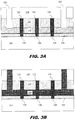
- FIGS. 2A and 2B are diagrams showing an illustrative process for forming dual-material nanowires with junctions below an edge of the gate layer, according to one example of principles described herein.
- FIGS. 3A and 3B are diagrams showing an illustrative process for replacing a dummy gate layer with a metal gate layer, according to one example of principles described herein.
- FIGS. 4A, 4B, 4C, and 4D are diagrams showing an illustrative process for forming polish-stop pillars to control heights of the nanowires, according to one example of principles described herein.
- FIG. 5 is a diagram showing polish-stop pillars having different heights, according to one example of principles described herein.
- FIGS. 6A, 6B, 6C, and 6D are diagrams showing an illustrative process for forming both N-type and P-type nanowires, according to one example of principles described herein.
- FIG. 7 is a flowchart showing an illustrative method for fabricating dual-material elongated semiconductor structures with substantially coplanar junctions, according to one example of principles described herein.
- first and second features are formed in direct contact
- additional features may be formed between the first and second features, such that the first and second features may not be in direct contact
- present disclosure may repeat reference numerals and/or letters in the various examples. This repetition is for the purpose of simplicity and clarity and does not in itself dictate a relationship between the various embodiments and/or configurations discussed.
- spatially relative terms such as “beneath,” “below,” “lower,” “above,” “upper” and the like, may be used herein for ease of description to describe one element or feature's relationship to another element(s) or feature(s) as illustrated in the figures.
- the spatially relative terms are intended to encompass different orientations of the device in use or operation in addition to the orientation depicted in the figures.
- the apparatus may be otherwise oriented (rotated 90 degrees or at other orientations) and the spatially relative descriptors used herein may likewise be interpreted accordingly.
- each of the nanowires may not be the same height after the epitaxial process is complete.
- the methods described herein disclose fabrication processes that produce nanowires with substantially similar heights.
- dual-material elongated semiconductor structures are formed on a substrate. Additionally, the junctions between the two different semiconductor materials of the elongated semiconductor structures are substantially co-planar.
- a first epitaxial process is used to form the lower portions of the elongated semiconductor structures. As described above, such epitaxial processes result in semiconductor structures having different heights.
- a gate layer is first deposited such that it covers each of the elongated semiconductor structures. Then, a planarization process, such as a chemical mechanical polishing (CMP) process, is performed such that the gate layer is reduced to a desired height.
- CMP chemical mechanical polishing
- planarization process reduces the height of each of the elongated semiconductor structures to match the height of the gate layer.
- each of the elongated gate structures as a similar height after the planarization process.
- the upper portions of the elongated semiconductor structures can then be formed on top of the lower portions using an epitaxial growth process.
- FIGS. 1A-1J are diagrams showing an illustrative process for forming nanowires with substantially similar heights.
- FIG. 1A illustrates a semiconductor substrate 102 and a patterned template layer 104 .
- the semiconductor substrate 102 may be made of a variety of semiconductor materials such as silicon, germanium, gallium arsenide, indium phosphide, and indium arsenide.
- the semiconductor substrate 102 is a semiconductor wafer.
- the template layer 104 may act as a template by exposing certain regions of the substrate 102 to an epitaxial growth process as will be described in further detail below.
- the template layer 104 may be made of a variety of materials. Such materials may be dielectric materials. Such materials may include, for example, silicon dioxide (SiO 2 ), silicon nitride (SiN x ), aluminum oxide (Al 2 O 3 ), hafnium oxide (HfO 2 ) or any combination thereof.
- the template layer 104 may be formed by first depositing the material onto the semiconductor substrate 102 . Then, the template layer 104 may be patterned using various photolithographic techniques. For example, a photoresist may be deposited and exposed to a light source using a photomask. Then, the photoresist may be developed such that the pattern exposes the underlying template layer 104 to an etching process.
- the template layer 104 may have a thickness within a range of about 2-40 nanometers (nm).
- FIG. 1B illustrates an epitaxial growth process 108 by which a plurality of elongated semiconductor structures 106 are formed.
- the elongated semiconductor structures 106 may be the lower portions of the full elongated semiconductor structures that will eventually be formed.
- An epitaxial growth process involves the formation of a crystal structure on a crystal substrate.
- the crystal substrate is the semiconductor substrate 102 .
- the crystal structures being formed are the elongated semiconductor structures 106 .
- the elongated semiconductor structures 106 grow only on the portions of the substrate 102 that are exposed through the template layer 104 .
- different structures may grow at different rates.
- the epitaxial process 108 is complete, the elongated semiconductor structures 106 may have varying heights.
- the elongated semiconductor structures 106 may be made of a variety of materials. Such materials may include, for example, silicon, germanium, silicon germanium, indium arsenide, indium gallium arsenide, indium antimonide, and indium gallium antimonide. Additionally, the elongated semiconductor structures 106 may be doped. The doping of the elongated semiconductor structures may occur in-situ. The type of dopant used is based on the type of transistor to be formed. Additionally, the in-situ doping can be changed as the epitaxial growth process 108 proceeds. For example, the in-situ doping can stop and restart as the epitaxial growth process 108 proceeds. In some cases, the doping profile may be graded.
- the doping profile may be stepped. Additionally, the in-situ doping can change dopant types during the epitaxial growth process 108 .
- the doping concentration of the elongated semiconductor structures 106 may be within a range of about 1 ⁇ 10 15 -5 ⁇ 10 20 cm 3 . In some examples, if the elongated semiconductor structures 106 include two different materials, such as silicon germanium, the ratio of one material to another may change gradually during the process. Thus, the concentration of the second material may have a graded profile. This may be done, for example, by changing flow rates of a precursor during the epitaxial growth process.
- the elongated semiconductor structures may be formed to have a variety of shapes from a top perspective.
- the elongated semiconductor structures 106 may be substantially circular or elliptical from a top perspective.
- the elongated semiconductor structures 106 may be substantially square or rectangular from a top perspective.
- the elongated semiconductor structures 106 may be substantially hexagonal in shape.
- the elongated semiconductor structures 106 may have an elongated shape from the top perspective. In such examples, the elongated semiconductor structures 106 may be referred to as nanobars.
- FIG. 1C is a diagram illustrating a dummy dielectric layer 110 formed over the substrate.
- the dummy dielectric layer 110 is deposited directly on the template layer 104 and directly on the elongated semiconductor structures 106 . Specifically, the dummy dielectric layer 110 is disposed on sidewalls of the elongated semiconductor structures as well as the top of the elongated semiconductor structures 106 .
- the dummy dielectric layer 110 may be made of a variety of dielectric materials, such as, silicon dioxide (SiO 2 ), silicon nitride (SiN x ), aluminum oxide (Al 2 O 3 ), hafnium oxide (HfO 2 ) or any combination thereof.
- FIG. 1D is a diagram showing illustrative deposition of the gate layer 112 .
- the gate layer 112 is a dummy gate layer that will later be replaced by a metal gate.
- to gate layer 112 may be made of polysilicon.
- the gate layer 112 is deposited such that it covers each of the elongated semiconductor structures 106 .
- FIG. 1E is a diagram showing an illustrative planarization process 114 that is used to planarize the surface of the gate layer 112 and the elongated semiconductor structures 106 .
- the planarization process 114 is a CMP process.
- a CMP process involves the use of a chemical slurry having abrasive particles suspended therein. The slurry is deposited onto the surface of the wafer and a polishing pad is used to polish the surface. The abrasive particles, along with the chemical solution, remove material to create a planar surface.
- the top surface of the gate layer 112 is substantially coplanar with the top surface of the elongated semiconductor structures 106 .
- the CMP process continues until the elongated semiconductor structures 106 have a final height.
- the elongated semiconductor structures 106 may have a final height within a range of about 5-150 nm.
- FIG. 1F illustrates a removal process 116 , such as an etching process, to create an offset between the elongated semiconductor structures 106 and the top of the gate layer 112 .
- the removal process 116 is selective such that it removes the gate layer 112 while leaving the elongated semiconductor structures 106 substantially intact.
- the removal process 116 may be a wet etching process or dry etching process.
- the removal process 116 reduces the height 118 of the gate layer 112 such that there is an offset 119 between the gate layer 112 in the top surfaces of the elongated gate structures 106 .
- a second material will be formed on top of the elongated semiconductor structures 106 .
- the offset 119 may be within a range of about 0-50 nm.
- FIG. 1G illustrates an additional epitaxial growth process 120 to form upper portions of elongated semiconductor structures 122 .
- the elongated semiconductor structures 122 are made of a different material than the elongated semiconductor structures 106 .
- the upper portions of the nanowires are made of a different material than the lower portion of the nanowires.
- the junctions 121 between the lower portions in the upper portions are substantially coplanar.
- each of the junctions 121 between the lower portions 106 in the upper portions 122 is at a substantially similar distance (i.e., offset) from the top surface of the gate layer 112 . This allows for better device performance and consistency.
- the epitaxial process 120 results in elongated semiconductor structures 122 having varying heights.
- the elongated semiconductor structures 122 may be made of a variety of materials. Such materials may include, for example, silicon, germanium, silicon germanium, indium arsenide, indium gallium arsenide, indium antimonide, and indium gallium antimonide. Additionally, the elongated semiconductor structures 122 may be doped. The doping of the elongated semiconductor structures may occur in-situ. The type of dopant used is based on the type of transistor to be formed. Additionally, the in-situ doping can be changed as the epitaxial growth process 120 proceeds. For example, the in-situ doping can stop and restart as the epitaxial growth process 120 proceeds. Additionally, the in-situ doping can change dopant types during the epitaxial growth process 120 . The doping concentration of the elongated semiconductor structures 122 may be within a range of about 1 ⁇ 10 15 -5 ⁇ 10 20 cm 3 .
- FIG. 1H illustrates deposition of the dielectric layer 124 .
- the dielectric layer 124 may also be referred to as a capping layer.
- the dielectric layer 124 is deposited such that it covers each of the elongated semiconductor structures 122 .
- FIG. 1I illustrates a planarization process 126 .
- the planarization process 126 may be, for example, a CMP process.
- the planarization process 126 planarizes the surface of the wafer so as to expose the top surfaces of each of the elongated semiconductor structures 122 .
- the height of each of the elongated semiconductor structures 122 is made substantially similar.
- FIG. 1J is a diagram illustrating deposition of an additional dielectric layer 128 .
- the additional dielectric layer 128 is an inter-layer dielectric (ILD) layer.
- ILD inter-layer dielectric
- various features may be formed into the additional dielectric layer 128 . Such features may include, for example, vias and contacts that connect the elongated semiconductor structures 122 to other components within the circuit.
- FIGS. 2A and 2B are diagrams showing an illustrative process for forming dual-material nanowires with junctions below an edge of the gate layer 112 .
- the offset 204 between the top surface of the gate layer 112 and the junctions between the lower portions 106 and upper portions 122 is negative.
- a removal process 202 is applied after the planarization process 114 is performed.
- the removal process 202 removes portions of the elongated semiconductor structures 106 while leaving the gate layer 112 substantially intact.
- the removal process 202 is applied for as long as it takes to remove the desired amount of material and create the desired offset 204 .
- the removal process may be a dry etch process or a wet etch process, for example.
- FIG. 2B illustrates an epitaxial growth process 206 to form the upper portions of the elongated semiconductor structures 106 .
- Epitaxial growth process 206 is similar to the epitaxial growth process 120 described above. Here, however, growth of the upper portions 122 starts at a point that is lower than the top surface of the gate layer 112 . The process then continues as described above in the text accompanying FIGS. 1H-1J .
- FIGS. 3A-3B are diagrams showing an illustrative process for replacing a dummy gate layer with a metal gate layer.
- replacement of the gate layer 112 occurs after placement of the additional dielectric layer 128 .
- replacement of the gate layer 112 may occur after the planarization process 126 and before the formation of the additional dielectric layer 128 .
- FIG. 3A illustrates formation of trenches 302 that extend down to the gate layer 112 .
- the trenches 302 extend through the additional dielectric layer 128 and the capping layer 124 .
- the trenches 302 may be formed in a variety of manners. For example, a patterned photoresist layer and/or hard mask layer may be deposited on the surface of the wafer. The regions of the wafer that are exposed through the photoresist layer or hard mask been exposed to an etching process.
- the etching process may be a dry etching process. A dry etching process is anisotropic and will thus etch downwards in a substantially straight manner.
- a wet etching process may be used to remove the gate layer 112 .
- a wet etching process is isotropic and thus can remove material in all directions. The wet etching may be selective so as to remove the gate layer 112 material (e.g., polysilicon), while leaving the remaining materials substantially intact.
- the dielectric layer 110 surrounding the elongated semiconductor structures 106 may be removed as well.
- FIG. 3B illustrates deposition of a metal material within the space left by the gate layer 112 .
- the metal material forms a metal gate layer 304 .
- the metal gate layer 304 functions as a gate for the transistors formed in part by the elongated semiconductor structures 106 , 122 . Additionally, the metal material within the trenches 302 may form a via to serve as a gate contact.
- the metal material used to form the metal gate layer 304 may be one of a variety of materials. For example, the metal material maybe tungsten.
- FIGS. 4A-4D are diagrams showing an illustrative process for forming polish-stop pillars 404 to control the heights of the nanowires.
- FIG. 4A illustrates a polish-stop layer 402 formed on top of the template layer 104 before the template layer is patterned. The thickness of the polish-stop layer 402 is such that the top of the polish-stop layer 402 corresponds to the desired height of the elongated semiconductor structures 106 .
- the polish-stop layer 402 may be made of a hard material that is resistant to a CMP process. One example of such material may be silicon nitride.
- FIG. 4B illustrates the stop layer 402 after it has been patterned to form stop pillars 404 .
- the polish-stop layer 402 may be patterned using various photolithographic techniques.
- the polish-stop pillars 404 may have a variety of shapes when viewed from a top perspective.
- the polish-stop pillars 404 may be square, rectangular, circular, elliptical, or may take other shapes.
- the polish-stop pillars 404 may vary in size as well.
- the polish-stop pillars 404 may be placed at regions where no other features, such as elongated semiconductor structures 106 , are to be placed.
- FIG. 4C illustrates formation of the elongated semiconductor structures 106 .
- the elongated semiconductor structures 106 may be formed as described above.
- FIG. 4D illustrates the planarized elongated semiconductor structures 106 after the planarization process 114 described above. Because the polish-stop pillars 404 are made of a material that is resistant to the CMP process, the CMP process will be prevented from moving forward once it reaches the top of the polish-stop pillars 404 . Thus, the polish-stop pillars 404 can be used to control the height of the elongated semiconductor structures 106 .
- FIG. 5 is a diagram showing polish-stop pillars 502 , 508 having different heights.
- polish-stop pillars 502 , 508 at different regions of a wafer may have different heights.
- polish-stop pillar 502 has a greater height than polish-stop pillar 508 .
- the elongated semiconductor structures 504 near polish-stop pillar 502 have a greater height than the elongated semiconductor structures 510 near polish-stop pillar 508 .
- FIGS. 6A-6D are diagrams showing an illustrative process for forming both N-type and P-type nanowires.
- Integrated circuits typically include both N-type and P-type transistors which together form complementary metal oxide semiconductor (CMOS) circuits.
- CMOS complementary metal oxide semiconductor
- N-type and P-type nanowire transistors may use different types of semiconductor material as well as being doped with different types of dopant.
- photoresist layer 602 and/or mask layer is used to cover a subset of the elongated semiconductor structures 106 as shown in FIG. 6A .
- the photoresist layer 602 may be applied after the planarization process 114 described above.
- the exposed subset of elongated semiconductor structures 106 may then be removed using an etching process 604 as illustrated in FIG. 6B .
- the etching process 604 may be selective so that it removes the elongated semiconductor structures 106 while leaving other materials, such as the gate layer 112 , substantially intact. Removal of the exposed elongated semiconductor structures 106 creates trenches 606 that expose the substrate 102 .
- FIG. 6C illustrates an epitaxial growth process 610 to grow elongated semiconductor structures 608 .
- the material used to form elongated semiconductor structures 608 is different than the material used to form the elongated semiconductor structures 106 .
- the material used to form the elongated semiconductor structures 608 is designed for a P-type transistor and the material used to form the elongated semiconductor structures 106 is designed for an N-type transistor.
- the elongated semiconductor structures 608 may be made of a variety of materials suited for P-type transistors. Additionally, the elongated semiconductor structures 608 may be doped. The doping of the elongated semiconductor structures 608 may occur in-situ. Additionally, the in-situ doping can be changed as the epitaxial growth process 108 proceeds. For example, the in-situ doping can stop and restart as the epitaxial growth process 108 proceeds. In some cases, the doping profile may be graded. In some examples, however, the doping profile may be stepped. The doping concentration of the elongated semiconductor structures 608 may be within a range of about 1 ⁇ 10 15 -5 ⁇ 10 20 cm 3 .
- the ratio of one material to another may change gradually during the process.
- the concentration of the second material may have a graded profile. This may be done, for example, by changing flow rates of a precursor during the epitaxial growth process.
- FIG. 6D illustrates a planarization process 612 to remove the photoresist 602 and/or hard mask layer as well as to planarize the elongated semiconductor structures 608 .
- the elongated semiconductor structures 106 and elongated semiconductor structures 608 will have the same height. That height corresponds to the top surface of the gate layer 112 .
- FIG. 7 is a flowchart showing an illustrative method for fabricating a dual-material elongated semiconductor structure with substantially coplanar junctions.
- the method 700 includes a step 702 for epitaxially growing first portions of a plurality of elongated semiconductor structures on a semiconductor substrate.
- the elongated semiconductor structures run perpendicular to the substrate. In other words, the elongated semiconductor structures are formed vertically.
- each of the elongated semiconductor structures may have a slightly different height after the epitaxial process is complete. It is desirable, however, that the top surfaces of each of the elongated semiconductor structures are substantially coplanar.
- the method 700 further includes a step 704 for forming a gate layer on the substrate.
- the gate layer contacts the elongated semiconductor structures.
- the gate layer fully covers each of the elongated semiconductor structures.
- the gate layer may be a dummy gate layer.
- the gate layer may be made of polysilicon that will eventually be replaced with a metal gate layer. Such a replacement process may occur after other processes that may adversely affect metal gate layer are performed.
- the method 700 further includes a step 706 for performing a planarization process on the gate layer and the elongated semiconductor structures.
- the planarization process may be, for example, a CMP process.
- the planarization process equalizes the height of each of the elongated semiconductor structures.
- the method 700 further includes a step 708 for epitaxially growing second portions of the plurality of elongated semiconductor structures.
- the second portions are made of a different semiconductor material than the first portions.
- the epitaxial process will cause the second portions (upper portions) to grow directly onto the exposed upper surfaces of the first portions (lower portions) of the elongated semiconductor structures.
- the combined lower portions and upper portions may be doped appropriately so they can function as part of a transistor.
- a method includes epitaxially growing first portions of a plurality of elongated semiconductor structures on a semiconductor substrate, the elongated semiconductor structures running perpendicular to the substrate. The method further includes forming a gate layer on the substrate, the gate layer contacting the elongated semiconductor structures. The method further includes performing a planarization process on the gate layer and the elongated semiconductor structures, and epitaxially growing second portions of the plurality of elongated semiconductor structures, the second portions comprising a different material than the first portions.
- a method includes forming a first set of elongated semiconductor structures on a semiconductor substrate, the first set of elongated semiconductor structures running perpendicular to the substrate. The method further includes forming a dummy gate layer on the substrate, the dummy gate layer contacting the first set of elongated semiconductor structures, performing a planarization process on the dummy gate layer and the first set of elongated semiconductor structures, and forming, a second set of elongated semiconductor structures on and aligned with the first set of elongated semiconductor structures, the second set of elongated semiconductor structures comprising a different material than the first set of elongated semiconductor structures.
- a semiconductor device includes a semiconductor substrate, a first set of elongated semiconductor structures extending from the semiconductor substrate in a direction that is perpendicular to the semiconductor substrate, and a second set of elongated semiconductor structures disposed directly on the first set of elongated semiconductor structures, the second set of elongated semiconductor structures comprising a different material than the first set of elongated semiconductor structures. Junctions between the first set of elongated semiconductor structures and the second set of elongated semiconductor structures are substantially coplanar.
Landscapes
- Engineering & Computer Science (AREA)
- Physics & Mathematics (AREA)
- Chemical & Material Sciences (AREA)
- Nanotechnology (AREA)
- Manufacturing & Machinery (AREA)
- Computer Hardware Design (AREA)
- Microelectronics & Electronic Packaging (AREA)
- Power Engineering (AREA)
- General Physics & Mathematics (AREA)
- Condensed Matter Physics & Semiconductors (AREA)
- Crystallography & Structural Chemistry (AREA)
- Mathematical Physics (AREA)
- Theoretical Computer Science (AREA)
- Insulated Gate Type Field-Effect Transistor (AREA)
- Metal-Oxide And Bipolar Metal-Oxide Semiconductor Integrated Circuits (AREA)
- Electrodes Of Semiconductors (AREA)
- Recrystallisation Techniques (AREA)
Abstract
Description
Claims (20)
Priority Applications (1)
| Application Number | Priority Date | Filing Date | Title |
|---|---|---|---|
| US16/179,645 US10861933B2 (en) | 2015-10-30 | 2018-11-02 | Elongated semiconductor structure planarization |
Applications Claiming Priority (2)
| Application Number | Priority Date | Filing Date | Title |
|---|---|---|---|
| US14/927,822 US10121858B2 (en) | 2015-10-30 | 2015-10-30 | Elongated semiconductor structure planarization |
| US16/179,645 US10861933B2 (en) | 2015-10-30 | 2018-11-02 | Elongated semiconductor structure planarization |
Related Parent Applications (1)
| Application Number | Title | Priority Date | Filing Date |
|---|---|---|---|
| US14/927,822 Division US10121858B2 (en) | 2015-10-30 | 2015-10-30 | Elongated semiconductor structure planarization |
Publications (2)
| Publication Number | Publication Date |
|---|---|
| US20190074355A1 US20190074355A1 (en) | 2019-03-07 |
| US10861933B2 true US10861933B2 (en) | 2020-12-08 |
Family
ID=58635832
Family Applications (2)
| Application Number | Title | Priority Date | Filing Date |
|---|---|---|---|
| US14/927,822 Active US10121858B2 (en) | 2015-10-30 | 2015-10-30 | Elongated semiconductor structure planarization |
| US16/179,645 Active 2036-02-10 US10861933B2 (en) | 2015-10-30 | 2018-11-02 | Elongated semiconductor structure planarization |
Family Applications Before (1)
| Application Number | Title | Priority Date | Filing Date |
|---|---|---|---|
| US14/927,822 Active US10121858B2 (en) | 2015-10-30 | 2015-10-30 | Elongated semiconductor structure planarization |
Country Status (3)
| Country | Link |
|---|---|
| US (2) | US10121858B2 (en) |
| CN (1) | CN106653564A (en) |
| TW (1) | TWI723054B (en) |
Families Citing this family (6)
| Publication number | Priority date | Publication date | Assignee | Title |
|---|---|---|---|---|
| EP3185299B1 (en) * | 2015-12-21 | 2023-05-24 | IMEC vzw | Self-alligned nanostructures for semi-conductor device |
| WO2017153193A1 (en) * | 2016-03-11 | 2017-09-14 | Imec Vzw | Method for providing a target layer surrounding a vertical nanostructure |
| US11018254B2 (en) | 2016-03-31 | 2021-05-25 | International Business Machines Corporation | Fabrication of vertical fin transistor with multiple threshold voltages |
| FR3053525B1 (en) * | 2016-06-29 | 2018-11-09 | Commissariat A L'energie Atomique Et Aux Energies Alternatives | METHOD FOR HOMOGENIZING THE HEIGHT OF A PLURALITY OF WIRES AND DEVICE MANUFACTURING METHOD USING SUCH WIRES |
| FR3053760B1 (en) * | 2016-07-05 | 2020-07-17 | Valeo Vision | LIGHT SOURCE AND CORRESPONDING LIGHT MODULE FOR A MOTOR VEHICLE |
| SG11202001177SA (en) * | 2017-09-05 | 2020-03-30 | Applied Materials Inc | Bottom-up approach to high aspect ratio hole formation in 3d memory structures |
Citations (55)
| Publication number | Priority date | Publication date | Assignee | Title |
|---|---|---|---|---|
| US5264387A (en) * | 1992-10-27 | 1993-11-23 | International Business Machines Corporation | Method of forming uniformly thin, isolated silicon mesas on an insulating substrate |
| US20050074972A1 (en) | 2003-10-03 | 2005-04-07 | Tomohiro Saito | Semiconductor device and method of manufacturing the same |
| US20050263795A1 (en) | 2004-05-25 | 2005-12-01 | Jeong-Dong Choi | Semiconductor device having a channel layer and method of manufacturing the same |
| US7425740B2 (en) | 2005-10-07 | 2008-09-16 | Taiwan Semiconductor Manufacturing Company, Ltd. | Method and structure for a 1T-RAM bit cell and macro |
| US20090001464A1 (en) | 2007-06-27 | 2009-01-01 | International Business Machines Corporation | Finfet with top body contact |
| US20090008631A1 (en) | 2006-01-25 | 2009-01-08 | Nxp B.V. | Nanowire tunneling transistor |
| US20090200540A1 (en) | 2008-02-07 | 2009-08-13 | Bjoerk Mikael T | Metal-Oxide-Semiconductor Device Including a Multiple-Layer Energy Filter |
| US7667271B2 (en) | 2007-04-27 | 2010-02-23 | Taiwan Semiconductor Manufacturing Company, Ltd. | Fin field-effect transistors |
| US20100270611A1 (en) | 2009-04-28 | 2010-10-28 | Fujio Masuoka | Semiconductor device including a mos transistor and production method therefor |
| US20110068407A1 (en) | 2009-09-24 | 2011-03-24 | Taiwan Semiconductor Manufacturing Company, Ltd. | Germanium FinFETs with Metal Gates and Stressors |
| US8048723B2 (en) | 2008-12-05 | 2011-11-01 | Taiwan Semiconductor Manufacturing Company, Ltd. | Germanium FinFETs having dielectric punch-through stoppers |
| US8053299B2 (en) | 2009-04-17 | 2011-11-08 | Taiwan Semiconductor Manufacturing Company, Ltd. | Method of fabrication of a FinFET element |
| US20120025169A1 (en) | 2010-08-02 | 2012-02-02 | Sundiode Inc. | Nanostructure array transistor |
| US8183627B2 (en) | 2004-12-01 | 2012-05-22 | Taiwan Semiconductor Manufacturing Company, Ltd. | Hybrid fin field-effect transistor structures and related methods |
| US20130011983A1 (en) | 2011-07-07 | 2013-01-10 | Taiwan Semiconductor Manufacturing Company, Ltd. | In-Situ Doping of Arsenic for Source and Drain Epitaxy |
| US8362575B2 (en) | 2009-09-29 | 2013-01-29 | Taiwan Semiconductor Manufacturing Company, Ltd. | Controlling the shape of source/drain regions in FinFETs |
| US8367498B2 (en) | 2010-10-18 | 2013-02-05 | Taiwan Semiconductor Manufacturing Company, Ltd. | Fin-like field effect transistor (FinFET) device and method of manufacturing same |
| US8415718B2 (en) | 2009-10-30 | 2013-04-09 | Taiwan Semiconductor Manufacturing Company, Ltd. | Method of forming epi film in substrate trench |
| US8440517B2 (en) | 2010-10-13 | 2013-05-14 | Taiwan Semiconductor Manufacturing Company, Ltd. | FinFET and method of fabricating the same |
| US8497177B1 (en) | 2012-10-04 | 2013-07-30 | Taiwan Semiconductor Manufacturing Company, Ltd. | Method of making a FinFET device |
| US8497528B2 (en) | 2010-05-06 | 2013-07-30 | Taiwan Semiconductor Manufacturing Company, Ltd. | Method for fabricating a strained structure |
| US20130285153A1 (en) | 2012-04-25 | 2013-10-31 | Taiwan Semiconductor Manufacturing Company Ltd. | Strained structure of semiconductor device and method of making the strained structure |
| US8609518B2 (en) | 2011-07-22 | 2013-12-17 | Taiwan Semiconductor Manufacturing Company, Ltd. | Re-growing source/drain regions from un-relaxed silicon layer |
| US8610240B2 (en) | 2009-10-16 | 2013-12-17 | Taiwan Semiconductor Manufacturing Company, Ltd. | Integrated circuit with multi recessed shallow trench isolation |
| US20130341733A1 (en) | 2012-06-25 | 2013-12-26 | International Business Machines Corporation | Plural Differential Pair Employing FinFET Structure |
| US8618556B2 (en) | 2011-06-30 | 2013-12-31 | Taiwan Semiconductor Manufacturing Company, Ltd. | FinFET design and method of fabricating same |
| US8633516B1 (en) | 2012-09-28 | 2014-01-21 | Taiwan Semiconductor Manufacturing Company, Ltd. | Source/drain stack stressor for semiconductor device |
| US20140070322A1 (en) | 2012-09-13 | 2014-03-13 | Globalfoundries Inc. | Methods of forming different finfet devices with different threshold voltages and integrated circuit products containing such devices |
| US8680576B2 (en) | 2012-05-16 | 2014-03-25 | Taiwan Semiconductor Manufacturing Company, Ltd. | CMOS device and method of forming the same |
| US8703565B2 (en) | 2010-02-09 | 2014-04-22 | Taiwan Semiconductor Manufacturing Company, Ltd. | Bottom-notched SiGe FinFET formation using condensation |
| US8723272B2 (en) | 2011-10-04 | 2014-05-13 | Taiwan Semiconductor Manufacturing Company, Ltd. | FinFET device and method of manufacturing same |
| US8729627B2 (en) | 2010-05-14 | 2014-05-20 | Taiwan Semiconductor Manufacturing Company, Ltd. | Strained channel integrated circuit devices |
| US8729634B2 (en) | 2012-06-15 | 2014-05-20 | Taiwan Semiconductor Manufacturing Company, Ltd. | FinFET with high mobility and strain channel |
| US8742509B2 (en) | 2012-03-01 | 2014-06-03 | Taiwan Semiconductor Manufacturing Company, Ltd. | Apparatus and method for FinFETs |
| US20140166981A1 (en) * | 2012-12-18 | 2014-06-19 | Brian S. Doyle | Vertical nanowire transistor with axially engineered semiconductor and gate metallization |
| US20140183600A1 (en) | 2012-12-28 | 2014-07-03 | Taiwan Semiconductor Manufacturing Company, Ltd. | Novel fin structure of finfet |
| US8776734B1 (en) | 2008-05-19 | 2014-07-15 | Innovative Environmental Solutions, Llc | Remedial system: a pollution control device for utilizing and abating volatile organic compounds |
| US8785285B2 (en) | 2012-03-08 | 2014-07-22 | Taiwan Semiconductor Manufacturing Company, Ltd. | Semiconductor devices and methods of manufacture thereof |
| US8796759B2 (en) | 2010-07-15 | 2014-08-05 | Taiwan Semiconductor Manufacturing Company, Ltd. | Fin-like field effect transistor (FinFET) device and method of manufacturing same |
| US8796666B1 (en) | 2013-04-26 | 2014-08-05 | Taiwan Semiconductor Manufacturing Company, Ltd. | MOS devices with strain buffer layer and methods of forming the same |
| US20140225184A1 (en) * | 2013-02-08 | 2014-08-14 | Taiwan Semiconductor Manufacturing Company, Ltd. | Method for Inducing Strain in Vertical Semiconductor Columns |
| US8809139B2 (en) | 2012-11-29 | 2014-08-19 | Taiwan Semiconductor Manufacturing Company, Ltd. | Fin-last FinFET and methods of forming same |
| US8815712B2 (en) | 2011-12-28 | 2014-08-26 | Taiwan Semiconductor Manufacturing Company, Ltd. | Method for epitaxial re-growth of semiconductor region |
| US8828823B2 (en) | 2011-10-13 | 2014-09-09 | Taiwan Semiconductor Manufacturing Company, Ltd. | FinFET device and method of manufacturing same |
| US20140252412A1 (en) | 2013-03-06 | 2014-09-11 | Taiwan Semiconductor Manufacturing Co., Ltd. | Strained and Uniform Doping Technique for FINFETs |
| US8836016B2 (en) | 2012-03-08 | 2014-09-16 | Taiwan Semiconductor Manufacturing Company, Ltd. | Semiconductor structures and methods with high mobility and high energy bandgap materials |
| US20140264590A1 (en) | 2013-03-13 | 2014-09-18 | Taiwan Semiconductor Manufacturing Company, Ltd. | FinFET with Bottom SiGe Layer in Source/Drain |
| US20140264592A1 (en) | 2013-03-12 | 2014-09-18 | Taiwan Semiconductor Manufacturing Co. Ltd. | Barrier Layer for FinFET Channels |
| US8841701B2 (en) | 2011-08-30 | 2014-09-23 | Taiwan Semiconductor Manufacturing Company, Ltd. | FinFET device having a channel defined in a diamond-like shape semiconductor structure |
| US8847293B2 (en) | 2012-03-02 | 2014-09-30 | Taiwan Semiconductor Manufacturing Company, Ltd. | Gate structure for semiconductor device |
| US8853025B2 (en) | 2013-02-08 | 2014-10-07 | Taiwan Semiconductor Manufacturing Company, Ltd. | FinFET/tri-gate channel doping for multiple threshold voltage tuning |
| US20150069475A1 (en) | 2013-09-12 | 2015-03-12 | Taiwan Semiconductor Manufacturing Company Limited | Semiconductor device with reduced electrical resistance and capacitance |
| TW201532274A (en) | 2014-02-07 | 2015-08-16 | 格羅方德半導體公司 | Fin field effect transistor having multi-layer fins for multi-turn logic application and method of forming same |
| US20150236092A1 (en) | 2014-02-19 | 2015-08-20 | Taiwan Semiconductor Manufacturing Company Limited | Semiconductor structures and methods for multi-level work function and multi-valued channel doping of nanowire transistors to improve drive current |
| US20160293739A1 (en) * | 2015-03-31 | 2016-10-06 | Stmicroelectronics, Inc. | Vertical gate-all-around tfet |
-
2015
- 2015-10-30 US US14/927,822 patent/US10121858B2/en active Active
-
2016
- 2016-10-20 TW TW105133922A patent/TWI723054B/en active
- 2016-10-26 CN CN201610946516.4A patent/CN106653564A/en active Pending
-
2018
- 2018-11-02 US US16/179,645 patent/US10861933B2/en active Active
Patent Citations (55)
| Publication number | Priority date | Publication date | Assignee | Title |
|---|---|---|---|---|
| US5264387A (en) * | 1992-10-27 | 1993-11-23 | International Business Machines Corporation | Method of forming uniformly thin, isolated silicon mesas on an insulating substrate |
| US20050074972A1 (en) | 2003-10-03 | 2005-04-07 | Tomohiro Saito | Semiconductor device and method of manufacturing the same |
| US20050263795A1 (en) | 2004-05-25 | 2005-12-01 | Jeong-Dong Choi | Semiconductor device having a channel layer and method of manufacturing the same |
| US8183627B2 (en) | 2004-12-01 | 2012-05-22 | Taiwan Semiconductor Manufacturing Company, Ltd. | Hybrid fin field-effect transistor structures and related methods |
| US7425740B2 (en) | 2005-10-07 | 2008-09-16 | Taiwan Semiconductor Manufacturing Company, Ltd. | Method and structure for a 1T-RAM bit cell and macro |
| US20090008631A1 (en) | 2006-01-25 | 2009-01-08 | Nxp B.V. | Nanowire tunneling transistor |
| US7667271B2 (en) | 2007-04-27 | 2010-02-23 | Taiwan Semiconductor Manufacturing Company, Ltd. | Fin field-effect transistors |
| US20090001464A1 (en) | 2007-06-27 | 2009-01-01 | International Business Machines Corporation | Finfet with top body contact |
| US20090200540A1 (en) | 2008-02-07 | 2009-08-13 | Bjoerk Mikael T | Metal-Oxide-Semiconductor Device Including a Multiple-Layer Energy Filter |
| US8776734B1 (en) | 2008-05-19 | 2014-07-15 | Innovative Environmental Solutions, Llc | Remedial system: a pollution control device for utilizing and abating volatile organic compounds |
| US8048723B2 (en) | 2008-12-05 | 2011-11-01 | Taiwan Semiconductor Manufacturing Company, Ltd. | Germanium FinFETs having dielectric punch-through stoppers |
| US8053299B2 (en) | 2009-04-17 | 2011-11-08 | Taiwan Semiconductor Manufacturing Company, Ltd. | Method of fabrication of a FinFET element |
| US20100270611A1 (en) | 2009-04-28 | 2010-10-28 | Fujio Masuoka | Semiconductor device including a mos transistor and production method therefor |
| US20110068407A1 (en) | 2009-09-24 | 2011-03-24 | Taiwan Semiconductor Manufacturing Company, Ltd. | Germanium FinFETs with Metal Gates and Stressors |
| US8362575B2 (en) | 2009-09-29 | 2013-01-29 | Taiwan Semiconductor Manufacturing Company, Ltd. | Controlling the shape of source/drain regions in FinFETs |
| US8610240B2 (en) | 2009-10-16 | 2013-12-17 | Taiwan Semiconductor Manufacturing Company, Ltd. | Integrated circuit with multi recessed shallow trench isolation |
| US8415718B2 (en) | 2009-10-30 | 2013-04-09 | Taiwan Semiconductor Manufacturing Company, Ltd. | Method of forming epi film in substrate trench |
| US8703565B2 (en) | 2010-02-09 | 2014-04-22 | Taiwan Semiconductor Manufacturing Company, Ltd. | Bottom-notched SiGe FinFET formation using condensation |
| US8497528B2 (en) | 2010-05-06 | 2013-07-30 | Taiwan Semiconductor Manufacturing Company, Ltd. | Method for fabricating a strained structure |
| US8729627B2 (en) | 2010-05-14 | 2014-05-20 | Taiwan Semiconductor Manufacturing Company, Ltd. | Strained channel integrated circuit devices |
| US8796759B2 (en) | 2010-07-15 | 2014-08-05 | Taiwan Semiconductor Manufacturing Company, Ltd. | Fin-like field effect transistor (FinFET) device and method of manufacturing same |
| US20120025169A1 (en) | 2010-08-02 | 2012-02-02 | Sundiode Inc. | Nanostructure array transistor |
| US8440517B2 (en) | 2010-10-13 | 2013-05-14 | Taiwan Semiconductor Manufacturing Company, Ltd. | FinFET and method of fabricating the same |
| US8367498B2 (en) | 2010-10-18 | 2013-02-05 | Taiwan Semiconductor Manufacturing Company, Ltd. | Fin-like field effect transistor (FinFET) device and method of manufacturing same |
| US8618556B2 (en) | 2011-06-30 | 2013-12-31 | Taiwan Semiconductor Manufacturing Company, Ltd. | FinFET design and method of fabricating same |
| US20130011983A1 (en) | 2011-07-07 | 2013-01-10 | Taiwan Semiconductor Manufacturing Company, Ltd. | In-Situ Doping of Arsenic for Source and Drain Epitaxy |
| US8609518B2 (en) | 2011-07-22 | 2013-12-17 | Taiwan Semiconductor Manufacturing Company, Ltd. | Re-growing source/drain regions from un-relaxed silicon layer |
| US8841701B2 (en) | 2011-08-30 | 2014-09-23 | Taiwan Semiconductor Manufacturing Company, Ltd. | FinFET device having a channel defined in a diamond-like shape semiconductor structure |
| US8723272B2 (en) | 2011-10-04 | 2014-05-13 | Taiwan Semiconductor Manufacturing Company, Ltd. | FinFET device and method of manufacturing same |
| US8828823B2 (en) | 2011-10-13 | 2014-09-09 | Taiwan Semiconductor Manufacturing Company, Ltd. | FinFET device and method of manufacturing same |
| US8815712B2 (en) | 2011-12-28 | 2014-08-26 | Taiwan Semiconductor Manufacturing Company, Ltd. | Method for epitaxial re-growth of semiconductor region |
| US8742509B2 (en) | 2012-03-01 | 2014-06-03 | Taiwan Semiconductor Manufacturing Company, Ltd. | Apparatus and method for FinFETs |
| US8847293B2 (en) | 2012-03-02 | 2014-09-30 | Taiwan Semiconductor Manufacturing Company, Ltd. | Gate structure for semiconductor device |
| US8836016B2 (en) | 2012-03-08 | 2014-09-16 | Taiwan Semiconductor Manufacturing Company, Ltd. | Semiconductor structures and methods with high mobility and high energy bandgap materials |
| US8785285B2 (en) | 2012-03-08 | 2014-07-22 | Taiwan Semiconductor Manufacturing Company, Ltd. | Semiconductor devices and methods of manufacture thereof |
| US20130285153A1 (en) | 2012-04-25 | 2013-10-31 | Taiwan Semiconductor Manufacturing Company Ltd. | Strained structure of semiconductor device and method of making the strained structure |
| US8680576B2 (en) | 2012-05-16 | 2014-03-25 | Taiwan Semiconductor Manufacturing Company, Ltd. | CMOS device and method of forming the same |
| US8729634B2 (en) | 2012-06-15 | 2014-05-20 | Taiwan Semiconductor Manufacturing Company, Ltd. | FinFET with high mobility and strain channel |
| US20130341733A1 (en) | 2012-06-25 | 2013-12-26 | International Business Machines Corporation | Plural Differential Pair Employing FinFET Structure |
| US20140070322A1 (en) | 2012-09-13 | 2014-03-13 | Globalfoundries Inc. | Methods of forming different finfet devices with different threshold voltages and integrated circuit products containing such devices |
| US8633516B1 (en) | 2012-09-28 | 2014-01-21 | Taiwan Semiconductor Manufacturing Company, Ltd. | Source/drain stack stressor for semiconductor device |
| US8497177B1 (en) | 2012-10-04 | 2013-07-30 | Taiwan Semiconductor Manufacturing Company, Ltd. | Method of making a FinFET device |
| US8809139B2 (en) | 2012-11-29 | 2014-08-19 | Taiwan Semiconductor Manufacturing Company, Ltd. | Fin-last FinFET and methods of forming same |
| US20140166981A1 (en) * | 2012-12-18 | 2014-06-19 | Brian S. Doyle | Vertical nanowire transistor with axially engineered semiconductor and gate metallization |
| US20140183600A1 (en) | 2012-12-28 | 2014-07-03 | Taiwan Semiconductor Manufacturing Company, Ltd. | Novel fin structure of finfet |
| US20140225184A1 (en) * | 2013-02-08 | 2014-08-14 | Taiwan Semiconductor Manufacturing Company, Ltd. | Method for Inducing Strain in Vertical Semiconductor Columns |
| US8853025B2 (en) | 2013-02-08 | 2014-10-07 | Taiwan Semiconductor Manufacturing Company, Ltd. | FinFET/tri-gate channel doping for multiple threshold voltage tuning |
| US20140252412A1 (en) | 2013-03-06 | 2014-09-11 | Taiwan Semiconductor Manufacturing Co., Ltd. | Strained and Uniform Doping Technique for FINFETs |
| US20140264592A1 (en) | 2013-03-12 | 2014-09-18 | Taiwan Semiconductor Manufacturing Co. Ltd. | Barrier Layer for FinFET Channels |
| US20140264590A1 (en) | 2013-03-13 | 2014-09-18 | Taiwan Semiconductor Manufacturing Company, Ltd. | FinFET with Bottom SiGe Layer in Source/Drain |
| US8796666B1 (en) | 2013-04-26 | 2014-08-05 | Taiwan Semiconductor Manufacturing Company, Ltd. | MOS devices with strain buffer layer and methods of forming the same |
| US20150069475A1 (en) | 2013-09-12 | 2015-03-12 | Taiwan Semiconductor Manufacturing Company Limited | Semiconductor device with reduced electrical resistance and capacitance |
| TW201532274A (en) | 2014-02-07 | 2015-08-16 | 格羅方德半導體公司 | Fin field effect transistor having multi-layer fins for multi-turn logic application and method of forming same |
| US20150236092A1 (en) | 2014-02-19 | 2015-08-20 | Taiwan Semiconductor Manufacturing Company Limited | Semiconductor structures and methods for multi-level work function and multi-valued channel doping of nanowire transistors to improve drive current |
| US20160293739A1 (en) * | 2015-03-31 | 2016-10-06 | Stmicroelectronics, Inc. | Vertical gate-all-around tfet |
Non-Patent Citations (3)
| Title |
|---|
| USPTO, Patent Application and Drawings; U.S. Appl. No. 14/554,584, filed Nov. 26, 2014, entitled: Graded Heterojunction Nanowire Device, with Filing Receipt dated Jan. 23, 2015, 37 pages. |
| USPTO, U.S. Appl. No. 14/567,252, filed Dec. 11, 2014, Application, Drawings, Filing Receipt, 68 Pages. |
| USPTO, U.S. Appl. No. 14/640,295, filed Mar. 6, 2015, Application, Drawings, Filing Receipt, 62 Pages. |
Also Published As
| Publication number | Publication date |
|---|---|
| TW201715580A (en) | 2017-05-01 |
| US10121858B2 (en) | 2018-11-06 |
| TWI723054B (en) | 2021-04-01 |
| US20190074355A1 (en) | 2019-03-07 |
| CN106653564A (en) | 2017-05-10 |
| US20170125518A1 (en) | 2017-05-04 |
Similar Documents
| Publication | Publication Date | Title |
|---|---|---|
| US10861933B2 (en) | Elongated semiconductor structure planarization | |
| US11004946B2 (en) | FinFET structure with composite gate helmet | |
| US11569230B2 (en) | Method and structure for FinFET devices | |
| US20200266110A1 (en) | Structure and formation method of fin-like field effect transistor | |
| US10037921B2 (en) | Structure and formation method of fin-like field effect transistor | |
| US9564431B2 (en) | Semiconductor structures and methods for multi-level work function | |
| US12107165B2 (en) | Semiconductor device structure with cap layer | |
| US10340190B2 (en) | Semiconductor device structure and method for forming the same | |
| US9620422B2 (en) | Semiconductor arrangement | |
| US10707331B2 (en) | FinFET device with a reduced width | |
| US10276664B2 (en) | Semiconductor structures and methods for multi-dimension of nanowire diameter to improve drive current | |
| US10714615B2 (en) | Method and structure for FinFET devices | |
| US12087771B2 (en) | Multiple patterning gate scheme for nanosheet rule scaling | |
| US9659826B2 (en) | Asymmetric source/drain depths | |
| US20250318189A1 (en) | Asymmetric Source/Drain for Backside Source Contact | |
| US9634132B2 (en) | Semiconductor structures and methods for multi-level band gap energy of nanowire transistors to improve drive current | |
| US20240363629A1 (en) | Finfet pitch scaling |
Legal Events
| Date | Code | Title | Description |
|---|---|---|---|
| AS | Assignment |
Owner name: TAIWAN SEMICONDUCTOR MANUFACTURING COMPANY., LTD., Free format text: ASSIGNMENT OF ASSIGNORS INTEREST;ASSIGNORS:OXLAND, RICHARD KENNETH;DURIEZ, BLANDINE;DAL, MARK VAN;AND OTHERS;SIGNING DATES FROM 20151103 TO 20151105;REEL/FRAME:047399/0154 Owner name: TAIWAN SEMICONDUCTOR MANUFACTURING COMPANY., LTD., TAIWAN Free format text: ASSIGNMENT OF ASSIGNORS INTEREST;ASSIGNORS:OXLAND, RICHARD KENNETH;DURIEZ, BLANDINE;DAL, MARK VAN;AND OTHERS;SIGNING DATES FROM 20151103 TO 20151105;REEL/FRAME:047399/0154 |
|
| FEPP | Fee payment procedure |
Free format text: ENTITY STATUS SET TO UNDISCOUNTED (ORIGINAL EVENT CODE: BIG.); ENTITY STATUS OF PATENT OWNER: LARGE ENTITY |
|
| STPP | Information on status: patent application and granting procedure in general |
Free format text: DOCKETED NEW CASE - READY FOR EXAMINATION |
|
| STPP | Information on status: patent application and granting procedure in general |
Free format text: NON FINAL ACTION MAILED |
|
| STPP | Information on status: patent application and granting procedure in general |
Free format text: RESPONSE TO NON-FINAL OFFICE ACTION ENTERED AND FORWARDED TO EXAMINER |
|
| STPP | Information on status: patent application and granting procedure in general |
Free format text: NOTICE OF ALLOWANCE MAILED -- APPLICATION RECEIVED IN OFFICE OF PUBLICATIONS |
|
| STPP | Information on status: patent application and granting procedure in general |
Free format text: PUBLICATIONS -- ISSUE FEE PAYMENT VERIFIED |
|
| STCF | Information on status: patent grant |
Free format text: PATENTED CASE |
|
| MAFP | Maintenance fee payment |
Free format text: PAYMENT OF MAINTENANCE FEE, 4TH YEAR, LARGE ENTITY (ORIGINAL EVENT CODE: M1551); ENTITY STATUS OF PATENT OWNER: LARGE ENTITY Year of fee payment: 4 |