US10861867B2 - Memory device with reduced capacitance - Google Patents
Memory device with reduced capacitance Download PDFInfo
- Publication number
- US10861867B2 US10861867B2 US16/021,550 US201816021550A US10861867B2 US 10861867 B2 US10861867 B2 US 10861867B2 US 201816021550 A US201816021550 A US 201816021550A US 10861867 B2 US10861867 B2 US 10861867B2
- Authority
- US
- United States
- Prior art keywords
- dielectric
- wordlines
- memory
- memory array
- pillars
- Prior art date
- Legal status (The legal status is an assumption and is not a legal conclusion. Google has not performed a legal analysis and makes no representation as to the accuracy of the status listed.)
- Active
Links
Images


Classifications
-
- H01L27/11582—
-
- H—ELECTRICITY
- H10—SEMICONDUCTOR DEVICES; ELECTRIC SOLID-STATE DEVICES NOT OTHERWISE PROVIDED FOR
- H10B—ELECTRONIC MEMORY DEVICES
- H10B43/00—EEPROM devices comprising charge-trapping gate insulators
- H10B43/20—EEPROM devices comprising charge-trapping gate insulators characterised by three-dimensional [3D] arrangements, e.g. with cells on different height levels
- H10B43/23—EEPROM devices comprising charge-trapping gate insulators characterised by three-dimensional [3D] arrangements, e.g. with cells on different height levels with source and drain on different levels, e.g. with sloping channels
- H10B43/27—EEPROM devices comprising charge-trapping gate insulators characterised by three-dimensional [3D] arrangements, e.g. with cells on different height levels with source and drain on different levels, e.g. with sloping channels the channels comprising vertical portions, e.g. U-shaped channels
-
- H01L21/7682—
-
- H01L23/528—
-
- H01L23/5329—
-
- H01L29/40117—
-
- H01L29/4916—
-
- H01L29/495—
-
- H01L29/513—
-
- H01L29/518—
-
- H01L29/66833—
-
- H01L29/7926—
-
- H—ELECTRICITY
- H10—SEMICONDUCTOR DEVICES; ELECTRIC SOLID-STATE DEVICES NOT OTHERWISE PROVIDED FOR
- H10D—INORGANIC ELECTRIC SEMICONDUCTOR DEVICES
- H10D30/00—Field-effect transistors [FET]
- H10D30/01—Manufacture or treatment
- H10D30/021—Manufacture or treatment of FETs having insulated gates [IGFET]
- H10D30/0413—Manufacture or treatment of FETs having insulated gates [IGFET] of FETs having charge-trapping gate insulators, e.g. MNOS transistors
-
- H—ELECTRICITY
- H10—SEMICONDUCTOR DEVICES; ELECTRIC SOLID-STATE DEVICES NOT OTHERWISE PROVIDED FOR
- H10D—INORGANIC ELECTRIC SEMICONDUCTOR DEVICES
- H10D30/00—Field-effect transistors [FET]
- H10D30/60—Insulated-gate field-effect transistors [IGFET]
- H10D30/69—IGFETs having charge trapping gate insulators, e.g. MNOS transistors
- H10D30/693—Vertical IGFETs having charge trapping gate insulators
-
- H—ELECTRICITY
- H10—SEMICONDUCTOR DEVICES; ELECTRIC SOLID-STATE DEVICES NOT OTHERWISE PROVIDED FOR
- H10D—INORGANIC ELECTRIC SEMICONDUCTOR DEVICES
- H10D64/00—Electrodes of devices having potential barriers
- H10D64/01—Manufacture or treatment
- H10D64/031—Manufacture or treatment of data-storage electrodes
- H10D64/037—Manufacture or treatment of data-storage electrodes comprising charge-trapping insulators
-
- H—ELECTRICITY
- H10—SEMICONDUCTOR DEVICES; ELECTRIC SOLID-STATE DEVICES NOT OTHERWISE PROVIDED FOR
- H10D—INORGANIC ELECTRIC SEMICONDUCTOR DEVICES
- H10D64/00—Electrodes of devices having potential barriers
- H10D64/60—Electrodes characterised by their materials
- H10D64/66—Electrodes having a conductor capacitively coupled to a semiconductor by an insulator, e.g. MIS electrodes
- H10D64/661—Electrodes having a conductor capacitively coupled to a semiconductor by an insulator, e.g. MIS electrodes the conductor comprising a layer of silicon contacting the insulator, e.g. polysilicon having vertical doping variation
-
- H—ELECTRICITY
- H10—SEMICONDUCTOR DEVICES; ELECTRIC SOLID-STATE DEVICES NOT OTHERWISE PROVIDED FOR
- H10D—INORGANIC ELECTRIC SEMICONDUCTOR DEVICES
- H10D64/00—Electrodes of devices having potential barriers
- H10D64/60—Electrodes characterised by their materials
- H10D64/66—Electrodes having a conductor capacitively coupled to a semiconductor by an insulator, e.g. MIS electrodes
- H10D64/665—Electrodes having a conductor capacitively coupled to a semiconductor by an insulator, e.g. MIS electrodes the conductor comprising a layer of elemental metal contacting the insulator, e.g. tungsten or molybdenum
-
- H—ELECTRICITY
- H10—SEMICONDUCTOR DEVICES; ELECTRIC SOLID-STATE DEVICES NOT OTHERWISE PROVIDED FOR
- H10D—INORGANIC ELECTRIC SEMICONDUCTOR DEVICES
- H10D64/00—Electrodes of devices having potential barriers
- H10D64/60—Electrodes characterised by their materials
- H10D64/66—Electrodes having a conductor capacitively coupled to a semiconductor by an insulator, e.g. MIS electrodes
- H10D64/68—Electrodes having a conductor capacitively coupled to a semiconductor by an insulator, e.g. MIS electrodes characterised by the insulator, e.g. by the gate insulator
- H10D64/681—Electrodes having a conductor capacitively coupled to a semiconductor by an insulator, e.g. MIS electrodes characterised by the insulator, e.g. by the gate insulator having a compositional variation, e.g. multilayered
- H10D64/685—Electrodes having a conductor capacitively coupled to a semiconductor by an insulator, e.g. MIS electrodes characterised by the insulator, e.g. by the gate insulator having a compositional variation, e.g. multilayered being perpendicular to the channel plane
-
- H—ELECTRICITY
- H10—SEMICONDUCTOR DEVICES; ELECTRIC SOLID-STATE DEVICES NOT OTHERWISE PROVIDED FOR
- H10D—INORGANIC ELECTRIC SEMICONDUCTOR DEVICES
- H10D64/00—Electrodes of devices having potential barriers
- H10D64/60—Electrodes characterised by their materials
- H10D64/66—Electrodes having a conductor capacitively coupled to a semiconductor by an insulator, e.g. MIS electrodes
- H10D64/68—Electrodes having a conductor capacitively coupled to a semiconductor by an insulator, e.g. MIS electrodes characterised by the insulator, e.g. by the gate insulator
- H10D64/693—Electrodes having a conductor capacitively coupled to a semiconductor by an insulator, e.g. MIS electrodes characterised by the insulator, e.g. by the gate insulator the insulator comprising nitrogen, e.g. nitrides, oxynitrides or nitrogen-doped materials
-
- H—ELECTRICITY
- H10—SEMICONDUCTOR DEVICES; ELECTRIC SOLID-STATE DEVICES NOT OTHERWISE PROVIDED FOR
- H10W—GENERIC PACKAGES, INTERCONNECTIONS, CONNECTORS OR OTHER CONSTRUCTIONAL DETAILS OF DEVICES COVERED BY CLASS H10
- H10W20/00—Interconnections in chips, wafers or substrates
- H10W20/01—Manufacture or treatment
- H10W20/071—Manufacture or treatment of dielectric parts thereof
- H10W20/072—Manufacture or treatment of dielectric parts thereof of dielectric parts comprising air gaps
-
- H—ELECTRICITY
- H10—SEMICONDUCTOR DEVICES; ELECTRIC SOLID-STATE DEVICES NOT OTHERWISE PROVIDED FOR
- H10W—GENERIC PACKAGES, INTERCONNECTIONS, CONNECTORS OR OTHER CONSTRUCTIONAL DETAILS OF DEVICES COVERED BY CLASS H10
- H10W20/00—Interconnections in chips, wafers or substrates
- H10W20/40—Interconnections external to wafers or substrates, e.g. back-end-of-line [BEOL] metallisations or vias connecting to gate electrodes
- H10W20/41—Interconnections external to wafers or substrates, e.g. back-end-of-line [BEOL] metallisations or vias connecting to gate electrodes characterised by their conductive parts
- H10W20/43—Layouts of interconnections
-
- H—ELECTRICITY
- H10—SEMICONDUCTOR DEVICES; ELECTRIC SOLID-STATE DEVICES NOT OTHERWISE PROVIDED FOR
- H10W—GENERIC PACKAGES, INTERCONNECTIONS, CONNECTORS OR OTHER CONSTRUCTIONAL DETAILS OF DEVICES COVERED BY CLASS H10
- H10W20/00—Interconnections in chips, wafers or substrates
- H10W20/40—Interconnections external to wafers or substrates, e.g. back-end-of-line [BEOL] metallisations or vias connecting to gate electrodes
- H10W20/45—Interconnections external to wafers or substrates, e.g. back-end-of-line [BEOL] metallisations or vias connecting to gate electrodes characterised by their insulating parts
- H10W20/46—Interconnections external to wafers or substrates, e.g. back-end-of-line [BEOL] metallisations or vias connecting to gate electrodes characterised by their insulating parts comprising air gaps
-
- H—ELECTRICITY
- H10—SEMICONDUCTOR DEVICES; ELECTRIC SOLID-STATE DEVICES NOT OTHERWISE PROVIDED FOR
- H10W—GENERIC PACKAGES, INTERCONNECTIONS, CONNECTORS OR OTHER CONSTRUCTIONAL DETAILS OF DEVICES COVERED BY CLASS H10
- H10W20/00—Interconnections in chips, wafers or substrates
- H10W20/40—Interconnections external to wafers or substrates, e.g. back-end-of-line [BEOL] metallisations or vias connecting to gate electrodes
- H10W20/45—Interconnections external to wafers or substrates, e.g. back-end-of-line [BEOL] metallisations or vias connecting to gate electrodes characterised by their insulating parts
- H10W20/48—Insulating materials thereof
-
- H01L21/0217—
-
- H01L21/02271—
-
- H01L21/3065—
-
- H01L21/31053—
-
- H01L21/32133—
-
- H01L2224/16225—
-
- H01L24/16—
-
- H01L29/66545—
-
- H01L2924/1438—
-
- H01L2924/14511—
-
- H—ELECTRICITY
- H10—SEMICONDUCTOR DEVICES; ELECTRIC SOLID-STATE DEVICES NOT OTHERWISE PROVIDED FOR
- H10D—INORGANIC ELECTRIC SEMICONDUCTOR DEVICES
- H10D64/00—Electrodes of devices having potential barriers
- H10D64/01—Manufacture or treatment
- H10D64/017—Manufacture or treatment using dummy gates in processes wherein at least parts of the final gates are self-aligned to the dummy gates, i.e. replacement gate processes
-
- H—ELECTRICITY
- H10—SEMICONDUCTOR DEVICES; ELECTRIC SOLID-STATE DEVICES NOT OTHERWISE PROVIDED FOR
- H10P—GENERIC PROCESSES OR APPARATUS FOR THE MANUFACTURE OR TREATMENT OF DEVICES COVERED BY CLASS H10
- H10P14/00—Formation of materials, e.g. in the shape of layers or pillars
- H10P14/60—Formation of materials, e.g. in the shape of layers or pillars of insulating materials
- H10P14/63—Formation of materials, e.g. in the shape of layers or pillars of insulating materials characterised by the formation processes
- H10P14/6326—Deposition processes
- H10P14/6328—Deposition from the gas or vapour phase
- H10P14/6334—Deposition from the gas or vapour phase using decomposition or reaction of gaseous or vapour phase compounds, i.e. chemical vapour deposition
-
- H—ELECTRICITY
- H10—SEMICONDUCTOR DEVICES; ELECTRIC SOLID-STATE DEVICES NOT OTHERWISE PROVIDED FOR
- H10P—GENERIC PROCESSES OR APPARATUS FOR THE MANUFACTURE OR TREATMENT OF DEVICES COVERED BY CLASS H10
- H10P14/00—Formation of materials, e.g. in the shape of layers or pillars
- H10P14/60—Formation of materials, e.g. in the shape of layers or pillars of insulating materials
- H10P14/69—Inorganic materials
- H10P14/694—Inorganic materials composed of nitrides
- H10P14/6943—Inorganic materials composed of nitrides containing silicon
- H10P14/69433—Inorganic materials composed of nitrides containing silicon the material being a silicon nitride not containing oxygen, e.g. SixNy or SixByNz
-
- H—ELECTRICITY
- H10—SEMICONDUCTOR DEVICES; ELECTRIC SOLID-STATE DEVICES NOT OTHERWISE PROVIDED FOR
- H10P—GENERIC PROCESSES OR APPARATUS FOR THE MANUFACTURE OR TREATMENT OF DEVICES COVERED BY CLASS H10
- H10P50/00—Etching of wafers, substrates or parts of devices
- H10P50/20—Dry etching; Plasma etching; Reactive-ion etching
- H10P50/24—Dry etching; Plasma etching; Reactive-ion etching of semiconductor materials
- H10P50/242—Dry etching; Plasma etching; Reactive-ion etching of semiconductor materials of Group IV materials
-
- H—ELECTRICITY
- H10—SEMICONDUCTOR DEVICES; ELECTRIC SOLID-STATE DEVICES NOT OTHERWISE PROVIDED FOR
- H10P—GENERIC PROCESSES OR APPARATUS FOR THE MANUFACTURE OR TREATMENT OF DEVICES COVERED BY CLASS H10
- H10P50/00—Etching of wafers, substrates or parts of devices
- H10P50/20—Dry etching; Plasma etching; Reactive-ion etching
- H10P50/26—Dry etching; Plasma etching; Reactive-ion etching of conductive or resistive materials
- H10P50/264—Dry etching; Plasma etching; Reactive-ion etching of conductive or resistive materials by chemical means
-
- H—ELECTRICITY
- H10—SEMICONDUCTOR DEVICES; ELECTRIC SOLID-STATE DEVICES NOT OTHERWISE PROVIDED FOR
- H10P—GENERIC PROCESSES OR APPARATUS FOR THE MANUFACTURE OR TREATMENT OF DEVICES COVERED BY CLASS H10
- H10P95/00—Generic processes or apparatus for manufacture or treatments not covered by the other groups of this subclass
- H10P95/06—Planarisation of inorganic insulating materials
- H10P95/062—Planarisation of inorganic insulating materials involving a dielectric removal step
-
- H—ELECTRICITY
- H10—SEMICONDUCTOR DEVICES; ELECTRIC SOLID-STATE DEVICES NOT OTHERWISE PROVIDED FOR
- H10W—GENERIC PACKAGES, INTERCONNECTIONS, CONNECTORS OR OTHER CONSTRUCTIONAL DETAILS OF DEVICES COVERED BY CLASS H10
- H10W72/00—Interconnections or connectors in packages
- H10W72/20—Bump connectors, e.g. solder bumps or copper pillars; Dummy bumps; Thermal bumps
-
- H—ELECTRICITY
- H10—SEMICONDUCTOR DEVICES; ELECTRIC SOLID-STATE DEVICES NOT OTHERWISE PROVIDED FOR
- H10W—GENERIC PACKAGES, INTERCONNECTIONS, CONNECTORS OR OTHER CONSTRUCTIONAL DETAILS OF DEVICES COVERED BY CLASS H10
- H10W74/00—Encapsulations, e.g. protective coatings
- H10W74/10—Encapsulations, e.g. protective coatings characterised by their shape or disposition
- H10W74/15—Encapsulations, e.g. protective coatings characterised by their shape or disposition on active surfaces of flip-chip devices, e.g. underfills
-
- H—ELECTRICITY
- H10—SEMICONDUCTOR DEVICES; ELECTRIC SOLID-STATE DEVICES NOT OTHERWISE PROVIDED FOR
- H10W—GENERIC PACKAGES, INTERCONNECTIONS, CONNECTORS OR OTHER CONSTRUCTIONAL DETAILS OF DEVICES COVERED BY CLASS H10
- H10W90/00—Package configurations
- H10W90/701—Package configurations characterised by the relative positions of pads or connectors relative to package parts
- H10W90/721—Package configurations characterised by the relative positions of pads or connectors relative to package parts of bump connectors
- H10W90/724—Package configurations characterised by the relative positions of pads or connectors relative to package parts of bump connectors between a chip and a stacked insulating package substrate, interposer or RDL
-
- H—ELECTRICITY
- H10—SEMICONDUCTOR DEVICES; ELECTRIC SOLID-STATE DEVICES NOT OTHERWISE PROVIDED FOR
- H10W—GENERIC PACKAGES, INTERCONNECTIONS, CONNECTORS OR OTHER CONSTRUCTIONAL DETAILS OF DEVICES COVERED BY CLASS H10
- H10W90/00—Package configurations
- H10W90/701—Package configurations characterised by the relative positions of pads or connectors relative to package parts
- H10W90/731—Package configurations characterised by the relative positions of pads or connectors relative to package parts of die-attach connectors
- H10W90/734—Package configurations characterised by the relative positions of pads or connectors relative to package parts of die-attach connectors between a chip and a stacked insulating package substrate, interposer or RDL
-
- H—ELECTRICITY
- H10—SEMICONDUCTOR DEVICES; ELECTRIC SOLID-STATE DEVICES NOT OTHERWISE PROVIDED FOR
- H10W—GENERIC PACKAGES, INTERCONNECTIONS, CONNECTORS OR OTHER CONSTRUCTIONAL DETAILS OF DEVICES COVERED BY CLASS H10
- H10W90/00—Package configurations
- H10W90/701—Package configurations characterised by the relative positions of pads or connectors relative to package parts
- H10W90/751—Package configurations characterised by the relative positions of pads or connectors relative to package parts of bond wires
- H10W90/754—Package configurations characterised by the relative positions of pads or connectors relative to package parts of bond wires between a chip and a stacked insulating package substrate, interposer or RDL
Definitions
- Embodiments of the present disclosure generally relate to the field of integrated circuits (IC), and more particularly, to fabrication techniques for a non-volatile memory device with reduced capacitance.
- IC integrated circuits
- a typical flash memory device may comprise a memory array that includes a large number of non-volatile memory cells arranged in row and column fashion.
- vertical memory such as three-dimensional (3D) memory
- 3D flash memory array may include a plurality of memory cells stacked over one another. Each group of memory cells may share a plurality of access lines, known as wordlines (WLs) and bitlines (BLs).
- wordline capacitance is a key parameter that determines product performance.
- the wordlines comprise a larger conductive sheet separated by thin dielectrics.
- wordlines in a 3D NAND array may be separated by continuous dielectric like SiO2. Having a large wordline area that includes multiple dielectric separation layers may result in a large capacitance in the memory array. This large capacitance may add significant delay in the array performance, which may be manifested in slower read and write speed.
- FIG. 1 illustrates an example die in which a memory device may be provided using the techniques of the present disclosure, in accordance with some embodiments.
- FIG. 2 schematically illustrates a cross-section side view of an integrated circuit (IC) assembly that includes a memory device provided using the techniques of the present disclosure, in accordance with some embodiments.
- IC integrated circuit
- FIGS. 3-14 illustrate example processes of forming a memory device with reduced capacitance, in accordance with some embodiments.
- FIG. 15 is a process flow diagram for providing a memory device with reduced capacitance, in accordance with some embodiments.
- FIG. 16 schematically illustrates an example computing device including a memory device with reduced capacitance, in accordance with some embodiments.
- Embodiments of the present disclosure describe techniques and configurations for a memory device comprising a memory array with reduced capacitance.
- the memory array is formed in a die, and includes one or more pillars and a plurality of wordlines coupled with the one or more pillars. Adjacent wordlines of the plurality of wordlines are separated by respective dielectric layers, which may include components, to reduce capacitance of the plurality of wordlines.
- the components comprise air gaps or low-k dielectric material.
- phrase “A and/or B” means (A), (B), (A) or (B), or (A and B).
- phrase “A, B, and/or C” means (A), (B), (C), (A and B), (A and C), (B and C), or (A, B and C).
- Coupled may mean one or more of the following. “Coupled” may mean that two or more elements are in direct physical or electrical contact. However, “coupled” may also mean that two or more elements indirectly contact each other, but yet still cooperate or interact with each other, and may mean that one or more other elements are coupled or connected between the elements that are said to be coupled with each other.
- directly coupled may mean that two or more elements are in direct contact.
- FIG. 1 illustrates an example die in which a memory device may be provided using the techniques of the present disclosure, in accordance with some embodiments. More specifically, FIG. 1 schematically illustrates a top view of die 102 in wafer form 10 and in singulated form 140 , in accordance with some embodiments.
- the die 102 may be one of a plurality of dies (e.g., die 102 , 102 a , 102 b ) of a wafer 11 composed of semiconductor material such as, for example, silicon or other suitable material.
- the plurality of dies may be formed on a surface of the wafer 11 .
- Each of the dies may be a repeating unit of a semiconductor product that may include a memory device as described herein.
- the die 102 may include circuitry 103 of a memory device in accordance with some embodiments.
- the circuitry 103 may include one or more memory elements (cells), which may be configured in an array, such as a two-dimensional (2D) or three-dimensional non-volatile memory array.
- the memory array may comprise a cross-point memory array.
- the memory elements may include, for example, phase change memory (PCM) elements, resistive random-access memory (RRAM) elements, spin-transfer torque magnetic random-access memory (STTRAM) elements or other suitable devices.
- PCM phase change memory
- RRAM resistive random-access memory
- STTRAM spin-transfer torque magnetic random-access memory
- the circuitry 103 may further include memory element access devices, or switches, such as, for example, an ovonic threshold switch (OTS), threshold vacuum switch, silicon or oxide based P-N diode, or other switching devices configured for use in selection/programming operations of the memory elements.
- OTS ovonic threshold switch
- P-N diode silicon or oxide based P-N diode
- the circuitry 103 may further include one or more wordlines (e.g., 150 , 152 , 154 ) and one or more bitlines (e.g., 160 , 162 ) coupled to the memory elements. Only three wordlines and two bitlines are shown in FIG. 1 for ease of understanding.
- the bitlines and wordlines may be configured such that each of the memory elements may be disposed at an intersection (e.g., 164 ) of each individual bitline and wordline (e.g., 160 and 154 ), in a cross-point configuration.
- the memory elements may be stacked on each other in a pillar fashion.
- a voltage or bias can be applied to a target memory element of the memory elements using the wordlines and the bitlines to select the target memory cell for a read or write operation.
- Bitline drivers may be coupled to the bitlines and wordline drivers may be coupled to the wordlines to facilitate decoding/selection of the memory elements.
- the wordlines 150 , 152 , 154 may be connected with memory cells and other parts of circuitry 103 via interconnects, including respective contact structures that provide electrical connectivity through the layers of the die 102 as described below in greater detail. It is noted that the circuitry 103 is only schematically depicted in FIG.
- circuitry 1 may represent a wide variety of suitable logic or memory in the form of circuitry or other suitable devices and configurations including, for example, one or more state machines including circuitry and/or instructions in storage (e.g., firmware or software) configured to perform actions such as read, program, verify and/or analysis operations.
- state machines including circuitry and/or instructions in storage (e.g., firmware or software) configured to perform actions such as read, program, verify and/or analysis operations.
- adjacent wordlines e.g., 150 and 152 , and 152 and 154
- respective dielectric layers e.g., 151 and 153
- the dielectric layers may include components provided inside the dielectric layers, to reduce capacitance of the plurality of wordlines, in accordance with some embodiments of the present disclosure.
- the circuitry 103 may be formed using suitable semiconductor fabrication techniques, some of which are described herein. After a fabrication process of the semiconductor product is complete, the wafer 11 may undergo a singulation process in which each of the dies (e.g., die 102 ) may be separated from one another to provide discrete “chips” of the semiconductor product.
- the wafer 11 may be any of a variety of sizes.
- the circuitry 103 may be disposed on a semiconductor substrate in wafer form 10 or singulated form 140 .
- the die 102 may include logic or memory, or combinations thereof.
- FIG. 2 schematically illustrates a cross-section side view of an integrated circuit (IC) assembly 200 that includes a memory device provided in accordance with some embodiments described herein.
- the IC assembly 200 includes one or more dies (e.g., die 102 of FIG. 1 ) electrically and/or physically coupled with a package substrate 121 .
- the die 102 may be, include, or be a part of an IC including a memory, processor, System on Chip (SoC) or application-specific integrated circuit (ASIC).
- SoC System on Chip
- ASIC application-specific integrated circuit
- the die 102 may include circuitry (e.g., circuitry 103 of FIG. 1 ) such as a memory device as described herein.
- the die 102 may represent a discrete product made from a semiconductor material (e.g., silicon) using semiconductor fabrication techniques such as thin film deposition, lithography, etching and the like used in connection with forming memory devices.
- a semiconductor material e.g., silicon
- an electrically insulative material such as, for example, molding compound or underfill material (not shown) encapsulates at least a portion of the die 102 and/or die-level interconnect structures 106 .
- the IC assembly 200 may include a wide variety of configurations including, for example, suitable combinations of flip-chip and/or wire-bonding configurations, interposers, multi-chip package configurations including System in Package (SiP) and/or Package on Package (PoP) configurations.
- the die 102 can be attached to the package substrate 121 according to a wide variety of suitable configurations including, for example, being directly coupled with the package substrate 121 in a flip-chip configuration, as depicted.
- an active side, S 1 of the die 102 including active circuitry is attached to a surface of the package substrate 121 using die-level interconnect structures 106 such as bumps, pillars, or other suitable structures that may also electrically couple the die 102 with the package substrate 121 .
- the active side S 1 of the die 102 may include circuitry such as, for example, memory elements as described in reference to FIG. 1 .
- An inactive side, S 2 may be disposed opposite to the active side S 1 , as can be seen.
- the die 102 may be disposed on another die that is coupled with the package substrate 121 in any of a variety of suitable stacked die configurations.
- a processor die may be coupled with the package substrate 121 in a flip-chip configuration and the die 102 may be mounted on the processor die in a flip-chip configuration and electrically coupled with the package substrate 121 using through-silicon vias (TSVs) formed through the processor die.
- TSVs through-silicon vias
- the die 102 may be embedded in the package substrate 121 or coupled with a die that is embedded in the package substrate 121 .
- Other dies may be coupled with the package substrate 121 in a side-by-side configuration with the die 102 in other embodiments.
- the die-level interconnect structures 106 may be configured to route electrical signals between the die 102 and the package substrate 121 .
- the electrical signals may include, for example, input/output (I/O) signals and/or power/ground signals that are used in connection with operation of the die.
- the die-level interconnect structures 106 may be coupled with corresponding die contacts disposed on the active side S 1 of the die 102 and corresponding package contacts disposed on the package substrate 121 .
- the die contacts and/or package contacts may include, for example, pads, vias, trenches, traces and/or other suitable contact structures, fabrication of some of which is described below.
- the package substrate 121 may comprise an epoxy-based laminate substrate having a core and/or build-up layers such as, for example, an Ajinomoto Build-up Film (ABF) substrate.
- the package substrate 121 may include other suitable types of substrates in other embodiments including, for example, substrates formed from glass, ceramic, or semiconductor materials.
- the package substrate 121 may include electrical routing features configured to route electrical signals to or from the die 102 .
- the electrical routing features may include, for example, package contacts (e.g., pads 110 ) disposed on one or more surfaces of the package substrate 121 and/or internal routing features (not shown) such as, for example, trenches, vias or other interconnect structures to route electrical signals through the package substrate 121 .
- the package substrate 121 may be coupled with a circuit board 122 , as can be seen.
- the circuit board 122 may be a printed circuit board (PCB) composed of an electrically insulative material such as an epoxy laminate.
- the circuit board 122 may include electrically insulating layers composed of materials that may be laminated together. Interconnect structures (not shown) such as traces, trenches, or vias may be formed through the electrically insulating layers to route the electrical signals of the die 102 through the circuit board 122 .
- the circuit board 122 may be composed of other suitable materials in other embodiments.
- the circuit board 122 may be a motherboard and may be included in a computing device, such as, for example, a mobile device.
- Package-level interconnects such as, for example, solder balls 112 may be coupled to pads 110 on the package substrate 121 and/or on the circuit board 122 to form corresponding solder joints that may be configured to further route the electrical signals between the package substrate 121 and the circuit board 122 .
- the pads 110 may be composed of any suitable electrically conductive material such as metal.
- the package-level interconnect may include other structures and/or configurations including, for example, land-grid array (LGA) structures and the like.
- LGA land-grid array
- the die 102 of the IC assembly 200 may be, include, or be a part of an IC including a memory device as described herein.
- the process of fabrication of a memory device comprising circuitry 103 in a die, such the die 102 , according to the techniques of the present disclosure is described in reference to FIGS. 3-15 .
- FIGS. 3-14 illustrate example processes of forming a memory device with reduced capacitance, in accordance with some embodiments. More specifically, FIGS. 3-14 schematically illustrate example cross-section side views of a memory device, showing different stages of the process forming a memory array, in accordance with some embodiments. It will be understood that various features of a memory device, e.g., electrical routing features, interconnect structures, and the like, that may be formed in the memory device manufacturing process, are not shown in FIGS. 3-14 for ease of understanding. Also for ease of understanding, the like elements of the memory device depicted in FIG. 3-14 are enumerated with like numerals.
- the fabrication process of a memory device is described in application to the wordline formation in the memory array, such as, for example, a 3D NAND memory array. It is noted that a similar process may be applied to fabrication of bitlines of the memory array and is omitted herein for brevity.
- FIGS. 3-9 describe an example process of forming a memory array with metal gates, with reduced capacitance, in accordance with some embodiments.
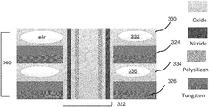
- a memory device 300 is depicted subsequent to a tier deposition of layers that may form a plurality of wordlines, comprising at least in part a memory array in a die 301 . More specifically, the memory device 300 is depicted subsequent to a deposition of polysilicon layers 302 , 304 with respective disposable layers 306 , 308 (e.g., comprising nitride or other suitable material) between the polysilicon layers to ensure structural integrity of the memory device.
- the disposable layers may be replaced by a gate material later in the process.
- the layers 302 , 304 , 306 , and 308 form a layer structure 340 , comprising alternating polysilicon and nitride layers.
- FIG. 3 Only four layers of the structure 340 are depicted in FIG. 3 (and subsequent figures) for ease of understanding. It will be understood that multiple layers (e.g., up to 96) may be provided in the memory device 300 , in a formation depicted in FIGS. 3-9 (and 10 - 14 ).
- the memory device 300 is depicted subsequent to etching pillar holes to form pillars (e.g., space 310 ) in the layered structure of FIG. 3 .
- the pillar etching may be provided through a dry etch process, for example.
- the memory device 300 is depicted subsequent to memory cell stack 322 formation in the space 310 . More specifically, materials consisting of oxide, nitride and polysilicon are deposited to create the top oxide, storage node, tunnel oxide, and channel of memory cells inside. Such formation may be provided, e.g., by the process of atomic layer deposition (ALD). As shown, the memory cell stack 322 includes layers of semi-conductive material 312 (e.g., polysilicon), coupled with dielectric layers 314 , 316 (e.g., oxide, such as SiO2), as shown. The dielectric layer 316 is the tunneling oxide through which electronic charge is transferred between the channel (layer 312 ) and the storage layer 320 during a write and erase operation.
- semi-conductive material 312 e.g., polysilicon
- dielectric layers 314 , 316 e.g., oxide, such as SiO2
- Layer 320 (e.g., nitride, or a combination of oxide and nitride) may be the charge storage layer where programming charge is trapped or de-trapped for programming or erasing of the memory cell.
- Layer 318 is the blocking layer between the storage layer 320 and the control gates ( 324 , 326 ) and may include oxide or other high k dielectrics (e.g., HfOx) or a combination of them.
- the memory device 300 is depicted subsequent to removal of the disposable layers 308 , 306 from the structure 340 . Such removal may be performed to provide a replacement gate for the memory cell stack 322 .
- the memory device 300 is depicted subsequent to a deposition of material to form wordlines to the structure 340 .
- the wordlines include respective gates to control respective memory cells of the memory cell stack 322 , coupled with the wordlines. More specifically, the material forming control gates 324 , 326 may be deposited between respective polysilicon layers 302 , 304 to fill the gaps left after removal of layers 306 , 308 , and to create the gates of the NAND memory array.
- the material comprises a metal, such as tungsten (W) or any other suitable material.
- the gates may comprise a metal.
- the memory device 300 is depicted subsequent to removal of polysilicon layers 302 , 304 from the structure 340 .
- the removal may be performed, e.g., by chemical etching.
- the memory device 300 is depicted subsequent to providing dielectric layers with components configured to reduce capacitance of the structure 340 . More specifically, dielectric layers 330 , 334 are provided to fill the gaps left by the removal of the polysilicon layers 302 , 304 from the structure 340 .
- the dielectric layers 330 , 334 may be provided by the process of airgap isolation fill, for example. As shown, the dielectric layers 330 , 334 include respective components 332 , 336 . In some embodiments, the components 332 , 336 may comprise air gaps inside the layers 330 , 334 .
- dielectric layers 330 , 334 may be deposited with process conditions that may not fully fill the gaps, and may leave air gaps 332 , 336 .
- the components 332 , 336 may comprise dielectric materials with a low dielectric constant, e.g., low-k dielectric material.
- layers 330 , 334 with respective components 332 , 336 may comprise composites of dielectric materials with different dielectric constants, in order to reduce capacitance of the memory device.
- one of the dielectric constants of the dielectric material comprising the composite can be lower than the other one.
- the dielectric constant of the component 332 may be lower than that of the respective layer 330 .
- dielectric layers 330 , 334 may have low-k values. In other words, dielectric layers 330 , 334 may comprise components 332 , 336 and have low-k dielectric material.
- FIGS. 10-14 describe another example process of forming a memory device with reduced capacitance, in accordance with some embodiments. More specifically, FIGS. 10-14 illustrate the process of forming a memory array with polysilicon gates, with reduced capacitance, in accordance with some embodiments.
- a memory device 1000 is depicted subsequent to a tier deposition of layers that may form a plurality of wordlines, comprising at least in part a memory array in a die 1001 . More specifically, the memory device 1000 is depicted subsequent to a deposition of polysilicon layers 1002 , 1004 with respective disposable layers 1006 , 1008 (e.g., comprising nitride or other suitable material) between the polysilicon layers, to form a layered structure 1040 , similar to the process described in reference to FIG. 3 .
- respective disposable layers 1006 , 1008 e.g., comprising nitride or other suitable material
- the memory device 1000 is depicted subsequent to etching spaces to form pillars (e.g., space 1010 ) inside the layered structure 1040 of FIG. 10 , similar to the process described in reference to FIG. 4 .
- FIG. 12 the memory device 1000 is depicted subsequent to memory cell stack 1022 formation, similar to the process described in reference to FIG. 5 .
- the memory device 1000 is depicted subsequent to removal of the disposable layers 1006 , 1008 from the structure 1040 , similar to the process described in reference to FIG. 6 .
- the resulting structure comprises multiple polysilicon layers 1002 , 1004 , to form polysilicon gates to electronically control the memory cells of the memory cell stack 1022 .
- the memory device 1000 is depicted subsequent to providing dielectric layers with components configured to reduce capacitance of the structure 1040 , similar to the process described in reference to FIG. 9 .
- dielectric layers 1030 , 1034 are provided to fill the gaps left by the removal of the disposable layers 1006 , 1008 from the structure 1040 .
- the dielectric layers 1030 , 1034 include respective components 1032 , 1036 .
- the components 1032 , 1036 may comprise air gaps inside the layers 1030 , 1034 .
- the components 1032 , 1036 may comprise dielectric materials with a low dielectric constant, e.g., low-k dielectric material.
- a capping layer may be deposited on top of the memory array.
- the capping layer may include a silicon nitride (SiN), deposited by chemical vapor deposition (CVD), e.g., about 20-30 nm thick.
- the thickness of the capping layer may be based on chemical mechanical polishing/planarization (CMP) for the ability to polish the memory array with sufficient over/under polish margin.
- CMP chemical mechanical polishing/planarization
- the capping layer may be any low temperature film (e.g., below 320 C), including, but not limited to, oxide, polymer, titanium nitride (TiN), or the like.
- FIG. 15 is a process flow diagram for providing a memory device with reduced capacitance, in accordance with some embodiments.
- the process 1500 may comport with actions described in connection with FIGS. 3-14 in some embodiments.
- the process 1500 may apply to formation of wordlines or bitlines in a memory array in accordance with embodiments described herein.
- the application of the process 1500 to formation of wordlines is provided for purposes of illustration and for ease of understanding.
- the process 1500 includes providing one or more pillars in a die that comprises multiple layers, including forming one or more memory cells in a stacked fashion, to form the pillars of a memory array.
- the process 1500 further includes forming a plurality of wordlines of the memory array, to couple with respective pillars comprising memory cell stacks.
- Forming a plurality of wordlines may include various processes, such as dry etch, cleaning, deposition of a liner, and provision of a disposable layer for structural integrity purposes.
- Forming the wordlines further includes depositing dielectric layers between adjacent wordlines of the plurality of wordlines.
- the dielectric layers include a component provided inside the dielectric layer, to reduce capacitance of the wordlines of the memory array.
- such component may include an air gap or a low-k dielectric material disposed inside the dielectric layer.
- the wordlines may include a gate to control memory cells coupled with the wordlines.
- the gates may comprise a metal or a silicon-based material, such as polysilicon.
- the described embodiments provide a number of advantages compared to conventional solutions. For example, replacing continuous dielectric layers between wordlines of a memory array with partial dielectric layers, e.g., dielectric layers having an air gap inside them or low-k material disposed inside them, may reduce the overall wordline capacitance. This may improve the memory device performance by reducing the time required to operate the memory device.
- partial dielectric layers e.g., dielectric layers having an air gap inside them or low-k material disposed inside them
- the described embodiments may be implemented in a three-dimensional memory array, such as a 3D NAND memory array.
- the partial dielectric layers between the wordlines provided according to the embodiments described herein may be implemented in a two-dimensional memory array, such as a 2D NAND memory array.
- the memory arrays and methods described herein may be implemented into a system using any suitable hardware and/or software to configure as desired.
- FIG. 16 schematically illustrates an example computing device including a memory device with reduced capacitance, in accordance with some embodiments.
- the computing device 1600 includes system control logic 1608 coupled to one or more processor(s) 1604 ; a memory device 1612 having a memory device 300 ( 1000 ) described in reference to FIGS. 3-15 ; one or more communications interface(s) 1616 ; and input/output (I/O) devices 1620 .
- system control logic 1608 coupled to one or more processor(s) 1604 ; a memory device 1612 having a memory device 300 ( 1000 ) described in reference to FIGS. 3-15 ; one or more communications interface(s) 1616 ; and input/output (I/O) devices 1620 .
- the memory device 1612 may be a non-volatile computer storage chip (e.g., provided on the die 102 of FIGS. 1-2 ) that may include the memory device 300 ( 1000 ) of FIGS. 3-15 .
- the memory device 1612 comprises a package, such as IC assembly 200 of FIG. 2 , having the memory device 300 (or 1000 ) disposed therein, driver circuitry (e.g., drivers), input/output connections to electrically couple the memory device 1612 with other components of the computing device 1600 , etc.
- the memory device 1612 may be configured to be removably or permanently coupled with the computing device 1600 .
- Communications interface(s) 1616 may provide an interface for computing device 1600 to communicate over one or more network(s) and/or with any other suitable device.
- Communications interface(s) 1616 may include any suitable hardware and/or firmware.
- Communications interface(s) 1616 for one embodiment may include, for example, a network adapter, a wireless network adapter, a telephone modem, and/or a wireless modem.
- communications interface(s) 1616 for one embodiment may use one or more antennas to communicatively couple the computing device 1600 with a wireless network.
- At least one of the processor(s) 1604 may be packaged together with logic for one or more controller(s) of system control logic 1608 .
- at least one of the processor(s) 1604 may be packaged together with logic for one or more controllers of system control logic 1608 to form a System in Package (SiP).
- SiP System in Package
- at least one of the processor(s) 1604 may be integrated on the same die with logic for one or more controller(s) of system control logic 1608 .
- at least one of the processor(s) 1604 may be integrated on the same die with logic for one or more controller(s) of system control logic 1608 to form a System on Chip (SoC).
- SoC System on Chip
- System control logic 1608 may include any suitable interface controllers to provide for any suitable interface to at least one of the processor(s) 1604 and/or to any suitable device or component in communication with system control logic 1608 .
- the system control logic 1608 may move data into and/or out of the various components of the computing device 1600 .
- System control logic 1608 for one embodiment may include a memory controller 1624 to provide an interface to the memory device 1612 to control various memory access operations.
- the memory controller 1624 may include control logic 1628 that may be specifically configured to control access of the memory device 1612 .
- the I/O devices 1620 may include user interfaces designed to enable user interaction with the computing device 1600 , peripheral component interfaces designed to enable peripheral component interaction with the computing device 1600 , and/or sensors designed to determine environmental conditions and/or location information related to the computing device 1600 .
- the user interfaces could include, but are not limited to, a display, e.g., a liquid crystal display, a touch screen display, etc., a speaker, a microphone, one or more digital cameras to capture pictures and/or video, a flashlight (e.g., a light emitting diode flash), and a keyboard.
- the peripheral component interfaces may include, but are not limited to, a non-volatile memory port, an audio jack, and a power supply interface.
- the sensors may include, but are not limited to, a gyro sensor, an accelerometer, a proximity sensor, an ambient light sensor, and a positioning unit.
- the positioning unit may additionally/alternatively be part of, or interact with, the communication interface(s) 1616 to communicate with components of a positioning network, e.g., a global positioning system (GPS) satellite.
- GPS global positioning system
- the computing device 1600 may be a mobile computing device such as, but not limited to, a laptop computing device, a tablet computing device, a netbook, a smartphone, etc.; a desktop computing device; a workstation; a server; etc.
- the computing device 1600 may have more or fewer components, and/or different architectures.
- the computing device 1600 may be any other electronic device that processes data.
- the present disclosure describes a number of examples.
- Example 1 is an apparatus, comprising: a memory array formed in a die, wherein the memory array includes one or more pillars and a plurality of wordlines coupled with the one or more pillars, wherein adjacent wordlines of the plurality of wordlines are separated by respective dielectric layers, wherein the dielectric layers include respective components provided to reduce capacitance of the plurality of wordlines.
- Example 2 may include the apparatus of Example 1, wherein the components include an air gap provided inside the dielectric layers.
- Example 3 may include the apparatus of Example 1, wherein the components include a low-k dielectric material.
- Example 4 may include the apparatus of Example 1, wherein each of the one or more pillars comprise one or more memory cells formed in a stacked fashion.
- Example 5 may include the apparatus of Example 1, wherein a wordline of the plurality of wordlines includes a gate to control a memory cell coupled with the wordline, wherein the gate comprises one of: a metal or a silicon-based material.
- Example 6 may include the apparatus of Example 5, wherein the metal comprises tungsten (W).
- Example 7 may include the apparatus of Example 5, wherein the silicon-based material comprises polysilicon.
- Example 8 may include the apparatus of Example 1, wherein the memory array comprises a three-dimensional (3D) NAND memory array.
- Example 9 may include any of the apparatuses of Examples 1-8, wherein the apparatus comprises an integrated circuit.
- Example 10 is a computing system, comprising: a processor; and a memory coupled with the processor, wherein the memory includes a memory array formed in a die, wherein the memory array includes one or more pillars and a plurality of wordlines coupled with the one or more pillars, wherein adjacent wordlines of the plurality of wordlines are separated by respective dielectric layers, wherein the dielectric layers include respective components provided to reduce capacitance of the plurality of wordlines.
- Example 11 may include the computing system of Example 10, wherein the components include an air gap provided inside the dielectric layers.
- Example 12 may include the computing system of Example 10, wherein the components include a low-k dielectric material.
- Example 13 may include the computing system of Example 10, wherein each of the one or more pillars comprise one or more memory cells formed in a stacked fashion.
- Example 14 may include the computing system of Example 10, wherein a wordline of the plurality of wordlines includes a gate to control a memory cell coupled with the wordline, wherein the gate comprises one of: a metal or a silicon-based material.
- Example 15 may include any of the computing systems of Examples 10 to 14, wherein the computing system is a mobile computing device.
- Example 16 is a method, comprising: forming one or more pillars comprising memory cells in a die, to form a memory array; and providing a plurality of wordlines to couple with respective ones of the one or more pillars, including separating adjacent wordlines of the plurality of wordlines by respective dielectric layers, and forming respective components in the dielectric layers, to reduce capacitance of the plurality of wordlines.
- Example 17 may include the method of Example 16, wherein forming the components includes providing an air gap inside the dielectric layers.
- Example 18 may include the method of Example 16, wherein forming the components includes providing the dielectric layers with low-k dielectric material.
- Example 19 may include the method of Example 16, wherein providing the plurality of wordlines includes, for a wordline, forming a gate to control a memory cell coupled with the wordline, wherein the gate comprises one of: a metal or a silicon-based material.
- Example 20 may include any of the methods of Examples 16 to 19, wherein the memory array comprises a three-dimensional (3D) NAND memory array.
- Various embodiments may include any suitable combination of the above-described embodiments including alternative (or) embodiments of embodiments that are described in conjunctive form (and) above (e.g., the “and” may be “and/or”). Furthermore, some embodiments may include one or more articles of manufacture (e.g., non-transitory computer-readable media) having instructions, stored thereon, that when executed result in actions of any of the above-described embodiments. Moreover, some embodiments may include apparatuses or systems having any suitable means for carrying out the various operations of the above-described embodiments.
Landscapes
- Physics & Mathematics (AREA)
- Geometry (AREA)
- Semiconductor Memories (AREA)
- Non-Volatile Memory (AREA)
Abstract
Description
Claims (14)
Priority Applications (1)
| Application Number | Priority Date | Filing Date | Title |
|---|---|---|---|
| US16/021,550 US10861867B2 (en) | 2018-06-28 | 2018-06-28 | Memory device with reduced capacitance |
Applications Claiming Priority (1)
| Application Number | Priority Date | Filing Date | Title |
|---|---|---|---|
| US16/021,550 US10861867B2 (en) | 2018-06-28 | 2018-06-28 | Memory device with reduced capacitance |
Publications (2)
| Publication Number | Publication Date |
|---|---|
| US20190043882A1 US20190043882A1 (en) | 2019-02-07 |
| US10861867B2 true US10861867B2 (en) | 2020-12-08 |
Family
ID=65230429
Family Applications (1)
| Application Number | Title | Priority Date | Filing Date |
|---|---|---|---|
| US16/021,550 Active US10861867B2 (en) | 2018-06-28 | 2018-06-28 | Memory device with reduced capacitance |
Country Status (1)
| Country | Link |
|---|---|
| US (1) | US10861867B2 (en) |
Families Citing this family (4)
| Publication number | Priority date | Publication date | Assignee | Title |
|---|---|---|---|---|
| US11211378B2 (en) | 2019-07-18 | 2021-12-28 | International Business Machines Corporation | Heterogeneous integration structure for artificial intelligence computing |
| KR102683913B1 (en) | 2019-09-03 | 2024-07-11 | 삼성전자주식회사 | Vertical memory devices and methods of manufacturing the same |
| US12156411B2 (en) * | 2022-04-13 | 2024-11-26 | Micron Technology, Inc. | Memory array having air gaps |
| KR20240150062A (en) * | 2023-04-07 | 2024-10-15 | 에스케이하이닉스 주식회사 | Semiconductor dedvice and method for fabricating the same |
Citations (7)
| Publication number | Priority date | Publication date | Assignee | Title |
|---|---|---|---|---|
| US20130148398A1 (en) * | 2011-12-13 | 2013-06-13 | SK Hynix Inc. | Three-dimensional non-volatile memory device, memory system including the same and method of manufacturing the same |
| US20160118396A1 (en) * | 2014-10-22 | 2016-04-28 | SanDisk Technologies, Inc. | Three dimensional nand device containing fluorine doped layer and method of making thereof |
| US20160268293A1 (en) * | 2015-03-09 | 2016-09-15 | Kabushiki Kaisha Toshiba | Semiconductor device |
| US20170062330A1 (en) * | 2015-08-28 | 2017-03-02 | Jeeyong Kim | Three-dimensional semiconductor memory device |
| US20180108664A1 (en) * | 2016-10-14 | 2018-04-19 | Jeong Gil Lee | Memory Devices Using Etching Stop Layers |
| US20180269181A1 (en) * | 2017-03-14 | 2018-09-20 | STATS ChipPAC Pte. Ltd. | System -in-Package with Double-Sided Molding |
| US10141221B1 (en) * | 2017-07-18 | 2018-11-27 | Macronix International Co., Ltd. | Method for manufacturing three dimensional stacked semiconductor structure and structure manufactured by the same |
-
2018
- 2018-06-28 US US16/021,550 patent/US10861867B2/en active Active
Patent Citations (8)
| Publication number | Priority date | Publication date | Assignee | Title |
|---|---|---|---|---|
| US20130148398A1 (en) * | 2011-12-13 | 2013-06-13 | SK Hynix Inc. | Three-dimensional non-volatile memory device, memory system including the same and method of manufacturing the same |
| US20160118396A1 (en) * | 2014-10-22 | 2016-04-28 | SanDisk Technologies, Inc. | Three dimensional nand device containing fluorine doped layer and method of making thereof |
| US20160268293A1 (en) * | 2015-03-09 | 2016-09-15 | Kabushiki Kaisha Toshiba | Semiconductor device |
| US20170062330A1 (en) * | 2015-08-28 | 2017-03-02 | Jeeyong Kim | Three-dimensional semiconductor memory device |
| US9666525B2 (en) * | 2015-08-28 | 2017-05-30 | Samsung Electronics Co., Ltd. | Three-dimensional semiconductor memory device |
| US20180108664A1 (en) * | 2016-10-14 | 2018-04-19 | Jeong Gil Lee | Memory Devices Using Etching Stop Layers |
| US20180269181A1 (en) * | 2017-03-14 | 2018-09-20 | STATS ChipPAC Pte. Ltd. | System -in-Package with Double-Sided Molding |
| US10141221B1 (en) * | 2017-07-18 | 2018-11-27 | Macronix International Co., Ltd. | Method for manufacturing three dimensional stacked semiconductor structure and structure manufactured by the same |
Also Published As
| Publication number | Publication date |
|---|---|
| US20190043882A1 (en) | 2019-02-07 |
Similar Documents
| Publication | Publication Date | Title |
|---|---|---|
| US10629652B2 (en) | Dual-layer dielectric in memory device | |
| JP7328344B2 (en) | 3D memory device | |
| US11864367B2 (en) | Bonded semiconductor devices having processor and NAND flash memory and methods for forming the same | |
| EP3891798B1 (en) | Bonded semiconductor devices having processor and nand flash memory and methods for forming the same | |
| JP7197719B2 (en) | Semiconductor device and method | |
| EP3891786B1 (en) | Stacked three-dimensional heterogeneous memory devices and methods for forming same | |
| EP3928353B1 (en) | Three-dimensional memory device with three-dimensional phase-change memory | |
| CN107112345B (en) | Electrode configuration to increase electrical and thermal isolation of phase change memory elements | |
| US10861867B2 (en) | Memory device with reduced capacitance | |
| CN107004693B (en) | Phase change memory cell injection for dummy array leakage reduction | |
| KR102682594B1 (en) | Providing structural integrity in memory devices | |
| US10607695B2 (en) | Provision of structural integrity in memory device | |
| US20260020257A1 (en) | Three-dimensional semiconductor devices and manufacturing methods thereof |
Legal Events
| Date | Code | Title | Description |
|---|---|---|---|
| FEPP | Fee payment procedure |
Free format text: ENTITY STATUS SET TO UNDISCOUNTED (ORIGINAL EVENT CODE: BIG.); ENTITY STATUS OF PATENT OWNER: LARGE ENTITY |
|
| AS | Assignment |
Owner name: INTEL CORPORATION, CALIFORNIA Free format text: ASSIGNMENT OF ASSIGNORS INTEREST;ASSIGNORS:HASNAT, KHALED;MAJHI, PRASHANT;PARAT, KRISHNA;SIGNING DATES FROM 20180615 TO 20180708;REEL/FRAME:046489/0511 |
|
| STPP | Information on status: patent application and granting procedure in general |
Free format text: DOCKETED NEW CASE - READY FOR EXAMINATION |
|
| STPP | Information on status: patent application and granting procedure in general |
Free format text: NON FINAL ACTION MAILED |
|
| STPP | Information on status: patent application and granting procedure in general |
Free format text: RESPONSE TO NON-FINAL OFFICE ACTION ENTERED AND FORWARDED TO EXAMINER |
|
| STPP | Information on status: patent application and granting procedure in general |
Free format text: FINAL REJECTION MAILED |
|
| STPP | Information on status: patent application and granting procedure in general |
Free format text: RESPONSE AFTER FINAL ACTION FORWARDED TO EXAMINER |
|
| STPP | Information on status: patent application and granting procedure in general |
Free format text: ADVISORY ACTION MAILED |
|
| STPP | Information on status: patent application and granting procedure in general |
Free format text: DOCKETED NEW CASE - READY FOR EXAMINATION |
|
| STPP | Information on status: patent application and granting procedure in general |
Free format text: RESPONSE TO NON-FINAL OFFICE ACTION ENTERED AND FORWARDED TO EXAMINER |
|
| STPP | Information on status: patent application and granting procedure in general |
Free format text: NOTICE OF ALLOWANCE MAILED -- APPLICATION RECEIVED IN OFFICE OF PUBLICATIONS |
|
| STPP | Information on status: patent application and granting procedure in general |
Free format text: PUBLICATIONS -- ISSUE FEE PAYMENT VERIFIED |
|
| STCF | Information on status: patent grant |
Free format text: PATENTED CASE |
|
| AS | Assignment |
Owner name: INTEL NDTM US LLC, CALIFORNIA Free format text: ASSIGNMENT OF ASSIGNORS INTEREST;ASSIGNOR:INTEL CORPORATION;REEL/FRAME:064928/0832 Effective date: 20211229 |
|
| MAFP | Maintenance fee payment |
Free format text: PAYMENT OF MAINTENANCE FEE, 4TH YEAR, LARGE ENTITY (ORIGINAL EVENT CODE: M1551); ENTITY STATUS OF PATENT OWNER: LARGE ENTITY Year of fee payment: 4 |