US10859407B2 - Motion sensing using hall voltage signals - Google Patents
Motion sensing using hall voltage signals Download PDFInfo
- Publication number
- US10859407B2 US10859407B2 US16/581,661 US201916581661A US10859407B2 US 10859407 B2 US10859407 B2 US 10859407B2 US 201916581661 A US201916581661 A US 201916581661A US 10859407 B2 US10859407 B2 US 10859407B2
- Authority
- US
- United States
- Prior art keywords
- magnetic field
- coil
- mass
- location
- along
- Prior art date
- Legal status (The legal status is an assumption and is not a legal conclusion. Google has not performed a legal analysis and makes no representation as to the accuracy of the status listed.)
- Expired - Fee Related
Links
- 230000033001 locomotion Effects 0.000 title claims description 35
- 230000005355 Hall effect Effects 0.000 claims abstract description 46
- 239000000758 substrate Substances 0.000 claims abstract description 27
- 238000006073 displacement reaction Methods 0.000 claims description 134
- 238000005259 measurement Methods 0.000 claims description 47
- 238000000034 method Methods 0.000 claims description 41
- 239000011159 matrix material Substances 0.000 claims description 28
- 230000004044 response Effects 0.000 claims description 8
- 230000008859 change Effects 0.000 description 46
- 238000000926 separation method Methods 0.000 description 35
- 238000012545 processing Methods 0.000 description 28
- 230000008569 process Effects 0.000 description 25
- 238000005516 engineering process Methods 0.000 description 20
- 230000035945 sensitivity Effects 0.000 description 13
- 239000003550 marker Substances 0.000 description 12
- 230000008878 coupling Effects 0.000 description 9
- 238000010168 coupling process Methods 0.000 description 9
- 238000005859 coupling reaction Methods 0.000 description 9
- 238000006243 chemical reaction Methods 0.000 description 7
- 230000004907 flux Effects 0.000 description 6
- 229910001220 stainless steel Inorganic materials 0.000 description 6
- 239000010935 stainless steel Substances 0.000 description 6
- 230000008901 benefit Effects 0.000 description 5
- 230000003750 conditioning effect Effects 0.000 description 5
- 230000000737 periodic effect Effects 0.000 description 3
- 238000012546 transfer Methods 0.000 description 3
- 238000004804 winding Methods 0.000 description 3
- XUIMIQQOPSSXEZ-UHFFFAOYSA-N Silicon Chemical compound [Si] XUIMIQQOPSSXEZ-UHFFFAOYSA-N 0.000 description 2
- 238000010586 diagram Methods 0.000 description 2
- 230000006872 improvement Effects 0.000 description 2
- 238000005070 sampling Methods 0.000 description 2
- 239000004065 semiconductor Substances 0.000 description 2
- 229910052710 silicon Inorganic materials 0.000 description 2
- 239000010703 silicon Substances 0.000 description 2
- 238000004088 simulation Methods 0.000 description 2
- 238000012795 verification Methods 0.000 description 2
- 238000012935 Averaging Methods 0.000 description 1
- RYGMFSIKBFXOCR-UHFFFAOYSA-N Copper Chemical compound [Cu] RYGMFSIKBFXOCR-UHFFFAOYSA-N 0.000 description 1
- 238000006842 Henry reaction Methods 0.000 description 1
- 206010048643 Hypereosinophilic syndrome Diseases 0.000 description 1
- 230000001133 acceleration Effects 0.000 description 1
- 230000009471 action Effects 0.000 description 1
- 230000003213 activating effect Effects 0.000 description 1
- 238000013459 approach Methods 0.000 description 1
- 238000003491 array Methods 0.000 description 1
- 230000005540 biological transmission Effects 0.000 description 1
- 238000004364 calculation method Methods 0.000 description 1
- 239000003990 capacitor Substances 0.000 description 1
- 238000004891 communication Methods 0.000 description 1
- 229910052802 copper Inorganic materials 0.000 description 1
- 239000010949 copper Substances 0.000 description 1
- 238000012937 correction Methods 0.000 description 1
- 238000013461 design Methods 0.000 description 1
- 230000005669 field effect Effects 0.000 description 1
- 230000010354 integration Effects 0.000 description 1
- 238000001459 lithography Methods 0.000 description 1
- 238000004519 manufacturing process Methods 0.000 description 1
- 238000013507 mapping Methods 0.000 description 1
- 238000000691 measurement method Methods 0.000 description 1
- 238000012986 modification Methods 0.000 description 1
- 230000004048 modification Effects 0.000 description 1
- 230000003071 parasitic effect Effects 0.000 description 1
- 229910021420 polycrystalline silicon Inorganic materials 0.000 description 1
- 238000013139 quantization Methods 0.000 description 1
- 230000008707 rearrangement Effects 0.000 description 1
- 238000009877 rendering Methods 0.000 description 1
- 230000003068 static effect Effects 0.000 description 1
- 238000010408 sweeping Methods 0.000 description 1
- 238000012360 testing method Methods 0.000 description 1
Images


Classifications
-
- G—PHYSICS
- G01—MEASURING; TESTING
- G01D—MEASURING NOT SPECIALLY ADAPTED FOR A SPECIFIC VARIABLE; ARRANGEMENTS FOR MEASURING TWO OR MORE VARIABLES NOT COVERED IN A SINGLE OTHER SUBCLASS; TARIFF METERING APPARATUS; MEASURING OR TESTING NOT OTHERWISE PROVIDED FOR
- G01D5/00—Mechanical means for transferring the output of a sensing member; Means for converting the output of a sensing member to another variable where the form or nature of the sensing member does not constrain the means for converting; Transducers not specially adapted for a specific variable
- G01D5/12—Mechanical means for transferring the output of a sensing member; Means for converting the output of a sensing member to another variable where the form or nature of the sensing member does not constrain the means for converting; Transducers not specially adapted for a specific variable using electric or magnetic means
- G01D5/14—Mechanical means for transferring the output of a sensing member; Means for converting the output of a sensing member to another variable where the form or nature of the sensing member does not constrain the means for converting; Transducers not specially adapted for a specific variable using electric or magnetic means influencing the magnitude of a current or voltage
- G01D5/20—Mechanical means for transferring the output of a sensing member; Means for converting the output of a sensing member to another variable where the form or nature of the sensing member does not constrain the means for converting; Transducers not specially adapted for a specific variable using electric or magnetic means influencing the magnitude of a current or voltage by varying inductance, e.g. by a movable armature
- G01D5/2006—Mechanical means for transferring the output of a sensing member; Means for converting the output of a sensing member to another variable where the form or nature of the sensing member does not constrain the means for converting; Transducers not specially adapted for a specific variable using electric or magnetic means influencing the magnitude of a current or voltage by varying inductance, e.g. by a movable armature by influencing the self-induction of one or more coils
- G01D5/2013—Mechanical means for transferring the output of a sensing member; Means for converting the output of a sensing member to another variable where the form or nature of the sensing member does not constrain the means for converting; Transducers not specially adapted for a specific variable using electric or magnetic means influencing the magnitude of a current or voltage by varying inductance, e.g. by a movable armature by influencing the self-induction of one or more coils by a movable ferromagnetic element, e.g. a core
-
- G—PHYSICS
- G01—MEASURING; TESTING
- G01D—MEASURING NOT SPECIALLY ADAPTED FOR A SPECIFIC VARIABLE; ARRANGEMENTS FOR MEASURING TWO OR MORE VARIABLES NOT COVERED IN A SINGLE OTHER SUBCLASS; TARIFF METERING APPARATUS; MEASURING OR TESTING NOT OTHERWISE PROVIDED FOR
- G01D5/00—Mechanical means for transferring the output of a sensing member; Means for converting the output of a sensing member to another variable where the form or nature of the sensing member does not constrain the means for converting; Transducers not specially adapted for a specific variable
- G01D5/12—Mechanical means for transferring the output of a sensing member; Means for converting the output of a sensing member to another variable where the form or nature of the sensing member does not constrain the means for converting; Transducers not specially adapted for a specific variable using electric or magnetic means
- G01D5/14—Mechanical means for transferring the output of a sensing member; Means for converting the output of a sensing member to another variable where the form or nature of the sensing member does not constrain the means for converting; Transducers not specially adapted for a specific variable using electric or magnetic means influencing the magnitude of a current or voltage
- G01D5/142—Mechanical means for transferring the output of a sensing member; Means for converting the output of a sensing member to another variable where the form or nature of the sensing member does not constrain the means for converting; Transducers not specially adapted for a specific variable using electric or magnetic means influencing the magnitude of a current or voltage using Hall-effect devices
- G01D5/145—Mechanical means for transferring the output of a sensing member; Means for converting the output of a sensing member to another variable where the form or nature of the sensing member does not constrain the means for converting; Transducers not specially adapted for a specific variable using electric or magnetic means influencing the magnitude of a current or voltage using Hall-effect devices influenced by the relative movement between the Hall device and magnetic fields
-
- G—PHYSICS
- G01—MEASURING; TESTING
- G01D—MEASURING NOT SPECIALLY ADAPTED FOR A SPECIFIC VARIABLE; ARRANGEMENTS FOR MEASURING TWO OR MORE VARIABLES NOT COVERED IN A SINGLE OTHER SUBCLASS; TARIFF METERING APPARATUS; MEASURING OR TESTING NOT OTHERWISE PROVIDED FOR
- G01D5/00—Mechanical means for transferring the output of a sensing member; Means for converting the output of a sensing member to another variable where the form or nature of the sensing member does not constrain the means for converting; Transducers not specially adapted for a specific variable
- G01D5/12—Mechanical means for transferring the output of a sensing member; Means for converting the output of a sensing member to another variable where the form or nature of the sensing member does not constrain the means for converting; Transducers not specially adapted for a specific variable using electric or magnetic means
- G01D5/14—Mechanical means for transferring the output of a sensing member; Means for converting the output of a sensing member to another variable where the form or nature of the sensing member does not constrain the means for converting; Transducers not specially adapted for a specific variable using electric or magnetic means influencing the magnitude of a current or voltage
- G01D5/142—Mechanical means for transferring the output of a sensing member; Means for converting the output of a sensing member to another variable where the form or nature of the sensing member does not constrain the means for converting; Transducers not specially adapted for a specific variable using electric or magnetic means influencing the magnitude of a current or voltage using Hall-effect devices
Definitions
- the present disclosure is generally related to motion sensing.
- aspects of the present disclosure are related to localizing a moving magnet using an array of asymmetrically distributed Hall-effect sensing elements.
- aspects of the present disclosure are related to localizing a moving magnet based on Hall voltage signals and back electromotive force (bEMF) signals that are concurrently acquired using a hybrid sensor that includes a Hall effect sensor (HES) and a sensing coil.
- bEMF back electromotive force
- a haptic engine (also referred to as a vibration module) is a linear resonant actuator that determines one of acceleration, velocity and displacement of a moving mass.
- FIGS. 12A-12B show aspects of a conventional haptic engine (HE) in which position of a magnet (M), that is moving relative to a fixed coil (C), is encoded in the intensity of magnetic field flux and sensed by Hall-effect sensing elements (HSEs), also referred to interchangeably as HESs or simply Hall sensors, disposed on a top side of the coil, and on a bottom side of the coil.
- HESs Hall-effect sensing elements
- a displacement ⁇ X along the x-axis and a displacement ⁇ Z along the z-axis of the magnet, that is moving relative to the fixed coil is determined as:
- LUT is a look-up table mapping the measured value of the field caused only by the magnet and a corresponding value of the displacement.
- FIG. 12C shows examples of errors of the displacement measurements for various frequencies of driving currents.
- a sensing error can be caused by the inaccuracy of ⁇ .
- a conventional HE needs an external reference displacement sensor (e.g., laser or bEMF model fitting, etc.) for calibration, as shown in FIG. 12C .
- an external reference displacement sensor e.g., laser or bEMF model fitting, etc.
- bEMF can be determined conventionally using the driving coil itself, in the following manner:
- bEMF V - RI - L ⁇ dI dt - R ⁇ ⁇ ⁇ ADC ⁇ dI dt , ( 4 )
- R and L are the resistance and inductance, respectively, of the driving coil.
- the first term is the voltage across the driving coil
- the second term is a driver term
- the third term is an inductance term.
- accuracy of bEMF-based motion sensing is prone to a number of error sources.
- the coil resistance R is very sensitive to temperature changes and quantization error associated with analog-to-digital conversion (ADC).
- ADC analog-to-digital conversion
- copper's temperature coefficient of resistance is approximately 0.4%/deg C.
- Eq. (4) Another error source in Eq. (4) is the timing synchronization between driving coil voltage V and driving coil current I when an ADC delay ⁇ ADC between the measured driving coil voltage V and measured driving coil current I is finite (i.e., non-zero).
- a finite false inductance term given by the fourth term in EQ. (4), can be sensed as part of bEMF, as shown in FIG. 12C .
- Such timing synchronization can be expressed as
- ⁇ D is the group delay between voltage and current caused by the inductance
- L E is the false inductance term caused by the ADC group delay
- technologies are described for measuring displacements of a moving mass, which is part of a magnetic field source, by using an array of asymmetrically distributed magnetic field sensing elements.
- Other technologies described in this disclosure are directed to localizing a moving magnet based on Hall voltage signals and bEMF signals concurrently acquired using a hybrid sensor that includes a HES and a sensing coil.
- the magnetic field sensing elements can be Hall-effect sensing elements fabricated, using CMOS technologies, as part of an integrated circuit chip.
- the array of asymmetrically distributed Hall-effect sensing elements or the hybrid sensor along with driving circuitry, conditioning circuitry and processing circuitry can be integrated in an application specific integrated circuit (ASIC).
- ASIC application specific integrated circuit
- One aspect of the disclosure can be implemented as an integrated circuit (IC) chip that includes a first magnetic field sensing element disposed at a first location of the IC chip; a second magnetic field sensing element disposed at a second location of the IC chip; and a third magnetic field sensing element disposed at a third location of the IC chip, the first location, the second location and the third location being distributed along a first direction, such that the second location is between the first location and the third location, and the second location is separated from the first location by a first distance and from the third location by a second distance different from the first distance; and signal processing circuit configured to determine displacements of a mass, when the mass is in motion along a direction of motion having a first component along the first direction and a second component along a second direction normal to the IC chip, where the mass supports at least a portion of a magnetic field source, and where the displacements of the mass are determined, at least in part, based on location-specific changes of a magnetic field emitted by the magnetic field source, the magnetic
- Implementations can include one or more of the following features.
- the location specific magnetic field changes can include magnetic field changes sensed at the first location by the first magnetic field sensing element, magnetic field changes sensed at the second location by the second magnetic field sensing element, and magnetic field changes sensed at the third location by the third magnetic field sensing element.
- the signal processing circuit can be disposed in an area of the IC chip that is between the second location and third location along the first direction, and the second distance is larger than the first distance.
- the determined displacements of the mass can include a displacement ⁇ X along the first direction (e.g., the x-axis) and a displacement ⁇ Z along the second direction (e.g., the z-axis).
- each of the first, second and third magnetic field sensing elements can be configured to sense a component of the magnetic field along the second direction.
- each of the first, second and third magnetic field sensing elements can include a uniaxial Hall-effect sensor element.
- each of the first, second and third magnetic field sensing elements is configured to (i) sense components of the magnetic field along each of the first direction, the second direction and a third direction orthogonal on both the first direction and the second direction, and (ii) provide to the signal processing circuit an angle of the magnetic field relative to the second direction and a magnitude of the magnetic field.
- each of the first, second and third magnetic field sensing elements can include a tri-axial Hall-effect sensor element.
- the IC chip can include a fourth magnetic field sensing element disposed at a fourth location of the IC chip, the fourth location being separated from the first location by a third distance along a third direction orthogonal on both the first direction and the second direction.
- the direction of motion has a third component along the third direction
- the determined displacements of the mass further include a displacement ⁇ Y along the third direction (e.g., the y-axis).
- the IC chip can include a fifth magnetic field sensing element disposed at a fifth location of the IC chip, the fifth location being separated from the third location by the third distance along the third direction and from the fourth location by a sum of the first distance and second distance along the first direction.
- the IC chip can include a sixth magnetic field sensing element disposed at a sixth location of the IC chip, the sixth location being (i) between the fourth location and the fifth location, (ii) separated from the fourth location by the first distance along the first direction, and (iii) separated from the second location by the third distance along the third direction; a seventh magnetic field sensing element disposed at a seventh location of the IC chip, such that the third location is between the second location and the seventh location, where the seventh location is separated from the third location by the first distance along the first direction; and an eighth magnetic field sensing element disposed at an eighth location of the IC chip such that the fifth location is between the sixth location and the seventh eighth, where the eighth location is separated from the fifth location by the first distance along the first direction, and separated from the seventh location by the third distance along the third direction.
- the magnetic field sensing elements provide to the signal processing circuit a gradient along the first direction of the magnetic field, e.g., ⁇ 2 B Z / ⁇ X 2 .
- the IC chip can include one or more driving circuits each of which includes a programmable current source; two or more of the magnetic field sensing elements; and a dummy load connected to each other in series. Additionally, the IC chip can include a band-gap reference circuit; sample and hold circuits; and for each of the driving circuits, (i) a multiplexer circuit including input ports and an output port, where an output of each of the magnetic field sensing elements, the dummies and the band-gap reference circuit is coupled with a respective input port of the multiplexer through a respective sample and hold circuit; (ii) a programmable gain amplifier circuit coupled with the output port of the multiplexer circuit; and (iii) an analog to digital converter (ADC) circuit coupled between the programmable gain amplifier circuit and the signal processing circuit.
- ADC analog to digital converter
- the IC chip can include a chopping multiplexer pair coupled between the output port of the multiplexer circuit and the input of the programmable gain amplifier circuit and between the output of the programmable gain amplifier circuit and the input of the ADC circuit.
- the signal processing circuit and one or more of the dummy loads, the band-gap reference circuit, sample and hold circuits, multiplexer circuits, programmable gain amplifier circuits and ADCs are disposed in a central area of the IC chip that is between the second location and third location along the first direction, and the second distance is larger than the first distance.
- the signal processing circuit can determine, when the mass is at rest, a gradient of the magnetic field along the first direction based on (i) a value of the magnetic field sensed by the first magnetic field sensing element at the first location, (ii) a value of the magnetic field sensed by the second magnetic field sensing element at the second location, and (iii) the first distance between the first location and the second location.
- the displacements of the mass are determined based on a combination of the location-specific changes of the magnetic field and the gradient of the magnetic field along the first direction.
- the signal processing circuit can include a microcontroller unit. In some implementations, the signal processing circuit can include a Field-Programmable Gate Array. In some implementations, the IC chip can be an application specific IC (ASIC).
- ASIC application specific IC
- Another aspect of the disclosure can be implemented as a haptic engine that includes the mass and the above-summarized IC chip.
- Another aspect of the disclosure can be implemented as a computing device that includes the haptic engine.
- Another aspect of the disclosure can be implemented as a displacement measurement system that includes a substrate; a first magnetic field sensing element disposed at a first location of the substrate; a second magnetic field sensing element disposed at a second location of the substrate; and a third magnetic field sensing element disposed at a third location of the substrate, the first location, the second location and the third location being distributed along a first direction, such that the second location is between the first location and the third location, and the second location is separated from the first location by a first distance and from the third location by a second distance larger than the first distance by a predetermined factor; and signal processing circuit configured to determine displacements of a mass, when the mass is in motion along a direction of motion having a first component along the first direction and a second component along a second direction normal to the IC chip, where the mass supports at least a portion of a magnetic field source, and where the displacements of the mass are determined, at least in part, based on location-specific changes of a magnetic field emitted by the magnetic field source,
- Implementations can include one or more of the following features.
- the predetermined factor can be a range of 1.1 to 10.
- the signal processing circuit can be disposed in an area of the substrate that is between the second location and third location along the first direction.
- the substrate, the first magnetic field sensing element, the second magnetic field sensing element, and the third magnetic field sensing element can be included in an integrated circuit chip.
- the substrate is a PCB board; and the first magnetic field sensing element is formed on a first chip, the second magnetic field sensing element is formed on a second chip, and the third magnetic field sensing element is formed on a third chip.
- the array of asymmetrically distributed HSEs can measure ⁇ X, ⁇ Y and ⁇ Z at the same time, can measure rotation around X, Y, and Z axes, and can differentiate rotational motion from translational motion.
- the array of asymmetrically distributed magnetic field sensing elements can be placed closer to the magnetic field source of the haptic engine and away from potential dead-zones, compared to the HSEs used in the conventional haptic engine in FIGS. 12A-12B .
- the array of asymmetrically distributed magnetic field sensing elements can be self-calibrated.
- the array of asymmetrically distributed magnetic field sensing elements is integrated in a single CMOS chip or SoC along with necessary driver circuitry, unlike the HSEs used in the conventional haptic engine in FIGS. 12A-12B that are driven with external circuitry.
- the chip can be disposed, as part of a haptic engine, on a single side of a magnetic field source.
- the HSEs used in the conventional haptic engine in FIGS. 12A-12B are disposed, inside a conventional haptic engine, above and below the magnet, and for this reason, results of the displacement measurements taken with the two conventionally placed HSEs are sensitive to alignment of the HSEs.
- ⁇ Z measurements can be performed with the array of asymmetrically distributed magnetic field sensing elements in a ratiometric manner, in which case results of the ⁇ Z measurements are intrinsically insensitive to temperature change.
- Another aspect of the disclosure can be implemented as an integrated circuit (IC) chip that includes a substrate; a sensing coil supported by the substrate and enclosing a portion of substrate; and a Hall effect sensor (HES) supported by the portion of the substrate enclosed by the sensing coil.
- IC integrated circuit
- Implementations can include one or more of the following features.
- the sensing coil when the IC chip is disposed within a varying magnetic field, the sensing coil outputs a bEMF signal proportional to a change of the magnetic field, and, concurrently, the HES outputs a Hall voltage signal proportional to a magnitude of the magnetic field.
- the sensing coil can be shaped like a polygon. In some implementations, the sensing coil can be shaped like an oval. In some implementations, the HES can be supported at a center of symmetry of the sensing coil.
- the IC chip can include a plurality of layers stacked on the substrate.
- the sensing coil and the HES can be formed in the same layer of the plurality of layers. In some cases, the sensing coil and the HES can be formed on respective different layers of the plurality of layers.
- the IC chip can include signal conditioning circuitry coupled with output terminals of the sensing coil and output terminals of the HES.
- the IC chip can further include analog-to-digital converter (ADC) circuitry.
- ADC analog-to-digital converter
- input terminals of the ADC circuitry are coupled with output terminals of the signal conditioning circuitry.
- the IC chip can additionally include MUX circuitry coupled between the output terminals of the signal conditioning circuitry and the input terminals of the ADC circuitry.
- the IC chip can additionally include signal processing circuitry coupled with output terminals of the ADC circuitry.
- the signal processing circuit can include a microcontroller unit.
- the signal processing circuit can include a Field-Programmable Gate Array.
- the IC chip can be an application specific IC (ASIC).
- a haptic engine can include a driving coil; a mass supporting a magnet, the mass being movable relative to the driving coil; and any one of the foregoing implementations of the disclosed IC chip affixed to the driving coil.
- a computing device can include the foregoing haptic engine.
- Another aspect of the disclosure can be implemented as a method that includes vibrating a magnet relative a first coil in response to driving a current through the first coil; concurrently measuring a bEMF signal using a second coil affixed to the first coil and a Hall voltage signal using a Hall effect sensor (HES) disposed within the second coil; and determining a velocity of the vibrating magnet by using a sensing matrix and the concurrently measured bEMF signal and Hall voltage signal.
- HES Hall effect sensor
- Implementations can include one or more of the following features.
- an inverse of the sensing matrix maps the concurrently measured bEMF signal and Hall voltage signal to the velocity of the vibrating magnet and a rate of the driving current through the first coil.
- the method can further include determining the rate of the driving current concurrently with the determining of the velocity.
- the method can further include verifying that the determined rate of the driving current exceeds a threshold; and adjusting one or more elements of the sensing matrix in response to the verifying.
- the method can further include measuring the driving current concurrently with the measuring of the bEMF signal and the Hall voltage signal; determining a rate of the measured driving current by differentiating the measured driving current; verifying that the determined rate of the driving current is different from the rate of the measured driving current by a threshold; and adjusting one or more elements of the sensing matrix in response to the verifying.
- the adjusting can include applying a filter on the one or more elements of the sensing matrix.
- the applying of a filter can include performing a running average of the one or more elements of the sensing matrix.
- Yet another aspect of the disclosure can be implemented as a displacement measurement system that includes (i) a haptic engine that includes a) a first coil, b) a mass supporting a magnet, the mass being movable relative to the first coil, and c) a hybrid sensor affixed to the first coil.
- the hybrid sensor includes (I) a substrate, (II) a second coil disposed on the substrate and enclosing a portion of substrate, and (III) a Hall effect sensor (HES) element disposed on the portion of the substrate enclosed by the second coil.
- HES Hall effect sensor
- the displacement measurement system includes (ii) a digital signal processor (DSP) configured to determine displacements of the mass based on a bEMF signal and a Hall voltage signal induced in the second coil and in the HES, respectively, due to magnetic field changes caused by motion of the mass when a driving current is being driven through the first coil.
- DSP digital signal processor
- the hybrid sensor can be an IC chip.
- the hybrid sensor can be an ASIC with the DSP formed on the IC chip.
- the substrate can be a PCB board, and the HES can be formed on a chip.
- the chip is connected to a socket of the PCB board disposed on the portion of the PCB board enclosed by the second coil.
- the DSP can be disposed on the PCB board.
- the displacement measurement system can include a plurality of the hybrid sensors c) affixed to the first coil,
- the DSP can be configured to determine the displacement of the mass based on the bEMF signal and the Hall voltage signal output by each of the plurality of the hybrid sensors c).
- the plurality of the hybrid sensors c) can form a 1D array. In some cases, the plurality of the hybrid sensors c) can form a 2D array.
- the above-disclosed technologies can result in one or more of the following potential advantages.
- the above noted EM coupling factor ⁇ -accuracy errors in the Hall voltage measurements and the errors in bEMF measurements caused by resistance estimation and the finite ADC delay ⁇ ADC can be addressed concurrently.
- the improvements in the foregoing error sources can improve the controller's performance, as shown in FIGS. 11B-11C .
- command-to-displacement transfer function (CDTF) bandwidth increases when accuracy of the EM coupling factor ⁇ increases.
- CDTF command-to-displacement transfer function
- CDTF describes the transfer function between an input displacement command to a close-loop controlled HE and an output displacement (i.e., the actual movement of HE).
- a wider bandwidth in CDTF means HE can support a richer set of haptic vocabularies with greater fidelity.
- bEMF is prone to timing error ( ⁇ ADC) between driving coil voltage and driving coil current measurements, as these are typically a small calibration tone on the order of 100 mV at 2 kHz superimposed on top of an engine drive signal on the order of 6.6 V at frequencies lower than 400 Hz.
- ⁇ ADC timing error
- Table 1 the disclosed motion sensing technologies can be rendered accurate because the timing errors are constrained to values of 1 ⁇ s or less.
- R and L are the resistance and inductance, respectively, of the driving coil.
- displacement of a moving mass inside a haptic engine can be used to avoid crash of the mass, minimize saliency variation over population, and improve reliability of the haptic engine.
- FIG. 1A shows an example of an IC chip including an array of asymmetrically distributed magnetic field sensing elements.
- FIG. 1B shows an example of a haptic system that has an IC chip including an array of asymmetrically distributed magnetic field sensing elements.
- FIG. 1C shows another example of a haptic system that has an IC chip including an array of asymmetrically distributed magnetic field sensing elements.
- FIG. 2A shows an example of a spatial distribution of a magnetic field emitted by a magnetic field source of a haptic engine.
- FIG. 2B shows components of a magnetic field sensed by a tri-axial Hall-effect sensing element.
- FIGS. 3A-3C show aspects of another example of a spatial distribution of a magnetic field emitted by a magnetic field source of a haptic engine.
- FIGS. 4A-4C show examples of changes of a magnetic field, that are caused by various displacements of a magnetic field source, as measured by asymmetrically distributed magnetic field sensing elements.
- FIG. 5A shows an example of a process for equalizing sensitivity of magnetic field sensing elements.
- 5 B- 5 D show aspects of a calibration process applied to an array of asymmetrically distributed magnetic field sensing elements.
- FIG. 5E shows an example of a process for determining a displacement of a mass using an array of asymmetrically distributed magnetic field sensing elements.
- FIG. 5F shows an example of a system for determining a displacement of a mass using an array of asymmetrically distributed magnetic field sensing elements.
- FIG. 6 shows an example of another IC chip including an array of asymmetrically distributed magnetic field sensing elements.
- FIG. 7 shows an example of an IC chip including an array of symmetrically distributed magnetic field sensing elements.
- FIG. 8 is circuit diagram of an ASIC including an array of magnetic field sensing elements.
- FIG. 9 shows an example of a haptic engine (HE) that includes a hybrid sensor for concurrently measuring Hall voltage and bEMF.
- HE haptic engine
- FIG. 10 shows an example of a hybrid sensor including a HES and a sensing coil for concurrently measuring Hall voltage and bEMF.
- FIGS. 11A-11C show aspects of a measurement technique for concurrently measuring Hall voltage and bEMF.
- FIGS. 12A-12D show aspects of displacement sensing using a conventional HE.
- FIG. 1A is a plan view, e.g., in the (x,y) plane, of an example of an integrated circuit (IC) chip 100 that includes an array 110 of magnetic field sensing elements and mix-signal circuitry 120 formed on a die 101 .
- the magnetic field sensing elements of the array 110 are distributed on the die 101 along a first direction, e.g., along the x-axis, at locations 102 A, 102 B, 102 C, for instance.
- the mix-signal circuitry 120 is disposed in a central area 104 of the die 101 that separates, along the x-axis, the second location 102 B from the third location 102 C.
- the second distance d 2 is larger than the first distance d 1
- the magnetic field sensing elements of the array 110 are said to be asymmetrically distributed along the x-axis.
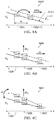
- FIG. 1B is a side view, e.g. in the (x,z) plane, of a portion of an example implementation of a haptic engine 150 that has a frame 152 .
- the haptic engine 150 includes, encapsulated inside the frame 152 , a mass 154 , a magnetic field source 156 and the IC chip 100 shown in FIG. 1A .
- the mass 154 can move relative to the frame 152 along the x-axis (e.g., through vibration left-and-right on page), along the z-axis (e.g., through vibration up-and-down on page), along the y-axis (e.g., through vibration in-and-out of page), or combinations of two or all three of these motions.
- the magnetic field source 156 includes portions 156 F that are disposed on (i.e., are “fixed” to) the frame 152 , e.g., coils, etc. As such, these are referred to as the fixed portions 156 F of the magnetic field source.
- coil sections 156 FA and 156 FB can be made from one winding (looped in and out of the page) and have continuous current flow.
- the magnetic field source 156 also includes portions 156 M that are part of the mass 154 , e.g., permanent magnets, etc. As these move along with the mass 154 , they are referred to as the mobile (or moving) portions 156 M of the magnetic field source.
- the mass 154 can be formed from a stainless steel cage with enclosures in which the mobile portions 156 M of the magnetic field source are held.
- a value of the mass 154 is a sum of a mass of all the mobile portions 156 M of the magnetic field source (e.g., the total mass of the mobile permanent magnets) and a mass of the stainless steel cage that holds them.
- a left magnet 156 MA is oriented with its north pole towards the top of the page and its south pole towards the bottom of the page
- a right magnet 156 MB is oriented with its north pole towards the bottom of the page and its south pole towards the top of the page.
- Coil sections 156 FA have the same electrical current flow (e.g., current IL)
- coil sections 156 FB have the opposite electrical current flow (e.g., current IL).
- current IL electrical current flow
- the coil 156 F experiences a Lorentz force to the left of the page and the magnets 156 M, along with the mass 154 , will move towards the right of the page.
- an alternating current IL that is provided through the coil 156 F causes a periodic Lorentz force that drives, along the x-axis, the mass 154 which includes the magnets 156 M.
- An amplitude and frequency of the displacement ⁇ X of the mass 154 is proportional to respective amplitude and frequency of the coil current IL.
- the fixed portions 156 F and the mobile portions 156 M of the magnetic field source are configured and arranged relative to each other, such that, when the mass 154 is at rest, the magnetic field source 156 as a whole emits a magnetic field B. Only two lines of a spatial distribution of the magnetic field B(X,Y,Z) emitted by the magnetic field source 156 is shown in FIG. 1B , however, more details of the spatial distribution of the magnetic field B(X,Y,Z) emitted by the magnetic field source 156 will be illustrated in FIGS. 2A, 3A-3B .
- the IC chip 100 is disposed on (i.e., is “fixed” to) the frame 152 of the haptic engine 150 in a sensing plane 105 of the spatial distribution of the magnetic field B(X,Y,Z) emitted by the magnetic field source 156 .
- each of the magnetic field sensing elements of the array 110 can determine one or more components of the magnetic field B, in the sensing plane 105 , at the respective locations 102 A, 102 B, 102 C.
- the fixed portions 156 F and the mobile portions 156 M of the magnetic field source are used both for driving the mass 154 along the x-axis and for sensing the mass' displacement ⁇ X along the x-axis, ⁇ Z along the z-axis, and ⁇ Y along the y-axis, as explained below.
- FIG. 1C is a side view, e.g. in the (x,z) plane, of a portion of another example implementation of a haptic engine 150 ′ that has a frame 152 ′.
- the haptic engine 150 ′ includes, encapsulated inside the frame 152 ′, a mass 154 ′, a magnetic field source 156 ′ and the IC chip 100 shown in FIG. 1A .
- the mass 154 ′ can move relative to the frame 152 ′ along the x-axis (e.g., through vibration left-and-right on page), along the z-axis (e.g., through vibration up-and-down on page), along the y-axis (e.g., through vibration in-and-out of page), or combinations of two or all three of these motions.
- the magnetic field source 156 ′ includes portions 156 ′F that are disposed on (i.e., are “fixed” to) the frame 152 ′, in this case, permanent magnets. As such, these are referred to as the fixed portions 156 ′F of the magnetic field source.
- the magnetic field source 156 ′ also includes portions 156 ′M that are part of the mass 154 ′, in this case, portions of a coil. As these move along with the mass 154 ′, they are referred to as the mobile (or moving) portions 156 ′M of the magnetic field source.
- coil sections 156 ′MA and 156 ′MB can be made from one winding (looped in and out of the page) and have continuous current flow.
- the mass 154 ′ can be formed from a stainless steel cage with enclosures in which the mobile portions 156 ′M of the magnetic field source are held.
- the magnetic field source 156 ′ also includes a marker magnet set 157 that can be attached to the stainless steel cage, for instance.
- the marker magnet set 157 can include one or more permanent magnets arranged in accordance with a predetermined pattern in the (x,y) plane.
- the permanent magnets of the marker magnet set 157 are arranged in a row in which adjacent ones have opposing polarities.
- a value of the mass 154 ′ is a sum of a mass of all the mobile portions 156 ′M of the magnetic field source (e.g., the mass of the portions of the mobile coil together with the mass of the marker magnet set 157 ) and a mass of the stainless steel cage that holds them.
- magnets 156 ′FA on the left side are oriented with their north pole towards the top of the page and their south pole towards the bottom of the page
- magnets 156 ′FB on the right side are oriented with their north pole towards the bottom of the page and their south pole towards the top of the page.
- Coil section 156 ′MA and coil section 156 ′MB have opposite respective electrical current flows (e.g., currents IL). For instance, when coil section 156 ′MA has current IL flowing out of the page and coil section 156 ′MB has current IL flowing into the page (as shown in FIG.
- an alternating current IL that is provided through the coil 156 ′M causes a periodic Lorentz force that drives, along the x-axis, the mass 154 ′ which includes the coil 156 ′M and the marker magnet set 157 .
- An amplitude and frequency of the displacement ⁇ X of the mass 154 ′ is proportional to respective amplitude and frequency of the coil current IL.
- the fixed portions 156 ′F and the mobile portions 156 ′M of the magnetic field source are configured and arranged relative to each other to emit, when the mass 154 ′ is at rest, a magnetic field B′.
- the marker magnet set 157 are configured to emit a marker magnetic field B M having a known spatial period ⁇ X between zero crossings thereof.
- the IC chip 100 is disposed on (i.e., is “fixed” to) the frame 152 ′ of the haptic engine 150 ′ in a sensing plane 105 ′ of the spatial distribution of the combined magnetic fields B′(X,Y,Z) and B M (X,Y,Z) emitted by the magnetic field source 156 as a whole.
- the marker magnet set 157 is spaced apart from the sensing plane 105 ′ such that, at the sensing plane, a strength of the marker magnetic field B M emitted by the marker magnet set 157 is 10 ⁇ , 100 ⁇ or 100 ⁇ stronger than a strength of the magnetic field B′ emitted by the combination of permanent magnets 156 ′F and coil 156 ′M of the magnetic field source.
- each of the magnetic field sensing elements of the array 110 can determine one or more components of the marker magnetic field B M , in the sensing plane 105 ′, at the respective locations 102 A, 102 B, 102 C.
- the magnets 156 ′F and the coil 156 ′M of the magnetic field source are used for driving the mass 154 ′ along the x-axis
- the marker magnet set 157 is used for sensing the mass' displacement ⁇ X along the x-axis, ⁇ Z along the z-axis, and ⁇ Y along the y-axis, as explained below.
- each magnetic field sensing element 110 ZA, 110 ZB, 110 ZC is a single-axial magnetic field sensing element configured to measure, at its respective location 102 A, 102 B, 102 C, a single component of a magnetic field B that is normal to the plane of the die 101 , e.g., component B Z along the z-axis.
- each of the single-axial magnetic field sensing elements 110 ZA, 110 ZB, 110 ZC can be a Hall-effect sensing element configured to measure the B Z component of a magnetic field B.
- each of the single-axial magnetic field sensing elements 110 ZA, 110 ZB, 110 ZC can be either a magneto-resistor or a flux-gate.
- each magnetic field sensing element 110 A, 110 B, 110 C is a tri-axial magnetic field sensing element configured to measure, at its respective location 102 A, 102 B, 102 C, all three components B Z , B X and B Y of a magnetic field B.
- the tri-axial magnetic field sensing element 110 A includes a combination of (i) a single-axial magnetic field sensing element 110 ZA configured to measure, at its location 102 A, a component B Z along the z-axis, (ii) a single-axial magnetic field sensing element 110 XA configured to measure, at its location 102 A, a component B X along the x-axis, and (iii) a single-axial magnetic field sensing element 110 YA configured to measure component B Y along the y-axis.
- each of the tri-axial magnetic field sensing elements 110 A, 110 B, 110 C can be a tri-axial Hall-effect sensing element configured to measure the B Z , B X and B Y components of a magnetic field B.
- FIG. 2A is a cross-section 158 in the plane (x,z) of a portion of an example of the spatial distribution of the magnetic field B(X,Y,Z) emitted by the magnetic field source 156 .
- the sensing plane 105 also is overlaid, in FIG. 2A , on the (x,z) cross-section 158 of the spatial distribution of the magnetic field B(X,Y,Z). Note that, at a location 102 A of the sensing plane 105 , where one of the magnetic field sensing elements of the array 110 is disposed, the magnetic field B has non-zero B Z , B X and B Y components.
- FIG. 2B shows components B Z ( 102 A), B X ( 102 A), B Y ( 102 A) of the magnetic field B measured at location 102 A where the tri-axial Hall-effect sensing element 110 A is located.
- FIG. 3A is a representation of a spatial distribution 160 Z of the axial component B Z (X,Y) along the z-axis of the magnetic field B, measured in the sensing plane 105 (e.g., parallel to the (x,y) plane).
- a component B X (X,Y) along the x-axis and a component B Y (X,Y) along the y-axis of the magnetic field B are measured concurrently with the component B Z (X,Y), in the same sensing plane 105 .
- FIG. 3C shows a first cross-section 162 X of the representation of the spatial distribution 160 Z of the axial component B Z (X,Y) and a second cross-section 163 X of the representation of the spatial distribution 160 XY of the transverse component B XY (X,Y).
- Each of the cross-sections 162 X, 163 X corresponds to the segment AB parallel to the x-axis and spans a first region (denoted I) adjacent to first end point A, a second region (denoted II) between intermediate points P 1 , P 2 , and a third region (denoted III) adjacent to second end point B.
- the first cross-section 162 X is linear in Region II, where it has large slope ⁇ B Z / ⁇ X, and non-linear in each of Regions I, III, where it has nearly zero slope ⁇ B Z / ⁇ X but large curvature ⁇ 2 B Z / ⁇ X 2 .
- a measurement of the displacement ⁇ X, performed based on the spatial distribution 160 Z of the axial component B Z (X,Y) has highest sensitivity, that is proportional to ⁇ B Z / ⁇ X, in Region II.
- the sensitivity of the measurement of the displacement ⁇ X, performed based on the same spatial distribution 160 Z of the axial component B Z (X,Y) is proportional to ⁇ 2 B Z / ⁇ X 2 in Region I and Region III.
- the second cross-section 163 X is linear in each of Regions I, III, where it has large slope ⁇ B XY / ⁇ X, and non-linear in Region II, where it has nearly zero slope ⁇ B XY / ⁇ X but large curvature ⁇ 2 B XY / ⁇ X 2 .
- a measurement of the displacement ⁇ X, performed based on the spatial distribution 160 XY of the transverse component B XY (X,Y) has highest sensitivity, that is proportional to ⁇ B XY / ⁇ X, in Region I and Region III.
- the sensitivity of the measurement of the displacement ⁇ X performed based on the same spatial distribution 160 XY of the transverse component B XY (X,Y) is proportional to ⁇ 2 B XY / ⁇ X 2 in Region II.
- a third cross-section of the representation of the spatial distribution 160 Z of the axial component B Z (X,Y), that corresponds to the segment CD parallel to the y-axis, is linear between intermediate point P 3 and end point D, where it has large slope ⁇ B Z / ⁇ Y, and non-linear in between intermediate point P 3 and end point C, where it has nearly zero slope ⁇ B Z / ⁇ Y but large curvature ⁇ 2 B Z / ⁇ Y 2 .
- a measurement of the displacement ⁇ Y performed based on the spatial distribution 160 Z of the axial component B Z (X,Y), has highest sensitivity, that is proportional to ⁇ B Z / ⁇ Y, point P 3 and end point D.
- motion of the mass 154 that includes at least one of a displacement ⁇ X along the x-axis, a displacement ⁇ Z along the z-axis, and a displacement ⁇ Y along the y-axis, causes rearrangement of the fixed portions 156 FA, 156 FB and mobile portions 156 MA, 156 MB of the magnetic field source with respect to each other.
- the magnetic field B emitted by the magnetic field source 156 as a whole will change as its mobile portions 156 MA, 156 MB are moving, along with the mass 154 , relative to its fixed portions 156 FA, 156 MB.
- the magnetic field sensing elements of the array 110 will measure, at their respective asymmetrically distributed locations 102 A, 102 B, 102 C in the sensing plane 105 , the changes of the magnetic field B caused by the motion of the mass 154 .
- the DSP 122 of the mix-signal circuitry 120 uses the changes of the magnetic field B, measured by the magnetic field sensing elements of the array 110 at their respective asymmetrically distributed locations 102 A, 102 B, 102 C in the sensing plane 105 , to determine one or more of the displacements ⁇ X, ⁇ Z, and ⁇ Y of the mass 154 .
- the displacements ⁇ X, ⁇ Z, and ⁇ Y of the mass 154 are determined by the DSP 122 with an accuracy corresponding to the accuracy of lithography processes used to establish/form the separations d 1 and d 2 .
- the separation d 2 between the magnetic field sensing elements 110 B and 110 C has to be larger than the separation d 1 between the magnetic field sensing elements 110 A and 110 B by at least 2%, 5% or 10%, so the displacements ⁇ X, ⁇ Z, and ⁇ Y are measurable in accordance with the techniques described herein.
- the separation d 1 between the magnetic field sensing elements 110 A and 110 B is in a range of 10-100 ⁇ m, and the separation d 2 between the magnetic field sensing elements 110 B and 110 C is suitably 2 ⁇ -10 ⁇ larger than d 1 .
- the first magnetic field sensing element 110 ZA measures the component B Z ( 102 A) of the magnetic field at the first location 102 A
- the second magnetic field sensing element 110 ZB measures the component B Z ( 102 B) of the magnetic field at the second location 102 B.
- d 1 is the separation along the x-axis between the first location 102 A, where the first magnetic field sensing element 110 ZA is located, and the second location 102 B, where the second magnetic field sensing element 110 ZB is located.
- a displacement ⁇ Z along the z-axis and a displacement ⁇ X along the x-axis of the mass 154 induce a change of the component ⁇ B Z ( 102 A) at the first location 102 A and a change of the component ⁇ B Z ( 102 B) at the second location 102 A in accordance with the following system of two linear equations:
- [ ⁇ ⁇ ⁇ B Z ⁇ ( 102 ⁇ A ) ⁇ ⁇ ⁇ B Z ⁇ ( 102 ⁇ B ) ] [ ⁇ ⁇ ⁇ B Z ⁇ ( 102 ⁇ A ) ⁇ ⁇ ⁇ B Z ⁇ ( 102 ⁇ ⁇ A ) ⁇ ⁇ ⁇ X ⁇ ⁇ ( B Z ⁇ ( 102 ⁇ A ) + d 1 ⁇ ⁇ ⁇ ⁇ B Z ⁇ ( 102 ⁇ A ) ⁇ ⁇ ⁇ X ) ⁇ ⁇ ⁇ B Z ⁇ ( 102 ⁇ B ) ⁇ ⁇ ⁇ X ] ⁇ [ ⁇ ⁇ ⁇ Z ⁇ ⁇ ⁇ X ] .
- the DSP 122 is configured to solve the above system of linear equations for the two unknown displacements ⁇ Z, ⁇ X and unknown parameter a in terms of the measured changes ⁇ B Z ( 102 A) and ⁇ B Z ( 102 B). Note that, in view of the above noted linear approximation, the magnetic flux gradient satisfies the following first condition:
- the DSP 122 can infer, without having to perform a calibration based on an external displacement reference, that the mass 154 has traveled, over the time z, exactly the separation d 1 between the first and second magnetic field sensing elements.
- the DSP 122 is configured to substitute EQs. 8-9 into the system of linear equations of EQ. 7 to determine the following displacement ⁇ Z along the z-axis:
- equations EQs. 7-10 can be generalized to account for the remaining magnetic field sensing elements of the array 110 , e.g., the third magnetic field sensing element 110 ZC that is separated from the second magnetic field sensing element 110 ZB by separation d 2 .
- a change ⁇ B Z at a location where the component B Z has a small magnitude is equal to another change ⁇ B Z at another location where the component B Z has a large magnitude.
- a change ⁇ B Z at a location where the component B Z has a small magnitude is smaller than another change ⁇ B Z at another location where the component B Z has a large magnitude.
- a separation d n between locations of magnetic field sensing elements is small (e.g., like the separation d 1 between the second magnetic field sensing element 110 ZB and the first magnetic field sensing element 110 ZA), then it cannot be distinguished whether the measured changes ⁇ B Z ( 102 n ) and ⁇ B Z ( 102 ( n +1)) were caused by a displacement ⁇ Z along the z-axis or a displacement ⁇ X along the x-axis, because it is likely that the magnitudes of B Z ( 102 n ) and B Z ( 102 ( n +1)) are about the same at nearby locations.
- magnetic field sensing elements that are separated by a large separation d n will be used to determine a displacement ⁇ Z of the mass 154 .
- a displacement ⁇ Z of the mass 154 can be estimated with fine resolution using EQ. 10.
- magnetic field sensing elements that are separated by a small separation d n (e.g., like separation d 1 between the adjacent first and second magnetic field sensing elements 110 ZA, 110 ZB) will be used to determine a displacement ⁇ X of the mass 154 .
- the DSP 122 can perform determinations of a displacement ⁇ Y of the mass 154 along the y-axis by generalizing EQ. 6-10.
- the nonlinearity of a cross-section along the segment CD parallel to the y-axis of the representation of the spatial distribution 160 Z of the axial component B Z (X,Y) suggests that (i) determination of a displacement ⁇ Y along the y-axis is sensitive to the curvature of the cross-section along the segment CD between end point C and point P 3 , and (ii) determination of ⁇ Y is sensitive to the slope of the cross-section along the segment CD between point P 3 and end point D.
- a magnetic field sensing element to be used for determining the ⁇ Y displacement will be disposed between the center and the edge of the die 101 , where a value of ⁇ B Z / ⁇ Y is expected to be largest. This is shown in FIG. 1A , where the magnetic field sensing elements 110 ZA, 110 ZB, 110 ZC are off-centered along the width of the die 101 .
- values of the gradient ⁇ B Z / ⁇ X at various locations of the die 101 where the magnetic field sensing elements of the array 110 are disposed are measured as part of a calibration procedure described below. A procedure to equalize sensitivity of the magnetic field sensing elements of the array 110 is described first.
- FIG. 5A is a flow chart of an example of a process 500 used to equalize sensitivity across the magnetic field sensing elements of the array 110 of the IC chip 100 when the latter is part of the haptic engine 150 .
- each magnetic field sensing element 110 Zn where n is ⁇ A, B, C, . . . ⁇ , is a Hall-effect sensing element that transduces a magnitude and direction of a component B Z ( 102 n ) of the magnetic field along the z-axis, at the Hall-effect sensing element's location 102 n , to a Hall voltage V( 102 n ).
- the process 500 is performed by at least one of the circuits of the mix-signal circuitry 120 , and by controller circuitry of the haptic engine 150 .
- the fixed portions 156 FA, 156 FB of the magnetic field source (e.g., the coils A and B) of the haptic engine 150 are driven at high frequency with known coil current I L0 ⁇ 0, to avoid moving the mobile portions 156 MA, 156 MB of the magnetic field source (e.g., the permanent magnets A and B).
- a respective Hall voltage v( 102 n ;t 2 ) at a corresponding location 102 n is measured, at time t 2 , on each of the n Hall-effect sensing elements of the array 110 .
- sensitivity across all n Hall-effect sensing elements of the array 110 is equalized, by adjusting their gain, so v( 102 n ;t 2 ) ⁇ v( 102 n ;t 1 ) is the same for all n Hall-effect sensing elements. This ensures that each Hall-effect sensing element 110 Zn will output the same value of the Hall voltage V( 102 n ) when the Hall-effect sensing element senses the same field.
- EM electromagnetic
- FIG. 5B is a flow chart of a calibration process 530 used for determining a gradient ⁇ B Z / ⁇ X at the sensing plane 105 of the haptic engine 150 .
- each magnetic field sensing element 110 Zn where n is ⁇ A, B, C, . . . ⁇ , is a Hall-effect sensing element that measures a magnitude and direction of a component B Z ( 102 n ) of the magnetic field along the z-axis at the Hall-effect sensing element's location 102 n .
- the process 500 is performed by at least one of the circuits of the mix-signal circuitry 120 , and by controller circuitry of the haptic engine 150 .
- the haptic engine 150 which is a linear resonant actuator (LRA) is driven with sinusoidal input voltage at resonance. While 535 is in progress, the following operations are performed.
- LRA linear resonant actuator
- the gradient ⁇ BZ/ ⁇ X at a location 102 ( n +0.5) between locations 102 n and 102 ( n +1) that are separated by a separation d n is estimated geometrically, in accordance with FIG. 5C , in the following manner:
- a value of B Z as a function, X(B), over the position along the x-axis in a range from B 1 to B 2 is estimated by integrating over the inverse of the determined gradient 1/( ⁇ B Z / ⁇ X) in the following manner:
- X ⁇ ( B ) ⁇ B ⁇ ⁇ 1 B ⁇ ⁇ 2 ⁇ 1 ( ⁇ ⁇ ⁇ B Z ⁇ ⁇ ⁇ X ) ⁇ dB Z . ( 12 )
- the determined function X(B) can be used to map every measured value of B Z (for instance B Z ( 102 n ) at location 102 n ) to a unique value of X.
- FIG. 5D shows a look up table (LUT) 546 , shown here as a graph of X vs.
- B Z that stores an example of a set of pairs of estimated positions X(B Z ) of the moving mass 154 , between X MIN and X MAX , and corresponding measured values of the magnetic field component B Z , between B ZMIN and B ZMAX , obtained based on EQ. 12.
- B Z (m) the position of the moving mass 154 can be estimated by simply reading from LUT 546 a value X(m) corresponding to the measured value B Z (m).
- a displacement of the mass 154 is referenced by a combination of geometries of the IC chip 100 and of the haptic engine 150 (e.g., separations d 1 , d 2 , etc. between magnetic field sensing element 110 ZA, 110 ZB, etc. of the array 110 ) rather than geometry of an external tester.
- the positions of the mass 154 estimated from LUT 546 based on measurements of the magnetic field component B Z corresponds to a “macroscopic motion” of the mass, e.g., over 10s or 100s of microns.
- the DSP 122 can determine displacements ⁇ Z and ⁇ X of the moving mass 154 that correspond to its “microscopic motion”, e.g., at a sub-micron or micron scale, by using the gradient ⁇ BZ/ ⁇ X that has been determined in accordance with the process 530 , as described below.
- FIG. 5E is a flow chart of a process 550 used during run-time of the IC chip 100 to determine displacements ⁇ Z and ⁇ X of a mass 154 , where the mass and the IC chip are part of the haptic engine 150 , and the IC chip is disposed at a sensing plane 105 of the haptic engine.
- the displacements ⁇ Z and ⁇ X correspond to microscopic motion riding on macroscopic motion, the latter causing the mass 154 to sweep through locations X(B), in accordance with EQ. 12 and LUT 546 .
- ⁇ is a Hall-effect sensing element that measures a magnitude and direction of a component B Z ( 102 n ) of the magnetic field along the z-axis at the Hall-effect sensing element's location 102 n .
- the process 550 is performed by the DSP 122 of the mix-signal circuitry 120 .
- the process 550 uses sensors at more than 2 locations 102 n with different separations, d n (and hence different sensitivities of the measurements of displacement ⁇ Z and displacement ⁇ X, respectively, according to EQs. 7-10), to simultaneously solve for the displacements ⁇ Z and ⁇ X.
- a displacement ⁇ Z( ⁇ ) along the z-axis is estimated using two magnetic field sensing elements of the array 110 disposed at locations spaced apart by a large separation, in accordance with EQ. 10, and using the gradient ⁇ BZ/ ⁇ X determined based on the process 530 .
- changes ⁇ B Z measured by the second magnetic field sensing element 110 ZB and the third magnetic field sensing element 110 ZC at the respective second location 102 B and third location 102 C that are separated by a separation d 2 can be used for the estimation performed at 555 .
- changes ⁇ B Z measured by the first magnetic field sensing element 110 ZA and the third magnetic field sensing element 110 ZC at the respective first location 102 A and third location 102 C that are separated by a separation d 1 +d 2 can be used for the estimation performed at 555 .
- parameter a and a displacement ⁇ X along the x-axis of the mass 154 are determined using two magnetic field sensing elements of the array 110 disposed at locations spaced apart by a small separation and the gradient ⁇ BZ/ ⁇ X determined based on the process 530 .
- changes ⁇ B Z measured by the first magnetic field sensing element 110 ZA and the second magnetic field sensing element 110 ZB at the respective first location 102 A and second location 102 B that are separated by a separation d 1 can be used for the determination performed at 560 .
- This determination is performed by inverting EQ. 7 in the following manner:
- [ ⁇ ⁇ ⁇ ⁇ X ] [ ⁇ ⁇ ⁇ ZB Z ⁇ ( 102 ⁇ A ) ⁇ ⁇ ⁇ B Z ⁇ ( 102 ⁇ A ) ⁇ ⁇ ⁇ X ⁇ ⁇ ⁇ Z ⁇ ( B Z ⁇ ( 102 ⁇ A ) + d 1 ⁇ ⁇ ⁇ ⁇ B Z ⁇ ( 102 ⁇ A ) ⁇ ⁇ ⁇ X ) ⁇ ⁇ ⁇ B Z ⁇ ( 102 ⁇ B ) ⁇ ⁇ ⁇ X ] - 1 ⁇ [ ⁇ ⁇ ⁇ B Z ⁇ ( 102 ⁇ A ) ⁇ ⁇ ⁇ ⁇ B Z ⁇ ( 102 ⁇ B ) ] . ( 13 ) Note that EQs. 10 and 13 constitute a system of three linear equations with three unknowns a, ⁇ Z, ⁇ X. Such system of linear equations can have a unique solution.
- the motion of the mass 154 of the haptic engine 150 can be sensed based on the angle ang(B) formed by the magnetic field with the z axis, instead of based on the component B Z along the z-axis of the magnetic field.
- the angle ang(B) is determined by the DSP 122 , based on the spatial distribution 160 Z of the axial component B Z (X,Y) shown in FIG. 3A and the spatial distribution 160 XY of the transverse component B XY (X,Y) shown in FIG. 3B , as
- ang ⁇ ( B ) ⁇ ( X , Y ) tan - 1 ⁇ ( B Z ⁇ ( X , Y ) B XY ⁇ ( X , Y ) ) .
- the transverse component B XY (X,Y) is obtained by the DSP 122 using EQ. 6.
- orientation of ang(B) at the sensing plane 105 corresponds to orientation of the magnetic field lines thereat.
- the displacements ⁇ X and ⁇ Z of the mass 154 in terms of changes ⁇ [ang(B)] of the magnetic field angle ang(B), can be determined by solving EQs. 7-13, where ⁇ [ang(B)] is substituted for ⁇ B Z .
- the displacements ⁇ X and ⁇ Z of the mass 154 can now be encoded in angular domain, so they can be determined based on a ratio-metric measurement of the magnetic field angle ang(B), in accordance with EQ. 14.
- determinations of the displacements ⁇ X and ⁇ Z of the mass 154 are based on a ratio-metric measurement, results of these determinations are insensitive to temperature change.
- processes 530 and 550 can be used, in a manner similar to the one described above in connection with FIGS. 5B-5E , to determine the displacements ⁇ X and ⁇ Z of the mass 154 based on the changes ⁇ [ang(B)] measured by the tri-axial Hall-effect sensing elements 110 A, 110 B, 110 C.
- the DSP 122 uses first the process 530 to determine the gradient ⁇ [ang(B)]/ ⁇ X, and then the process 550 to determine the displacements ⁇ X and ⁇ Z of the mass 154 based on the determined gradient ⁇ [ang(B)]/ ⁇ X.
- each instance of an input set of values of measured magnetic field B Z or measured change ⁇ B Z of the magnetic field results in an output set of values of the position X and displacements ⁇ X and ⁇ Z that is independent of other output sets of values of the position X and displacements ⁇ X and ⁇ Z that have been previously obtained from respective sets of previously measured magnetic field B Z or measured change ⁇ B Z of the magnetic field.
- FIG. 5F shows a state-observer feedback control system 570 that includes uses the array 110 of magnetic field sensing elements, e.g., described above in connection with FIG. 1A , look-up-table (LUT) 572 , a state-observer 574 , a controller 576 and the haptic engine 150 (that includes the mass 154 , the magnetic field source 156 , etc.)
- LUT look-up-table
- the state-observer feedback control system 570 uses the array 110 of magnetic field sensing elements to measure various magnetic field components B X (k), B Y (k), B Z (k) at a respective position 102 A, 102 B, etc. of each sensor 110 A, 110 B, etc. These measured values are used to interpolate LUT 572 to generate a measured plant output y[k].
- the plant is the haptic engine 150
- x[k] is a state of the haptic engine.
- the state x[k] of the haptic engine includes a current X position of the mass 154 .
- the plant output y[k] represents a measured X position of the mass 154 given its current position x[k] and a driving signal u[k] acting on the mass.
- the driving signal u[k] can be a coil current I L .
- the LUT 572 can be calibrated using a reference sensor.
- a laser profiler can be used to measure the X position (y[k] state is the X position, in this case) of the engine 150 's moving mass 154 while the engine is actuated.
- a set of B field measurements is collected by the sensor array 110 over this set of known y[k] states and the LUT 572 is generated to lookup y[k] for a given set of B field measurements.
- the state observer 574 obtains an estimate of the next engine state ⁇ circumflex over (x) ⁇ [k+1] based on a current estimate of the same, a current estimate of the engine output ⁇ [k], and a discrepancy between the output measurements y[k] and the output estimate ⁇ [k].
- the estimated engine state ⁇ circumflex over (x) ⁇ [k] along with an input command are used by the controller 576 to provide a drive signal u[k].
- the drive signal u[k] is returned to the state observer 574 through a feedback loop, where it is used by the state observer 574 as a second input along with the first input noted above. Additionally, the drive signal u[k] is provided to the engine 150 having an engine state x[k].
- the IC chip 100 can be modified in various ways and then used in the haptic engine 150 to determine a displacement ⁇ Y along the y-axis of the mass 154 concurrently with determining the displacements ⁇ X and ⁇ Z thereof.
- FIG. 6 is a plan view, e.g., in the (x,y) plane, of an example of a modified IC chip 600 that includes an array 610 of magnetic field sensing elements, an array of contact pads 666 , and mix-signal circuitry 620 formed on a die 601 .
- the magnetic field sensing elements of the array 610 are distributed on the die 601 along two rows extending along a first direction. e.g., along the x-axis.
- some of the magnetic field sensing elements of the array 610 are disposed at locations 602 A, 602 B, 602 C along the first row, and at locations 602 E, 602 G along the second row, for instance.
- the second location 602 B is between the first location 602 A and the third location 602 C, and the second location is separated from the first location by a first distance d 1 and from the third location by a second distance d 2 different from the first distance. Moreover, the first and second rows are separated from each other by a third distance d 3 .
- the mix-signal circuitry 620 is disposed in a central area 604 of the die 601 that separates, along the x-axis, the second location 602 B and the third location 602 C on the first row, as well as the fourth location 602 E and the fifth location 602 G on the second row.
- the second distance d 2 is larger than the first distance d 1
- the magnetic field sensing elements of the array 610 are said to be asymmetrically distributed along the x-axis.
- each magnetic field sensing element 610 ZA, 610 ZB, 610 ZC, 610 ZE, 610 ZG is a single-axial magnetic field sensing element configured to measure, when the IC chip 600 is disposed in the sensing plane 105 of the haptic engine 150 , at its respective location 602 A, 602 B, 602 C, 602 E, 602 G, the B Z component of the magnetic field B.
- each magnetic field sensing element 610 A, 610 B, 610 C, 610 E, 610 G is a tri-axial magnetic field sensing element configured to measure, when the IC chip 600 is disposed in the sensing plane 105 of the haptic engine 150 , at its respective location 602 A, 602 B, 602 C, 602 E, 602 G, all three components B Z , B X and B Y of a magnetic field B.
- the tri-axial magnetic field sensing element 610 A includes a combination of (i) a single-axial magnetic field sensing element 610 ZA configured to measure, at its location 602 A, a component B Z along the z-axis, (ii) a single-axial magnetic field sensing element 610 XA configured to measure, at its location 602 A, a component B X along the x-axis, and (iii) a single-axial magnetic field sensing element 610 YA configured to measure component B Y along the y-axis.
- the array 610 of magnetic field sensing elements of the IC chip 600 is used to measure changes in the magnetic field, e.g., ⁇ B Z or ⁇ [ang(B)], at respective locations of the magnetic field sensing elements, such that determinations of both displacement ⁇ X along the x-axis and displacement ⁇ Y along the y-axis can be performed concurrently with determinations of displacement ⁇ Z along the z-axis of the mass 154 .
- magnetic field sensing elements, at the locations 102 A, 102 C separated by d 1 +d 2 on the first row are used by the DSP 622 of the mix-signal circuitry 620 to determine displacement ⁇ Z of the mass 154 using EQ.
- magnetic field sensing elements at the locations 102 A, 102 B separated by d 1 on the first row, are used by the DSP 622 to determine displacement ⁇ X of the mass 154 using EQs. 8 and 11; and magnetic field sensing elements, at the locations 102 A, 102 E separated by d 3 between the first and second rows, are used by the DSP 622 to determine displacement ⁇ Y of the mass 154 using equations similar to EQs. 8 and 11.
- FIG. 7 is a plan view, e.g., in the (x,y) plane, of another example of a modified IC chip 700 that includes an array 710 of magnetic field sensing elements, an array of contact pads 766 , and mix-signal circuitry 720 formed on a die 701 .
- the magnetic field sensing elements of the array 710 are distributed on the die 701 along two rows extending along a first direction. e.g., along the x-axis.
- some of the magnetic field sensing elements of the array 710 are disposed at locations 702 A, 702 B, 702 C, 702 D along the first row, and at locations 702 E, 702 F, 702 G, 702 H along the second row, for instance.
- the second location 702 B (the sixth location 702 F) is between the first location 702 A (the fifth location 702 E) and the third location 702 C (the seventh location 702 G), and the second location (the sixth location) is separated from the first location (the fifth location) by a first distance d 1 and from the third location (the seventh location) by a second distance d 2 different from the first distance. Also, the third location (the seventh location) is separated from the fourth location (the eighth location) by the same first distance d 1 . Moreover, the first and second rows are separated from each other by a third distance d 3 .
- the mix-signal circuitry 720 is disposed in a central area 704 of the die 701 that separates, along the x-axis, the second location 702 B and the third location 702 C on the first row, as well as the sixth location 702 F and the seventh location 702 G on the second row.
- the magnetic field sensing elements of the array 710 are said to be symmetrically distributed along the x-axis.
- each magnetic field sensing element 710 ZA, 710 ZB, 710 ZC, 710 ZD, 710 ZE, 710 ZF, 710 ZG, 710 ZH is a single-axial magnetic field sensing element configured to measure, when the IC chip 700 is disposed in the sensing plane 105 of the haptic engine 150 , at its respective location 702 A, 702 B, 702 C, 702 D, 702 E, 702 F, 702 G, 702 H the B Z component of the magnetic field B.
- each magnetic field sensing element 710 A, 710 B, 710 C, 710 D, 710 E, 710 F, 710 G, 710 H is a tri-axial magnetic field sensing element configured to measure, when the IC chip 700 is disposed in the sensing plane 105 of the haptic engine 150 , at its respective location 702 A, 702 B, 702 C, 702 D, 702 E, 702 F, 702 G, 702 H, all three components B Z , B X and B Y of a magnetic field B.
- the tri-axial magnetic field sensing element 710 A includes a combination of (i) a single-axial magnetic field sensing element 710 ZA configured to measure, at its location 702 A, a component B Z along the z-axis, (ii) a single-axial magnetic field sensing element 710 XA configured to measure, at its location 702 A, a component B X along the x-axis, and (iii) a single-axial magnetic field sensing element 710 YA configured to measure component B Y along the y-axis.
- the array 710 of magnetic field sensing elements of the IC chip 700 is used to measure, at respective locations of the magnetic field sensing elements, changes ⁇ B Z (or ⁇ [ang(B)]) in the magnetic field.
- the DSP 722 can determine curvature of the spatial distribution 160 XY of the transverse component B XY (X,Y) of the magnetic field, e.g., in terms of ⁇ 2 B Z / ⁇ X 2 .
- changes ⁇ B Z measured by magnetic field sensing elements disposed on the first row, at locations 702 A, 702 B separated by d 1 , on one side of the central area 704 are used by the DSP 722 to determine a first instance of ⁇ B Z / ⁇ X; and changes ⁇ B Z measured by magnetic field sensing elements disposed on the first row, at locations 702 C, 702 D also separated by d 1 , on the opposing side of the central area 704 , are used by the DSP 722 to determine a second instance of ⁇ B Z / ⁇ X.
- EQ. 2 can be modified to include quadratic changes in the magnetic field, e.g., ⁇ 2 B Z / ⁇ X 2 , which are measured by the IC chip 700 as explained above.
- the DSP 722 can determine displacement ⁇ Z along the z-axis and displacement ⁇ X along the x-axis from EQs. 2 and 6-11 appropriately modified to include quadratic terms ⁇ 2 B Z / ⁇ X 2 .
- the magnetic field sensing elements of their respective arrays 110 , 610 , 710 on both sides of respective mixed-signal circuitry 120 , 620 , 720 makes efficient use of the silicon real-estate while producing a large value of the separation d n between at least some of the magnetic field sensing elements.
- the magnetic field sensing elements that are asymmetrically disposed in the X or Y directions are beneficially used for measuring changes in the magnetic field, e.g., ⁇ B Z or ⁇ [ang(B)], so the measured changes in the magnetic field can then be used for accurately determining the displacement ⁇ Z.
- FIG. 8 is a circuit diagram of an example of mix-signal circuitry 820 integrated together with multiple magnetic field sensing elements on an IC chip that is implemented as an ASIC.
- each of the magnetic field sensing elements is implemented as a uniaxial Hall-effect sensing element.
- Any one of the IC chips 100 , 600 , 700 described above in connection with FIGS. 1A, 6, 7 , respectively, can be implemented as the ASIC shown in FIG. 8 .
- the ASIC shown in FIG. 8 can be placed in the sensing plane 105 of the haptic engine 150 that includes mass 154 .
- the ASIC chip includes one or more driving circuits 826 P, 826 R, etc.
- Each driving circuit 826 P (or 826 R, etc.) includes a programmable current source 826 P (or 826 R, etc.), two or more Hall-effect sensing elements, and a dummy load 828 P (or 828 R, etc.) connected to each other in series.
- the programmable current source 826 P (or 826 R, etc.) can be implemented as a single current steered DAC.
- a single current source 826 P (or 826 R, etc.) can be shared between 2 or more sensors.
- a single current source can be shared by 110 XA, 110 YA, and 110 ZA.
- This grouping in series of the driving circuit 826 P can cause power savings, as Hall-effect sensing elements are conventionally connected in parallel, each with its own current source, which consumes a lot of power.
- the dummy load 828 P (or 828 R, etc.) is a reference resistor with known resistance for calibrating a respective current source 826 P (or 826 R, etc.)
- CMOS complementary-metal-oxide-semiconductor
- Such a dummy load resistor can be fabricated in modern complementary-metal-oxide-semiconductor (CMOS) technologies using gate-poly-silicon, doped silicon, biased transistor (in linear region), etc.
- CMOS complementary-metal-oxide-semiconductor
- the mix-signal circuitry 820 further includes a band-gap reference circuit 830 .
- a temperature insensitive background calibration can be performed by comparing the voltage across the dummy loads 828 P, 828 R, etc., against the single band-gap reference circuit 830 .
- the mix-signal circuitry 820 further includes sample-and-hold (S/H) circuits 834 , each of the S/H circuit including a capacitor.
- S/H sample-and-hold
- the S/H circuitry 834 allows global shutter capture which reduces motion blur.
- the mix-signal circuitry 820 further includes, for each of the driving circuits, an analog multiplexer circuit 832 P (or 832 R, etc.), a programmable gain amplifier (PGA) circuit 836 P (or 836 R, etc.), and an analog to digital converter (ADC) circuit 840 P (or 840 R, etc.)
- the analog multiplexer circuit 832 includes input ports and an output port, wherein an output of each of the corresponding magnetic field sensing elements, the respective dummy 828 P (or 828 R, etc.), and the band-gap reference circuit 830 is coupled with a respective input port of the analog multiplexer circuit through a respective sample and hold circuit 834 .
- analog multiplexer circuit 832 P (or 832 R, etc.) is bootstrapped to (1) provide random-access from the Hall-effect sensing elements to the parallel PGA circuits 836 P, 836 R, etc., and (2) reduce parasitic charge transfer in large (W/L) high-speed field-effect transistors (FETs).
- This multiplexer is functionally defined to have multiple inputs and multiple outputs, and routing between a specified input and a specified output is selected by a corresponding address input. In terms of circuit realization, such a multiplexer can be realized by a plurality of multiplexer modules 832 P, 832 R, etc., one for each of the programmable amplifiers 836 P, 836 R, etc.
- Each one of the multiplexer modules 832 P, 832 R, etc. will have only one output that feeds into one of the PGA/ADC channels 836 P/ 840 P, 836 R/ 840 R, etc.
- Each one of the sample and hold circuits 834 will feed into one of the inputs on one of these multiplexer modules 832 P, 832 R, etc.
- the address input for each multiplexer module 832 P, 832 R, etc. can be shared or individually addressed.
- the PGA circuit 836 P (or 836 R, etc.) is coupled with the output port of the analog multiplexer circuit 832 P (or 832 R, etc.) Note that the S/H circuitry 834 also level shifts the Hall voltage output by each of the Hall-effect sensing elements to input common-mode (CM) level of the PGA circuit 836 P (or 836 R, etc.)
- CM common-mode
- the mix-signal circuitry 820 further includes a pair of multiplexers 838 P (or 838 R, etc.), also referred to as a chopping multiplexer pair, that includes a first multiplexer coupled between the output port of the analog multiplexer circuit 832 P (or 832 R, etc.) and the input port of PGA circuit 836 P (or 836 R, etc.) and a second multiplexer coupled between the output port of the PGA circuit 836 P (or 836 R, etc.) and the input port of ADC circuit 840 P (or 840 R, etc.).
- the ADC circuit 840 P (or 840 R, etc.) is coupled between the PGA circuit 836 P (or 836 R, etc.) and the DSP 822 .
- the multiple PGA circuit 836 P (or 836 R, etc.) and ADC circuit 840 P (or 840 R, etc.) channels are being parallelized to increase sampling speed and relax analog design requirement.
- the mix-signal circuitry 820 includes a DSP 822 coupled with the ADC circuits 840 P, 840 R, etc.
- the DSP 822 can be implemented as a FPGA, or MCU, or any digital state-machine, for instance, and configured to perform any one of the techniques described above (e.g., processes 530 , 550 ) for determining displacements ⁇ Z, ⁇ X and ⁇ Y of the mass 154 based on changes of a magnetic field measured by the Hall-effect sensing elements included in the ASIC.
- the determined displacements ⁇ Z, ⁇ X and ⁇ Y can be output to an off-chip computing system 842 for further processing, storing, etc.
- Another advantage of the technologies described above is that only digital information is communicated between the DSP 822 and the off-chip computing system 842 .
- This interface between the DSP 822 and the off-chip computing system 842 can be implemented using the pads 666 shown in FIG. 6 or the pads 766 shown in FIG. 7 .
- only a small number of pads is provided on IC chip 600 or 700 for high speed digital data transmission, which can save cost relative to some conventional implementations of magnetic field sensing systems in which an analog signal is output by each sensor to an off-chip computing system, such that a pair of pads needs to be provided for each sensor.
- the architecture of the mix-signal circuitry 820 relies on ⁇ B sensing which inherently cancels out a Hall voltage offset output by the Hall-effect sensing elements of the ASIC shown in FIG. 8 .
- Low-frequency noise is minimized when a sampling speed is high enough to ensure time correlation between the two samples that generate ⁇ B.
- processes 530 and 550 can be used to encode one or more displacements ⁇ X, ⁇ Y, and ⁇ Z of a mass 154 of a haptic engine 150 in magnetic field intensity along one axis, e.g., B Z (or alternatively B X or B Y ), and measuring it via uniaxial Hall-effect sensing elements (or other uniaxial magnetic field sensing elements.)
- Self-calibration of mass 154 's displacement can be performed by determining a gradient ⁇ B Z / ⁇ X based on the known distance, dn, between uniaxial Hall-effect sensing elements.
- Discriminating the displacements ⁇ X, ⁇ Y, and ⁇ Z during runtime can be performed by using (i) changes ⁇ B Z measured by different combinations of uniaxial Hall-effect sensing elements with different separation distances, d n , and (ii) self-calibration data relating to the gradient ⁇ B Z / ⁇ X to solve for each motion component separately. Same processes can be used based on gradient ⁇ B X / ⁇ X or gradient ⁇ B Y / ⁇ X.
- processes 530 and 550 can be used to encode one or more displacements ⁇ X, ⁇ Y, and ⁇ Z of a mass 154 of a haptic engine 150 in magnetic field angle ang(B), and measuring it via tri-axial Hall-effect sensing elements (or other tri-axial magnetic field sensing elements.)
- Self-calibration of mass 154 's displacement can be performed by determining a gradient ⁇ [ang(B)]/ ⁇ X based on the known distance, dn, between tri-axial Hall-effect sensing elements.
- Discriminating the displacements ⁇ X, ⁇ Y, and ⁇ Z motion during runtime can be performed by using (i) changes ⁇ [ang(B)] measured by different combinations of tri-axial Hall-effect sensing elements with different separation distances, d n , and (ii) self-calibration data relating to the gradient ⁇ [ang(B)]/ ⁇ X to solve for each motion component separately.
- the mixed signal circuitry 120 can be provided as a separate discrete chip located away from the array 110 of magnetic field sensing elements.
- the array 110 of magnetic field sensing elements and the mixed-signal circuitry 120 can each be fabricated on separate chips and integrated onto a common base substrate, e.g., 101 , as a system-in-package. The same implementations can be provided for the systems 600 and 700 .
- the separation d 1 between the magnetic field sensing elements 110 A and 110 B is different from the separation d 2 between the magnetic field sensing elements 110 B and 110 C (or 610 B and 610 C, or 710 B and 710 C).
- the magnetic field sensing elements of the array 110 of IC chip 100 can also function as temperature sensors.
- a change in resistance ⁇ ( ⁇ ) of each Hall sensor is a function of mostly a change in temperature ⁇
- a change in Hall voltage ⁇ V( ⁇ B; ⁇ ) output by the Hall sensor is a function of both a change in magnetic field intensity ⁇ B and also a change in temperature ⁇ .
- a measurement of the change in resistance ⁇ ( ⁇ ) of a Hall sensor can be used to determine the change in temperature ⁇ of the Hall sensor, and a measurement of the change in Hall voltage ⁇ V( ⁇ B; ⁇ ) output by the Hall sensor can be used to determine the change magnetic field intensity ⁇ B at the location of the Hall sensor for the determined change in temperature ⁇ .
- the temperature change ⁇ determined in this manner can be useful for improving the accuracy of ⁇ Z displacement and ⁇ X displacement measurements performed using the IC chip 100 when various temperature coefficients of the IC chip 100 are modeled and compensated for.
- FIG. 9 shows a haptic engine (HE) 900 that includes a driving coil 910 and a magnet 920 that are movable relative to each other, and a hybrid sensor 1000 that is static relative one of the magnet or the driving coil.
- the hybrid sensor 1000 is used for sensing relative movement between the magnet 920 and the driving coil 910 via both bEMF and Hall voltage.
- HE 900 has a frame 905 that encapsulates a mass 930 arranged and configured to move relative the frame, at least, along the x-axis (e.g., through vibration left-and-right on page), and optionally along the z-axis (e.g., through vibration up-and-down on page), or combinations of these motions.
- the driving coil 910 is disposed on (i.e., are fixed to) the frame 905 .
- sections of the driving coil 910 can be made from one winding (looped in and out of the page) and have continuous current flow.
- the mass 930 is formed from a stainless cage with enclosures that hold portions of the magnet 920 .
- a left portion of the magnet 920 is oriented with its north pole towards the top of the page and its south pole towards the bottom of the page, and a right portion of the magnet is oriented with its north pole towards the bottom of the page and its south pole towards the top of the page.
- Left sections of the driving coil 910 have the same electrical current flow (e.g., current I along the negative y-axis), while right sections of the driving coil have the opposite electrical current flow (e.g., current I along the positive y-axis).
- the driving coil 910 experiences a Lorentz force to the left of the page and the magnet 920 , along with the mass 930 , will move towards the right of the page.
- an alternating (i.e., driving) current I that is provided through the driving coil 910 causes a periodic Lorentz force that drives, along the x-axis, the mass 930 that includes the magnet 920 .
- An amplitude and frequency of the displacement ⁇ X of the mass 930 is proportional to respective amplitude and frequency of the driving current I.
- the driving coil 910 and the magnet 920 are configured and arranged relative to each other, such that, when the mass 930 is at rest, a combination of the driving coil and the magnet emits a magnetic field B. Only two lines of a spatial distribution of the magnetic field B(X,Y,Z) emitted by the combination of driving coil and magnet is shown in FIG. 9 . Moreover, the hybrid sensor 1000 is disposed on (i.e., it is “affixed” to) the frame 905 of HE 900 at a “sensing point” P of the spatial distribution of the magnetic field B(X,Y,Z) emitted by the combination of driving coil 910 and magnet 920 . In this manner, hybrid sensor 1000 can determine a magnitude of the magnetic field B and its time dependence, at the sensing point P, as described below.
- FIG. 10 shows an example implementation of the hybrid sensor 1000 that includes analog front-end circuitry 1005 .
- the analog front-end circuitry 1005 includes a coil structure 1010 (also referred to as sensing coil) and a Hall sensing element (HES) 1020 . Both the coil structure 1010 and the HES 1020 can be fabricated using various semiconductor technologies (e.g., CMOS technologies, etc.)
- the hybrid sensor 1000 can include, in addition to the analog front-end circuitry 1005 , data conversion circuitry 1030 .
- HE 900 suitably has a digital-in interface (e.g., implemented as a source of PWM input signals for activating the driving coil 910 ), and a digital-out interface (e.g., implemented as the data conversion circuitry 1030 of the hybrid sensor 1000 ), both of which are universal across module and system testers, making the tester code simpler and less error prone.
- a digital-in interface e.g., implemented as a source of PWM input signals for activating the driving coil 910
- a digital-out interface e.g., implemented as the data conversion circuitry 1030 of the hybrid sensor 1000
- the sensing coil 1010 of the analog front-end circuitry 1005 is arranged and configured to sense flux change ⁇ B/ ⁇ t, at the location of the sensing coil, as induced bEMF across the sensing coil.
- the sensing coil 1010 senses flux change ⁇ B/ ⁇ t, at the sensing point P, due to a rate of change ⁇ X/ ⁇ t in the displacement (i.e., the velocity) of the mass 930 .
- the sensing coil 1010 outputs the induced bEMF's value as a voltage value E.
- the velocity ⁇ X/ ⁇ t of the mass 930 is obtained from
- the HES 1020 of the hybrid sensor 1000 is arranged and configured to sense absolute field intensity B, at the location of the HES, as a Hall voltage V H output by the HES.
- the HES 1020 senses the field intensity B, at the sensing point P, due to a displacement ⁇ X of mass 930 .
- the sensing coil 1010 and the magnetic sensor 1020 of the analog front-end circuitry 1005 are disposed at a common location, e.g. the sensing point P of HE 900 , such that the hybrid sensor 1000 can concurrently sense the absolute field intensity B (via Hall voltage measurements) and its rate of change ⁇ B/ ⁇ t (via bEMF measurements), at the common location.
- the velocity ⁇ X/ ⁇ t of the magnet-carrying mass 930 relative the frame 905 , on which the hybrid sensor 1000 is disposed can be sensed via both bEMF and Hall voltage measurements performed concurrently to, but independently from, each other.
- each of the sensing coil 1010 and the HES 1020 is of order tens to hundreds of microns.
- the lateral size of the former can be 90%, 80%, 50%, 20% or 10% smaller than the lateral size of the latter.
- the HES 1020 can be disposed, in regard to the (x,y) plane, at the center of the sensing coil 1010 .
- components and routing of the analog front-end circuitry 1005 can be built vertically, e.g., along the z-axis, by using a planer multi-level fabrication process.
- the HES 1020 can be formed in the same layer as the sensing coil 1010 , i.e., in the same (x,y) plane. In other such implementations, the HES 1020 can be formed in a first layer parallel to the (x,y) plane and the sensing coil 1010 can be formed in a second layer parallel to the (x,y) plane that is higher along the z-axis in the stack-up than the first layer. In some cases, the second layer in which the sensing coil 1010 has been formed can be deposited prior to the first layer in which the HES 1020 has been formed, so the second layer is lower along the z-axis in the stack-up.
- the data conversion circuit 1030 of the hybrid sensor 1000 includes pre-amplifier circuits 1032 A, 1032 B (also referred to as signal conditioning circuits) respectively coupled with the sensing coil 1010 and the HES 1020 , a multiplexer (MUX) 1034 coupled with the pre-amplifier circuits, and an analog-to-digital converter (ADC) 1036 coupled with the MUX.
- the data conversion circuit 1030 includes a processing module 1038 coupled with the ADC.
- the pre-amplifier circuits 1032 A, 1032 B are arranged and configured to receive, filter and amplify the analog bEMF signal E(t) across the sensing coil 1010 and the analog Hall voltage signal V H (t) across the HES 1020 .
- the ADC 1036 is configured to digitize the analog bEMF signal E(t) and the analog Hall voltage signal V H (t) received through the MUX 1034 , and to provide digitized bEMF signal e(t) and the digitized Hall voltage signal v H (t) to the processing module 1038 .
- the processing module 1038 is configured to determine the velocity ⁇ X/ ⁇ t and displacement ⁇ X of the magnet-carrying mass 930 relative the frame 905 from the digitized bEMF voltage signal e(t) and the Hall voltage signal v H (t).
- the processing module 1038 is part of a digital signal processor (DSP) that is remote from the hybrid sensor 1000 .
- DSP digital signal processor
- the digitized bEMF signal e(t) and the digitized Hall voltage signal v H (t) are transmitted from the hybrid sensor 1000 to the DSP through communication channels.
- the processing module 1038 is configured to determine the speed ⁇ X/ ⁇ t of the magnet-carrying mass 930 relative the frame 905 of HE 900 based on values of the simultaneously measured bEMF signal e(t) and Hall voltage signal v H (t) in accordance with
- S H ⁇ ⁇ ⁇ ⁇ B ⁇ ( X ) ⁇ ⁇ ⁇ X represents a field sensitivity obtained from the LUT referenced in EQ. (3).
- This matrix element also referred to as the LUT element, is expressed in units of Hall counts per micrometer.
- ⁇ ⁇ ⁇ B ⁇ ( X ) ⁇ ⁇ ⁇ X describes a gradient of field intensity B(X) along the x-axis, and encompasses all the nonlinearities of the field intensity.
- the factor S H is the Hall sensitivity, expressed in units of mT/count.
- the LUT element can be obtained in simulation or calibrated by bEMF model fitting. In fact, values of all the elements of sensing matrix G can be are obtained during an initial calibration of the hybrid sensor 1000 , e.g., in the factory.
- the motor constant K M can be calibrated by measuring the bEMF around HE's resonance frequency for a known mass of HE.
- the EM coupling factor ⁇ can be calibrated by measuring Hall voltage of HES 1020 when driving high-frequency currents (e.g. 2 kHz) through the driving coil 910 .
- the mutual coupling M can be determined at the same time when driving high-frequency currents (e.g. 2 kHz) through the driving coil 910 and measuring the induced voltage across the sensing coil 1010 .
- the displacement ⁇ X of the magnet-carrying mass 930 relative the frame 905 can be calculated from its velocity ⁇ X/ ⁇ t determined from EQs. (18)-(19). For instance, the determined velocity ⁇ X/ ⁇ t can be integrated to obtain the displacement ⁇ X.
- the processing module 1038 determines not only the velocity ⁇ X/ ⁇ t of the magnet-carrying mass 930 relative the frame 905 of HE 900 , but also a rate ⁇ I/ ⁇ t of the driving current through the driving coil 910 of HE 900 .
- ⁇ I/ ⁇ t exhibits a resonant current-rate value
- ⁇ X/ ⁇ t exhibits a resonant velocity value
- ⁇ I/ ⁇ t exhibits a non-resonant current-rate value larger than the resonant current-rate value
- ⁇ X/ ⁇ t exhibits a non-resonant velocity value smaller than the resonant velocity value
- the elements of the sensing matrix G are considered to be parameters that have constant values in time, for bEMF measurements performed in accordance with EQ. (17), the first term will carry a larger weight than the second term near a resonant frequency, and the second term will carry a larger weight that the first term away from the resonant frequency.
- the driving current I through the driving coil 910 can also be measured, as I M (t), in addition to the bEMF E(t) signal and the Hall voltage V H (t) signal.
- EQs. (18)-(19) are used first by the processing module 1038 to determine the rate ⁇ I/ ⁇ t of the driving current through the driving coil 910 based on the concurrently measured the bEMF E(t) signal and the Hall voltage V H (t) signal.
- ⁇ I/ ⁇ t determined from EQs. (18)-(19) can be compared with ⁇ I M / ⁇ t determined by differentiating the measured driving current I M . If the determined ⁇ I/ ⁇ t is different from the measured ⁇ I M / ⁇ t by more than a threshold value, it is assumed that one or more of the values of the elements of the sensing matrix G (e.g., most likely, M, or
- FIG. 3A is a flow chart a process 300 that summarizes the techniques described above for measuring velocity ⁇ X/ ⁇ t of the magnet-carrying mass 930 of HE 900 using the hybrid sensor 1000 .
- the hybrid sensor 1000 is affixed to the frame 905 of HE 900 and, thus, it at rest with respect to the driving coil 910 .
- the magnet-carrying mass 930 is vibrated relative the driving coil 910 in response to driving a current I through the driving coil.
- a bEMF signal E(t) and a Hall voltage signal V H (t) are concurrently measured using, respectively, the sensing coil 1010 of the hybrid sensor 1000 and the HES 1020 of the hybrid sensor. As shown in FIG. 10 , the HES 1020 is disposed within the sensing coil 1010 .
- a velocity ⁇ X/ ⁇ t of the vibrating magnet-carrying mass 930 and a rate ⁇ I/ ⁇ t of the driving current through the driving coil 910 are determined by the processing module 1038 . This determination is performed using EQs. (18)-(19) based on the concurrently measured bEMF signal E(t) and Hall voltage signal V H (t).
- the processing module 1038 can verify whether the rate ⁇ I/ ⁇ t of the driving current, as determined at 330 , exceeds a threshold.
- the driving current I through the driving coil 910 can be measured directly and concurrently with the measuring of the bEMF signal E(t) and Hall voltage signal V H (t).
- the measured driving current I M is differentiated to determine a rate ⁇ I M / ⁇ t of the measured driving current.
- the processing module 1038 can verify whether the rate ⁇ I/ ⁇ t of the driving current, as determined at 330 , is different from the rate ⁇ I M / ⁇ t of the measured driving current, as determined at 335 . For instance, ⁇ I/ ⁇ t is deemed to be different from ⁇ I M / ⁇ t if
- the processing module 1038 can adjust one or more elements of the sensing matrix G, given by EQ. (19), prior to potentially reiterating the process 300 .
- the processing module 1038 can adjust one or more elements of the sensing matrix G, given by EQ. (19), prior to potentially reiterating the process 300 .
- adjustment of the EM coupling factor ⁇ can cause improvement in the sensing of the velocity ⁇ X/ ⁇ t of the vibrating magnet-carrying mass 930 , as illustrated in the simulation results presented in FIGS. 3B-3C .
- the adjusting can be performed by applying a filter on the one or more elements of the sensing matrix G, starting from respective factory-calibrated values of these elements.
- the application of the filter involves performing a running average of the one or more elements of the sensing matrix G.
- the sensing coil 1010 of analog front-end circuitry 1005 is used for sensing magnetic field variations ⁇ B/ ⁇ t
- the resistance of the sensing coil stays substantially constant when the HE 900 's temperature changes, because there is no active (driving) current, but only a small sensing current, that circulates through the sensing coil.
- HES 1020 's resistance can be used as a temperature sensor for thermal compensation of the sensing coil 1010 's resistance value and Hall voltage's value V H measured over the HES.
- a current source 1022 can be used to induce a desired current through HES 1020 between its pair of terminals that are not used for measuring Hall voltage. In this manner, a measurement of the voltage across this pair of terminals is used to determine the resistance of HES 1020 .
- a change in resistance ⁇ ( ⁇ ) of HES 1020 is a function of mostly a change in temperature ⁇
- a change in Hall voltage ⁇ V H ( ⁇ B; ⁇ ) output by HES is a function of both a change in magnetic field intensity ⁇ B and also a change in temperature ⁇ .
- a measurement of the change in resistance ⁇ ( ⁇ ) of HES 1020 can be used to determine the change in temperature ⁇ of HES
- a measurement of the change in Hall voltage ⁇ V H ( ⁇ B; ⁇ ) output by HES can be used to determine the change magnetic field intensity ⁇ B at the location of HES for the determined change in temperature ⁇ .
- the temperature change ⁇ determined in this manner can be useful for improving the accuracy of ⁇ X displacement measurements performed using the hybrid sensor 1000 when various temperature coefficients of the sensing coil 1010 and HES are modeled and compensated for.
- analog bEMF signal E(t) across the sensing coil 1010 and the analog Hall voltage signal V H (t) across the HES 1020 are out of phase by 90° (the former signal being proportional to the velocity ⁇ X/ ⁇ t of mass 930 and the latter being proportional to the displacement ⁇ X of the mass).
- a finite (non-zero) signal is always output by the analog front-end circuitry 1005 to the data conversion circuitry 1030 , and, hence, an rms of a combination of the digitized bEMF signal e(t) and the digitized Hall voltage signal v H (t) is always non-zero.
- a pair of hybrid sensors 1000 can be used in HE 900 , so the pair of hybrid sensors sandwiches, along the Z-axis, the moving magnet-carrying mass 930 . In this manner, a displacement ⁇ Z along the Z-axis of the magnet-carrying mass 930 can be determined as
- a plurality of hybrid sensors 1000 can be arranged inside HE 900 to form a 1D-array, e.g., to form a row of hybrid sensors.
- a plurality of hybrid sensors 1000 can be arranged inside HE 900 to form 2D-array, e.g., a rectangular array of hybrid sensors 1000 arranged in rows and columns.
- each of the plurality of hybrid sensors 1000 of the array is operated independently from each other to sense the absolute field intensity B and its rate of change ⁇ B/ ⁇ t, at its associated node P(i,j) of the array, where i is a row index and j is a column index.
Landscapes
- Physics & Mathematics (AREA)
- General Physics & Mathematics (AREA)
- Transmission And Conversion Of Sensor Element Output (AREA)
Abstract
Description
where the magnetic field flux induces a Hall voltage VHtop in the Hall sensor disposed on the top side of the coil, and a Hall voltage VHbtm in the Hall sensor disposed on the bottom side of the coil.
ΔX=LUT(V H −ηI) (3),
where VH is voltage output by an HSE, I is a current through the driving coil C, and η is an EM coupling factor. VH is proportional to a magnitude B of a total field caused by the magnet and induced by the driving coil, while ηI is proportional to a magnitude of a field induced by the driving coil. In EQ. (3), the difference represents the Hall voltage due to the field caused only by the magnet. LUT is a look-up table mapping the measured value of the field caused only by the magnet and a corresponding value of the displacement.
where R and L are the resistance and inductance, respectively, of the driving coil. Here, the first term is the voltage across the driving coil, the second term is a driver term, and the third term is an inductance term. However, as shown in EQ. (4), accuracy of bEMF-based motion sensing is prone to a number of error sources. The coil resistance R is very sensitive to temperature changes and quantization error associated with analog-to-digital conversion (ADC). Typically, copper's temperature coefficient of resistance is approximately 0.4%/deg C. This can represent a large error source when the engine is operating in power-limited regime (away from resonance frequency) where bEMF can be approximately 10% of the RI term. Similarly, when R is estimated in real-time with very small signal magnitude (typically a calibration tone in kHz range), the estimation itself is also prone to errors of 1 to 10%. Another error source in Eq. (4) is the timing synchronization between driving coil voltage V and driving coil current I when an ADC delay τADC between the measured driving coil voltage V and measured driving coil current I is finite (i.e., non-zero). As such, for driving currents having frequencies in a high-frequency range, a finite false inductance term, given by the fourth term in EQ. (4), can be sensed as part of bEMF, as shown in
where τD is the group delay between voltage and current caused by the inductance, and LE is the false inductance term caused by the ADC group delay.
| TABLE 1 | |||||
| τADC | −2 | 0 | +2 μs | ||
| R | 8.29 | 8.24 | 8.18 | ||
| L | 93.33 | 109.87 | 126.3 | ||
Here, R and L are the resistance and inductance, respectively, of the driving coil.
B XY(X,Y)=√{square root over (B X 2(X,Y)+B Y 2(X,Y))} (6).
In EQ. 6, a component BX(X,Y) along the x-axis and a component BY(X,Y) along the y-axis of the magnetic field B are measured concurrently with the component BZ(X,Y), in the
The
Moreover, given that the first magnetic field sensing element 110ZA and the second magnetic field sensing element 110ZB are both calibrated in terms of a ΔZ correction, if the second magnetic field sensing element 110ZB measures, at the
If B Z(102A;t−τ)=B Z(102B;t),then ΔX=d 1 (9).
Note that, because the first magnetic field sensing element 110ZA and the second magnetic field sensing element 110ZB are typically at the same temperature, the determination of the displacement ΔX in accordance with EQ. 9 is temperature insensitive.
Note that equations EQs. 7-10 can be generalized to account for the remaining magnetic field sensing elements of the
The value of δBZ/δX at the
Based on the assumption that X(B) is a single-valued function of BZ, the determined function X(B) can be used to map every measured value of BZ (for instance BZ(102 n) at
Note that EQs. 10 and 13 constitute a system of three linear equations with three unknowns a, ΔZ, ΔX. Such system of linear equations can have a unique solution.
In EQ. 14, the transverse component BXY(X,Y) is obtained by the
{circumflex over (x)}[k+1]=A{circumflex over (x)}[k]+Bu[k]+L(y[k]−ŷ[k]) (15),
ŷ[k]=C{circumflex over (x)}[k]+Du[k] (16).
Note that by using a parametrized model of the
where ΔI/Δt is a change in the driving current through the driving
The sensing matrix G from EQ. (18) is expressed as
where matrix element KM and matrix element M are provided in terms of EQ. (17), and matrix element η is provided in terms of EQ. (3). Additionally, matrix element
represents a field sensitivity obtained from the LUT referenced in EQ. (3). This matrix element, also referred to as the LUT element, is expressed in units of Hall counts per micrometer. The factor
describes a gradient of field intensity B(X) along the x-axis, and encompasses all the nonlinearities of the field intensity. The factor SH is the Hall sensitivity, expressed in units of mT/count. The LUT element can be obtained in simulation or calibrated by bEMF model fitting. In fact, values of all the elements of sensing matrix G can be are obtained during an initial calibration of the
have changed. As the values of the elements of the sensing matrix G can, and typically do slowly, vary in time, a filter can be applied to the sensing matrix G to implement a running average of the matrix element values.
is larger than a threshold.
where the rms of the digital outputs of the hybrid sensors disposed respectively above and below the magnet-carrying
V rms
V rms
Because both terms in the denominator of EQ. (20) are non-zero, in accordance with EQs. (21)-(22), the displacement ΔZ along the Z-axis can be accurately determined.
Claims (13)
Priority Applications (1)
| Application Number | Priority Date | Filing Date | Title |
|---|---|---|---|
| US16/581,661 US10859407B2 (en) | 2016-09-16 | 2019-09-24 | Motion sensing using hall voltage signals |
Applications Claiming Priority (4)
| Application Number | Priority Date | Filing Date | Title |
|---|---|---|---|
| US201662396036P | 2016-09-16 | 2016-09-16 | |
| US201762482166P | 2017-04-05 | 2017-04-05 | |
| US15/674,227 US10436607B2 (en) | 2016-09-16 | 2017-08-10 | Motion sensing using hall voltage signals |
| US16/581,661 US10859407B2 (en) | 2016-09-16 | 2019-09-24 | Motion sensing using hall voltage signals |
Related Parent Applications (1)
| Application Number | Title | Priority Date | Filing Date |
|---|---|---|---|
| US15/674,227 Division US10436607B2 (en) | 2016-09-16 | 2017-08-10 | Motion sensing using hall voltage signals |
Publications (2)
| Publication Number | Publication Date |
|---|---|
| US20200018622A1 US20200018622A1 (en) | 2020-01-16 |
| US10859407B2 true US10859407B2 (en) | 2020-12-08 |
Family
ID=61620199
Family Applications (2)
| Application Number | Title | Priority Date | Filing Date |
|---|---|---|---|
| US15/674,227 Active 2037-12-20 US10436607B2 (en) | 2016-09-16 | 2017-08-10 | Motion sensing using hall voltage signals |
| US16/581,661 Expired - Fee Related US10859407B2 (en) | 2016-09-16 | 2019-09-24 | Motion sensing using hall voltage signals |
Family Applications Before (1)
| Application Number | Title | Priority Date | Filing Date |
|---|---|---|---|
| US15/674,227 Active 2037-12-20 US10436607B2 (en) | 2016-09-16 | 2017-08-10 | Motion sensing using hall voltage signals |
Country Status (1)
| Country | Link |
|---|---|
| US (2) | US10436607B2 (en) |
Families Citing this family (11)
| Publication number | Priority date | Publication date | Assignee | Title |
|---|---|---|---|---|
| US8487759B2 (en) | 2009-09-30 | 2013-07-16 | Apple Inc. | Self adapting haptic device |
| AU2016100399B4 (en) | 2015-04-17 | 2017-02-02 | Apple Inc. | Contracting and elongating materials for providing input and output for an electronic device |
| CA3079356C (en) | 2017-10-16 | 2022-08-23 | Becton, Dickinson And Company | Tube crimping arrangement for drug delivery device |
| CN111766435A (en) * | 2019-04-02 | 2020-10-13 | 全球能源互联网研究院有限公司 | A kind of active calibration high voltage measurement device and method |
| US11380470B2 (en) * | 2019-09-24 | 2022-07-05 | Apple Inc. | Methods to control force in reluctance actuators based on flux related parameters |
| EP3885778B1 (en) * | 2020-03-23 | 2024-02-07 | Melexis Technologies SA | Position sensor devices, methods and systems based on magnetic field gradients |
| US11977683B2 (en) | 2021-03-12 | 2024-05-07 | Apple Inc. | Modular systems configured to provide localized haptic feedback using inertial actuators |
| US11809631B2 (en) | 2021-09-21 | 2023-11-07 | Apple Inc. | Reluctance haptic engine for an electronic device |
| DE102022121887A1 (en) * | 2022-08-30 | 2024-02-29 | Infineon Technologies Ag | DEVICE AND METHOD FOR COMPENSATING SENSITIVITY Fluctuations in a MAGNETIC FIELD SENSOR CIRCUIT |
| CN116650003B (en) * | 2023-02-21 | 2025-11-11 | 上海汉缔医疗设备有限公司 | Dental X-ray aligner based on Hall sensor technology and oral photographing method |
| US20250306137A1 (en) * | 2024-03-28 | 2025-10-02 | Allegro Microsystems, Llc | Multiple-sensitivity sensor with dynamic offset correction and high dynamic range |
Citations (11)
| Publication number | Priority date | Publication date | Assignee | Title |
|---|---|---|---|---|
| US6580269B2 (en) | 2000-04-14 | 2003-06-17 | Melexis Uk Ltd. | Magnetic sensing devices and systems |
| US20090001964A1 (en) * | 2007-06-29 | 2009-01-01 | Bernhard Strzalkowski | Integrated Hybrid Current Sensor |
| US20090186535A1 (en) | 2008-01-18 | 2009-07-23 | Steven Sullivan | Method and apparatus for powering of amphibious craft |
| US20100295138A1 (en) | 2009-05-20 | 2010-11-25 | Baolab Microsystems Sl | Methods and systems for fabrication of mems cmos devices |
| US7956610B2 (en) | 2007-05-07 | 2011-06-07 | Infineon Technologies Ag | Sensor for sensing a magnetic field direction, magnetic field direction sensing, method for producing magnetic field sensors, and write-in apparatus for producing magnetic field sensors |
| US8442787B2 (en) | 2010-04-30 | 2013-05-14 | Infineon Technologies Ag | Apparatus, sensor circuit, and method for operating an apparatus or a sensor circuit |
| US8643227B2 (en) | 2010-10-21 | 2014-02-04 | Seiko Epson Corporation | Linear motor |
| US20140062469A1 (en) | 2012-08-28 | 2014-03-06 | Apple Inc. | Electronic Devices With Magnetic Sensors |
| US9081041B2 (en) | 2012-04-04 | 2015-07-14 | Allegro Microsystems, Llc | High accuracy differential current sensor for applications like ground fault interrupters |
| US20160172136A1 (en) | 2014-09-22 | 2016-06-16 | Polara Engineering, Inc. | Hall effect pushbutton switch |
| US9513709B2 (en) | 2008-12-16 | 2016-12-06 | Immersion Corporation | Haptic feedback generation based on resonant frequency |
-
2017
- 2017-08-10 US US15/674,227 patent/US10436607B2/en active Active
-
2019
- 2019-09-24 US US16/581,661 patent/US10859407B2/en not_active Expired - Fee Related
Patent Citations (11)
| Publication number | Priority date | Publication date | Assignee | Title |
|---|---|---|---|---|
| US6580269B2 (en) | 2000-04-14 | 2003-06-17 | Melexis Uk Ltd. | Magnetic sensing devices and systems |
| US7956610B2 (en) | 2007-05-07 | 2011-06-07 | Infineon Technologies Ag | Sensor for sensing a magnetic field direction, magnetic field direction sensing, method for producing magnetic field sensors, and write-in apparatus for producing magnetic field sensors |
| US20090001964A1 (en) * | 2007-06-29 | 2009-01-01 | Bernhard Strzalkowski | Integrated Hybrid Current Sensor |
| US20090186535A1 (en) | 2008-01-18 | 2009-07-23 | Steven Sullivan | Method and apparatus for powering of amphibious craft |
| US9513709B2 (en) | 2008-12-16 | 2016-12-06 | Immersion Corporation | Haptic feedback generation based on resonant frequency |
| US20100295138A1 (en) | 2009-05-20 | 2010-11-25 | Baolab Microsystems Sl | Methods and systems for fabrication of mems cmos devices |
| US8442787B2 (en) | 2010-04-30 | 2013-05-14 | Infineon Technologies Ag | Apparatus, sensor circuit, and method for operating an apparatus or a sensor circuit |
| US8643227B2 (en) | 2010-10-21 | 2014-02-04 | Seiko Epson Corporation | Linear motor |
| US9081041B2 (en) | 2012-04-04 | 2015-07-14 | Allegro Microsystems, Llc | High accuracy differential current sensor for applications like ground fault interrupters |
| US20140062469A1 (en) | 2012-08-28 | 2014-03-06 | Apple Inc. | Electronic Devices With Magnetic Sensors |
| US20160172136A1 (en) | 2014-09-22 | 2016-06-16 | Polara Engineering, Inc. | Hall effect pushbutton switch |
Also Published As
| Publication number | Publication date |
|---|---|
| US10436607B2 (en) | 2019-10-08 |
| US20200018622A1 (en) | 2020-01-16 |
| US20180080800A1 (en) | 2018-03-22 |
Similar Documents
| Publication | Publication Date | Title |
|---|---|---|
| US10859407B2 (en) | Motion sensing using hall voltage signals | |
| US11422163B2 (en) | Current sensor | |
| US11187729B2 (en) | Current sensor chip with magnetic field sensor | |
| US11719763B2 (en) | Stray field rejection in magnetic sensors | |
| Emmerich et al. | Magnetic field measurements with a novel surface micromachined magnetic-field sensor | |
| EP3631487B1 (en) | Magnetic field sensor with error calculation | |
| CN102483443B (en) | Magnetic field sensor | |
| CN105452815B (en) | Position sensor device for determining the position of a mobile device | |
| JP2020521967A (en) | Package for coil actuated position sensor | |
| JP2020521964A (en) | Coil actuated sensor with sensitivity detection | |
| US20120166122A1 (en) | Reading circuit with automatic offset compensation for a magnetic-field sensor, and related reading method with automatic offset compensation | |
| Wang et al. | Embedded position estimation using tunnel magnetoresistance sensors for permanent magnet linear synchronous motor systems | |
| US10180445B2 (en) | Reducing bias in an accelerometer via current adjustment | |
| JP6553112B2 (en) | Accelerometer sensor system | |
| WO2002052221A1 (en) | Displacement sensor | |
| US7492178B2 (en) | Method and apparatus for testing a hall magnetic field sensor on a wafer | |
| WO2018199067A1 (en) | Magnetic sensor | |
| US20240219487A1 (en) | Sensor device with circuit and integrated component for magneto-impedance measurement, and method of producing same | |
| US12241926B2 (en) | Test apparatus | |
| JP2009069005A (en) | Magnetic field calibration method |
Legal Events
| Date | Code | Title | Description |
|---|---|---|---|
| FEPP | Fee payment procedure |
Free format text: ENTITY STATUS SET TO UNDISCOUNTED (ORIGINAL EVENT CODE: BIG.); ENTITY STATUS OF PATENT OWNER: LARGE ENTITY |
|
| STPP | Information on status: patent application and granting procedure in general |
Free format text: APPLICATION DISPATCHED FROM PREEXAM, NOT YET DOCKETED |
|
| STPP | Information on status: patent application and granting procedure in general |
Free format text: DOCKETED NEW CASE - READY FOR EXAMINATION |
|
| STPP | Information on status: patent application and granting procedure in general |
Free format text: NOTICE OF ALLOWANCE MAILED -- APPLICATION RECEIVED IN OFFICE OF PUBLICATIONS |
|
| STPP | Information on status: patent application and granting procedure in general |
Free format text: AWAITING TC RESP, ISSUE FEE PAYMENT VERIFIED |
|
| STCF | Information on status: patent grant |
Free format text: PATENTED CASE |
|
| FEPP | Fee payment procedure |
Free format text: MAINTENANCE FEE REMINDER MAILED (ORIGINAL EVENT CODE: REM.); ENTITY STATUS OF PATENT OWNER: LARGE ENTITY |
|
| LAPS | Lapse for failure to pay maintenance fees |
Free format text: PATENT EXPIRED FOR FAILURE TO PAY MAINTENANCE FEES (ORIGINAL EVENT CODE: EXP.); ENTITY STATUS OF PATENT OWNER: LARGE ENTITY |
|
| STCH | Information on status: patent discontinuation |
Free format text: PATENT EXPIRED DUE TO NONPAYMENT OF MAINTENANCE FEES UNDER 37 CFR 1.362 |
|
| FP | Lapsed due to failure to pay maintenance fee |
Effective date: 20241208 |