US10848159B2 - Drive circuit, physical quantity sensor, and electronic device - Google Patents
Drive circuit, physical quantity sensor, and electronic device Download PDFInfo
- Publication number
- US10848159B2 US10848159B2 US15/549,392 US201615549392A US10848159B2 US 10848159 B2 US10848159 B2 US 10848159B2 US 201615549392 A US201615549392 A US 201615549392A US 10848159 B2 US10848159 B2 US 10848159B2
- Authority
- US
- United States
- Prior art keywords
- drive
- signal
- transistor
- amplifier
- oscillator
- Prior art date
- Legal status (The legal status is an assumption and is not a legal conclusion. Google has not performed a legal analysis and makes no representation as to the accuracy of the status listed.)
- Active, expires
Links
Images


Classifications
-
- H—ELECTRICITY
- H03—ELECTRONIC CIRCUITRY
- H03L—AUTOMATIC CONTROL, STARTING, SYNCHRONISATION OR STABILISATION OF GENERATORS OF ELECTRONIC OSCILLATIONS OR PULSES
- H03L5/00—Automatic control of voltage, current, or power
-
- G—PHYSICS
- G01—MEASURING; TESTING
- G01C—MEASURING DISTANCES, LEVELS OR BEARINGS; SURVEYING; NAVIGATION; GYROSCOPIC INSTRUMENTS; PHOTOGRAMMETRY OR VIDEOGRAMMETRY
- G01C19/00—Gyroscopes; Turn-sensitive devices using vibrating masses; Turn-sensitive devices without moving masses; Measuring angular rate using gyroscopic effects
- G01C19/56—Turn-sensitive devices using vibrating masses, e.g. vibratory angular rate sensors based on Coriolis forces
- G01C19/5607—Turn-sensitive devices using vibrating masses, e.g. vibratory angular rate sensors based on Coriolis forces using vibrating tuning forks
- G01C19/5614—Signal processing
-
- G—PHYSICS
- G01—MEASURING; TESTING
- G01C—MEASURING DISTANCES, LEVELS OR BEARINGS; SURVEYING; NAVIGATION; GYROSCOPIC INSTRUMENTS; PHOTOGRAMMETRY OR VIDEOGRAMMETRY
- G01C19/00—Gyroscopes; Turn-sensitive devices using vibrating masses; Turn-sensitive devices without moving masses; Measuring angular rate using gyroscopic effects
- G01C19/56—Turn-sensitive devices using vibrating masses, e.g. vibratory angular rate sensors based on Coriolis forces
- G01C19/5776—Signal processing not specific to any of the devices covered by groups G01C19/5607 - G01C19/5719
-
- H—ELECTRICITY
- H03—ELECTRONIC CIRCUITRY
- H03B—GENERATION OF OSCILLATIONS, DIRECTLY OR BY FREQUENCY-CHANGING, BY CIRCUITS EMPLOYING ACTIVE ELEMENTS WHICH OPERATE IN A NON-SWITCHING MANNER; GENERATION OF NOISE BY SUCH CIRCUITS
- H03B5/00—Generation of oscillations using amplifier with regenerative feedback from output to input
- H03B5/30—Generation of oscillations using amplifier with regenerative feedback from output to input with frequency-determining element being electromechanical resonator
- H03B5/32—Generation of oscillations using amplifier with regenerative feedback from output to input with frequency-determining element being electromechanical resonator being a piezoelectric resonator
- H03B5/36—Generation of oscillations using amplifier with regenerative feedback from output to input with frequency-determining element being electromechanical resonator being a piezoelectric resonator active element in amplifier being semiconductor device
- H03B5/364—Generation of oscillations using amplifier with regenerative feedback from output to input with frequency-determining element being electromechanical resonator being a piezoelectric resonator active element in amplifier being semiconductor device the amplifier comprising field effect transistors
-
- H—ELECTRICITY
- H03—ELECTRONIC CIRCUITRY
- H03L—AUTOMATIC CONTROL, STARTING, SYNCHRONISATION OR STABILISATION OF GENERATORS OF ELECTRONIC OSCILLATIONS OR PULSES
- H03L7/00—Automatic control of frequency or phase; Synchronisation
- H03L7/06—Automatic control of frequency or phase; Synchronisation using a reference signal applied to a frequency- or phase-locked loop
- H03L7/08—Details of the phase-locked loop
- H03L7/085—Details of the phase-locked loop concerning mainly the frequency- or phase-detection arrangement including the filtering or amplification of its output signal
- H03L7/091—Details of the phase-locked loop concerning mainly the frequency- or phase-detection arrangement including the filtering or amplification of its output signal the phase or frequency detector using a sampling device
-
- H—ELECTRICITY
- H03—ELECTRONIC CIRCUITRY
- H03L—AUTOMATIC CONTROL, STARTING, SYNCHRONISATION OR STABILISATION OF GENERATORS OF ELECTRONIC OSCILLATIONS OR PULSES
- H03L2207/00—Indexing scheme relating to automatic control of frequency or phase and to synchronisation
- H03L2207/50—All digital phase-locked loop
Definitions
- the present invention relates to a drive circuit for driving an oscillator for detecting a physical quantity applied from outside, and a physical quantity sensor and an electronic device including the circuit and the oscillator.
- PTL 1 discloses a conventional physical quantity sensor capable of detecting physical quantities, such as angular velocity and acceleration.
- the physical quantity sensor includes an oscillator and causes the oscillator to vibrate with a drive circuit.
- PTL 2 discloses a conventional amplifier circuit having a function limiting an output range.
- a drive circuit is configured to drive an oscillator to vibrate the oscillator that outputs a monitor signal according to a physical quantity.
- the drive circuit includes a drive signal generating unit that generates a drive signal having a drive frequency, a phase difference detector that detects a phase difference between the monitor signal and the drive signal, a frequency controller that controls the drive frequency based on the phase difference, automatic gain control (AGC) unit that controls an amplitude of the drive signal according to an amplitude of the monitor signal, and an output unit that outputs the drive signal having the controlled amplitude to the oscillator.
- AGC automatic gain control
- This drive circuit can stably drive and vibrate the oscillator.
- FIG. 1 is a schematic diagram of a physical quantity sensor according to Exemplary Embodiment 1.
- FIG. 2 is a block diagram of the physical quantity sensor according to Embodiment 1.
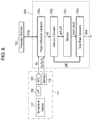
- FIG. 3 is a block diagram of a drive circuit of the physical quantity sensor according to Embodiment 1.
- FIG. 4 illustrates phase characteristics of an oscillator of the physical quantity sensor according to Embodiment 1.
- FIG. 5A illustrates a phase difference measurement method by a phase difference detector of the physical quantity sensor according to Embodiment 1.
- FIG. 5B is an enlarged view of FIG. 5A .
- FIG. 6 illustrates a phase difference in the physical quantity sensor according to Embodiment 1.
- FIG. 7 is a block diagram of a sine-wave generating unit of the physical quantity sensor according to Embodiment 1.
- FIG. 8 is a block diagram of another sine-wave generating unit of the physical quantity sensor according to Embodiment 1.
- FIG. 9 is a block diagram of another physical quantity sensor according to Embodiment 1.
- FIG. 10 is a block diagram of still another physical quantity sensor according to Embodiment 1.
- FIG. 11 is a block diagram of a further physical quantity sensor according to Embodiment 1.
- FIG. 12 is a schematic diagram of an electronic device according to Embodiment 1.
- FIG. 13 is a block diagram of an amplifier circuit according to Exemplary Embodiment 2.
- FIG. 14 is a block diagram of another amplifier circuit according to the second exemplary embodiment.
- FIG. 15 illustrates output characteristics of the amplifier circuit according to Embodiment 2.
- FIG. 16 is a schematic diagram of a physical quantity sensor according to Exemplary Embodiment 3.
- FIG. 17 is a block diagram of a drive circuit according to Exemplary Embodiment 4.
- FIG. 18 is a block diagram of another drive circuit according to Embodiment 4.
- FIG. 1 is a schematic diagram of physical quantity sensor 1 according to Exemplary Embodiment 1.
- Physical quantity sensor 1 includes oscillator 10 , drive circuit 11 , and physical-quantity detecting circuit 51 .
- Drive circuit 11 supplies drive signal Sdrv having predetermined drive frequency fdrv to oscillator 10 .
- Oscillator 10 outputs sensor signals S 10 a and S 10 b according to physical quantities, such as an angular velocity or acceleration, supplied from outside.
- the frequency of sensor signals S 10 a and S 10 b corresponds to frequency fdrv of drive signal Sdrv.
- the center frequency of sensor signals S 10 a and S 10 b corresponds to frequency fdrv of drive signal Sdrv, and is substantially identical to frequency fdrv.
- oscillator 10 is a tuning fork-type angular velocity sensor that outputs sensor signals S 10 a and S 10 b according to an angular velocity, a physical quantity, supplied from outside.
- Drive circuit 11 supplies drive signal Sdrv to oscillator 10 .
- Oscillator 10 vibrates due to drive signal Sdrv, and outputs monitor signal Sosc according to the vibration.
- Drive circuit 11 adjusts frequency fdrv and amplitude Adrv of drive signal Sdrv according to monitor signal Sosc from oscillator 10 .
- Physical-quantity detecting circuit 51 detects a physical quantity applied to the oscillator based on sensor signals S 10 a and S 10 b from oscillator 10 .
- FIG. 2 is a block diagram of physical quantity sensor 1 .
- Oscillator 10 has oscillator body 10 a having a tuning fork shape, driving piezoelectric element Pdrv, oscillation-detecting piezoelectric element Posc, and physical-quantity-detecting piezoelectric elements PDa and PDb.
- Driving piezoelectric element Pdrv drives oscillator body 10 a to vibrate oscillator body 10 a according to frequency fdrv and amplitude Adrv of drive signal Sdrv from drive circuit 11 . This vibration causes oscillation-detecting piezoelectric element Posc to generate electric charges and produce monitor signal Sosc, a current of the flow of the electric charges.
- FIG. 3 is a block diagram of drive circuit 11 .
- IV converter 13 converts monitor signal Sosc, the electric current output from oscillator 10 , to monitor signal Vosc, a voltage.
- Analog-digital converter (ADC) 15 converts monitor signal Vosc output from IV converter 13 into digital values, monitor signal Dosc.
- a filter such as a low-pass filter (LPF) or a band-pass filter (BPF), may be connected either upstream or downstream, or both upstream and downstream of ADC 15 .
- LPF low-pass filter
- BPF band-pass filter
- a BPF is provided at each of both upstream and downstream of ADC 15 .
- Phase difference detector 17 receives monitor signal Dosc output from ADC 15 and drive signal Qdrv having a digital value along a sine wave generated in drive signal generating unit 21 . By performing an arithmetic operation to monitor signal Dosc and drive signal Qdrv generated by drive signal generating unit 21 , phase difference detector 17 calculates phase difference information Dpd according to phase difference Pd between monitor signal Dosc and drive signal Qdrv, and outputs phase difference information Dpd to frequency controller 19 .
- Frequency controller 19 calculates phase step value Pst that determines drive frequency fdrv of drive signal Sdrv based on phase difference information Dpd supplied from phase difference detector 17 , and outputs phase step value Pst to drive signal generating unit 21 .
- Drive signal generating unit 21 generates drive signal Qdrv, a digital value of a sine wave, based on phase step value Pst obtained from frequency controller 19 , and outputs drive signal Qdrv to automatic gain control (AGC) unit 23 .
- Drive signal generating unit 21 includes phase calculator 21 a and sine-wave generator 21 b .
- Phase calculator 21 a outputs phase information Pss ranging from 0 to 2 ⁇ according to phase step value Pst.
- Phase calculator 21 a cumulates phase step values Pst obtained from frequency controller 19 at predetermined constant time intervals to obtain a cumulative value, and calculates a remainder as phase information Pss obtained by dividing the cumulative value by 2 ⁇ .
- Phase calculator 21 a may obtain a subtraction value by subtracting 2 ⁇ from the cumulative value one or more times until the subtraction value falls within the range equal to or larger than 0 and smaller than 2 ⁇ , and then employ the subtraction value as phase information Pss.
- Sine-wave generator 21 b includes, for example, a CORDIC arithmetic circuit, and generates drive signal Qdrv having a difital value of a sine wave by calculating amplitude information corresponding to phase information Pss.
- AGC unit 23 includes amplitude detector 23 a , gain controller 23 b , and multiplier 23 c.
- Amplitude detector 23 a detects amplitude Damp of monitor signal Dosc.
- Multiplier 23 c multiplies gain value Gc calculated by gain controller 23 b by drive signal Qdrv generated by drive signal generating unit 21 so as to generate drive signal Ddrv, which is a gain-controlled digital value, and outputs drive signal Qdrv to output unit 11 p .
- Output unit 11 p includes digital-analog converter (DAC) 25 which receives drive signal Ddrv.
- DAC 25 converts drive signal Ddrv into drive signal Sdrv which is an analog signal, and outputs drive signal Sdrv to oscillator 10 .
- Output unit 11 p may include a LPF or a BPF connected downstream of DAC 25 . This configuration preferably provides high SN ratio.
- Embodiment 1 performs frequency control with phase characteristics of oscillator 10 . This operation will be detained below.
- FIG. 4 illustrates phase characteristics of oscillator 10 .
- Oscillator 10 has resonance frequency f0.
- the phase of the vibration of oscillator 10 advances when the phase changes in a positive (+) direction with respect to resonance frequency f0.
- the phase of the vibration of oscillator 10 delays when the phase changes in a negative ( ⁇ ) direction.
- the frequency of drive signal Qdrv is higher than resonance frequency f0, the phase changes in the positive direction and advances.
- the frequency of drive signal Qdrv is lower than resonance frequency f0, the phase changes in the negative direction and delays.
- FIG. 5A illustrates a method of measuring phase difference Pd by phase difference detector 17 .
- the horizontal axis represents time
- the vertical axis represents values of drive signal Qdrv and monitor signal Dosc.
- Drive signal Qdrv takes value Qdrv(tN) at sampling point tN (where N is an integer).
- N is an integer.
- Each of the values of drive signal Qdrv and monitor signal Dosc changes within a width of the amplitude from zero at the center of the width, and repetitively takes a positive value and a negative value alternately.
- phase difference Pd between monitor signal Dosc and drive signal Qdrv In order to measure phase difference Pd between monitor signal Dosc and drive signal Qdrv accurately, the phase difference is measured at zero-crossing points where monitor signal Dosc and drive signal Qdrv cross the zero point, not around vertices of monitor signal Dosc and drive signal Qdrv.
- the amount of change of the signal is larger around the zero-crossing point than around the vertex, hence decreasing the measurement error of a signal level and a calculation error in calculating the phase difference.
- ADC 15 and sections that process digital signals operate based on a sampling clock having a predetermined sampling period Ts.
- Phase difference detector 17 samples drive signal Qdrv and monitor signal Dosc at sampling points t 0 , t 1 , . . . at time intervals of sampling period Ts.
- Phase difference detector 17 according to Embodiment 1 detects zero-crossing points tzd 1 and tzd 2 of drive signal Qdrv and zero-crossing point tzm 1 of monitor signal Dosc.
- zero-crossing points tzd 1 and tzd 2 of drive signal Qdrv are time points at which the value of drive signal Qdrv crosses the zero value while changing from a negative value to a positive value.
- Zero-crossing point tzm 1 of monitor signal Dosc is a time point at which the value of monitor signal Dosc crosses the zero value while changing from a negative value to a positive value.
- the zero value of drive signal Qdrv and the zero value of monitor signal Dosc are center value Zdrv of drive signal Qdrv and center value Zosc of monitor signal Dosc, respectively.
- zero-crossing points tzd 1 and tzd 2 of drive signal Qdrv are the time points at which the value of drive signal Qdrv crosses center value Zdrv of drive signal Qdrv in a rising direction in which drive signal Qdrv increases.
- Zero-crossing point tzm 1 of monitor signal Dosc is the time point at which the value of monitor signal Dosc crosses center value Zosc of monitor signal Dosc in a rising direction in which monitor signal Dosc increases.
- zero-crossing point tzd 2 of drive signal Qdrv is the next zero-crossing point of zero-crossing point tzd 1 of drive signal Qdrv, that is, the zero-crossing point firstly appearing subsequent to zero-crossing point tzd 1 of drive signal Qdrv.
- Zero-crossing point tzm 1 of monitor signal Dosc is the zero-crossing point firstly appearing subsequent to zero-crossing point tzd 1 of drive signal Qdrv.
- Zero-crossing point tzd 2 of drive signal Qdrv is the zero-crossing point firstly appearing subsequent to zero-crossing point tzm 1 of monitor signal Dosc.
- Drive signal Qdrv and monitor signal Dosc may cross the center values in a falling direction at zero-crossing points.
- the value of drive signal Qdrv may cross center value Zdrv in a falling direction in which drive signal Qdrv changes from a positive value to a negative value.
- the value of monitor signal Dosc crosses center value Zosc in a falling direction in which monitor signal Dosc changes from a positive value to a negative value.
- Phase difference detector 17 calculates phase difference Pd with period Tdrv of drive signal Qdrv and time difference Tdm from zero-crossing point tzd 1 of drive signal Qdrv to zero-crossing point tzm 1 of monitor signal Dosc according to Formula 1.
- Phase difference detector 17 obtains period Tdrv of drive signal Qdrv as follows.
- Phase difference detector 17 obtains fractional part Fr1 which is a duration from zero-crossing point tzd 1 of drive signal Qdrv to the first sampling point t 1 subsequent to zero-crossing point tzd 1 .
- Phase difference detector 17 measures integer part In1 which is a duration that can be counted by the sampling clock from sampling point t 1 to sampling point t 16 immediately before zero-crossing point tzd 2 of drive signal Qdrv.
- Phase difference detector 17 obtains fractional part Fr2 which is a duration from sampling point t 16 to zero-crossing point tzd 2 of drive signal Qdrv.
- Phase difference detector 17 obtains period Tdrv of drive signal Qdrv according to Formula 2.
- Tdm Fr 1+ In 2+ Fr 3 [Formula 2]
- Phase difference detector 17 obtains time difference Tdm between zero-crossing point tzd 1 of drive signal Qdrv and zero-crossing point tzm 1 of monitor signal Dosc as follows.
- Phase difference detector 17 measures integer part In2 which is a duration that can be counted by the sampling clock from sampling point t 1 to sampling point t 11 immediately before zero-crossing point tzm 1 of monitor signal.
- Phase difference detector 17 obtains fractional part Fr3 which is a duration from sampling point t 11 to zero-crossing point tzm 1 of monitor signal Dosc.
- Phase difference detector 17 obtains time difference Tdm between zero-crossing point tzd 1 of drive signal Qdrv and zero-crossing point tzm 1 of monitor signal Dosc according to Formula 3.
- Tdm Fr 1+ In 2+ Fr 3 [Formula 3]
- FIG. 5B illustrates a method for phase difference detector 17 to measure fractional part Fr1, and shows a region around zero-crossing point tzd 1 shown in FIG. 5A whle enlarging the region.
- Phase difference detector 17 obtains fractional part Fr1 with value Qdrv(t 0 ) of drive signal Qdrv at sampling point t 0 immediately before zero-crossing point tzd 1 and value Qdrv(t 1 ) of drive signal Qdrv at sampling point t 1 subsequent to sampling point t 0 , that is, at sampling point t 1 immediately subsequent to zero-crossing point tzd 1 according to Formula 4.
- phase difference detector 17 obtains fractional part Fr2 with value Qdrv(t 16 ) of drive signal Qdrv at sampling point t 16 immediately before zero-crossing point tzd 2 and value Qdrv(t 17 ) of drive signal Qdrv at sampling point t 17 subsequent to sampling point t 16 , that is, at sampling point t 17 immediately subsequent to zero-crossing point tzd 2 according to Formula 5.
- phase difference detector 17 obtains fractional part Fr3 with value Qdrv(t 11 ) of drive signal Qdrv at sampling point t 11 immediately before zero-crossing point tzm 1 and value Qdrv(t 12 ) of drive signal Qdrv at sampling point t 12 subsequent to sampling point t 11 , that is, at sampling point t 12 immediately subsequent to zero-crossing point tzm 1 according to Formula 6.
- Phase difference detector 17 outputs phase difference information Dpd according to phase differences Pd calculated by Formulae 1 to 6.
- frequency controller 19 An operation of frequency controller 19 will be described below.
- FIG. 6 illustrates phase difference Pd between monitor signal Dosc and drive signal Qdrv.
- phase difference Pd when drive frequency fdrv shifts from resonance frequency f0 of oscillator 10 , phase difference Pd between drive signal Qdrv and monitor signal Dosc converges toward the phase difference shown in FIG. 4 over time. But until the convergence, phase difference Pd changes over time as shown in FIG. 6 depending on the difference between drive frequency fdrv and resonance frequency f0. Thus, the gradients of the phase changes over time change depending on the amount of the shift of frequency. Specifically, when resonance frequency f0 is higher than drive frequency fdrv, phase difference Pd converges over time to positive value Pd1 according to property P1. When resonance frequency f0 is lower than drive frequency fdrv, phase difference Pd converges over time to negative value Pd2 according to property P2.
- the drive circuit of the physical quantity sensor disclosed in PTL 1 performs a band-pass filter (BPF) process and an automatic gain control (AGC) process on the monitor signal of the oscillator, and outputs the processed signal as a drive signal.
- BPF band-pass filter
- AGC automatic gain control
- the monitor signal contains unnecessary components
- the drive signal also contain the unnecessary components, consequently preventing the drive circuit to cause stable driving and oscillation.
- Drive circuit 11 roughly tunes drive frequency fdrv to resonance frequency f0 of oscillator 10 first at a startup mode.
- the startup mode reduces the time until the convergence in the case that drive frequency fdrv at an initial start stage is drastically different from resonance frequency f0 of oscillator 10 .
- a large error may occur since the amplitude of monitor signal Dosc is small in a duration at the initial stage.
- monitor signal Dosc in this duration is not used to control frequency fdrv, thereby allowing frequency fdrv to be controlled stably.
- the operation is performed with predetermined initial value Psti of phase step value Pst and predetermined initial value Gci of gain value Gc for predetermined duration Ti in the starting during which the output from oscillator 10 is not generated upon being turned on.
- Drive signal Sdrv having a fixed amplitude based on predetermined initial value Gci of gain value Gc and a fixed frequency based in predetermined initial value Psti of phase step value Pst is output to oscillator 10 for predetermined duration Ti.
- Initial value Psti and initial value Gci as well as predetermined duration Ti is preferably stored in, e.g. a memory.
- frequency controller 19 calculates phase step value Pst based on the measured phase at the time point when predetermined duration Ti elapses.
- Frequency controller 19 calculates phase step value Pst(m) at time point t(m) with phase difference Pd(m) at time point t(m), step value Pst(m ⁇ 1) at time point t(m ⁇ 1) immediately before time point t(m), and frequency control factor K1 at the time of starting (wherein m is an integer) according to Formula 7.
- timer with predetermined duration Ti is operated at the time of starting, and drive frequency fdrv is controlled by frequency controller 19 based on phase difference Pd that has been calculated at the time point when predetermined duration Ti elapses.
- Pst ( m ) Pst ( m ⁇ 1)+ K 1 ⁇ Pd ( m ) [Formula 7]
- frequency controller 19 controls drive frequency fdrv by a proportional-derivative (PD) control.
- Frequency controller 19 obtains phase step value Pst(m) at time point t(m), with using phase difference Pd(m) at time point t(m), phase step value Pst(m ⁇ 1) at time point t(m ⁇ 1) immediately before time point t(m), phase difference Pd(m ⁇ 1), P-component Kp of the frequency control factor in a steady state, and D-component Kd of the frequency control factor in a steady state according to Formula 8.
- Pst ( m ) Pst ( m ⁇ 1)+ Kp ⁇ Pd ( m )+ Kd ⁇ ( Pst ( m ) ⁇ Pst ( m ⁇ 1)) [Formula 8]
- P-component Kp is a proportional gain for controlling the manipulated variable as a linear function of a control valuable and a deviation from a target value.
- D-component Kd is a differential gain for controlling an input value proportional to the differential of phase difference Pd.
- This control may be proportional (P) control or proportional-integral-derivative (PID) control, depending on the target control characteristics.
- This operation allows drive frequency fdrv to be equal to resonance frequency f0 of oscillator 10 based on phase difference Pd.
- AGC unit 23 performs a control operation, for example, by proportional control as described below.
- Frequency fdrv of drive signal Qdrv (drive signal Ddrv) is controlled by detecting a difference between frequency fdrv of drive signal Qdrv and resonance frequency f0 based on phase difference Pd, and the amplitude of drive signal Ddrv is controlled by AGC control by detecting amplitude Aosc of monitor signal Dosc, as described above.
- This configuration drives oscillator 10 to vibrate oscillator 10 stably, providing precise physical quantity sensor 1 .
- ADC 15 , phase difference detector 17 , and AGC unit 23 may stop or may be intermittently driven. This configuration increases the period of control and reduces power consumption.
- Physical-quantity detecting circuit 51 will be described below.
- physical-quantity detecting circuit 51 includes waveform shaping unit 101 , frequency multiplier 102 , detection-signal generating unit 100 , input amplifier 103 , analog-digital converter (ADC) 105 , multiplier 115 , and digital filter 120 .
- waveform shaping unit 101 frequency multiplier 102
- detection-signal generating unit 100 input amplifier 103
- ADC analog-digital converter
- Waveform shaping unit 101 converts monitor signal Sosc to a rectangular wave and outputs the rectangular wave as reference clock CKref.
- waveform shaping unit 101 is implemented by a comparator or an inverter.
- the frequency of reference clock CKref is identical to the frequency of sensor signals S 10 a and S 10 b .
- reference clock CKref is substantially identical to frequency fdrv of drive signal Sdrv.
- Frequency multiplier 102 multiplies the frequency of reference clock CKref from waveform shaping unit 101 and generates frequency-multiplied clock CKsp having a frequency higher than the frequency of reference clock CKref.
- frequency multiplier 102 is implemented by a phase locked loop (PLL).
- Input amplifier 103 converts sensor signals S 10 a and S 10 b , currents from oscillator 10 , into voltages, and outputs the voltages as analog sensor signal Asnc.
- Mechanical coupling canceller (MCC) 104 superimposes a MC signal obtained by adjusting the phase of drive signal Sdrv on analog sensor signal Asnc. This operation cancels at least a portion of an unnecessary signal, a signal unnecessary to detect the physical quantity, contained in analog sensor signal Asnc.
- Analog-digital converter 105 samples analog sensor signal Asnc in synchronization with sampling clock CKsp and converts the sampled analog values (amplitude values) into digital values, digital sensor signal Dsnc. Analog sensor signal Asnc is thus converted into digital sensor signal Dsnc composed of plural digital values.
- Detection-signal generating unit 100 includes sine-wave generating unit 106 , temperature detector 107 , low-pass filter (LPF) 108 , analog-digital converter (ADC) 109 , and memory 110 .
- LPF low-pass filter
- ADC analog-digital converter
- Temperature information corresponds to a temperature obtained by temperature detector 107 is filtered by low-pass filter 108 , and is converted into digital values, temperature information Dt, by analog-digital converter 109 .
- the converted temperature information Dt is input into sine-wave generating unit 106 at a predetermined period.
- Memory 110 stores plural values of correction amount Ea, plural values of correction amount Eb, and plural values of correction amount Ec which correspond to plural values of temperature information Dt.
- Temperature detector 107 , low-pass filter 108 , analog-digital converter 109 , and memory 110 constitute correction amount generating unit 111 .
- FIG. 7 is a block diagram of sine-wave generating unit 106 .
- Sine-wave generating unit 106 includes phase calculator 106 a and sine-wave generator 106 d , and is connected to correction amount generating unit 111 .
- Phase calculator 106 a calculates phase ⁇ 1 based on frequency-multiplied clock CKsp obtained from frequency multiplier 102 .
- Phase calculator 106 a also obtains, from memory 110 , the values of correction amounts Ea, Eb, and Ec corresponding to temperature information Dt obtained by temperature detector 107 , and converts phase ⁇ 1 to calculate phase ⁇ 2 based on the obtained values of correction amounts Ea, Eb, and Ec.
- phase ⁇ 2 can be calculated according to Formula 10.
- ⁇ 2 ⁇ 1+ Ea ⁇ Dt 2 +Eb ⁇ Dt+Ec [Formula 10]
- Sine-wave generator 106 d generates detection signal Ddet, which is a sine wave, by calculating the amplitude value corresponding to phase ⁇ 2, which is input from phase calculator 106 a .
- a CORDIC computation for example, may be used as the computational method for generating a sine wave by feeding a certain phase.
- FIG. 8 is a block diagram of another sine-wave generating unit 606 according to Embodiment 1.
- components identical to those of sine-wave generating unit 106 shown in FIG. 7 are dented by the same reference numerals.
- Sine-wave generating unit 606 includes phase calculator 106 a , address calculator 106 b , memory 106 c , and sine-wave generator 106 d.
- Phase calculator 106 a calculates phase ⁇ 1 based on frequency-multiplied clock CKsp obtained from frequency multiplier 102 .
- Phase calculator 106 a obtains, from memory 110 , the values of correction amounts Ea, Eb, and Ec corresponding to temperature information Dt obtained by temperature detector 107 and calculates phase ⁇ 2 by converting phase ⁇ 1 to phase ⁇ 2 based on the acquired values of correction amounts Ea, Eb, and Ec. Then, calculated phase ⁇ 2 is output to address calculator 106 b.
- Address calculator 106 b stores addresses corresponding to plural values of phase ⁇ 2 .
- Table 1 shows the values of phase ⁇ 2 and the addresses corresponding to the values of phase ⁇ 2 which are stored in address calculator 106 b .
- Address calculator 106 b an address out of the plural addresses which corresponds to phase ⁇ 2 input from phase calculator 106 a , and outputs the selected address to memory 106 c . More specifically, address calculator 106 b selects address ad1 corresponding to a stored value out of the stored values of phase ⁇ 2 which is closest to the input value of phase ⁇ 2 and smaller than the input value of phase ⁇ 2, and selects address ad2 corresponding to a stored value out of the stored values of phase ⁇ 2 which is closest to the input value of phase ⁇ 2 and larger than the input value of phase ⁇ 2. Address calculator 106 b outputs addresses ad1 and ad2 to memory 106 c .
- address calculator 106 b selects address “2”, which corresponds to 0.049 (rad) which a stored value out of the stored values which is closest to 0.06 (rad) and smaller than 0.06 (rad), and selects address “3”, which corresponds to 0.074 which is a stored value out of the stored values which is closest to 0.06 (rad) and larger than 0.06 (rad).
- Address calculator 106 b outputs the selected addresses “2” and “3” to memory 106 c .
- Address calculator 106 b outputs addresses ad1 and ad2 to memory 106 c .
- Address calculator 106 b calculates address ad0 corresponding to phase ⁇ 2 with phase step Ps obtained by dividing 2 ⁇ by the number of the addresses according to the following formula, and outputs address ad0 to sine-wave generator 106 d.
- ad 0 ⁇ 2 ⁇ (1/ Ps )
- Memory 106 c stores plural addresses and plural amplitude values corresponding to the addresses.
- Table 2 shows addresses and amplitude values stored in memory 106 c .
- Memory 106 c outputs, to sine-wave generator 106 d , amplitude values data1 and data 2 corresponding to addresses ad1 and ad2, respectively, that are input from address calculator 106 b .
- memory 106 c outputs, to sine-wave generator 106 d , an amplitude value “0.0049 (0.004907)” corresponding to address “2”, and outputs, to sine-wave generator 106 d , an amplitude value “0.0073 (0.007356)” corresponding to address “3”.
- Sine-wave generator 106 d generates detection signal Ddet which is a sine wave using addresses ad0, ad1, and ad2 and amplitude values data1 and data 2 according to the following formula.
- Ddet data1+( ad 0 ⁇ ad 1) ⁇ (data2 ⁇ data1)
- Multiplier 115 multiplies digital sensor signal Dsnc from analog-digital converter 105 by detection signal Ddet generated by sine-wave generating unit 106 . Multiplier 115 thereby detects physical quantity signal D 115 which corresponds to the physical quantity detected by oscillator 10 .
- digital filter 120 passes only low frequency components of physical quantity signal D 115 detected by multiplier 115 as digital detected signal Dphy.
- the above-described configuration can calculate a sine wave signal with arbitrary phase by an arithmetic operation.
- This provides high precision adjustment of detection phase that cannot be achieved by analog-like adjustment or adjustment of detection signal or physical quantity signal in an actual time direction such as to be dependent on clock signal, through the arithmetic operation without increasing the clock frequency.
- environment parameters such as a temperature
- detection can be carried out by using a sine wave signal with an appropriately adjusted phase as a detection signal and multiplying the detection signal by a signal to be detected, thus providing precise and low-cost physical quantity sensor 1 without increasing power consumption and circuit scale.
- Oscillator 10 according to the Embodiment 1 may not necessarily have a tuning fork shape, but may have another shape, such as a circular column shape, a right triangular column shape, a right quadrangular column shape, or a ring shape.
- FIG. 9 is a block diagram of another physical quantity sensor 601 according to Embodiment 1.
- Physical quantity sensor 601 shown in FIG. 9 includes oscillator 610 which is a capacitance-type acceleration sensor instead of oscillator 10 of physical quantity sensor 1 shown in FIGS. 1 and 2 .
- Oscillator 610 includes stationary portion 10 b , movable portion 10 c , movable electrodes Pma and Pmb, detection electrodes Pfa and Pfb, and differential amplifier 10 d .
- Movable portion 10 c is coupled to stationary portion 10 b and is displaced according to acceleration.
- Movable electrodes Pma and Pmb are disposed on movable portion 10 c .
- Detection electrodes Pfa and Pfb are disposed on stationary portion 10 b and face movable electrodes Pma and Pmb, respectively.
- Movable electrode Pma and detection electrode Pfa constitute capacitor element Ca while movable electrode Pmb and detection electrode Pfb constitute capacitor element Cb.
- Drive signal Sdrv is supplied to capacitor elements Ca and Cb from drive circuit 11 .
- Differential amplifier 10 d outputs sensor signals S 10 a and S 10 b corresponding to a difference between charge amounts produced in detection electrodes Pfa and Pfb.
- Acceleration applied to movable portion 10 c displaces movable portion 10 c , hence increasing one of the capacitances of capacitor elements Ca and Cb and decreasing the other of the capacitances of capacitor elements Ca and Cb decreases. This causes a difference between the amounts of charges on detection electrodes Pfa and Pfb.
- the detection electrodes outputs sensor signals S 10 a and S 10 b corresponding to the difference.
- FIG. 10 is a block diagram of still another physical quantity sensor 701 according to Embodiment 1.
- Physical quantity sensor 701 shown in FIG. 10 includes oscillator 710 , a capacitance-type angular velocity sensor, instead of oscillator 610 of physical quantity sensor 601 shown in FIG. 9 .
- Drive signal Sdrv is supplied to oscillator 710 from drive circuit 11 to drive movable portion 10 c to vibrate movable portion 10 c .
- Rotation applied to oscillator 10 while vibrating allows movable portion 10 c to cause detection oscillation according to the Coriolis force due to the rotation.
- the detection oscillation increases one of the capacitances of capacitor elements Ca and Cb, and decreases the other of the capacitances of capacitor elements Ca and Cb. This causes a difference between the amounts of charges on detection electrodes Pfa and Pfb.
- the detection electrodes output sensor signals S 10 a and S 10 b corresponding to the difference.
- FIG. 11 is a block diagram of further physical quantity sensor 801 according to Embodiment 1.
- Physical quantity sensor 801 further includes down-sampling processor 105 a (decimation filter) connected downstream of AD converter 105 .
- Down-sampling processor 105 a thins out digital values from digital sensor signal Dsnc.
- Down-sampling processor 105 a thins out digital sensor signal Dsnc to reduce the sampling frequency of digital sensor signal Dsnc and reduce the sampling frequency of digital physical quantity signal D 115 supplied to digital filter 120 . This configuration can reduce the circuit scale and power consumption of digital filter 120 .
- band-pass filter 15 a may be connected between ADC 15 and AGC unit 23 of drive circuit 11 .
- Monitor signal Sosc input to waveform shaping unit 101 shown in FIG. 1 may be obtained either from the upstream or downstream of band-pass filter 15 a.
- FIG. 12 is a block diagram of electronic device 70 including physical quantity sensor 1 according to Embodiment 1.
- Electronic device 70 may be, for example, a digital camera, and includes physical quantity sensor 1 , display 71 , processor 72 , such as CPU, memory 73 , and operating unit 74 .
- Physical quantity sensor 1 is an angular velocity sensor. As illustrated in, e.g. FIG. 1 , physical quantity sensor 1 includes oscillator 10 , drive circuit 11 , and physical-quantity detecting circuit 51 .
- Physical quantity sensor 1 has a small size, small power consumption, and high precision. Therefore, in the case that electronic device 70 is a video camera or a digital still camera, electronic device 70 including physical quantity sensor 1 can have s small size, small power consumption, and precise processing, such as image stabilization.
- Physical quantity sensor 1 provides electronic device 70 with high performance. Besides the digital cameras, electronic device 70 may be an automobile navigation system, a vehicle, an aircraft, or a robot.
- drive circuit 11 is configured to drive oscillator 10 to vibrate oscillator 10 .
- Oscillator 10 outputs monitor signal Sosc according to a physical quantity.
- Drive circuit 11 includes drive signal generating unit 21 generating drive signal Qdrv having drive frequency fdrv, phase difference detector 17 detecting phase difference Pd between monitor signal Dosc and drive signal Qdrv, frequency controller 19 controlling drive frequency fdrv based on phase difference Pd, AGC unit 23 controlling an amplitude of drive signal Ddrv according to an amplitude of monitor signal Dosc, output unit 11 p outputting drive signal Sdrv having the controlled amplitude to oscillator 10 .
- Frequency controller 19 may detect a difference between drive frequency fdrv and resonance frequency f0 of oscillator 10 based on phase difference Pd so as to control drive frequency fdrv.
- Output unit 11 p may output a sine wave signal having a predetermined frequency and a predetermined amplitude to oscillator 10 when starting oscillator 10 .
- drive circuit 11 may detect the amplitude of monitor signal Sosc and may be switched to control drive signal Sdrv by AGC.
- One of analog-digital converter unit 15 , phase difference detector 17 , and AGC unit 23 may operate intermittently.
- Phase difference detector 17 may obtain phase difference Pd based on time difference Tdm between drive signal Qdrv and monitor signal Dosc and period Tdrv of drive signal Qdrv according to the following formula:
- Phase difference detector 17 may be configured to sample drive signal Qdrv at sampling point t 1 immediately subsequent to zero-crossing point tzd 1 with a sampling clock. In this case, phase difference detector 17 is configured to sample drive signal Qdrv at sampling point t 16 immediately before zero-crossing point tzd 2 with the sampling clock.
- Monitor signal Dosc crosses center value Zosc of monitor signal Dosc at zero-crossing point tzm 1 subsequent to sampling point t 1 in the predetermined direction.
- Phase difference detector 17 may be configured to sample monitor signal Dosc from sampling point t 1 to sampling point t 11 immediately before zero-crossing point tzm 1 with the sampling clock.
- Phase difference detector 17 may start detecting phase difference Pd after a predetermined duration elapses after the starting of oscillator 10 .
- the frequency controller may control drive frequency fdrv by PD control in a steady state of oscillator 10 .
- FIG. 13 is a block diagram of amplifier circuit 200 according to Exemplary Embodiment 2.
- Amplifier circuit 200 includes input ports 212 and 214 , transistor 216 connected to input port 212 , transistor 218 connected input port 214 , current amplifier 220 connected to an output port of transistor 216 and an output port of transistor 218 , current source 222 connected between transistor 216 and current amplifier 220 , and output port 224 .
- Input port 212 is a part to which an electric signal is input from outside.
- Input port 212 may not necessarily be a physical terminal but may be any part to which an electric signal is input from outside.
- Input port 214 is a part to which an electric signal is input from outside.
- Input port 214 may not necessarily be a physical terminal but may be any part to which an electric signal is input from outside.
- Transistor 216 is connected to input port 212 .
- An output port of transistor 216 is connected to a primary side of current amplifier 220 .
- Transistor 218 is connected to input port 214 .
- An output port of transistor 218 is connected to the primary side of current amplifier 220 .
- an output port of transistor 218 is connected between the output port of transistor 216 and the primary side of current amplifier 220 .
- Current source 222 is connected between the output port of transistor 216 and the primary side of current amplifier 220 .
- Output port 224 is connected to a secondary side of current amplifier 220 , and is a part that outputs an electric signal to outside.
- Output port 224 may not necessarily be a physical terminal, but may be any part that outputs an electric signal to outside.
- amplifier circuit 200 An operation of amplifier circuit 200 will be described below.
- Output port 224 i.e., an output of amplifier circuit 200 becomes out of a limited range
- transistor 216 has high impedance. This reduces the signal current output from transistor 216 .
- transistor 218 has low impedance, and a current output from transistor 218 increases.
- the current flowing through the primary side of current amplifier 220 is almost controlled by the output current of transistor 218 .
- the current flowing through the secondary side of current amplifier 220 is also controlled, so that the output from output 224 , i.e., the output of amplifier circuit 200 , is controlled to a value input from input port 214 .
- potential Vcc connected to the sources or emitters of transistors 216 and 218 and current amplifier 220 is at a high potential while potential Vdd connected to current source 222 is at a low potential lower than potential Vcc.
- potential Vcc connected to the sources or emitters of transistors 216 and 218 and current amplifier 220 is at a low potential while potential Vdd connected to current source 222 is at a high potential higher than potential Vcc.
- a power source used for supplying the high potential may preferably be, for example, a stabilized power supply, such as power supply voltage.
- a power source used for supplying the low potential may preferably be, for example, a ground potential.
- the high and low potentials may also be connected via resistors.
- FIG. 14 is a block diagram of another amplifier circuit 201 according to Embodiment 2.
- Amplifier circuit 201 includes amplifier 242 having differential output ports, amplifier 244 , amplifier 246 , transistor 216 connected to one of the output ports of amplifier 242 , transistor 218 connected to an output port of amplifier 244 , current source 222 connected to an output port of transistor 216 and an output port of transistor 218 , current amplifier 220 connected to the output port of transistor 216 and the output port of transistor 218 , transistor 266 connected to the other output port of amplifier 242 , transistor 268 connected to an output port of amplifier 246 , current source 272 connected to an output port of transistor 266 and an output port of transistor 268 , current amplifier 270 connected to the output port of transistor 266 and the output port of transistor 268 , and an output circuit 280 for providing a push-pull control output signal, connected to output ports of current amplifiers 220 and 270 .
- Current amplifier 220 has a primary side terminal and a secondary side terminal.
- the output port of transistor 216 and the output port of transistor 218 are connected to the primary side terminal of current amplifier 220 .
- Current amplifier 270 has a primary side and a secondary side.
- the output port of transistor 266 and the output port of transistor 268 are connected to the primary side terminal of current amplifier 270 .
- potential Vcc connected to the sources or emitters of transistors 216 and 218 and current amplifier 220 is at a high potential while potential Vdd connected to current source 222 is at a low potential lower than potential Vcc.
- potential Vcc connected to the sources or emitters of transistors 266 and 268 and current amplifier 270 is at a high potential while potential Vdd connected to current source 272 is at a low potential lower than potential Vcc.
- potential Vcc connected to the sources or emitters of transistors 216 and 218 and current amplifier 220 is at a low potential while potential Vdd connected to current source 222 is at a high potential higher than potential Vcc.
- potential Vcc connected to the sources or emitters of transistors 266 and 268 and current amplifier 270 is at a low potential while potential Vdd connected to current source 272 is at a high potential higher than potential Vcc.
- a power source used for supplying the high potential may preferably be, for example, a stabilized power supply, such as power supply voltage.
- a power source used for supplying the low potential may preferably be, for example, a ground potential.
- the high and low potentials may also be connected via resistors.
- FIG. 15 illustrates output signals with respect to input signals in the case that the output port of amplifier circuit 201 constitutes a negative feedback connection.
- FIG. 15 shows limited range R 201 of the output of amplifier circuit 201 , upper limit L 201 of limited range R 201 , and lower limit L 202 of limited range R 201 .
- the output signal exceeding upper limit L 201 is indicated by the dotted line at a position higher than upper limit L 201 .
- the output signal below lower limit L 202 is indicated by the dotted line at a position lower than lower limit L 202 .
- transistors 216 and 266 When the output signal is within limited range R 201 , transistors 216 and 266 receive differential outputs of amplifier 242 to differentially operate, thereby controlling a outflowing current and a lead-in current of output circuit 280 . The output signal is thus output.
- transistor 216 When the output signal increases beyond upper limit L 201 of limited range R 201 , transistor 216 has high impedance while transistor 218 has low impedance due to a controlled by the output of amplifier 244 . Thus, the current flowing through the primary side of current amplifier 220 is almost controlled by transistor 218 .
- Voltage V 244 for setting upper limit L 201 is input to one of the input ports of amplifier 244 .
- An output signal of output circuit 280 is fed back to the other input port of amplifier 244 .
- Transistor 218 is connected to the output port of amplifier 244 .
- the output port of amplifier 244 is substantially fixed to a potential substantially equal to upper limit L 201 .
- transistor 266 When the output signal decrease below lower limit L 202 of limited range R 201 , transistor 266 has high impedance while transistor 268 has low impedance due to a control by the output of amplifier 246 . Thus, the current flowing through the primary side of current amplifier 270 is almost controlled by transistor 268 .
- Voltage V 246 for setting lower limit L 202 is input to one of the input ports of amplifier 246 .
- An output signal of output circuit 280 is fed back to the other input port of amplifier 246 .
- Transistor 268 is connected to the output port of amplifier 246 .
- the output port of amplifier 246 is substantially fixed to a potential substantially equal to lower limit L 202 .
- the amplifier circuit disclosed in PTL 2 can set limitation of output range for only one of the transistor sides that forms a pair with either one of high voltage side or low voltage side current source, so it cannot provide the output limiting function for both sides of high voltage side and low voltage side.
- Amplifier circuit 201 according to Embodiment 2 can have high performance, such as excellent oscillation stability with low-voltage operation, fast operation, low output offset, low output impedance, and wide dynamic range, and it can provide output limitation for both the low potential side and the high potential side. This will be detailed below.
- amplifier circuit 201 the potential difference necessary between high potential and low potential is a potential corresponding to one transistor for on-voltage, and a potential corresponding to one transistor for saturation voltage. For this reason, amplifier circuit 201 can be operated by a low-voltage power source.
- Transistors 216 , 218 , 266 , and 268 are controlled by amplifiers 242 , 244 , and 246 with almost the same open gain.
- Current amplifier 220 is controlled by the sum of the output currents of transistors 216 and 218 .
- Current amplifier 270 is controlled by the sum of the output currents of transistors 266 and 268 .
- the open gains of current amplifier 220 , current amplifier 270 , and output circuit 280 in the downstream stage are substantially equal to one another since they are used commonly. For this reason, an oscillation stabilizing circuit with substantially the same configuration can suppress oscillation of amplifier circuits 200 and 201 . Thus, amplifier circuit 201 exhibits excellent oscillation stability.
- Amplifier circuit 201 according to Embodiment 2 can obtain an operating current according to the output amplitude of the output signal because of push-pull control of output circuit 280 . Accordingly, the output current can be large without passing large stand-by current. This configuration increases the operating speed of amplifier circuit 201 .
- Transistor 216 , transistor 218 , current amplifier 220 , transistor 266 , transistor 268 , current amplifier 270 , an active load of amplifier 242 , an active load of amplifier 244 , and an active load of amplifier 246 are implemented by the same type of transistors, either P-type or N-type. This configuration reduces an output offset.
- Amplifier circuit 201 according to Embodiment 2 can reduce an output impedance because the output transistor and the transistor for providing output limitation are not connected in series. This configuration widens the setting range of output limitation, thus providing a wide dynamic range.
- the amplifier circuit according to Embodiment 2 can provide output limitation for both low potential side and high potential side, hence being useful as an amplifier circuit used for various sensors.
- FIG. 16 is a schematic diagram of physical quantity sensor 1 a according to Exemplary Embodiment 3.
- Physical quantity sensor 1 a further includes diagnostic circuit 12 connected to input amplifier 103 and digital filter 120 of physical quantity sensor 1 according to Embodiment 1 shown in FIG. 1 .
- Physical quantity sensor 1 a includes input amplifier 103 which is implemented by amplifier circuit 200 shown in FIG. 13 or by amplifier circuit 201 shown in FIG. 14 , according to Embodiment 2.
- Diagnostic circuit 12 determines whether or not the signal input to input amplifier 103 is within a limited range for amplifier circuit 200 ( 201 ), and determines whether or not the digital values downstream of ADC 105 are within a limited range that is a normal range.
- Diagnostic circuit 12 can precisely diagnose failures of physical quantity sensor 1 a . This operation will be detailed below.
- limited range R 201 for amplifier circuit 200 ( 201 ) of input amplifier 103 is wider than the dynamic range of ADC 105 .
- upper limit L 201 of limited range R 201 is higher than the upper limit of the dynamic range of ADC 105 while lower limit L 202 of limited range R 201 is lower than the lower limit of the dynamic range of ADC 105 .
- ADC 105 is saturated. Then, ADC 105 outputs an abnormal value which is not output when ADC 105 performs proper A-D conversion.
- a signal exceeding the upper limit of the dynamic range is, for example, a diagnostic signal that is input to input amplifier 103 for diagnostic purpose.
- Diagnostic circuit 12 outputs a diagnostic result signal if diagnostic circuit 12 determines that the signal input to input amplifier 103 is outside limited range R 201 and if ADC 105 does not output an abnormal value which is not output when ADC unit 105 performs A-D conversion properly. Diagnostic circuit 12 does not output the diagnostic result signal if diagnostic circuit 12 determines that the signal input to input amplifier 103 is outside limited range R 201 and if ADC 105 outputs an abnormal value that is not output when ADC unit 105 performs A-D conversion properly.
- the diagnostic result signal indicates that ADC unit 105 or digital filter 120 downstream of ADC unit 105 does not operate properly.
- diagnostic circuit 12 may monitor which of an analog block and a digital block of physical-quantity detecting circuit 51 has a failure.
- IV converter 13 is implemented by amplifier circuit 200 shown in FIG. 13 or amplifier circuit 201 shown in FIG. 14 according to Embodiment 2.
- Diagnostic circuit 12 a determines whether or not the output of IV converter 13 is within a limited range, and determines whether or not the digital values downstream of ADC unit 15 are within a limited range that is a normal range.
- diagnostic circuit 12 a In a similar operation to that of diagnostic circuit 12 according to Embodiment 3, when drive circuit 11 a does not operate properly, diagnostic circuit 12 a outputs a diagnostic result signal indicating that drive circuit 11 a does not operate properly. When drive circuit 11 a operates properly, diagnostic circuit 12 a does not output the diagnostic result signal.
- FIG. 18 is a block diagram of another drive circuit 11 b according to Embodiment 4.
- Drive circuit 11 b further includes amplifier circuit 81 connected to a BPF downstream of DAC 25 of an output unit 11 p of drive circuit 11 according to Embodiment 1 shown in FIG. 3 .
- Amplifier circuit 81 receives signal S 81 output from DAC 25 via BPF, and outputs drive signal Sdrv.
- Amplifier circuit 81 is implemented by amplifier circuit 200 shown in FIG. 13 or amplifier circuit 201 shown in FIG. 14 according to Embodiment 2.
- Amplifier circuit 81 can control the amplitude of signal S 81 output from DAC 25 with upper limit L 201 and lower limit L 202 of limited range R 201 for amplifier circuit 81 ( 201 ).
- Amplifier circuit 81 can generate drive signal Sdrv having a predetermined amplitude by dynamically changing upper limit L 201 and lower limit L 202 .
- a physical quantity sensor according to the present invention can improve accuracy in phase adjustment while inhibiting an increase in sampling frequency, and is therefore useful as a physical quantity sensor, such as a tuning fork-type angular velocity sensor or a capacitance-type acceleration sensor that is used in, for example, mobile objects, mobile telephones, digital cameras, and gaming devices.
- a physical quantity sensor such as a tuning fork-type angular velocity sensor or a capacitance-type acceleration sensor that is used in, for example, mobile objects, mobile telephones, digital cameras, and gaming devices.
Landscapes
- Engineering & Computer Science (AREA)
- Signal Processing (AREA)
- Physics & Mathematics (AREA)
- General Physics & Mathematics (AREA)
- Radar, Positioning & Navigation (AREA)
- Remote Sensing (AREA)
- Gyroscopes (AREA)
- Pressure Sensors (AREA)
Abstract
Description
Tdm=Fr1+In2+Fr3 [Formula 2]
Tdm=Fr1+In2+Fr3 [Formula 3]
Pst(m)=Pst(m−1)+K1×Pd(m) [Formula 7]
Pst(m)=Pst(m−1)+Kp×Pd(m)+Kd×(Pst(m)−Pst(m−1)) [Formula 8]
Gc=K21×Aosc+K22 [Formula 9]
ϕ2=ϕ1+Ea×Dt 2 +Eb×Dt+Ec [Formula 10]
| TABLE 1 | ||
| Value of Phase ϕ2 (rad) | Address | |
| 0.000 | 0 | |
| 0.025 | 1 | |
| 0.049 | 2 | |
| 0.074 | 3 | |
| 0.098 | 4 | |
| 0.123 | 5 | |
| 0.147 | 6 | |
| . . . | . . . | |
ad0=ϕ2×(1/Ps)
ad0=0.06×(256/2)=2.4446.
| TABLE 2 | |||
| | Amplitude Value | ||
| 0 | 0.000 | ||
| 1 | 0.025 | ||
| 2 | 0.049 | ||
| 3 | 0.074 | ||
| 4 | 0.098 | ||
| 5 | 0.123 | ||
| 6 | 0.147 | ||
| . . . | . . . | ||
Ddet=data1+(ad0−ad1)×(data2−data1)
Tdrv=Fr1+In1+Fr2 [Formula 2]
Tdm=Fr1+In2+Fr3 [Formula 3]
- 10 oscillator
- 10 a oscillator body
- 11 drive circuit
- 13 IV converter
- 15 ADC unit
- 17 phase difference detector
- 19 frequency controller
- 21 drive signal generating unit
- 21 a phase calculator
- 21 b sine-wave generator
- 23 AGC unit
- 25 DAC
- 51 physical-quantity detecting circuit
- 70 electronic device
- 71 display unit
- 72 processor
- 73 memory
- 74 operating unit
- 100 detection-signal generating unit
- 101 waveform shaping unit
- 102 frequency multiplier
- 103 input amplifier
- 105 analog-digital converter
- 106, 606 sine-wave generating unit
- 106 a phase calculator
- 106 b address calculator
- 106 c memory
- 106 d sine-wave generator
- 107 temperature detector
- 108 low-pass filter
- 109 analog-digital converter
- 110 memory
- 115 multiplier
- 120 digital filter
- t1 sampling point (first sampling point)
- t11 sampling point (third sampling point)
- t16 sampling point (second sampling point)
- tzd1 zero-crossing point (first zero-crossing point)
- tzd2 zero-crossing point (second zero-crossing point)
- tzm1 zero-crossing point (third zero-crossing point)
- 200, 201 amplifier circuit
- 212 input (first input)
- 214 input (second input)
- 216 transistor (first transistor)
- 218 transistor (second transistor)
- 220 current amplifier (first current amplifier)
- 222 current source (first current source)
- 224 output port
- 226 feedback unit
- 242 amplifier (first amplifier)
- 244 amplifier (second amplifier)
- 246 amplifier (third amplifier)
- 266 transistor (third transistor)
- 268 transistor (fourth transistor)
- 270 current amplifier (second current amplifier)
- 272 current source (second current source)
- 280 output circuit
Claims (15)
Tdrv=Fr1+In1+Fr2.
Tdm=Fr1+In2+Fr3.
Applications Claiming Priority (5)
| Application Number | Priority Date | Filing Date | Title |
|---|---|---|---|
| JP2015-081389 | 2015-04-13 | ||
| JP2015081389 | 2015-04-13 | ||
| JP2015-086427 | 2015-04-21 | ||
| JP2015086427 | 2015-04-21 | ||
| PCT/JP2016/001965 WO2016166960A1 (en) | 2015-04-13 | 2016-04-11 | Drive circuit, physical quantity sensor, and electronic device |
Publications (2)
| Publication Number | Publication Date |
|---|---|
| US20180041217A1 US20180041217A1 (en) | 2018-02-08 |
| US10848159B2 true US10848159B2 (en) | 2020-11-24 |
Family
ID=57126450
Family Applications (1)
| Application Number | Title | Priority Date | Filing Date |
|---|---|---|---|
| US15/549,392 Active 2037-05-15 US10848159B2 (en) | 2015-04-13 | 2016-04-11 | Drive circuit, physical quantity sensor, and electronic device |
Country Status (3)
| Country | Link |
|---|---|
| US (1) | US10848159B2 (en) |
| JP (1) | JP6726844B2 (en) |
| WO (1) | WO2016166960A1 (en) |
Cited By (1)
| Publication number | Priority date | Publication date | Assignee | Title |
|---|---|---|---|---|
| US10948311B2 (en) * | 2017-10-25 | 2021-03-16 | Panasonic Intellectual Property Management Co., Ltd. | Electronic reliability enhancement of a physical quantity sensor |
Families Citing this family (9)
| Publication number | Priority date | Publication date | Assignee | Title |
|---|---|---|---|---|
| JP2017194789A (en) * | 2016-04-19 | 2017-10-26 | ローム株式会社 | Clock generation device, electronic circuit, integrated circuit, and electrical appliance |
| JP6819115B2 (en) * | 2016-07-25 | 2021-01-27 | セイコーエプソン株式会社 | Comparator, circuit device, physical quantity sensor, electronic device and mobile |
| EP3548850B1 (en) * | 2016-11-30 | 2021-03-31 | Micro Motion Inc. | Temperature compensation of a test tone used in meter verification |
| JP6828544B2 (en) * | 2017-03-23 | 2021-02-10 | セイコーエプソン株式会社 | Failure diagnosis method for sensor element control device, physical quantity sensor, electronic device, mobile body and physical quantity sensor |
| KR102065837B1 (en) * | 2018-01-09 | 2020-01-13 | 에스케이실트론 주식회사 | Temperature control device for single crystal ingot growth and temperature control method applied thereto |
| EP4187203B1 (en) * | 2021-11-30 | 2024-10-23 | STMicroelectronics S.r.l. | Mems gyroscope device with improved hot startup and corresponding method |
| US11863144B2 (en) * | 2022-02-28 | 2024-01-02 | Qualcomm Incorporated | Oscillation circuit with improved failure detection |
| JP7838394B2 (en) * | 2022-05-16 | 2026-04-01 | アルプスアルパイン株式会社 | Contact determination device |
| CN117914147B (en) * | 2024-03-19 | 2024-06-04 | 芯北电子科技(南京)有限公司 | CMCOT architecture-based PFM control method |
Citations (10)
| Publication number | Priority date | Publication date | Assignee | Title |
|---|---|---|---|---|
| JPH04113941A (en) | 1990-09-03 | 1992-04-15 | Nippon Signal Co Ltd:The | Abnormality monitoring device for track circuit |
| US5473640A (en) * | 1994-01-21 | 1995-12-05 | At&T Corp. | Phase-lock loop initialized by a calibrated oscillator-control value |
| US20020163390A1 (en) * | 2001-05-02 | 2002-11-07 | Richardson Donald C. | Analog/digital carrier recovery loop circuit |
| JP2003247829A (en) | 2002-02-21 | 2003-09-05 | Kinseki Ltd | Angular velocity sensor |
| JP2005249646A (en) | 2004-03-05 | 2005-09-15 | Matsushita Electric Ind Co Ltd | Tuning fork vibrator for angular velocity sensor, angular velocity sensor using this vibrator, and automobile using this angular velocity sensor |
| US20080143398A1 (en) * | 2005-05-12 | 2008-06-19 | Mitsubishi Electric Coporation | Pll Circuit And Design Method Thereof |
| JP2008224581A (en) | 2007-03-15 | 2008-09-25 | Seiko Epson Corp | Gas sensor |
| US20110109330A1 (en) | 2009-11-09 | 2011-05-12 | Denso Corporation | Dynamic quantity detection device |
| US20150020596A1 (en) | 2013-07-17 | 2015-01-22 | Denso Corporation | Vibration generation apparatus |
| US9709400B2 (en) * | 2015-04-07 | 2017-07-18 | Analog Devices, Inc. | System, apparatus, and method for resonator and coriolis axis control in vibratory gyroscopes |
Family Cites Families (1)
| Publication number | Priority date | Publication date | Assignee | Title |
|---|---|---|---|---|
| JP5040117B2 (en) * | 2006-02-17 | 2012-10-03 | セイコーエプソン株式会社 | Oscillation circuit, physical quantity transducer, and vibration gyro sensor |
-
2016
- 2016-04-11 US US15/549,392 patent/US10848159B2/en active Active
- 2016-04-11 WO PCT/JP2016/001965 patent/WO2016166960A1/en not_active Ceased
- 2016-04-11 JP JP2017512196A patent/JP6726844B2/en active Active
Patent Citations (13)
| Publication number | Priority date | Publication date | Assignee | Title |
|---|---|---|---|---|
| JPH04113941A (en) | 1990-09-03 | 1992-04-15 | Nippon Signal Co Ltd:The | Abnormality monitoring device for track circuit |
| US5473640A (en) * | 1994-01-21 | 1995-12-05 | At&T Corp. | Phase-lock loop initialized by a calibrated oscillator-control value |
| US20020163390A1 (en) * | 2001-05-02 | 2002-11-07 | Richardson Donald C. | Analog/digital carrier recovery loop circuit |
| JP2003247829A (en) | 2002-02-21 | 2003-09-05 | Kinseki Ltd | Angular velocity sensor |
| JP2005249646A (en) | 2004-03-05 | 2005-09-15 | Matsushita Electric Ind Co Ltd | Tuning fork vibrator for angular velocity sensor, angular velocity sensor using this vibrator, and automobile using this angular velocity sensor |
| US20070163344A1 (en) | 2004-03-05 | 2007-07-19 | Satoshi Ohuchi | Tuning-fork type transducer for angular-speed sensor, angular-speed sensor using the same transducer, and automotive vehicle using the same angular-speed sensor |
| US20080143398A1 (en) * | 2005-05-12 | 2008-06-19 | Mitsubishi Electric Coporation | Pll Circuit And Design Method Thereof |
| JP2008224581A (en) | 2007-03-15 | 2008-09-25 | Seiko Epson Corp | Gas sensor |
| US20110109330A1 (en) | 2009-11-09 | 2011-05-12 | Denso Corporation | Dynamic quantity detection device |
| JP2011099833A (en) | 2009-11-09 | 2011-05-19 | Denso Corp | Mechanical quantity detection device |
| US20150020596A1 (en) | 2013-07-17 | 2015-01-22 | Denso Corporation | Vibration generation apparatus |
| JP2015021780A (en) | 2013-07-17 | 2015-02-02 | 株式会社デンソー | Excitation device |
| US9709400B2 (en) * | 2015-04-07 | 2017-07-18 | Analog Devices, Inc. | System, apparatus, and method for resonator and coriolis axis control in vibratory gyroscopes |
Non-Patent Citations (1)
| Title |
|---|
| International Search Report of PCT application No. PCT/JP2016/001965 dated Jun. 28, 2016. |
Cited By (1)
| Publication number | Priority date | Publication date | Assignee | Title |
|---|---|---|---|---|
| US10948311B2 (en) * | 2017-10-25 | 2021-03-16 | Panasonic Intellectual Property Management Co., Ltd. | Electronic reliability enhancement of a physical quantity sensor |
Also Published As
| Publication number | Publication date |
|---|---|
| JP6726844B2 (en) | 2020-07-22 |
| US20180041217A1 (en) | 2018-02-08 |
| WO2016166960A1 (en) | 2016-10-20 |
| JPWO2016166960A1 (en) | 2018-02-15 |
Similar Documents
| Publication | Publication Date | Title |
|---|---|---|
| US10848159B2 (en) | Drive circuit, physical quantity sensor, and electronic device | |
| JP3964875B2 (en) | Angular velocity sensor | |
| JP5627582B2 (en) | Angular velocity sensor | |
| US10018468B2 (en) | Physical-quantity detection circuit, physical-quantity sensor, and electronic device | |
| US20160320187A1 (en) | Circuit apparatus, electronic apparatus, and moving object | |
| US11982532B1 (en) | Azimuth/attitude angle measuring device | |
| CN115315612B (en) | Vibration Angular Velocity Sensor | |
| US10704907B2 (en) | Circuit device, electronic apparatus, moving object and method of manufacturing of physical quantity detection device | |
| US9513309B2 (en) | Inertia sensor with switching elements | |
| US9279826B2 (en) | Inertial force sensor with a correction unit | |
| JP4779692B2 (en) | Oscillation circuit and physical quantity transducer | |
| JP2016082472A (en) | Oscillator and calibration method thereof | |
| US12031821B2 (en) | Compensating a temperature-dependent quadrature-induced zero rate offset for a microelectromechanical gyroscope | |
| JP4867385B2 (en) | Oscillation circuit and physical quantity transducer | |
| US20160061628A1 (en) | Apparatus and method for correcting gyro sensor | |
| Saukoski et al. | Readout and control electronics for a microelectromechanical gyroscope | |
| WO2023037554A1 (en) | Oscillation-type angular velocity sensor | |
| JP2012211809A (en) | Physical quantity sensor | |
| JP5040117B2 (en) | Oscillation circuit, physical quantity transducer, and vibration gyro sensor | |
| RU2697031C1 (en) | Micromechanical gyro control system | |
| JP2008216050A (en) | Sensor drift correction device and correction method | |
| JP2014149228A (en) | Angular velocity sensor | |
| KR20120008768A (en) | Calibration Method of Gyro Sensor Using Rate Table Sine Rotation Input | |
| JP2017207440A (en) | Gyro sensor device | |
| JP2010129907A (en) | Device for correcting ic-incorporating capacitor capacitance |
Legal Events
| Date | Code | Title | Description |
|---|---|---|---|
| AS | Assignment |
Owner name: PANASONIC INTELLECTUAL PROPERTY MANAGEMENT CO., LTD., JAPAN Free format text: ASSIGNMENT OF ASSIGNORS INTEREST;ASSIGNORS:MURAKAMI, HIDEYUKI;UEMURA, TAKESHI;SIGNING DATES FROM 20170626 TO 20170703;REEL/FRAME:043941/0086 Owner name: PANASONIC INTELLECTUAL PROPERTY MANAGEMENT CO., LT Free format text: ASSIGNMENT OF ASSIGNORS INTEREST;ASSIGNORS:MURAKAMI, HIDEYUKI;UEMURA, TAKESHI;SIGNING DATES FROM 20170626 TO 20170703;REEL/FRAME:043941/0086 |
|
| STPP | Information on status: patent application and granting procedure in general |
Free format text: DOCKETED NEW CASE - READY FOR EXAMINATION |
|
| STPP | Information on status: patent application and granting procedure in general |
Free format text: NON FINAL ACTION MAILED |
|
| STPP | Information on status: patent application and granting procedure in general |
Free format text: RESPONSE TO NON-FINAL OFFICE ACTION ENTERED AND FORWARDED TO EXAMINER |
|
| STPP | Information on status: patent application and granting procedure in general |
Free format text: NOTICE OF ALLOWANCE MAILED -- APPLICATION RECEIVED IN OFFICE OF PUBLICATIONS |
|
| STPP | Information on status: patent application and granting procedure in general |
Free format text: PUBLICATIONS -- ISSUE FEE PAYMENT VERIFIED |
|
| STCF | Information on status: patent grant |
Free format text: PATENTED CASE |
|
| MAFP | Maintenance fee payment |
Free format text: PAYMENT OF MAINTENANCE FEE, 4TH YEAR, LARGE ENTITY (ORIGINAL EVENT CODE: M1551); ENTITY STATUS OF PATENT OWNER: LARGE ENTITY Year of fee payment: 4 |