US10847191B2 - Semiconductor device - Google Patents
Semiconductor device Download PDFInfo
- Publication number
- US10847191B2 US10847191B2 US16/553,505 US201916553505A US10847191B2 US 10847191 B2 US10847191 B2 US 10847191B2 US 201916553505 A US201916553505 A US 201916553505A US 10847191 B2 US10847191 B2 US 10847191B2
- Authority
- US
- United States
- Prior art keywords
- pattern
- semiconductor device
- area
- line portions
- line
- Prior art date
- Legal status (The legal status is an assumption and is not a legal conclusion. Google has not performed a legal analysis and makes no representation as to the accuracy of the status listed.)
- Active
Links
Images


Classifications
-
- G—PHYSICS
- G11—INFORMATION STORAGE
- G11C—STATIC STORES
- G11C5/00—Details of stores covered by group G11C11/00
- G11C5/06—Arrangements for interconnecting storage elements electrically, e.g. by wiring
- G11C5/063—Voltage and signal distribution in integrated semi-conductor memory access lines, e.g. word-line, bit-line, cross-over resistance, propagation delay
-
- H—ELECTRICITY
- H10—SEMICONDUCTOR DEVICES; ELECTRIC SOLID-STATE DEVICES NOT OTHERWISE PROVIDED FOR
- H10W—GENERIC PACKAGES, INTERCONNECTIONS, CONNECTORS OR OTHER CONSTRUCTIONAL DETAILS OF DEVICES COVERED BY CLASS H10
- H10W20/00—Interconnections in chips, wafers or substrates
- H10W20/01—Manufacture or treatment
- H10W20/031—Manufacture or treatment of conductive parts of the interconnections
- H10W20/069—Manufacture or treatment of conductive parts of the interconnections by forming self-aligned vias or self-aligned contact plugs
-
- H—ELECTRICITY
- H10—SEMICONDUCTOR DEVICES; ELECTRIC SOLID-STATE DEVICES NOT OTHERWISE PROVIDED FOR
- H10B—ELECTRONIC MEMORY DEVICES
- H10B43/00—EEPROM devices comprising charge-trapping gate insulators
- H10B43/30—EEPROM devices comprising charge-trapping gate insulators characterised by the memory core region
-
- H01L23/528—
-
- H01L27/2463—
-
- H01L45/1233—
-
- H01L45/1675—
-
- H—ELECTRICITY
- H10—SEMICONDUCTOR DEVICES; ELECTRIC SOLID-STATE DEVICES NOT OTHERWISE PROVIDED FOR
- H10B—ELECTRONIC MEMORY DEVICES
- H10B63/00—Resistance change memory devices, e.g. resistive RAM [ReRAM] devices
- H10B63/20—Resistance change memory devices, e.g. resistive RAM [ReRAM] devices comprising selection components having two electrodes, e.g. diodes
- H10B63/22—Resistance change memory devices, e.g. resistive RAM [ReRAM] devices comprising selection components having two electrodes, e.g. diodes of the metal-insulator-metal type
-
- H—ELECTRICITY
- H10—SEMICONDUCTOR DEVICES; ELECTRIC SOLID-STATE DEVICES NOT OTHERWISE PROVIDED FOR
- H10B—ELECTRONIC MEMORY DEVICES
- H10B63/00—Resistance change memory devices, e.g. resistive RAM [ReRAM] devices
- H10B63/80—Arrangements comprising multiple bistable or multi-stable switching components of the same type on a plane parallel to the substrate, e.g. cross-point arrays
- H10B63/84—Arrangements comprising multiple bistable or multi-stable switching components of the same type on a plane parallel to the substrate, e.g. cross-point arrays arranged in a direction perpendicular to the substrate, e.g. 3D cell arrays
-
- H—ELECTRICITY
- H10—SEMICONDUCTOR DEVICES; ELECTRIC SOLID-STATE DEVICES NOT OTHERWISE PROVIDED FOR
- H10N—ELECTRIC SOLID-STATE DEVICES NOT OTHERWISE PROVIDED FOR
- H10N70/00—Solid-state devices having no potential barriers, and specially adapted for rectifying, amplifying, oscillating or switching
- H10N70/011—Manufacture or treatment of multistable switching devices
- H10N70/061—Shaping switching materials
- H10N70/063—Shaping switching materials by etching of pre-deposited switching material layers, e.g. lithography
-
- H—ELECTRICITY
- H10—SEMICONDUCTOR DEVICES; ELECTRIC SOLID-STATE DEVICES NOT OTHERWISE PROVIDED FOR
- H10N—ELECTRIC SOLID-STATE DEVICES NOT OTHERWISE PROVIDED FOR
- H10N70/00—Solid-state devices having no potential barriers, and specially adapted for rectifying, amplifying, oscillating or switching
- H10N70/20—Multistable switching devices, e.g. memristors
-
- H—ELECTRICITY
- H10—SEMICONDUCTOR DEVICES; ELECTRIC SOLID-STATE DEVICES NOT OTHERWISE PROVIDED FOR
- H10N—ELECTRIC SOLID-STATE DEVICES NOT OTHERWISE PROVIDED FOR
- H10N70/00—Solid-state devices having no potential barriers, and specially adapted for rectifying, amplifying, oscillating or switching
- H10N70/801—Constructional details of multistable switching devices
- H10N70/821—Device geometry
- H10N70/826—Device geometry adapted for essentially vertical current flow, e.g. sandwich or pillar type devices
-
- H—ELECTRICITY
- H10—SEMICONDUCTOR DEVICES; ELECTRIC SOLID-STATE DEVICES NOT OTHERWISE PROVIDED FOR
- H10N—ELECTRIC SOLID-STATE DEVICES NOT OTHERWISE PROVIDED FOR
- H10N70/00—Solid-state devices having no potential barriers, and specially adapted for rectifying, amplifying, oscillating or switching
- H10N70/801—Constructional details of multistable switching devices
- H10N70/881—Switching materials
- H10N70/883—Oxides or nitrides
- H10N70/8836—Complex metal oxides, e.g. perovskites, spinels
-
- H—ELECTRICITY
- H10—SEMICONDUCTOR DEVICES; ELECTRIC SOLID-STATE DEVICES NOT OTHERWISE PROVIDED FOR
- H10W—GENERIC PACKAGES, INTERCONNECTIONS, CONNECTORS OR OTHER CONSTRUCTIONAL DETAILS OF DEVICES COVERED BY CLASS H10
- H10W20/00—Interconnections in chips, wafers or substrates
- H10W20/01—Manufacture or treatment
- H10W20/031—Manufacture or treatment of conductive parts of the interconnections
- H10W20/069—Manufacture or treatment of conductive parts of the interconnections by forming self-aligned vias or self-aligned contact plugs
- H10W20/0693—Manufacture or treatment of conductive parts of the interconnections by forming self-aligned vias or self-aligned contact plugs by forming self-aligned vias
-
- H—ELECTRICITY
- H10—SEMICONDUCTOR DEVICES; ELECTRIC SOLID-STATE DEVICES NOT OTHERWISE PROVIDED FOR
- H10W—GENERIC PACKAGES, INTERCONNECTIONS, CONNECTORS OR OTHER CONSTRUCTIONAL DETAILS OF DEVICES COVERED BY CLASS H10
- H10W20/00—Interconnections in chips, wafers or substrates
- H10W20/40—Interconnections external to wafers or substrates, e.g. back-end-of-line [BEOL] metallisations or vias connecting to gate electrodes
- H10W20/41—Interconnections external to wafers or substrates, e.g. back-end-of-line [BEOL] metallisations or vias connecting to gate electrodes characterised by their conductive parts
- H10W20/43—Layouts of interconnections
-
- H—ELECTRICITY
- H10—SEMICONDUCTOR DEVICES; ELECTRIC SOLID-STATE DEVICES NOT OTHERWISE PROVIDED FOR
- H10N—ELECTRIC SOLID-STATE DEVICES NOT OTHERWISE PROVIDED FOR
- H10N70/00—Solid-state devices having no potential barriers, and specially adapted for rectifying, amplifying, oscillating or switching
- H10N70/011—Manufacture or treatment of multistable switching devices
Definitions
- Embodiments described herein relate generally to a semiconductor device.
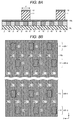
- FIG. 1 is a perspective view of a semiconductor device according to an embodiment.
- FIG. 2 is a cross-sectional view of a memory cell according to an embodiment.
- FIG. 3 is a cross-sectional view depicting a connection example of a bit line in a semiconductor device according to an embodiment.
- FIG. 4 is a plan view showing a connection example of bit lines in a semiconductor device according to an embodiment.
- FIGS. 5A, 5B, and 5C depict aspects of a manufacturing process of a semiconductor device according to an embodiment.
- FIGS. 6A and 6B depict aspects of a manufacturing process of a semiconductor device according to an embodiment
- FIGS. 7A and 7B depict aspects of a manufacturing process of a semiconductor device according to an embodiment.
- FIGS. 8A and 8B depict aspects of a manufacturing process of a semiconductor device according to an embodiment.
- FIGS. 9A and 9B depict aspects of a manufacturing process of a semiconductor device according to an embodiment.
- FIGS. 10A and 10B depict aspects of a manufacturing process of a semiconductor device according to an embodiment.
- FIGS. 11A and 11B depict aspects of a manufacturing process of a semiconductor device according to an embodiment.
- FIGS. 12A and 12B depict aspects of a manufacturing process of a semiconductor device according to an embodiment.
- FIGS. 13A, 13B, and 13C depict aspects of a manufacturing process of a semiconductor device according to an embodiment.
- FIGS. 14A and 14B depict aspects of a manufacturing process of a semiconductor device according to an embodiment.
- FIGS. 15A and 15B depict aspects of a manufacturing process of a semiconductor device according to an embodiment.
- FIGS. 16A and 16B depict aspects of a manufacturing process of a semiconductor device according to an embodiment.
- FIGS. 17A and 17B depict aspects of a manufacturing process of a semiconductor device according to an embodiment.
- a semiconductor device comprises a first periodic pattern comprising first line portions that extend in a first direction and are spaced from each other in a second direction intersecting the first direction at a first interval and a second periodic pattern comprising second line portions that extend in the first direction and are spaced from each other in the second direction at the first interval, the second line portions being between the first line portions in the second direction at one-half the first interval.
- a third pattern is above the first and the second periodic patterns in a third direction intersecting the first and second directions. In a first area, the third pattern includes third line portions spaced from each other in the second direction at the first interval, the third line portions being directly above the second line portions in the third direction within the first area.
- the third pattern In a second area, spaced from the first area in the first direction, the third pattern includes fourth line portions spaced from each other in the second direction at the first interval.
- the fourth line portions are directly above the first line portions in the third direction within the second area.
- a first contact is between the third line portions in the first area and is connected to a first line portion of the first pattern.
- a second contact is between the fourth line portions in the second area and connected to a second line portion of the second pattern.
- a semiconductor device in which a contact can be directly connected to fine wiring at a narrow pitch will be described by taking a cross-point type memory that uses a variable resistance element or the like in a memory cell as one possible, non-limiting particular example.
- the semiconductor device may be devices other than cross-point type memory.
- FIG. 1 is a perspective view showing an overall configuration example of a semiconductor device 1 according to an embodiment.
- the semiconductor device 1 has a structure in which a plurality of memory cells are sandwiched between a plurality of bit lines and a plurality of word lines. These memory cells, bit lines, and word lines are stacked in multiple layers.
- the semiconductor device 1 is configured as a cross-point type memory that uses variable resistance elements in the memory cells. Memory cells stacked in four layers are shown in FIG. 1 ; however, the memory cells may be stacked in any number of layers.
- a plurality of bit lines BLa at a lowermost layer extend in a Y direction and are arranged at a predetermined pitch in an X direction intersecting with the Y direction.
- a plurality of word lines WLc extend in the X direction and are arranged at a predetermined pitch in the Y direction.
- a plurality of word lines WLe extend in the Y direction and are arranged at the predetermined pitch in the X direction.
- a plurality of word lines WLg extend in the X direction and are arranged at the predetermined pitch in the Y direction.
- a plurality of bit lines BLi extend in the Y direction and are arranged at the predetermined pitch in the X direction.
- bit lines and the word lines extend in directions that intersect with each other.
- the pitch of the bit lines and the pitch of the word lines are, for example, equal.
- the bit lines and the word lines are formed of, for example, tungsten (W).
- a plurality of memory cells MCb between the plurality of bit lines BLa and the plurality of word lines WLc. Each memory cell MCb is connected to a bit line BLa and a word line WLc. A plurality of memory cells MCd are between the plurality of word lines WLc and the plurality of bit lines BLe. Each memory cell MCd is connected to a word line WLc and a bit line BLe. A plurality of memory cells MCf are between the plurality of bit lines BLe and the plurality of word lines WLg. Each memory cell MCf is connected to a bit line BLe and a word line WLg. A plurality of memory cells MCh are between the plurality of word lines WLg and the plurality of bit lines BLi. Each memory cell MCh is connected to a word line WLg and a bit line BLi.
- a contact CTa is connected to each bit line BLa. Though not specifically depicted, each contact CTa is connected to an electrode pad, an upper layer wiring, or the like.
- a contact CTc is connected to each word line WLc. Though not specifically depicted, each contact CTc is connected to an electrode pad, an upper layer wiring, or the like.
- a contact CTe is connected to each bit line BLe. Though not specifically depicted, each contact CTe is connected to an electrode pad, an upper layer wiring, or the like.
- a contact CTg is connected to each word line WLg. Though not specifically depicted, each contact CTq is connected to an electrode pad, an upper layer wiring, or the like.
- a contact CTi is connected to each bit line BLi.
- each contact CTi is connected to an electrode pad, an upper layer wiring, or the like.
- the contacts CTa, CTc, CTe, CTg, CTi are formed of, for example, tungsten (W).
- W tungsten
- FIG. 2 shows a cross-sectional view showing a configuration example of memory cells according to an embodiment.
- FIG. 2 shows a cross-sectional view parallel to the Y direction in FIG. 1 .
- the memory cell MCb has a structure in which a non-ohmic element NO, a variable resistance element VR and an electrode EL are stacked in an order from a bit line BLa side toward a word line WLc side.
- the non-ohmic element NO is connected to the bit line BLa
- the electrode EL is connected to the word line WLc.
- the memory cell MCd has a structure in which the electrode EL, the variable resistance element VR and the non-ohmic element NO are stacked in an order from the word line WLc side toward a bit line BLe side.
- the electrode EL is connected to the word line WLc
- the non-ohmic element NO is connected to the bit line BLe.
- the non-ohmic element NO has a Schottky structure, a PN structure, a P + Poly-Silicon-Intrinsic-N + Poly-Silicon (PIN) structure, a Metal-Insulator-Metal (MIM) structure, or a Poly-Si-Insulator-Poly-Si (SIS) structure.
- variable resistance element VR is an element capable of storing data in a nonvolatile manner by changing a resistance value via a current, heat, or chemical energy switching or the otherwise upon application of a voltage.
- a composite compound containing a cation of a transition element, for example, may be used in the variable resistance element VR.
- the composite compound examples include materials having a crystal structure such as a spinel structure (AM 2 O 4 ), an ilmenite structure (AMO 3 ), a delafossite structure (AMO 2 ), a LiMoN 2 structure (AMN 2 ), a wolframite structure (AMO 4 ), an olivine structure (A 2 MO 4 ), a hollandite structure (A x MO 2 ), a ramsdellite structure (A x MO 2 ) and a perovskite structure (AMO 3 ).
- the variable resistance element VR is configured as a Resistive Random Access Memory (ReRAM) or the like whose resistance value is changed by movement of cations.
- ReRAM Resistive Random Access Memory
- FIG. 3 is a cross-sectional view of the semiconductor device 1 .
- FIG. 3 is a cross-sectional view parallel to the X direction in FIG. 1 .
- bit lines BLa, BLe and BLi have the same connection structure, and the bit lines BL shown in FIG. 3 may be any of the bit lines BLa, BLe and BLi.
- the contacts CT shown in FIG. 3 are any one of the contacts CTa, CTe and CTi connected to any of the bit lines BLa, BLe and BLi.
- a lower structure of the bit line BL is depicted in a simplified manner as an under layer UL.
- a connection example of the semiconductor device 1 will be described by taking a bit line BL as an example.
- the word lines WLc and WLg also have a connection structure similar to that of the bit lines BL.
- the bit lines BL are arranged at a predetermined pitch P on the under layer UL.
- the bit line BL has a line-and-space structure in which width of the bit line BL in the X direction and an interval between adjacent bit lines BL are equal.
- the bit line BL has a fine width and the pitch P, which are equal to or less than an exposure limit of an immersion exposure lithography machine that uses, for example, an ArF excimer laser as a light source.
- An interlayer insulation layer IL is disposed between the bit lines BL.
- a stopper layer 20 is disposed on the bit line BL, for example, every other bit line BL so as to cover a bit line BL. That is, stopper layers 20 are disposed in the X direction at a pitch (2P) that is twice the pitch (P) of the bit lines BL.
- the stopper layer 20 is formed of, for example, silicon nitride (SiN).
- the contact CT is connected, for example, to every fifth bit line BL (or at bit lines at a 4 P pitch).
- An upper end of the contact CT has a diameter of 2 P, that is, twice the pitch of the bit lines BL.
- the contact CT is disposed between the stopper layers 20 , and portions of a lower end of the contact CT are on shoulder portions of the stopper layers 20 . Therefore, the lower end of the contact CT is not in contact with the bit lines BL that are on each side of the bit line BL to which the contact CT is connected.
- An electrode pad PD is connected to the upper end of the contact CT.
- Upper layer wiring (not separately depicted) is connected to the electrode pad PD, and the bit line BL is connected to the upper layer wiring via the contact CT and the electrode pad PD.
- the upper layer wiring may be directly connected to the upper end of the contact CT without a distinct electrode pad disposed therebetween.
- a guide layer 10 is disposed on the bit lines BL that are between positions of adjacent stopper layers 20 and to which a contact CT is not connected.
- the guide layer 10 is formed of, for example, silicon oxide (SiO 2 ).
- An interlayer insulation layer 13 is disposed between stopper layers 20 so as to cover the guide layer 10 and portions of the stopper layers 20 .
- the interlayer insulation layer 13 is formed of, for example, SiO 2 .
- the bit lines BL are grouped in groups of four, so that all the bit lines BL can be connected to a contact CT. This is shown in FIG. 4 by the repeating groups of contacts CT- 1 , CT- 2 , CT- 3 , and CT- 4 .
- FIG. 4 In the plan view of FIG. 4 , a range wider than that of the cross-sectional view of FIG. 3 is shown.
- the guide layers 10 , the interlayer insulation layers 13 , the contacts CT, and the electrode pads PD are omitted.
- positions of the contacts CT are indicated by circles.
- the contacts CT are arranged groups of four at both end portions of sets of four adjacent bit lines BL.
- contacts CT- 1 are on a first row and contacts CT- 2 are on a second row.
- the contacts CT- 1 and contacts CT- 2 are in an area AR- 1 and are connected to the bit lines BL- 1 .
- the rows of contacts CT- 1 and contacts CT- 2 are partially offset from one another in the Y-direction.
- Contacts CT- 3 are on a third row and contacts CT- 4 are on a fourth row
- the contacts CT- 3 and contacts CT- 4 are in an area AR- 2 and are connected to bit lines BL- 2 .
- the rows of contacts CT- 3 and contacts CT- 4 are partially offset from one another in the Y-direction.
- the contacts CT- 1 and the contacts CT- 2 alternate with each other along the X direction such that adjacent bit lines BL- 1 are connected to a different one of a contact CT- 1 or a contact CT- 2 .
- the bit lines BL- 2 are between the bit lines BL- 1 , and the bit lines BL- 2 are connected to the contacts CT- 3 and the contacts CT- 4 in alternation such that adjacent bit lines BL- 2 are connected to a different one of a contact CT- 3 or a contact CT- 4 .
- the stopper layers 20 as third patterns are arranged on the bit lines BL in parallel in the Y direction along the bit lines BL in at least the area AR- 1 or area AR- 2 . However, outside the areas AR- 1 , AR- 2 , the stopper layers 20 partially or entirely deviate from the bit lines BL, and have an irregular arrangement like ridge lines of the fingerprint. However, the pitch of the stopper layers 20 is substantially constant inside and outside the areas AR- 1 , AR- 2 .
- the pitch of the stopper layers 20 may be a pitch which is twice the pitch (P) of the bit lines BL, that is, a pitch equal to pitch 2 P.
- stopper layers 20 are disposed on the bit lines BL- 2 and are spaced from each other at the pitch 2 P in the X direction. Accordingly, the bit lines BL- 1 are electrically connected to the contacts CT- 1 , CT- 2 , while the bit lines BL- 2 are not in contact with the contacts CT- 1 , CT- 2 .
- stopper layers 20 are disposed on the bit lines BL- 1 and are spaced from each other at a pitch 2 P in the X direction. Accordingly, the bit lines BL- 2 are electrically connected to the contacts CT- 3 , CT- 4 , while the bit lines BL- 1 are not in contact with the contacts CT- 3 , CT- 4 .
- the guide layer 10 (see FIG. 3 ) is disposed on the bit lines BL and the interlayer insulation layers IL in areas other than where the stopper layers 20 are disposed.
- bit lines BL having the predetermined pitch P are formed on the under layer UL.
- the pitch P of the bit lines BL is equal to or less than the exposure limit of the immersion exposure machine (e.g., stepper) that uses, for example, an ArF excimer laser as a light source.
- Bit lines BL having a pitch P equal to or less than the exposure limit may be formed by using a sidewall process such as a Self-Aligned Quadruple Patterning (SAQP) or Directed Self-Assembly (DSA) lithography or the like.
- bit lines BL may be formed by using a nanoimprint technique, an Extreme Ultra-Violet (EUV) lithography technique, or the like.
- SAQP Self-Aligned Quadruple Patterning
- DSA Directed Self-Assembly
- bit lines BL may be formed by using a nanoimprint technique, an Extreme Ultra-Violet (EUV) lithography technique, or the like
- An insulation layer is formed so as to cover the formed bit lines BL.
- the insulation layer is planarized by using, for example, Chemical Mechanical Polishing (CMP) to form the interlayer insulation layer IL that is embedded between the bit lines BL.
- CMP Chemical Mechanical Polishing
- an insulation layer 10 b is formed by, for example, Chemical Vapor Deposition (CVD).
- the insulation layer 10 b is, for example, a SiO 2 layer.
- a Spin on Carbon (SOC) layer 11 b is formed on the insulation layer 10 b by, for example, spin coating.
- a Spin on Glass (SOG) layer 12 b is formed on the SOC layer 11 b by, for example, spin coating.
- resist patterns 31 are formed by, for example, immersion exposure in which an ArF excimer laser is used as a light source.
- the resist pattern 31 forms a pattern covering a portion of the bit lines BL extending in the Y direction arranged at a pitch 4 P in the X direction.
- the resist pattern 31 is preferably arranged such that one bit line BL is at a center position in the width direction (X direction) of the resist pattern 31 .
- a deviation in the X direction of up to about 1 ⁇ 4 of the pitch P (P/4) could occur.
- FIG. 6B shows a top view taken at this time.
- a range wider than that of the cross-sectional view of FIG. 6A is shown.
- the bit lines BL are indicated by dotted lines.
- the resist patterns 31 are formed in island shapes in two rows at both end of the bit lines BL. At this time, the resist patterns 31 are arranged such that the arrangement of both rows deviates by a distance equal to pitch P.
- the resist patterns 31 are slimmed (trimmed) by, for example, O 2 plasma, and resist patterns 31 s having a width in the X direction equal to the pitch P of the bit lines BL are formed.
- the resist patterns 31 s are used as masks, and the SOG layer 12 b is processed using, for example, Reactive Ion Etching (RIE) to form SOG patterns 12 .
- RIE Reactive Ion Etching
- the SOC patterns 12 are used as masks, and SOC patterns 11 , whose width in the X direction is the same as the pitch P, are formed by using RIE or the like.
- the width of the SOC patterns 11 in the X direction may be adjusted to be equal to the pitch P of the bit lines BL through slimming of the resist patterns 31 , formation of the SOG patterns 12 , and formation of the SOC patterns 11 .
- FIG. 8B shows a top view taken at this time.
- a range wider than that of the cross-sectional view of FIG. 8A is shown.
- the bit lines BL are indicated by dotted lines.
- the SOG patterns 12 and the SOC patterns 11 are formed in island shapes in two rows at both ends of the bit lines BL, The island shapes in the different rows are offset from each other in the X-direction by a distance equal to pitch P.
- the insulation layer 10 b is processed by, for example, a sidewall process.
- the sidewall process is a technique for obtaining a pattern finer than the initial SOC pattern 11 by using the SOC pattern 11 as a core material.
- an insulation layer 21 b that covers the SOG patterns 12 and the SOC patterns 11 is formed on the insulation layer 10 b by, for example, CVD.
- the insulation layer 21 b is, for example, a SiN layer.
- the insulation layer 21 b for example, has a layer thickness equal to the width of the SOC pattern 11 in the X direction.
- the insulation layer 21 b is thinned by etch back using, for example, RIE, to form an insulation layer pattern 21 , with the SOC patterns 11 as a core material now exposed.
- the exposed SOC patterns 11 are removed. Accordingly, the insulation layer pattern 21 that has a line width in the X direction twice that of the bit line BL and has a pitch 2 P in the X direction twice that of the bit lines BL is formed.
- FIG. 10B shows a top view taken at this time.
- top view of FIG. 10B a range wider than that of the cross-sectional view of FIG. 10A is shown.
- the bit lines are indicated by dotted lines.
- the insulation layer pattern 21 is in a ring shape when viewed from above, with the SOC pattern 11 removed to leave a hole therein.
- the insulation layer pattern 21 is used as a mask, the insulation layer 10 b is processed by using, for example, RIE, and then the insulation layer pattern 21 is removed by, for example, wet processing. Accordingly, the guide layer 10 that has a line width in the X direction twice that of the bit line BL and has a pitch 2 P in the X direction twice that of the bit line BL is formed.
- FIG. 11B shows a top view taken at this time.
- the guide layer 10 is in a ring shape like the insulation layer pattern 21 when viewed from above.
- the bit line BL- 2 is exposed in an area corresponding to the area AR- 1
- the bit line BL- 1 is exposed in an area corresponding to the area AR- 2 .
- the guide layer 10 which has a line width in the X direction equal to that of the SOC pattern 11 and a pitch 2 P (1 ⁇ 2 of the pitch 4 P) in the X direction, can be obtained by the sidewall process shown in FIGS. 9A and 9B , FIGS. 10A and 10B , and FIGS. 11A and 11B from the SOC pattern 11 with a line width in the X direction equal to the pitch P and a pitch 4 P equal to that of the original resist pattern 31 .
- a pattern is formed by using directed self-assembly lithography.
- Directed self-assembly lithography is a technique for obtaining a fine pattern by using a self-segregating Block Co-Polymer (BCP).
- BCP Block Co-Polymer
- the PS-b-PMMA is coated over the bit line BL, the interlayer insulation layer IL, and the guide layer 10 .
- the coating thickness of the PS-b-PMMA may be, for example, 30 nm to 90 nm. Then, the PS-b-PMMA is heated at a predetermined temperature for a predetermined time in a nitrogen atmosphere and phase-separates.
- the bit line BL formed of a metal such as W
- the guide layer 10 formed of an insulation material such as SiO 2
- the guide layer 10 functions as a chemical guide pattern in the directed self-assembly of the PS-b-PMMA. More specifically, PS in the PS-b-PMMA preferentially aligns onto the guide layer 10 due the guide layer 10 being a hydrophobic guide pattern.
- PMMA has a high affinity with the more hydrophilic bit line BL, and thus preferentially aligns on the bit lines BL.
- FIG. 12A shows blocks 32 a of PS and blocks 32 b of PMMA which are formed in a self-aligning manner as described above.
- the blocks 32 a , 32 b arrange in a self-aligning manner to already formed materials below. Therefore, as shown in FIG. 12A , the blocks 32 a , 32 b alternately arrange on the adjacent bit lines BL even when a positional deviation (e.g., about P/4) occurs during the forming the resist pattern 31 (shown in FIGS. 6A and 6B ).
- a positional deviation e.g., about P/4
- FIG. 12B shows a top view.
- a range wider than that of the cross-sectional view of FIG. 12A is shown.
- the blocks 32 a , 32 b are also periodically arranged at pitches 2 P.
- the guide layer 10 deviates from the pitch 2 P or the guide layer 10 does not exist.
- the PS-b-PMMA does not self-assembly to match the target pitch 2P, and the blocks 32 a , 32 b generally do not have a periodic arrangement outside the areas AR- 1 and AR- 2 . That is, the blocks 32 a , 32 b are randomly disposed while still maintaining the pitch 2 P due to the selected parameters of the block copolymer.
- a pattern is obtained in which the blocks 32 a , 32 b are periodically arranged at the pitch 2 P in the areas AR- 1 , AR- 2 and outside the areas AR- 1 , AR- 2 , the blocks 32 a , 32 b are randomly arranged while generally maintaining pattern dimensions corresponding to the pitch 2 P.
- the blocks 32 b are selectively removed by using, for example, RIE.
- an insulation layer 20 b covering the blocks 32 a is formed on the bit lines BL and the interlayer insulation layers IL by, for example, CVD.
- the insulation layer 20 b has a layer thickness sufficient to fill the space between the blocks 32 a , for example, half of the pitch of the blocks 32 a (so a layer thickness equal to pitch P).
- the insulation layer 20 b is, for example, a SiN layer.
- the insulation layer 20 b is planarized by, for example, CMP to expose an upper surface of the blocks 32 a . After this planarization, the insulation layer 20 b is divided by the blocks 32 a and thus forms the stopper layers 20 .
- the now exposed blocks 32 a are removed by, for example, O 2 ashing. Accordingly, the stopper layer 20 having a pitch 2 P in the X direction is obtained.
- FIG. 14B shows a top view.
- the stopper layers 20 are formed at positions coinciding with the previously removed blocks 32 b , and have a pattern matching that of the blocks 32 b . That is, a pattern is obtained in which, in the areas AR- 1 , AR- 2 , the stopper layers 20 are periodically arranged at the pitch 2 P, and outside the areas AR- 1 , AR- 2 , the stopper layers 20 are randomly disposed while maintaining the pitch 2 P.
- stopper layers 20 in the area AR- 1 cover the bit lines BL- 2
- stopper layers 20 in the area AR- 2 cover the bit lines BL- 1 .
- an insulation layer 13 b that covers the guide layers 10 and the stopper layers 20 is formed with a desired layer thickness by, for example, CVD.
- an SOC layer 14 b is formed by, for example, spin coating.
- an SOG layer 15 b is formed by, for example, spin coating.
- a resist is coated over the SOG layer 15 b , and a resist pattern 33 is formed by, for example, immersion exposure in which an ArF excimer laser is used as a light source.
- the resist pattern 33 has a hole pattern.
- the holes in the resist pattern 33 having a diameter twice the pitch P of the bit lines BL at positions corresponding to the contacts CT- 1 , CT- 2 , CT- 3 , CT- 4 shown in FIG. 4 .
- the resist pattern 33 is preferably arranged such that a bit line BL is at a center of each hole (opening) of the resist pattern 33 .
- a shift in the X direction of about P/2 is acceptable.
- the resist patterns 33 are used as masks, and the SOG layer 15 b and the SOC layer 14 b are processed using RIE or the like to form SOG pattern 15 and SOC pattern 14 corresponding to hole pattern of the resist patterns 33 .
- the SOC pattern 14 is used as a mask, and the insulation layer 13 b is processed using, for example, RIE to form the interlayer insulation layer 13 .
- insulation layer 13 b is selectively removed while the stopper layer 20 is not.
- a mixed gas of C 4 F 8 , O 2 and Ar, a mixed gas of C 4 F 6, O 2 and Ar, or a mixed gas of C 4 F 8, C 4 F 6 , O 2 and Ar may be used when the stopper layer 20 is silicon nitride or the like and the insulation layer 13 b is silicon oxide or the like.
- the stopper layer 20 is not completely removed, while the insulation layer 13 b and the guide layer 10 , which is made of a same material as that of the insulation layer 13 b , are both removed.
- a hole HL is formed between the stopper layers 20 .
- FIG. 17B shows a top view taken.
- the SOC pattern 14 and the underlying interlayer insulation layer 13 have the holes HL in the positions of the contacts CT- 1 , CT- 2 , CT- 3 , CT- 4 shown in FIG. 4 .
- the area AR- 1 only one of the plurality of bit lines BL- 1 is exposed in each hole HL.
- the area AR- 2 only one of the plurality of bit lines BL- 2 is exposed in each hole HL.
- the SOC pattern 14 is removed, and a conductive material, such as tungsten (W), is embedded in the holes HL to form the contacts CT- 1 , CT- 2 , CT- 3 , CT- 4 .
- a conductive material such as tungsten (W)
- wiring connected to these elements may take on a fine, narrow-pitched and periodic arrangement such as a line-and-space structure.
- an electrode pad or the like having a size larger than that of the wiring is led out from the wiring, and the electrode pad and the contact are connected to each other, thereby obtaining an indirect electrical connection between the wiring and the contact.
- a memory cell and wiring connected to the memory cell are stacked in a multilayer manner, such as the cross-point type memory, such an adverse effect appears even more significantly.
- the contacts are directly connected to a bit line BL while unintended contact between the contact with the adjacent bit lines BL is avoided by the presence of the stopper layer(s) 20 . Accordingly, it is not required to lead out to an electrode pad having a larger size than the bit line BL, and thus the area of the cell array can be increased, and the size of the semiconductor device 1 can be reduced.
- a contact having a diameter larger than the pitch P of the bit line BL can be directly connected to the bit line BL.
- contact with other bit lines BL is prevented by the stopper layer 20 , so problems associated with positional shift can be reduced.
- the stopper layer 20 is formed by using directed self-assembly lithography. Accordingly, the stopper layer 20 can be reliably disposed on desired bit lines BL, and a short circuit between the contact and the bit lines BL adjacent to the bit line BL connected to the contact can be prevented.
- the guide layer 10 which is a guide pattern used in the directed self-assembly lithography, is formed by, for example, a sidewall process. Accordingly, the fine and narrow-pitched guide layer 10 can be obtained more easily. Even when a slight positional shift occurs in the resist pattern 31 used for forming the guide layer 10 , the influence of the positional shift can be reduced by using the directed self-assembly lithography thereafter.
- the memory cell has a structure in which the non-ohmic element NO, the variable resistance element VR, and the electrode EL are stacked in this order from the bit line side toward the word line side, but the present disclosure is not limited thereto.
- the memory cell may have a structure in which the electrode, the variable resistance element, and the non-ohmic element are stacked in this order from the bit line side toward the word line side.
- the current density in the variable resistance element may be increased by progressively reducing cross-sectional areas of the non-ohmic element, the variable resistance element and the electrode.
- the guide layer 10 is formed by using a sidewall process, but the present disclosure is not limited thereto.
- the guide layer may be formed by using directed self-assembly lithography, nanoimprint techniques, an EUV exposure technique, or other available patterning techniques.
- the semiconductor device 1 is a cross-point type memory, but the present disclosure is not limited thereto.
- the concepts of the example embodiment may be applied to fine and narrow-pitched wiring having a periodic arrangement in a memory device, a logic device having transistors, or any microelectronic devices.
Landscapes
- Engineering & Computer Science (AREA)
- Chemical & Material Sciences (AREA)
- Materials Engineering (AREA)
- Manufacturing & Machinery (AREA)
- Internal Circuitry In Semiconductor Integrated Circuit Devices (AREA)
- Semiconductor Memories (AREA)
- Exposure And Positioning Against Photoresist Photosensitive Materials (AREA)
- Exposure Of Semiconductors, Excluding Electron Or Ion Beam Exposure (AREA)
- Physics & Mathematics (AREA)
- Geometry (AREA)
Abstract
Description
Claims (20)
Applications Claiming Priority (2)
| Application Number | Priority Date | Filing Date | Title |
|---|---|---|---|
| JP2019007517A JP2020119929A (en) | 2019-01-21 | 2019-01-21 | Semiconductor device |
| JP2019-007517 | 2019-01-21 |
Publications (2)
| Publication Number | Publication Date |
|---|---|
| US20200234735A1 US20200234735A1 (en) | 2020-07-23 |
| US10847191B2 true US10847191B2 (en) | 2020-11-24 |
Family
ID=71609055
Family Applications (1)
| Application Number | Title | Priority Date | Filing Date |
|---|---|---|---|
| US16/553,505 Active US10847191B2 (en) | 2019-01-21 | 2019-08-28 | Semiconductor device |
Country Status (4)
| Country | Link |
|---|---|
| US (1) | US10847191B2 (en) |
| JP (1) | JP2020119929A (en) |
| CN (1) | CN111463216B (en) |
| TW (1) | TWI725453B (en) |
Families Citing this family (1)
| Publication number | Priority date | Publication date | Assignee | Title |
|---|---|---|---|---|
| CN113517291B (en) * | 2021-04-19 | 2023-08-29 | 长鑫存储技术有限公司 | Semiconductor structure and forming method thereof |
Citations (11)
| Publication number | Priority date | Publication date | Assignee | Title |
|---|---|---|---|---|
| US20080308954A1 (en) * | 2007-06-12 | 2008-12-18 | Seok-Chang Seo | Semiconductor device and method of forming the same |
| US20100038616A1 (en) | 2008-08-13 | 2010-02-18 | Kabushiki Kaisha Toshiba | Nonvolatile semiconductor memory device and producing method thereof |
| JP2011077475A (en) | 2009-10-02 | 2011-04-14 | Toshiba Corp | Contact forming method and method for manufacturing semiconductor device |
| US8391042B2 (en) * | 2009-01-06 | 2013-03-05 | Samsung Electronics Co., Ltd. | Memory device having sub-bit lines and memory system |
| US8644046B2 (en) * | 2009-02-10 | 2014-02-04 | Samsung Electronics Co., Ltd. | Non-volatile memory devices including vertical NAND channels and methods of forming the same |
| US8791448B2 (en) * | 2007-03-27 | 2014-07-29 | Samsung Electronics Co., Ltd. | Semiconductor memory devices having strapping contacts |
| JP2014154829A (en) | 2013-02-13 | 2014-08-25 | Panasonic Corp | Method for forming structure with contact |
| US9535329B2 (en) | 2014-09-16 | 2017-01-03 | Commissariat à l'énergie atomique et aux énergies alternatives | Grapho-epitaxy method for making patterns on the surface of a substrate |
| US20170263551A1 (en) | 2014-12-24 | 2017-09-14 | Intel Corporation | Novel method for creating alternate hardmask cap interconnect structure with increased overlay margin |
| US20170263511A1 (en) | 2016-03-11 | 2017-09-14 | Leonard TEDESCHI | Wafer processing tool having a micro sensor |
| US20190043754A1 (en) | 2015-06-12 | 2019-02-07 | International Business Machines Corporation | Chemoepitaxy etch trim using a self aligned hard mask for metal line to via |
Family Cites Families (8)
| Publication number | Priority date | Publication date | Assignee | Title |
|---|---|---|---|---|
| JP3634735B2 (en) * | 2000-10-05 | 2005-03-30 | 三洋電機株式会社 | Semiconductor device and semiconductor module |
| JP2003158205A (en) * | 2001-11-26 | 2003-05-30 | Hitachi Ltd | Semiconductor device and manufacturing method |
| DE10240436C1 (en) * | 2002-09-02 | 2003-12-18 | Infineon Technologies Ag | Bit line structure comprises a surface bit line, a trenched bit line, a trench isolation layer, a covering isolation layer, covering connecting layers, and self-adjusting connecting layers |
| TWI489519B (en) * | 2004-04-28 | 2015-06-21 | 半導體能源研究所股份有限公司 | Wiring on substrate, semiconductor device and method of manufacturing same |
| JP2011243790A (en) * | 2010-05-19 | 2011-12-01 | Panasonic Electric Works Co Ltd | Wiring method, structure provided wiring on surface, semiconductor device, wiring board, memory card, electric device, module, and multilayer circuit board |
| KR102395192B1 (en) * | 2015-11-27 | 2022-05-06 | 삼성전자주식회사 | Semiconductor device having air spacers and method for manufacturing the same |
| WO2018047861A1 (en) * | 2016-09-08 | 2018-03-15 | 凸版印刷株式会社 | Wiring board and method for manufacturing wiring board |
| CN108520876B (en) * | 2018-06-26 | 2023-07-11 | 长鑫存储技术有限公司 | Integrated circuit memory and its manufacturing method, semiconductor device |
-
2019
- 2019-01-21 JP JP2019007517A patent/JP2020119929A/en active Pending
- 2019-06-21 TW TW108121671A patent/TWI725453B/en active
- 2019-07-18 CN CN201910649316.6A patent/CN111463216B/en active Active
- 2019-08-28 US US16/553,505 patent/US10847191B2/en active Active
Patent Citations (12)
| Publication number | Priority date | Publication date | Assignee | Title |
|---|---|---|---|---|
| US8791448B2 (en) * | 2007-03-27 | 2014-07-29 | Samsung Electronics Co., Ltd. | Semiconductor memory devices having strapping contacts |
| US20080308954A1 (en) * | 2007-06-12 | 2008-12-18 | Seok-Chang Seo | Semiconductor device and method of forming the same |
| US20100038616A1 (en) | 2008-08-13 | 2010-02-18 | Kabushiki Kaisha Toshiba | Nonvolatile semiconductor memory device and producing method thereof |
| JP2010045205A (en) | 2008-08-13 | 2010-02-25 | Toshiba Corp | Nonvolatile semiconductor memory device, and method of manufacturing the same |
| US8391042B2 (en) * | 2009-01-06 | 2013-03-05 | Samsung Electronics Co., Ltd. | Memory device having sub-bit lines and memory system |
| US8644046B2 (en) * | 2009-02-10 | 2014-02-04 | Samsung Electronics Co., Ltd. | Non-volatile memory devices including vertical NAND channels and methods of forming the same |
| JP2011077475A (en) | 2009-10-02 | 2011-04-14 | Toshiba Corp | Contact forming method and method for manufacturing semiconductor device |
| JP2014154829A (en) | 2013-02-13 | 2014-08-25 | Panasonic Corp | Method for forming structure with contact |
| US9535329B2 (en) | 2014-09-16 | 2017-01-03 | Commissariat à l'énergie atomique et aux énergies alternatives | Grapho-epitaxy method for making patterns on the surface of a substrate |
| US20170263551A1 (en) | 2014-12-24 | 2017-09-14 | Intel Corporation | Novel method for creating alternate hardmask cap interconnect structure with increased overlay margin |
| US20190043754A1 (en) | 2015-06-12 | 2019-02-07 | International Business Machines Corporation | Chemoepitaxy etch trim using a self aligned hard mask for metal line to via |
| US20170263511A1 (en) | 2016-03-11 | 2017-09-14 | Leonard TEDESCHI | Wafer processing tool having a micro sensor |
Also Published As
| Publication number | Publication date |
|---|---|
| TWI725453B (en) | 2021-04-21 |
| CN111463216B (en) | 2023-06-02 |
| JP2020119929A (en) | 2020-08-06 |
| TW202029856A (en) | 2020-08-01 |
| US20200234735A1 (en) | 2020-07-23 |
| CN111463216A (en) | 2020-07-28 |
Similar Documents
| Publication | Publication Date | Title |
|---|---|---|
| CN107887393B (en) | Memory device with single bottom electrode layer | |
| CN109786549B (en) | Resistive random access memory device | |
| US9466794B2 (en) | Low form voltage resistive random access memory (RRAM) | |
| US8987909B2 (en) | Method of manufacturing electronic component | |
| KR102255723B1 (en) | Rram with a barrier layer | |
| JP2017195360A (en) | Resistance change type memory device having height increased data storage layer | |
| JP2006511965A (en) | Improved method for fabricating high density non-volatile memory | |
| KR20110117069A (en) | Resistive features and removable spacer pitch doubling patterning method for columnar structures | |
| US8835897B2 (en) | Nonvolatile memory device having variable resistance memory cells | |
| US8729667B2 (en) | Non-volatile memory device and method of manufacturing the same | |
| US20210013408A1 (en) | Resistive random access memories and method for fabricating the same | |
| US20100248422A1 (en) | Method of manufacturing nonvolatile memory device | |
| US20110233502A1 (en) | Nonvolatile memory device | |
| KR20220000374A (en) | Memory device and method for fabricating the same | |
| US9252192B2 (en) | Methods of manufacturing semiconductor devices including a cross point cell array | |
| WO2024027623A1 (en) | Three dimensional cross-point non-volatile memory | |
| US9257486B2 (en) | RRAM array having lateral RRAM cells and vertical conducting structures | |
| US10847191B2 (en) | Semiconductor device | |
| US11114614B2 (en) | Process for fabricating resistive memory cells | |
| KR20250176580A (en) | New process technology for embedded memory | |
| US10164183B2 (en) | Semiconductor device and manufacturing method thereof | |
| US20140021432A1 (en) | Variable resistance memory device and method for fabricating the same | |
| US20250241213A1 (en) | Semiconductor device including plug electrode with nanorods and method of manufacturing the same | |
| CN117015236A (en) | semiconductor memory device |
Legal Events
| Date | Code | Title | Description |
|---|---|---|---|
| FEPP | Fee payment procedure |
Free format text: ENTITY STATUS SET TO UNDISCOUNTED (ORIGINAL EVENT CODE: BIG.); ENTITY STATUS OF PATENT OWNER: LARGE ENTITY |
|
| AS | Assignment |
Owner name: TOSHIBA MEMORY CORPORATION, JAPAN Free format text: ASSIGNMENT OF ASSIGNORS INTEREST;ASSIGNOR:KASAHARA, YUSUKE;REEL/FRAME:051251/0485 Effective date: 20191126 |
|
| STPP | Information on status: patent application and granting procedure in general |
Free format text: NOTICE OF ALLOWANCE MAILED -- APPLICATION RECEIVED IN OFFICE OF PUBLICATIONS |
|
| STPP | Information on status: patent application and granting procedure in general |
Free format text: PUBLICATIONS -- ISSUE FEE PAYMENT VERIFIED |
|
| STCF | Information on status: patent grant |
Free format text: PATENTED CASE |
|
| AS | Assignment |
Owner name: KIOXIA CORPORATION, JAPAN Free format text: CHANGE OF NAME AND ADDRESS;ASSIGNOR:TOSHIBA MEMORY CORPORATION;REEL/FRAME:058905/0582 Effective date: 20191001 |
|
| MAFP | Maintenance fee payment |
Free format text: PAYMENT OF MAINTENANCE FEE, 4TH YEAR, LARGE ENTITY (ORIGINAL EVENT CODE: M1551); ENTITY STATUS OF PATENT OWNER: LARGE ENTITY Year of fee payment: 4 |