US10844065B2 - Heterocyclic compound, and organic electroluminescence device and organic electroluminescence display device including the same - Google Patents
Heterocyclic compound, and organic electroluminescence device and organic electroluminescence display device including the same Download PDFInfo
- Publication number
- US10844065B2 US10844065B2 US15/963,036 US201815963036A US10844065B2 US 10844065 B2 US10844065 B2 US 10844065B2 US 201815963036 A US201815963036 A US 201815963036A US 10844065 B2 US10844065 B2 US 10844065B2
- Authority
- US
- United States
- Prior art keywords
- substituted
- carbon atoms
- group
- ring
- unsubstituted
- Prior art date
- Legal status (The legal status is an assumption and is not a legal conclusion. Google has not performed a legal analysis and makes no representation as to the accuracy of the status listed.)
- Active, expires
Links
- 238000005401 electroluminescence Methods 0.000 title claims abstract description 86
- 150000002391 heterocyclic compounds Chemical class 0.000 title claims abstract description 59
- 125000004432 carbon atom Chemical group C* 0.000 claims description 80
- 150000001875 compounds Chemical class 0.000 claims description 57
- 125000003118 aryl group Chemical group 0.000 claims description 45
- 230000005525 hole transport Effects 0.000 claims description 45
- 125000000217 alkyl group Chemical group 0.000 claims description 27
- 125000001072 heteroaryl group Chemical group 0.000 claims description 25
- 125000004435 hydrogen atom Chemical group [H]* 0.000 claims description 24
- 229910052805 deuterium Inorganic materials 0.000 claims description 20
- 125000004431 deuterium atom Chemical group 0.000 claims description 20
- 239000002019 doping agent Substances 0.000 claims description 12
- 125000001997 phenyl group Chemical group [H]C1=C([H])C([H])=C(*)C([H])=C1[H] 0.000 claims description 12
- 229910052717 sulfur Inorganic materials 0.000 claims description 9
- 125000000732 arylene group Chemical group 0.000 claims description 8
- 125000005549 heteroarylene group Chemical group 0.000 claims description 8
- 125000002496 methyl group Chemical group [H]C([H])([H])* 0.000 claims description 6
- 229910052760 oxygen Inorganic materials 0.000 claims description 5
- 125000005264 aryl amine group Chemical group 0.000 claims description 4
- 239000010410 layer Substances 0.000 description 179
- IWZSHWBGHQBIML-ZGGLMWTQSA-N (3S,8S,10R,13S,14S,17S)-17-isoquinolin-7-yl-N,N,10,13-tetramethyl-2,3,4,7,8,9,11,12,14,15,16,17-dodecahydro-1H-cyclopenta[a]phenanthren-3-amine Chemical compound CN(C)[C@H]1CC[C@]2(C)C3CC[C@@]4(C)[C@@H](CC[C@@H]4c4ccc5ccncc5c4)[C@@H]3CC=C2C1 IWZSHWBGHQBIML-ZGGLMWTQSA-N 0.000 description 110
- YMWUJEATGCHHMB-UHFFFAOYSA-N Dichloromethane Chemical compound ClCCl YMWUJEATGCHHMB-UHFFFAOYSA-N 0.000 description 102
- -1 3,3-dimethylbutyl Chemical group 0.000 description 77
- 239000012044 organic layer Substances 0.000 description 51
- 239000000463 material Substances 0.000 description 46
- XLYOFNOQVPJJNP-UHFFFAOYSA-N water Substances O XLYOFNOQVPJJNP-UHFFFAOYSA-N 0.000 description 35
- RTZKZFJDLAIYFH-UHFFFAOYSA-N Diethyl ether Chemical compound CCOCC RTZKZFJDLAIYFH-UHFFFAOYSA-N 0.000 description 34
- CSNNHWWHGAXBCP-UHFFFAOYSA-L Magnesium sulfate Chemical compound [Mg+2].[O-][S+2]([O-])([O-])[O-] CSNNHWWHGAXBCP-UHFFFAOYSA-L 0.000 description 34
- 238000002347 injection Methods 0.000 description 26
- 239000007924 injection Substances 0.000 description 26
- 239000010409 thin film Substances 0.000 description 25
- 230000015572 biosynthetic process Effects 0.000 description 22
- 238000003786 synthesis reaction Methods 0.000 description 22
- YXFVVABEGXRONW-UHFFFAOYSA-N Toluene Chemical compound CC1=CC=CC=C1 YXFVVABEGXRONW-UHFFFAOYSA-N 0.000 description 21
- 238000006243 chemical reaction Methods 0.000 description 21
- 239000004065 semiconductor Substances 0.000 description 21
- 238000000034 method Methods 0.000 description 19
- 101100214488 Solanum lycopersicum TFT2 gene Proteins 0.000 description 17
- 238000004440 column chromatography Methods 0.000 description 17
- 239000012043 crude product Substances 0.000 description 17
- 238000000605 extraction Methods 0.000 description 17
- 229910052943 magnesium sulfate Inorganic materials 0.000 description 17
- 239000003208 petroleum Substances 0.000 description 17
- 239000012299 nitrogen atmosphere Substances 0.000 description 16
- 238000003756 stirring Methods 0.000 description 16
- 0 C.C.C.C.CCC.CC[Y][Y].[1*]C1=C([2*])N=C2C(=N1)C(C)=C1C=C([3*])C([4*])=CC1=C2C.[2H][2H]*C Chemical compound C.C.C.C.CCC.CC[Y][Y].[1*]C1=C([2*])N=C2C(=N1)C(C)=C1C=C([3*])C([4*])=CC1=C2C.[2H][2H]*C 0.000 description 14
- 101100489584 Solanum lycopersicum TFT1 gene Proteins 0.000 description 14
- 239000012153 distilled water Substances 0.000 description 14
- 239000000758 substrate Substances 0.000 description 14
- 239000007795 chemical reaction product Substances 0.000 description 12
- 239000002356 single layer Substances 0.000 description 12
- 239000000872 buffer Substances 0.000 description 10
- 239000011541 reaction mixture Substances 0.000 description 10
- QTBSBXVTEAMEQO-UHFFFAOYSA-N Acetic acid Chemical compound CC(O)=O QTBSBXVTEAMEQO-UHFFFAOYSA-N 0.000 description 9
- 230000002349 favourable effect Effects 0.000 description 9
- 239000011229 interlayer Substances 0.000 description 9
- 229910052751 metal Inorganic materials 0.000 description 9
- 239000002184 metal Substances 0.000 description 9
- MFRIHAYPQRLWNB-UHFFFAOYSA-N sodium tert-butoxide Chemical compound [Na+].CC(C)(C)[O-] MFRIHAYPQRLWNB-UHFFFAOYSA-N 0.000 description 9
- PCLIMKBDDGJMGD-UHFFFAOYSA-N N-bromosuccinimide Chemical compound BrN1C(=O)CCC1=O PCLIMKBDDGJMGD-UHFFFAOYSA-N 0.000 description 8
- 230000000903 blocking effect Effects 0.000 description 8
- XLOMVQKBTHCTTD-UHFFFAOYSA-N Zinc monoxide Chemical compound [Zn]=O XLOMVQKBTHCTTD-UHFFFAOYSA-N 0.000 description 7
- 239000000203 mixture Substances 0.000 description 7
- 229920000767 polyaniline Polymers 0.000 description 6
- BWHMMNNQKKPAPP-UHFFFAOYSA-L potassium carbonate Chemical compound [K+].[K+].[O-]C([O-])=O BWHMMNNQKKPAPP-UHFFFAOYSA-L 0.000 description 6
- 125000001424 substituent group Chemical group 0.000 description 6
- 239000011701 zinc Substances 0.000 description 6
- ZOXJGFHDIHLPTG-UHFFFAOYSA-N Boron Chemical group [B] ZOXJGFHDIHLPTG-UHFFFAOYSA-N 0.000 description 5
- OKTJSMMVPCPJKN-UHFFFAOYSA-N Carbon Chemical compound [C] OKTJSMMVPCPJKN-UHFFFAOYSA-N 0.000 description 5
- 229910052782 aluminium Inorganic materials 0.000 description 5
- 239000003990 capacitor Substances 0.000 description 5
- 229910052799 carbon Inorganic materials 0.000 description 5
- 230000001965 increasing effect Effects 0.000 description 5
- 239000011810 insulating material Substances 0.000 description 5
- 229910052757 nitrogen Inorganic materials 0.000 description 5
- 238000002161 passivation Methods 0.000 description 5
- 238000010992 reflux Methods 0.000 description 5
- VYPSYNLAJGMNEJ-UHFFFAOYSA-N silicon dioxide Inorganic materials O=[Si]=O VYPSYNLAJGMNEJ-UHFFFAOYSA-N 0.000 description 5
- 239000002904 solvent Substances 0.000 description 5
- GHYOCDFICYLMRF-UTIIJYGPSA-N (2S,3R)-N-[(2S)-3-(cyclopenten-1-yl)-1-[(2R)-2-methyloxiran-2-yl]-1-oxopropan-2-yl]-3-hydroxy-3-(4-methoxyphenyl)-2-[[(2S)-2-[(2-morpholin-4-ylacetyl)amino]propanoyl]amino]propanamide Chemical compound C1(=CCCC1)C[C@@H](C(=O)[C@@]1(OC1)C)NC([C@H]([C@@H](C1=CC=C(C=C1)OC)O)NC([C@H](C)NC(CN1CCOCC1)=O)=O)=O GHYOCDFICYLMRF-UTIIJYGPSA-N 0.000 description 4
- WZZBNLYBHUDSHF-DHLKQENFSA-N 1-[(3s,4s)-4-[8-(2-chloro-4-pyrimidin-2-yloxyphenyl)-7-fluoro-2-methylimidazo[4,5-c]quinolin-1-yl]-3-fluoropiperidin-1-yl]-2-hydroxyethanone Chemical compound CC1=NC2=CN=C3C=C(F)C(C=4C(=CC(OC=5N=CC=CN=5)=CC=4)Cl)=CC3=C2N1[C@H]1CCN(C(=O)CO)C[C@@H]1F WZZBNLYBHUDSHF-DHLKQENFSA-N 0.000 description 4
- UJOBWOGCFQCDNV-UHFFFAOYSA-N 9H-carbazole Chemical compound C1=CC=C2C3=CC=CC=C3NC2=C1 UJOBWOGCFQCDNV-UHFFFAOYSA-N 0.000 description 4
- PJNZQBXNNUPREV-UHFFFAOYSA-N C.C.C.C.C1=CC2=C(C=C1)N(C1=C3N=CC=NC3=C(N3C4=C(C=CC=C4)C4=C3C=CC=C4)C3=C1N=CC=N3)C1=C2C=CC=C1.C1=CC2=C(C=C1)N(C1=C3N=CC=NC3=C(N3C4=C(C=CC=C4)OC4=C3C=CC=C4)C3=C1N=CC=N3)C1=C(C=CC=C1)O2.C1=CC2=C(C=C1)N(C1=CC3=C(C=C1)N(C1=C4N=CC=NC4=C(N4C5=C(C=C(N6C7=C(C=CC=C7)C7=C6C=CC=C7)C=C5)C5=C4C=CC(N4C6=C(C=CC=C6)C6=C4C=CC=C6)=C5)C4=C1N=CC=N4)C1=C3C=C(N3C4=C(C=CC=C4)C4=C3C=CC=C4)C=C1)C1=C2C=CC=C1.C1=CC2=C3C(=C1)N=CN(C1=C4C=CC=CC4=C(N4C=N/C5=C/C=C\C6=CC=CC4=C65)C4=C1N=CC=N4)/C3=C/C=C\2.C1=CC2=CC=C(N(C3=CC=C4C=CC=CC4=C3)C3=C4N=CC=NC4=C(N(C4=CC5=C(C=CC=C5)C=C4)C4=CC5=C(C=CC=C5)C=C4)C4=C3N=CC=N4)C=C2C=C1.C1=CC=C(C2=CC=C(N(C3=CC=C(C4=CC=CC=C4)C=C3)C3=C4N=CC=NC4=C(N(C4=CC=C(C5=CC=CC=C5)C=C4)C4=CC=C(C5=CC=CC=C5)C=C4)C4=C3N=CC=N4)C=C2)C=C1.C1=CC=C(N(C2=CC=CC=C2)C2=C3N=CC=NC3=C(N(C3=CC=CC=C3)C3=CC=CC=C3)C3=C2N=CC=N3)C=C1.C1=CC=C(N2C3=C(C=CC=C3)N(C3=C4N=CC=NC4=C(N4C5=C(C=CC=C5)N(C5=CC=CC=C5)C5=C4C=CC=C5)C4=C3N=CC=N4)C3=C2C=CC=C3)C=C1 Chemical compound C.C.C.C.C1=CC2=C(C=C1)N(C1=C3N=CC=NC3=C(N3C4=C(C=CC=C4)C4=C3C=CC=C4)C3=C1N=CC=N3)C1=C2C=CC=C1.C1=CC2=C(C=C1)N(C1=C3N=CC=NC3=C(N3C4=C(C=CC=C4)OC4=C3C=CC=C4)C3=C1N=CC=N3)C1=C(C=CC=C1)O2.C1=CC2=C(C=C1)N(C1=CC3=C(C=C1)N(C1=C4N=CC=NC4=C(N4C5=C(C=C(N6C7=C(C=CC=C7)C7=C6C=CC=C7)C=C5)C5=C4C=CC(N4C6=C(C=CC=C6)C6=C4C=CC=C6)=C5)C4=C1N=CC=N4)C1=C3C=C(N3C4=C(C=CC=C4)C4=C3C=CC=C4)C=C1)C1=C2C=CC=C1.C1=CC2=C3C(=C1)N=CN(C1=C4C=CC=CC4=C(N4C=N/C5=C/C=C\C6=CC=CC4=C65)C4=C1N=CC=N4)/C3=C/C=C\2.C1=CC2=CC=C(N(C3=CC=C4C=CC=CC4=C3)C3=C4N=CC=NC4=C(N(C4=CC5=C(C=CC=C5)C=C4)C4=CC5=C(C=CC=C5)C=C4)C4=C3N=CC=N4)C=C2C=C1.C1=CC=C(C2=CC=C(N(C3=CC=C(C4=CC=CC=C4)C=C3)C3=C4N=CC=NC4=C(N(C4=CC=C(C5=CC=CC=C5)C=C4)C4=CC=C(C5=CC=CC=C5)C=C4)C4=C3N=CC=N4)C=C2)C=C1.C1=CC=C(N(C2=CC=CC=C2)C2=C3N=CC=NC3=C(N(C3=CC=CC=C3)C3=CC=CC=C3)C3=C2N=CC=N3)C=C1.C1=CC=C(N2C3=C(C=CC=C3)N(C3=C4N=CC=NC4=C(N4C5=C(C=CC=C5)N(C5=CC=CC=C5)C5=C4C=CC=C5)C4=C3N=CC=N4)C3=C2C=CC=C3)C=C1 PJNZQBXNNUPREV-UHFFFAOYSA-N 0.000 description 4
- FFQAXHKNHKDWGW-UHFFFAOYSA-N C.C.C1=CC2=C(C3=C4N=CC=NC4=C(C4=C5C=CC=CC5=C(N5C6=C(C=CC=C6)C6=C5C=CC=C6)S4)C4=C3N=CC=N4)SC(N3C4=C(C=CC=C4)C4=C3C=CC=C4)=C2C=C1.C1=CC2=C(C=C1)N(C1=C3N=CC=NC3=C(N3C4=C(C=CC=C4)SC4=C3C=CC=C4)C3=C1N=CC=N3)C1=C(C=CC=C1)S2.C1=CC2=C(C=C1)N(C1=CC=C(C3=C4N=CC=NC4=C(C4=CC=C(N5C6=C(C=CC=C6)C6=C5C=CC=C6)C=C4)C4=C3N=CC=N4)C=C1)C1=C2C=CC=C1.C1=CC2=C(C=C1)N(C1=CC=C(C3=C4N=CC=NC4=C(C4=CC=C(N5C6=C(C=CC=C6)C6=C5C=CC=C6)S4)C4=C3N=CC=N4)S1)C1=C2C=CC=C1.C1=CC2=CC=C(N(C3=CC=C4C=CC=CC4=C3)C3=C4C=CC=CC4=C(C4=C5N=CC=NC5=C(C5=C6C=CC=CC6=C(N(C6=CC7=C(C=CC=C7)C=C6)C6=CC7=C(C=CC=C7)C=C6)S5)C5=C4N=CC=N5)S3)C=C2C=C1.C1=CC2=CC=C(N(C3=CC=C4C=CC=CC4=C3)C3=CC=C(C4=C5N=CC=NC5=C(C5=CC=C(N(C6=CC7=C(C=CC=C7)C=C6)C6=CC7=C(C=CC=C7)C=C6)S5)C5=C4N=CC=N5)S3)C=C2C=C1.C1=CC=C(C2=NC3=C(N=C2C2=CC=CC=C2)C(C2=CC=C(C4=CC=C(N(C5=CC=CC=C5)C5=CC=CC=C5)C=C4)S2)=C2N=C(C4=CC=CC=C4)C(C4=CC=CC=C4)=NC2=C3C2=CC=C(C3=CC=C(N(C4=CC=CC=C4)C4=CC=CC=C4)C=C3)S2)C=C1.C1=CC=C(N(C2=CC=CC=C2)C2=C3C=CC=CC3=C(C3=C4N=CC=NC4=C(C4=C5C=CC=CC5=C(N(C5=CC=CC=C5)C5=CC=CC=C5)S4)C4=C3N=CC=N4)S2)C=C1.C1=CC=C(N(C2=CC=CC=C2)C2=CC=C(C3=C4N=CC=NC4=C(C4=CC=C(N(C5=CC=C6C=CC=CC6=C5)C5=CC=C6C=CC=CC6=C5)C=C4)C4=C3N=CC=N4)C=C2)C=C1.C1=CC=C(N(C2=CC=CC=C2)C2=CC=C(C3=C4N=CC=NC4=C(C4=CC=C(N(C5=CC=CC=C5)C5=CC=CC=C5)C=C4)C4=C3N=CC=N4)C=C2)C=C1.C1=CC=C(N(C2=CC=CC=C2)C2=CC=C(C3=C4N=CC=NC4=C(C4=CC=C(N(C5=CC=CC=C5)C5=CC=CC=C5)S4)C4=C3N=CC=N4)S2)C=C1.C1=CC=C(N(C2=CC=CC=C2)C2=CC=C(C3=CC=C(C4=C5N=CC=NC5=C(C5=CC=C(C6=CC=C(N(C7=CC=CC=C7)C7=CC=CC=C7)C=C6)S5)C5=C4N=CC=N5)S3)C=C2)C=C1 Chemical compound C.C.C1=CC2=C(C3=C4N=CC=NC4=C(C4=C5C=CC=CC5=C(N5C6=C(C=CC=C6)C6=C5C=CC=C6)S4)C4=C3N=CC=N4)SC(N3C4=C(C=CC=C4)C4=C3C=CC=C4)=C2C=C1.C1=CC2=C(C=C1)N(C1=C3N=CC=NC3=C(N3C4=C(C=CC=C4)SC4=C3C=CC=C4)C3=C1N=CC=N3)C1=C(C=CC=C1)S2.C1=CC2=C(C=C1)N(C1=CC=C(C3=C4N=CC=NC4=C(C4=CC=C(N5C6=C(C=CC=C6)C6=C5C=CC=C6)C=C4)C4=C3N=CC=N4)C=C1)C1=C2C=CC=C1.C1=CC2=C(C=C1)N(C1=CC=C(C3=C4N=CC=NC4=C(C4=CC=C(N5C6=C(C=CC=C6)C6=C5C=CC=C6)S4)C4=C3N=CC=N4)S1)C1=C2C=CC=C1.C1=CC2=CC=C(N(C3=CC=C4C=CC=CC4=C3)C3=C4C=CC=CC4=C(C4=C5N=CC=NC5=C(C5=C6C=CC=CC6=C(N(C6=CC7=C(C=CC=C7)C=C6)C6=CC7=C(C=CC=C7)C=C6)S5)C5=C4N=CC=N5)S3)C=C2C=C1.C1=CC2=CC=C(N(C3=CC=C4C=CC=CC4=C3)C3=CC=C(C4=C5N=CC=NC5=C(C5=CC=C(N(C6=CC7=C(C=CC=C7)C=C6)C6=CC7=C(C=CC=C7)C=C6)S5)C5=C4N=CC=N5)S3)C=C2C=C1.C1=CC=C(C2=NC3=C(N=C2C2=CC=CC=C2)C(C2=CC=C(C4=CC=C(N(C5=CC=CC=C5)C5=CC=CC=C5)C=C4)S2)=C2N=C(C4=CC=CC=C4)C(C4=CC=CC=C4)=NC2=C3C2=CC=C(C3=CC=C(N(C4=CC=CC=C4)C4=CC=CC=C4)C=C3)S2)C=C1.C1=CC=C(N(C2=CC=CC=C2)C2=C3C=CC=CC3=C(C3=C4N=CC=NC4=C(C4=C5C=CC=CC5=C(N(C5=CC=CC=C5)C5=CC=CC=C5)S4)C4=C3N=CC=N4)S2)C=C1.C1=CC=C(N(C2=CC=CC=C2)C2=CC=C(C3=C4N=CC=NC4=C(C4=CC=C(N(C5=CC=C6C=CC=CC6=C5)C5=CC=C6C=CC=CC6=C5)C=C4)C4=C3N=CC=N4)C=C2)C=C1.C1=CC=C(N(C2=CC=CC=C2)C2=CC=C(C3=C4N=CC=NC4=C(C4=CC=C(N(C5=CC=CC=C5)C5=CC=CC=C5)C=C4)C4=C3N=CC=N4)C=C2)C=C1.C1=CC=C(N(C2=CC=CC=C2)C2=CC=C(C3=C4N=CC=NC4=C(C4=CC=C(N(C5=CC=CC=C5)C5=CC=CC=C5)S4)C4=C3N=CC=N4)S2)C=C1.C1=CC=C(N(C2=CC=CC=C2)C2=CC=C(C3=CC=C(C4=C5N=CC=NC5=C(C5=CC=C(C6=CC=C(N(C7=CC=CC=C7)C7=CC=CC=C7)C=C6)S5)C5=C4N=CC=N5)S3)C=C2)C=C1 FFQAXHKNHKDWGW-UHFFFAOYSA-N 0.000 description 4
- AEXWLXRXZGIMME-UHFFFAOYSA-N C1=CC2=C(C3=CC=C(C4=C5N=CC=NC5=C(C5=CC=C(C6=C7C=CC=CC7=C(N7C8=C(C=CC=C8)C8=C7C=CC=C8)S6)C=C5)C5=C4N=CC=N5)C=C3)SC(N3C4=C(C=CC=C4)C4=C3C=CC=C4)=C2C=C1.C1=CC2=C(C3=CC=C(N4C5=C(C=CC=C5)C5=C4C=CC=C5)C=C3)SC(C3=C4N=CC=NC4=C(C4=C5C=CC=CC5=C(C5=CC=C(N6C7=C(C=CC=C7)C7=C6C=CC=C7)C=C5)S4)C4=C3N=CC=N4)=C2C=C1.C1=CC2=C(C=C1)N(C1=CC=C(C3=CC=C(C4=C5N=CC=NC5=C(C5=CC=C(C6=CC=C(N7C8=C(C=CC=C8)C8=C7C=CC=C8)C=C6)S5)C5=C4N=CC=N5)S3)C=C1)C1=C2C=CC=C1.C1=CC=C(N(C2=CC=CC=C2)C2=CC=C(C3=CC=C(C4=C5N=CC=NC5=C(C5=CC=C(C6=CC=C(N(C7=CC=CC=C7)C7=CC=CC=C7)S6)C=C5)C5=C4N=CC=N5)C=C3)S2)C=C1.CC1=NC2=C(N=C1C)C(C1=C3C=CC=CC3=C(C3=CC=C(N4C5=C(C=CC=C5)C5=C4C=CC=C5)C=C3)S1)=C1N=C(C)C(C)=NC1=C2C1=C2C=CC=CC2=C(C2=CC=C(N3C4=C(C=CC=C4)C4=C3C=CC=C4)C=C2)S1.CC1=NC2=C(N=C1C)C(C1=CC=C(C3=C4C=CC=CC4=C(N4C5=C(C=CC=C5)C5=C4C=CC=C5)S3)C=C1)=C1N=C(C)C(C)=NC1=C2C1=CC=C(C2=C3C=CC=CC3=C(N3C4=C(C=CC=C4)C4=C3C=CC=C4)S2)C=C1.CC1=NC2=C(N=C1C)C(C1=CC=C(C3=CC=C(N(C4=CC=CC=C4)C4=CC=CC=C4)S3)C=C1)=C1N=C(C)C(C)=NC1=C2C1=CC=C(C2=CC=C(N(C3=CC=CC=C3)C3=CC=CC=C3)S2)C=C1 Chemical compound C1=CC2=C(C3=CC=C(C4=C5N=CC=NC5=C(C5=CC=C(C6=C7C=CC=CC7=C(N7C8=C(C=CC=C8)C8=C7C=CC=C8)S6)C=C5)C5=C4N=CC=N5)C=C3)SC(N3C4=C(C=CC=C4)C4=C3C=CC=C4)=C2C=C1.C1=CC2=C(C3=CC=C(N4C5=C(C=CC=C5)C5=C4C=CC=C5)C=C3)SC(C3=C4N=CC=NC4=C(C4=C5C=CC=CC5=C(C5=CC=C(N6C7=C(C=CC=C7)C7=C6C=CC=C7)C=C5)S4)C4=C3N=CC=N4)=C2C=C1.C1=CC2=C(C=C1)N(C1=CC=C(C3=CC=C(C4=C5N=CC=NC5=C(C5=CC=C(C6=CC=C(N7C8=C(C=CC=C8)C8=C7C=CC=C8)C=C6)S5)C5=C4N=CC=N5)S3)C=C1)C1=C2C=CC=C1.C1=CC=C(N(C2=CC=CC=C2)C2=CC=C(C3=CC=C(C4=C5N=CC=NC5=C(C5=CC=C(C6=CC=C(N(C7=CC=CC=C7)C7=CC=CC=C7)S6)C=C5)C5=C4N=CC=N5)C=C3)S2)C=C1.CC1=NC2=C(N=C1C)C(C1=C3C=CC=CC3=C(C3=CC=C(N4C5=C(C=CC=C5)C5=C4C=CC=C5)C=C3)S1)=C1N=C(C)C(C)=NC1=C2C1=C2C=CC=CC2=C(C2=CC=C(N3C4=C(C=CC=C4)C4=C3C=CC=C4)C=C2)S1.CC1=NC2=C(N=C1C)C(C1=CC=C(C3=C4C=CC=CC4=C(N4C5=C(C=CC=C5)C5=C4C=CC=C5)S3)C=C1)=C1N=C(C)C(C)=NC1=C2C1=CC=C(C2=C3C=CC=CC3=C(N3C4=C(C=CC=C4)C4=C3C=CC=C4)S2)C=C1.CC1=NC2=C(N=C1C)C(C1=CC=C(C3=CC=C(N(C4=CC=CC=C4)C4=CC=CC=C4)S3)C=C1)=C1N=C(C)C(C)=NC1=C2C1=CC=C(C2=CC=C(N(C3=CC=CC=C3)C3=CC=CC=C3)S2)C=C1 AEXWLXRXZGIMME-UHFFFAOYSA-N 0.000 description 4
- YFAITPFYAQXQFE-UHFFFAOYSA-N C1=CC2=C(C=C1)N(C1=CC=C(C3=C4C=CC=CC4=C(C4=CC=C(N5C6=C(C=CC=C6)OC6=C5C=CC=C6)C=C4)C4=C3N=CC=N4)C=C1)C1=C(C=CC=C1)O2.C1=CC2=C(C=C1)N(C1=CC=C(C3=C4C=CC=CC4=C(C4=CC=C(N5C6=C(C=CC=C6)SC6=C5C=CC=C6)C=C4)C4=C3N=CC=N4)C=C1)C1=C(C=CC=C1)S2.C1=CC2=C3C(=C1)N(C1=C4C=CC=CC4=C(C4=C5C=CC=CC5=C(C5=C6C=CC=CC6=C(N6C=N/C7=C/C=C\C8=CC=CC6=C87)S5)C5=C4N=CC=N5)S1)C=N/C3=C/C=C\2.C1=CC2=C3C(=C1)N(C1=CC=C(C4=C5C=CC=CC5=C(C5=CC=C(N6C=N/C7=C/C=C\C8=CC=CC6=C87)S5)C5=C4N=CC=N5)S1)C=N/C3=C/C=C\2.C1=CC2=C3C(=C1)N=CN(C1=CC=C(C4=C5C=CC=CC5=C(C5=CC=C(N6C=N/C7=C/C=C\C8=CC=CC6=C87)C=C5)C5=C4N=CC=N5)C=C1)/C3=C/C=C\2.C1=CC2=C3C(=C1)N=CN(C1=CC=C(C4=C5N=CC=NC5=C(C5=CC=C(N6C=N/C7=C/C=C\C8=CC=CC6=C87)C=C5)C5=C4N=CC=N5)C=C1)/C3=C/C=C\2.C1=CC=C(C2=C3N=CC=NC3=C(C3=C4C=CC=CC4=C(N4C=N/C5=C/C=C\C6=C5C4=CC=C6)S3)C3=C2N=CC=N3)C=C1.C1=CC=C(C2=C3N=CC=NC3=C(C3=CC=C(N4C5=C(C=CC=C5)N(C5=CC=CC=C5)C5=C4C=CC=C5)C=C3)C3=C2N=CC=N3)C=C1.C1=CC=C(C2=C3N=CC=NC3=C(C3=CC=C(N4C5=C(C=CC=C5)N(C5=CC=CC=C5)C5=C4C=CC=C5)S3)C3=C2N=CC=N3)C=C1.C1=CC=C(C2=C3N=CC=NC3=C(C3=CC=C(N4C5=C(C=CC=C5)OC5=C4C=CC=C5)C=C3)C3=C2N=CC=N3)C=C1.C1=CC=C(C2=C3N=CC=NC3=C(C3=CC=C(N4C5=C(C=CC=C5)SC5=C4C=CC=C5)C=C3)C3=C2N=CC=N3)C=C1.C1=CC=C(C2=C3N=CC=NC3=C(C3=CC=C(N4C=N/C5=C/C=C\C6=C5C4=CC=C6)S3)C3=C2N=CC=N3)C=C1.C1=CC=C(N(C2=CC=CC=C2)C2=CC=C(C3=CC=C(C4=C5N=CC=NC5=C(C5=CC=C(C6=C7C=CC=CC7=C(N(C7=CC=CC=C7)C7=CC=CC=C7)S6)C=C5)C5=C4N=CC=N5)C=C3)S2)C=C1.C1=CC=C(N2C3=C(C=CC=C3)N(C3=CC=C(C4=C5C=CC=CC5=C(C5=CC=C(N6C7=C(C=CC=C7)N(C7=CC=CC=C7)C7=C6C=CC=C7)C=C5)C5=C4N=CC=N5)C=C3)C3=C2C=CC=C3)C=C1.CC1=NC2=C(N=C1C)C(C1=CC=C(C3=C4C=CC=CC4=C(N(C4=CC=CC=C4)C4=CC=CC=C4)S3)C=C1)=C1N=C(C)C(C)=NC1=C2C1=CC=C(C2=CC=C(N(C3=CC=CC=C3)C3=CC=CC=C3)S2)C=C1 Chemical compound C1=CC2=C(C=C1)N(C1=CC=C(C3=C4C=CC=CC4=C(C4=CC=C(N5C6=C(C=CC=C6)OC6=C5C=CC=C6)C=C4)C4=C3N=CC=N4)C=C1)C1=C(C=CC=C1)O2.C1=CC2=C(C=C1)N(C1=CC=C(C3=C4C=CC=CC4=C(C4=CC=C(N5C6=C(C=CC=C6)SC6=C5C=CC=C6)C=C4)C4=C3N=CC=N4)C=C1)C1=C(C=CC=C1)S2.C1=CC2=C3C(=C1)N(C1=C4C=CC=CC4=C(C4=C5C=CC=CC5=C(C5=C6C=CC=CC6=C(N6C=N/C7=C/C=C\C8=CC=CC6=C87)S5)C5=C4N=CC=N5)S1)C=N/C3=C/C=C\2.C1=CC2=C3C(=C1)N(C1=CC=C(C4=C5C=CC=CC5=C(C5=CC=C(N6C=N/C7=C/C=C\C8=CC=CC6=C87)S5)C5=C4N=CC=N5)S1)C=N/C3=C/C=C\2.C1=CC2=C3C(=C1)N=CN(C1=CC=C(C4=C5C=CC=CC5=C(C5=CC=C(N6C=N/C7=C/C=C\C8=CC=CC6=C87)C=C5)C5=C4N=CC=N5)C=C1)/C3=C/C=C\2.C1=CC2=C3C(=C1)N=CN(C1=CC=C(C4=C5N=CC=NC5=C(C5=CC=C(N6C=N/C7=C/C=C\C8=CC=CC6=C87)C=C5)C5=C4N=CC=N5)C=C1)/C3=C/C=C\2.C1=CC=C(C2=C3N=CC=NC3=C(C3=C4C=CC=CC4=C(N4C=N/C5=C/C=C\C6=C5C4=CC=C6)S3)C3=C2N=CC=N3)C=C1.C1=CC=C(C2=C3N=CC=NC3=C(C3=CC=C(N4C5=C(C=CC=C5)N(C5=CC=CC=C5)C5=C4C=CC=C5)C=C3)C3=C2N=CC=N3)C=C1.C1=CC=C(C2=C3N=CC=NC3=C(C3=CC=C(N4C5=C(C=CC=C5)N(C5=CC=CC=C5)C5=C4C=CC=C5)S3)C3=C2N=CC=N3)C=C1.C1=CC=C(C2=C3N=CC=NC3=C(C3=CC=C(N4C5=C(C=CC=C5)OC5=C4C=CC=C5)C=C3)C3=C2N=CC=N3)C=C1.C1=CC=C(C2=C3N=CC=NC3=C(C3=CC=C(N4C5=C(C=CC=C5)SC5=C4C=CC=C5)C=C3)C3=C2N=CC=N3)C=C1.C1=CC=C(C2=C3N=CC=NC3=C(C3=CC=C(N4C=N/C5=C/C=C\C6=C5C4=CC=C6)S3)C3=C2N=CC=N3)C=C1.C1=CC=C(N(C2=CC=CC=C2)C2=CC=C(C3=CC=C(C4=C5N=CC=NC5=C(C5=CC=C(C6=C7C=CC=CC7=C(N(C7=CC=CC=C7)C7=CC=CC=C7)S6)C=C5)C5=C4N=CC=N5)C=C3)S2)C=C1.C1=CC=C(N2C3=C(C=CC=C3)N(C3=CC=C(C4=C5C=CC=CC5=C(C5=CC=C(N6C7=C(C=CC=C7)N(C7=CC=CC=C7)C7=C6C=CC=C7)C=C5)C5=C4N=CC=N5)C=C3)C3=C2C=CC=C3)C=C1.CC1=NC2=C(N=C1C)C(C1=CC=C(C3=C4C=CC=CC4=C(N(C4=CC=CC=C4)C4=CC=CC=C4)S3)C=C1)=C1N=C(C)C(C)=NC1=C2C1=CC=C(C2=CC=C(N(C3=CC=CC=C3)C3=CC=CC=C3)S2)C=C1 YFAITPFYAQXQFE-UHFFFAOYSA-N 0.000 description 4
- ZLCFMGHFQWUGDS-UHFFFAOYSA-N C1=CC2=C(C=C1)N(C1=CC=C(C3=C4C=CC=CC4=C(C4=CC=C(N5C6=C(C=CC=C6)SC6=C5C=CC=C6)S4)C4=C3N=CC=N4)S1)C1=C(C=CC=C1)S2.C1=CC2=C(C=C1)N(C1=CC=C(C3=C4N=CC=NC4=C(C4=CC=C(C5=C6C=CC=CC6=C(C6=CC=C(N7C8=C(C=CC=C8)OC8=C7C=CC=C8)S6)C6=C5N=CC=N6)S4)C=C3)S1)C1=C(C=CC=C1)O2.C1=CC2=C3C(=C1)N=CN(C1=C4C=CC=CC4=C(C4=CC=C(C5=C6C=CC=CC6=C(N6C=NC7=CC=C/C8=C/C=C\C6=C78)S5)C5=C4N=CC=N5)S1)/C3=C/C=C\2.C1=CC2=C3C(=C1)N=CN(C1=CC=C(C4=CC=C(C5=CC=C(N6C=N/C7=C/C=C\C8=CC=CC6=C87)C=C5)C5=C4N=CC=N5)C=C1)/C3=C/C=C\2.C1=CC2=C3C(=C1)N=CN(C1=CC=C(C4=CC=C(C5=CC=C(N6C=NC7=CC=C/C8=C/C=C\C6=C78)S5)C5=C4N=CC=N5)S1)/C3=C/C=C\2.C1=CC2=C3C(=C1)N=CN(C1=CC=C(N4C=N/C5=C/C=C\C6=CC=CC4=C65)C4=C1N=CC=N4)/C3=C/C=C\2.C1=CC=C(C2=C3N=CC=NC3=C(C3=CC=C(N4C5=C(C=CC=C5)OC5=C4C=CC=C5)S3)C3=C2N=CC=N3)C=C1.C1=CC=C(C2=C3N=CC=NC3=C(C3=CC=C(N4C5=C(C=CC=C5)SC5=C4C=CC=C5)S3)C3=C2N=CC=N3)C=C1.C1=CC=C(N2C3=C(C=CC=C3)N(C3=CC=C(C4=C5C=CC=CC5=C(C5=CC=C(N6C7=C(C=CC=C7)N(C7=CC=CC=C7)C7=C6C=CC=C7)S5)C5=C4N=CC=N5)S3)C3=C2C=CC=C3)C=C1 Chemical compound C1=CC2=C(C=C1)N(C1=CC=C(C3=C4C=CC=CC4=C(C4=CC=C(N5C6=C(C=CC=C6)SC6=C5C=CC=C6)S4)C4=C3N=CC=N4)S1)C1=C(C=CC=C1)S2.C1=CC2=C(C=C1)N(C1=CC=C(C3=C4N=CC=NC4=C(C4=CC=C(C5=C6C=CC=CC6=C(C6=CC=C(N7C8=C(C=CC=C8)OC8=C7C=CC=C8)S6)C6=C5N=CC=N6)S4)C=C3)S1)C1=C(C=CC=C1)O2.C1=CC2=C3C(=C1)N=CN(C1=C4C=CC=CC4=C(C4=CC=C(C5=C6C=CC=CC6=C(N6C=NC7=CC=C/C8=C/C=C\C6=C78)S5)C5=C4N=CC=N5)S1)/C3=C/C=C\2.C1=CC2=C3C(=C1)N=CN(C1=CC=C(C4=CC=C(C5=CC=C(N6C=N/C7=C/C=C\C8=CC=CC6=C87)C=C5)C5=C4N=CC=N5)C=C1)/C3=C/C=C\2.C1=CC2=C3C(=C1)N=CN(C1=CC=C(C4=CC=C(C5=CC=C(N6C=NC7=CC=C/C8=C/C=C\C6=C78)S5)C5=C4N=CC=N5)S1)/C3=C/C=C\2.C1=CC2=C3C(=C1)N=CN(C1=CC=C(N4C=N/C5=C/C=C\C6=CC=CC4=C65)C4=C1N=CC=N4)/C3=C/C=C\2.C1=CC=C(C2=C3N=CC=NC3=C(C3=CC=C(N4C5=C(C=CC=C5)OC5=C4C=CC=C5)S3)C3=C2N=CC=N3)C=C1.C1=CC=C(C2=C3N=CC=NC3=C(C3=CC=C(N4C5=C(C=CC=C5)SC5=C4C=CC=C5)S3)C3=C2N=CC=N3)C=C1.C1=CC=C(N2C3=C(C=CC=C3)N(C3=CC=C(C4=C5C=CC=CC5=C(C5=CC=C(N6C7=C(C=CC=C7)N(C7=CC=CC=C7)C7=C6C=CC=C7)S5)C5=C4N=CC=N5)S3)C3=C2C=CC=C3)C=C1 ZLCFMGHFQWUGDS-UHFFFAOYSA-N 0.000 description 4
- 229940126062 Compound A Drugs 0.000 description 4
- NLDMNSXOCDLTTB-UHFFFAOYSA-N Heterophylliin A Natural products O1C2COC(=O)C3=CC(O)=C(O)C(O)=C3C3=C(O)C(O)=C(O)C=C3C(=O)OC2C(OC(=O)C=2C=C(O)C(O)=C(O)C=2)C(O)C1OC(=O)C1=CC(O)=C(O)C(O)=C1 NLDMNSXOCDLTTB-UHFFFAOYSA-N 0.000 description 4
- 125000003342 alkenyl group Chemical group 0.000 description 4
- 125000003277 amino group Chemical group 0.000 description 4
- 230000000052 comparative effect Effects 0.000 description 4
- 229940125797 compound 12 Drugs 0.000 description 4
- 229940125810 compound 20 Drugs 0.000 description 4
- 230000003247 decreasing effect Effects 0.000 description 4
- DMBHHRLKUKUOEG-UHFFFAOYSA-N diphenylamine Chemical compound C=1C=CC=CC=1NC1=CC=CC=C1 DMBHHRLKUKUOEG-UHFFFAOYSA-N 0.000 description 4
- 239000000706 filtrate Substances 0.000 description 4
- JAXFJECJQZDFJS-XHEPKHHKSA-N gtpl8555 Chemical compound OC(=O)C[C@H](N)C(=O)N[C@@H](CCC(O)=O)C(=O)N[C@@H](C(C)C)C(=O)N[C@@H](C(C)C)C(=O)N1CCC[C@@H]1C(=O)N[C@H](B1O[C@@]2(C)[C@H]3C[C@H](C3(C)C)C[C@H]2O1)CCC1=CC=C(F)C=C1 JAXFJECJQZDFJS-XHEPKHHKSA-N 0.000 description 4
- 229910052749 magnesium Inorganic materials 0.000 description 4
- 229910044991 metal oxide Inorganic materials 0.000 description 4
- 150000004706 metal oxides Chemical class 0.000 description 4
- BASFCYQUMIYNBI-UHFFFAOYSA-N platinum Substances [Pt] BASFCYQUMIYNBI-UHFFFAOYSA-N 0.000 description 4
- 229910052814 silicon oxide Inorganic materials 0.000 description 4
- 229910052709 silver Inorganic materials 0.000 description 4
- 239000000243 solution Substances 0.000 description 4
- QFLWZFQWSBQYPS-AWRAUJHKSA-N (3S)-3-[[(2S)-2-[[(2S)-2-[5-[(3aS,6aR)-2-oxo-1,3,3a,4,6,6a-hexahydrothieno[3,4-d]imidazol-4-yl]pentanoylamino]-3-methylbutanoyl]amino]-3-(4-hydroxyphenyl)propanoyl]amino]-4-[1-bis(4-chlorophenoxy)phosphorylbutylamino]-4-oxobutanoic acid Chemical compound CCCC(NC(=O)[C@H](CC(O)=O)NC(=O)[C@H](Cc1ccc(O)cc1)NC(=O)[C@@H](NC(=O)CCCCC1SC[C@@H]2NC(=O)N[C@H]12)C(C)C)P(=O)(Oc1ccc(Cl)cc1)Oc1ccc(Cl)cc1 QFLWZFQWSBQYPS-AWRAUJHKSA-N 0.000 description 3
- 150000001716 carbazoles Chemical group 0.000 description 3
- 125000003983 fluorenyl group Chemical group C1(=CC=CC=2C3=CC=CC=C3CC12)* 0.000 description 3
- 229910052731 fluorine Inorganic materials 0.000 description 3
- LEQAOMBKQFMDFZ-UHFFFAOYSA-N glyoxal Chemical compound O=CC=O LEQAOMBKQFMDFZ-UHFFFAOYSA-N 0.000 description 3
- 125000005842 heteroatom Chemical group 0.000 description 3
- 125000000623 heterocyclic group Chemical group 0.000 description 3
- 238000004770 highest occupied molecular orbital Methods 0.000 description 3
- RAXXELZNTBOGNW-UHFFFAOYSA-N imidazole Natural products C1=CNC=N1 RAXXELZNTBOGNW-UHFFFAOYSA-N 0.000 description 3
- 239000012535 impurity Substances 0.000 description 3
- 238000004768 lowest unoccupied molecular orbital Methods 0.000 description 3
- 125000000962 organic group Chemical group 0.000 description 3
- MPQXHAGKBWFSNV-UHFFFAOYSA-N oxidophosphanium Chemical group [PH3]=O MPQXHAGKBWFSNV-UHFFFAOYSA-N 0.000 description 3
- YJVFFLUZDVXJQI-UHFFFAOYSA-L palladium(ii) acetate Chemical compound [Pd+2].CC([O-])=O.CC([O-])=O YJVFFLUZDVXJQI-UHFFFAOYSA-L 0.000 description 3
- 239000000049 pigment Substances 0.000 description 3
- 229910052697 platinum Inorganic materials 0.000 description 3
- 125000003367 polycyclic group Chemical group 0.000 description 3
- 229910000027 potassium carbonate Inorganic materials 0.000 description 3
- XSCHRSMBECNVNS-UHFFFAOYSA-N quinoxaline Chemical compound N1=CC=NC2=CC=CC=C21 XSCHRSMBECNVNS-UHFFFAOYSA-N 0.000 description 3
- 150000003839 salts Chemical class 0.000 description 3
- 229910052710 silicon Inorganic materials 0.000 description 3
- 125000003808 silyl group Chemical group [H][Si]([H])([H])[*] 0.000 description 3
- 239000011787 zinc oxide Substances 0.000 description 3
- FCEHBMOGCRZNNI-UHFFFAOYSA-N 1-benzothiophene Chemical compound C1=CC=C2SC=CC2=C1 FCEHBMOGCRZNNI-UHFFFAOYSA-N 0.000 description 2
- IYZMXHQDXZKNCY-UHFFFAOYSA-N 1-n,1-n-diphenyl-4-n,4-n-bis[4-(n-phenylanilino)phenyl]benzene-1,4-diamine Chemical compound C1=CC=CC=C1N(C=1C=CC(=CC=1)N(C=1C=CC(=CC=1)N(C=1C=CC=CC=1)C=1C=CC=CC=1)C=1C=CC(=CC=1)N(C=1C=CC=CC=1)C=1C=CC=CC=1)C1=CC=CC=C1 IYZMXHQDXZKNCY-UHFFFAOYSA-N 0.000 description 2
- STTGYIUESPWXOW-UHFFFAOYSA-N 2,9-dimethyl-4,7-diphenyl-1,10-phenanthroline Chemical compound C=12C=CC3=C(C=4C=CC=CC=4)C=C(C)N=C3C2=NC(C)=CC=1C1=CC=CC=C1 STTGYIUESPWXOW-UHFFFAOYSA-N 0.000 description 2
- IXHWGNYCZPISET-UHFFFAOYSA-N 2-[4-(dicyanomethylidene)-2,3,5,6-tetrafluorocyclohexa-2,5-dien-1-ylidene]propanedinitrile Chemical compound FC1=C(F)C(=C(C#N)C#N)C(F)=C(F)C1=C(C#N)C#N IXHWGNYCZPISET-UHFFFAOYSA-N 0.000 description 2
- ZVFQEOPUXVPSLB-UHFFFAOYSA-N 3-(4-tert-butylphenyl)-4-phenyl-5-(4-phenylphenyl)-1,2,4-triazole Chemical compound C1=CC(C(C)(C)C)=CC=C1C(N1C=2C=CC=CC=2)=NN=C1C1=CC=C(C=2C=CC=CC=2)C=C1 ZVFQEOPUXVPSLB-UHFFFAOYSA-N 0.000 description 2
- XEVOZPRNEPMHAF-UHFFFAOYSA-N 4,7-dibromo-5,6-dinitro-2,1,3-benzothiadiazole Chemical compound BrC1=C([N+]([O-])=O)C([N+](=O)[O-])=C(Br)C2=NSN=C21 XEVOZPRNEPMHAF-UHFFFAOYSA-N 0.000 description 2
- DHDHJYNTEFLIHY-UHFFFAOYSA-N 4,7-diphenyl-1,10-phenanthroline Chemical compound C1=CC=CC=C1C1=CC=NC2=C1C=CC1=C(C=3C=CC=CC=3)C=CN=C21 DHDHJYNTEFLIHY-UHFFFAOYSA-N 0.000 description 2
- ZOKIJILZFXPFTO-UHFFFAOYSA-N 4-methyl-n-[4-[1-[4-(4-methyl-n-(4-methylphenyl)anilino)phenyl]cyclohexyl]phenyl]-n-(4-methylphenyl)aniline Chemical compound C1=CC(C)=CC=C1N(C=1C=CC(=CC=1)C1(CCCCC1)C=1C=CC(=CC=1)N(C=1C=CC(C)=CC=1)C=1C=CC(C)=CC=1)C1=CC=C(C)C=C1 ZOKIJILZFXPFTO-UHFFFAOYSA-N 0.000 description 2
- AOQKGYRILLEVJV-UHFFFAOYSA-N 4-naphthalen-1-yl-3,5-diphenyl-1,2,4-triazole Chemical compound C1=CC=CC=C1C(N1C=2C3=CC=CC=C3C=CC=2)=NN=C1C1=CC=CC=C1 AOQKGYRILLEVJV-UHFFFAOYSA-N 0.000 description 2
- VIJYEGDOKCKUOL-UHFFFAOYSA-N 9-phenylcarbazole Chemical compound C1=CC=CC=C1N1C2=CC=CC=C2C2=CC=CC=C21 VIJYEGDOKCKUOL-UHFFFAOYSA-N 0.000 description 2
- LPGPQFPTQBHMPO-UHFFFAOYSA-N CC.CC.CN([Ar])[Ar].CN1C2=CC=CC=C2CC2=C1C=CC=C2.[Ar] Chemical compound CC.CC.CN([Ar])[Ar].CN1C2=CC=CC=C2CC2=C1C=CC=C2.[Ar] LPGPQFPTQBHMPO-UHFFFAOYSA-N 0.000 description 2
- DDIRMWPJYJKRJF-UHFFFAOYSA-N CC.CN1/C=N\C2=CC=CC3=CC=CC1=C32 Chemical compound CC.CN1/C=N\C2=CC=CC3=CC=CC1=C32 DDIRMWPJYJKRJF-UHFFFAOYSA-N 0.000 description 2
- HOMGUTYZCUDELN-UHFFFAOYSA-N Cc1nc(c(-c(cc2)ccc2-c2ccc(N(c3ccccc3)c3ccccc3)[s]2)c2nc(C)c(C)nc2c2-c(cc3)ccc3-c3ccc(N(c4ccccc4)c4ccccc4)[s]3)c2nc1C Chemical compound Cc1nc(c(-c(cc2)ccc2-c2ccc(N(c3ccccc3)c3ccccc3)[s]2)c2nc(C)c(C)nc2c2-c(cc3)ccc3-c3ccc(N(c4ccccc4)c4ccccc4)[s]3)c2nc1C HOMGUTYZCUDELN-UHFFFAOYSA-N 0.000 description 2
- YCKRFDGAMUMZLT-UHFFFAOYSA-N Fluorine atom Chemical compound [F] YCKRFDGAMUMZLT-UHFFFAOYSA-N 0.000 description 2
- YLQBMQCUIZJEEH-UHFFFAOYSA-N Furan Chemical compound C=1C=COC=1 YLQBMQCUIZJEEH-UHFFFAOYSA-N 0.000 description 2
- SIKJAQJRHWYJAI-UHFFFAOYSA-N Indole Chemical compound C1=CC=C2NC=CC2=C1 SIKJAQJRHWYJAI-UHFFFAOYSA-N 0.000 description 2
- 229910052779 Neodymium Inorganic materials 0.000 description 2
- 229920001609 Poly(3,4-ethylenedioxythiophene) Polymers 0.000 description 2
- 239000004642 Polyimide Substances 0.000 description 2
- JUJWROOIHBZHMG-UHFFFAOYSA-N Pyridine Chemical compound C1=CC=NC=C1 JUJWROOIHBZHMG-UHFFFAOYSA-N 0.000 description 2
- KAESVJOAVNADME-UHFFFAOYSA-N Pyrrole Chemical compound C=1C=CNC=1 KAESVJOAVNADME-UHFFFAOYSA-N 0.000 description 2
- SMWDFEZZVXVKRB-UHFFFAOYSA-N Quinoline Chemical compound N1=CC=CC2=CC=CC=C21 SMWDFEZZVXVKRB-UHFFFAOYSA-N 0.000 description 2
- 229910052581 Si3N4 Inorganic materials 0.000 description 2
- 229910004205 SiNX Inorganic materials 0.000 description 2
- XUIMIQQOPSSXEZ-UHFFFAOYSA-N Silicon Chemical compound [Si] XUIMIQQOPSSXEZ-UHFFFAOYSA-N 0.000 description 2
- FAPWRFPIFSIZLT-UHFFFAOYSA-M Sodium chloride Chemical compound [Na+].[Cl-] FAPWRFPIFSIZLT-UHFFFAOYSA-M 0.000 description 2
- FZWLAAWBMGSTSO-UHFFFAOYSA-N Thiazole Chemical compound C1=CSC=N1 FZWLAAWBMGSTSO-UHFFFAOYSA-N 0.000 description 2
- YTPLMLYBLZKORZ-UHFFFAOYSA-N Thiophene Chemical compound C=1C=CSC=1 YTPLMLYBLZKORZ-UHFFFAOYSA-N 0.000 description 2
- MWPLVEDNUUSJAV-UHFFFAOYSA-N anthracene Chemical compound C1=CC=CC2=CC3=CC=CC=C3C=C21 MWPLVEDNUUSJAV-UHFFFAOYSA-N 0.000 description 2
- 150000004945 aromatic hydrocarbons Chemical group 0.000 description 2
- 230000008901 benefit Effects 0.000 description 2
- IOJUPLGTWVMSFF-UHFFFAOYSA-N benzothiazole Chemical compound C1=CC=C2SC=NC2=C1 IOJUPLGTWVMSFF-UHFFFAOYSA-N 0.000 description 2
- 125000006267 biphenyl group Chemical group 0.000 description 2
- UFVXQDWNSAGPHN-UHFFFAOYSA-K bis[(2-methylquinolin-8-yl)oxy]-(4-phenylphenoxy)alumane Chemical compound [Al+3].C1=CC=C([O-])C2=NC(C)=CC=C21.C1=CC=C([O-])C2=NC(C)=CC=C21.C1=CC([O-])=CC=C1C1=CC=CC=C1 UFVXQDWNSAGPHN-UHFFFAOYSA-K 0.000 description 2
- FEMHMYVIBTXMOH-UHFFFAOYSA-N c1cc2c(-c(cc3)ccc3-c3c4nccnc4c(-c(cc4)ccc4-c4c(cccc5)c5c(-[n]5c6ccccc6c6c5cccc6)[s]4)c4c3nccn4)[s]c(-[n]3c4ccccc4c4c3cccc4)c2cc1 Chemical compound c1cc2c(-c(cc3)ccc3-c3c4nccnc4c(-c(cc4)ccc4-c4c(cccc5)c5c(-[n]5c6ccccc6c6c5cccc6)[s]4)c4c3nccn4)[s]c(-[n]3c4ccccc4c4c3cccc4)c2cc1 FEMHMYVIBTXMOH-UHFFFAOYSA-N 0.000 description 2
- 229910052791 calcium Inorganic materials 0.000 description 2
- 229910052804 chromium Inorganic materials 0.000 description 2
- 229910052802 copper Inorganic materials 0.000 description 2
- 239000010949 copper Substances 0.000 description 2
- 125000004093 cyano group Chemical group *C#N 0.000 description 2
- 238000010586 diagram Methods 0.000 description 2
- TXCDCPKCNAJMEE-UHFFFAOYSA-N dibenzofuran Chemical compound C1=CC=C2C3=CC=CC=C3OC2=C1 TXCDCPKCNAJMEE-UHFFFAOYSA-N 0.000 description 2
- IYYZUPMFVPLQIF-UHFFFAOYSA-N dibenzothiophene Chemical compound C1=CC=C2C3=CC=CC=C3SC2=C1 IYYZUPMFVPLQIF-UHFFFAOYSA-N 0.000 description 2
- ZUOUZKKEUPVFJK-UHFFFAOYSA-N diphenyl Chemical compound C1=CC=CC=C1C1=CC=CC=C1 ZUOUZKKEUPVFJK-UHFFFAOYSA-N 0.000 description 2
- DKHNGUNXLDCATP-UHFFFAOYSA-N dipyrazino[2,3-f:2',3'-h]quinoxaline-2,3,6,7,10,11-hexacarbonitrile Chemical compound C12=NC(C#N)=C(C#N)N=C2C2=NC(C#N)=C(C#N)N=C2C2=C1N=C(C#N)C(C#N)=N2 DKHNGUNXLDCATP-UHFFFAOYSA-N 0.000 description 2
- 239000010408 film Substances 0.000 description 2
- 239000011737 fluorine Substances 0.000 description 2
- 125000000524 functional group Chemical group 0.000 description 2
- 239000011521 glass Substances 0.000 description 2
- 229910052737 gold Inorganic materials 0.000 description 2
- 230000005283 ground state Effects 0.000 description 2
- 125000005843 halogen group Chemical group 0.000 description 2
- 150000002430 hydrocarbons Chemical group 0.000 description 2
- 238000007641 inkjet printing Methods 0.000 description 2
- 229910010272 inorganic material Inorganic materials 0.000 description 2
- 239000011147 inorganic material Substances 0.000 description 2
- 229910052741 iridium Inorganic materials 0.000 description 2
- AWJUIBRHMBBTKR-UHFFFAOYSA-N isoquinoline Chemical compound C1=NC=CC2=CC=CC=C21 AWJUIBRHMBBTKR-UHFFFAOYSA-N 0.000 description 2
- 238000007648 laser printing Methods 0.000 description 2
- 125000005647 linker group Chemical group 0.000 description 2
- 229910052744 lithium Inorganic materials 0.000 description 2
- PQXKHYXIUOZZFA-UHFFFAOYSA-M lithium fluoride Inorganic materials [Li+].[F-] PQXKHYXIUOZZFA-UHFFFAOYSA-M 0.000 description 2
- IMKMFBIYHXBKRX-UHFFFAOYSA-M lithium;quinoline-2-carboxylate Chemical compound [Li+].C1=CC=CC2=NC(C(=O)[O-])=CC=C21 IMKMFBIYHXBKRX-UHFFFAOYSA-M 0.000 description 2
- 238000012986 modification Methods 0.000 description 2
- 230000004048 modification Effects 0.000 description 2
- 229910052750 molybdenum Inorganic materials 0.000 description 2
- 125000002950 monocyclic group Chemical group 0.000 description 2
- 125000001624 naphthyl group Chemical group 0.000 description 2
- 229910052759 nickel Inorganic materials 0.000 description 2
- WCPAKWJPBJAGKN-UHFFFAOYSA-N oxadiazole Chemical compound C1=CON=N1 WCPAKWJPBJAGKN-UHFFFAOYSA-N 0.000 description 2
- 229910052763 palladium Inorganic materials 0.000 description 2
- HXITXNWTGFUOAU-UHFFFAOYSA-N phenylboronic acid Chemical compound OB(O)C1=CC=CC=C1 HXITXNWTGFUOAU-UHFFFAOYSA-N 0.000 description 2
- 238000005424 photoluminescence Methods 0.000 description 2
- 229920003227 poly(N-vinyl carbazole) Polymers 0.000 description 2
- 229920000139 polyethylene terephthalate Polymers 0.000 description 2
- 239000005020 polyethylene terephthalate Substances 0.000 description 2
- 229920001721 polyimide Polymers 0.000 description 2
- 239000002952 polymeric resin Substances 0.000 description 2
- 238000006862 quantum yield reaction Methods 0.000 description 2
- 150000004059 quinone derivatives Chemical class 0.000 description 2
- 229920005989 resin Polymers 0.000 description 2
- 239000011347 resin Substances 0.000 description 2
- FGDZQCVHDSGLHJ-UHFFFAOYSA-M rubidium chloride Chemical compound [Cl-].[Rb+] FGDZQCVHDSGLHJ-UHFFFAOYSA-M 0.000 description 2
- 239000010703 silicon Substances 0.000 description 2
- HQVNEWCFYHHQES-UHFFFAOYSA-N silicon nitride Chemical compound N12[Si]34N5[Si]62N3[Si]51N64 HQVNEWCFYHHQES-UHFFFAOYSA-N 0.000 description 2
- 238000004528 spin coating Methods 0.000 description 2
- 229920003002 synthetic resin Polymers 0.000 description 2
- PCCVSPMFGIFTHU-UHFFFAOYSA-N tetracyanoquinodimethane Chemical compound N#CC(C#N)=C1C=CC(=C(C#N)C#N)C=C1 PCCVSPMFGIFTHU-UHFFFAOYSA-N 0.000 description 2
- 238000001931 thermography Methods 0.000 description 2
- 229910052719 titanium Inorganic materials 0.000 description 2
- 230000007704 transition Effects 0.000 description 2
- 150000003852 triazoles Chemical class 0.000 description 2
- ODHXBMXNKOYIBV-UHFFFAOYSA-N triphenylamine Chemical compound C1=CC=CC=C1N(C=1C=CC=CC=1)C1=CC=CC=C1 ODHXBMXNKOYIBV-UHFFFAOYSA-N 0.000 description 2
- 238000001771 vacuum deposition Methods 0.000 description 2
- MIOPJNTWMNEORI-GMSGAONNSA-N (S)-camphorsulfonic acid Chemical compound C1C[C@@]2(CS(O)(=O)=O)C(=O)C[C@@H]1C2(C)C MIOPJNTWMNEORI-GMSGAONNSA-N 0.000 description 1
- POILWHVDKZOXJZ-ARJAWSKDSA-M (z)-4-oxopent-2-en-2-olate Chemical compound C\C([O-])=C\C(C)=O POILWHVDKZOXJZ-ARJAWSKDSA-M 0.000 description 1
- QIKIUUSILUWZMN-UHFFFAOYSA-N *.BrC1=C2C=CC=CC2=C(C2=C3N=CC=NC3=C(C3=C4C=CC=CC4=C(Br)S3)C3=C2N=CC=N3)S1.C.C.C1=CC2=CSC(C3=C4N=CC=NC4=C(C4=C5C=CC=CC5=CS4)C4=C3N=CC=N4)=C2C=C1.C1=CC=C(N(C2=CC=CC=C2)C2=C3C=CC=CC3=C(C3=C4N=CC=NC4=C(C4=C5C=CC=CC5=C(N(C5=CC=CC=C5)C5=CC=CC=C5)S4)C4=C3N=CC=N4)S2)C=C1.NC1=C(N)C(C2=C3C=CC=CC3=CS2)=C(N)C(N)=C1C1=C2C=CC=CC2=CS1.O=[N+]([O-])C1=C(Br)C2=NSN=C2C(Br)=C1[N+](=O)[O-].O=[N+]([O-])C1=C(C2=C3C=CC=CC3=CS2)C2=NSN=C2C(C2=C3C=CC=CC3=CS2)=C1[N+](=O)[O-] Chemical compound *.BrC1=C2C=CC=CC2=C(C2=C3N=CC=NC3=C(C3=C4C=CC=CC4=C(Br)S3)C3=C2N=CC=N3)S1.C.C.C1=CC2=CSC(C3=C4N=CC=NC4=C(C4=C5C=CC=CC5=CS4)C4=C3N=CC=N4)=C2C=C1.C1=CC=C(N(C2=CC=CC=C2)C2=C3C=CC=CC3=C(C3=C4N=CC=NC4=C(C4=C5C=CC=CC5=C(N(C5=CC=CC=C5)C5=CC=CC=C5)S4)C4=C3N=CC=N4)S2)C=C1.NC1=C(N)C(C2=C3C=CC=CC3=CS2)=C(N)C(N)=C1C1=C2C=CC=CC2=CS1.O=[N+]([O-])C1=C(Br)C2=NSN=C2C(Br)=C1[N+](=O)[O-].O=[N+]([O-])C1=C(C2=C3C=CC=CC3=CS2)C2=NSN=C2C(C2=C3C=CC=CC3=CS2)=C1[N+](=O)[O-] QIKIUUSILUWZMN-UHFFFAOYSA-N 0.000 description 1
- OIJFELHVJJSJJX-UHFFFAOYSA-N *.BrC1=CC=C(Br)C2=NSN=C12.O=[N+]([O-])C1=C(Br)C2=NSN=C2C(Br)=C1[N+](=O)[O-] Chemical compound *.BrC1=CC=C(Br)C2=NSN=C12.O=[N+]([O-])C1=C(Br)C2=NSN=C2C(Br)=C1[N+](=O)[O-] OIJFELHVJJSJJX-UHFFFAOYSA-N 0.000 description 1
- FGDBWYRFLXYOBL-UHFFFAOYSA-N *.BrC1=CC=C(C2=C3N=CC=NC3=C(C3=CC=C(Br)S3)C3=C2N=CC=N3)S1.C.C.C1=CC=C(N(C2=CC=CC=C2)C2=CC=C(C3=CC=C(C4=C5N=CC=NC5=C(C5=CC=C(C6=CC=C(N(C7=CC=CC=C7)C7=CC=CC=C7)C=C6)S5)C5=C4N=CC=N5)S3)C=C2)C=C1.C1=CSC(C2=C3N=CC=NC3=C(C3=CC=CS3)C3=C2N=CC=N3)=C1.NC1=C(N)C(C2=CC=CS2)=C(N)C(N)=C1C1=CC=CS1.O=[N+]([O-])C1=C(Br)C2=NSN=C2C(Br)=C1[N+](=O)[O-].O=[N+]([O-])C1=C(C2=CC=CS2)C2=NSN=C2C(C2=CC=CS2)=C1[N+](=O)[O-] Chemical compound *.BrC1=CC=C(C2=C3N=CC=NC3=C(C3=CC=C(Br)S3)C3=C2N=CC=N3)S1.C.C.C1=CC=C(N(C2=CC=CC=C2)C2=CC=C(C3=CC=C(C4=C5N=CC=NC5=C(C5=CC=C(C6=CC=C(N(C7=CC=CC=C7)C7=CC=CC=C7)C=C6)S5)C5=C4N=CC=N5)S3)C=C2)C=C1.C1=CSC(C2=C3N=CC=NC3=C(C3=CC=CS3)C3=C2N=CC=N3)=C1.NC1=C(N)C(C2=CC=CS2)=C(N)C(N)=C1C1=CC=CS1.O=[N+]([O-])C1=C(Br)C2=NSN=C2C(Br)=C1[N+](=O)[O-].O=[N+]([O-])C1=C(C2=CC=CS2)C2=NSN=C2C(C2=CC=CS2)=C1[N+](=O)[O-] FGDBWYRFLXYOBL-UHFFFAOYSA-N 0.000 description 1
- GEWQGCWXFLZHFT-UHFFFAOYSA-N *.C.C.C1=CC2=CC=CC3=C2C(=C1)/N=C\N3C1=CC=C(C2=C3N=CC=NC3=C(C3=CC=C(N4/C=N\C5=C\C=C/C6=CC=CC4=C65)C=C3)C3=C2N=CC=N3)C=C1.C1=CC=C(C2=C3N=CC=NC3=C(C3=CC=CC=C3)C3=C2N=CC=N3)C=C1.C1=CC=C(C2=C3N=CC=NC3=C(C3=CC=CC=C3)C3=C2N=CC=N3)C=C1.NC1=C(N)C(C2=CC=CC=C2)=C(N)C(N)=C1C1=CC=CC=C1.O=[N+]([O-])C1=C(Br)C2=NSN=C2C(Br)=C1[N+](=O)[O-].O=[N+]([O-])C1=C(C2=CC=CC=C2)C2=NSN=C2C(C2=CC=CC=C2)=C1[N+](=O)[O-] Chemical compound *.C.C.C1=CC2=CC=CC3=C2C(=C1)/N=C\N3C1=CC=C(C2=C3N=CC=NC3=C(C3=CC=C(N4/C=N\C5=C\C=C/C6=CC=CC4=C65)C=C3)C3=C2N=CC=N3)C=C1.C1=CC=C(C2=C3N=CC=NC3=C(C3=CC=CC=C3)C3=C2N=CC=N3)C=C1.C1=CC=C(C2=C3N=CC=NC3=C(C3=CC=CC=C3)C3=C2N=CC=N3)C=C1.NC1=C(N)C(C2=CC=CC=C2)=C(N)C(N)=C1C1=CC=CC=C1.O=[N+]([O-])C1=C(Br)C2=NSN=C2C(Br)=C1[N+](=O)[O-].O=[N+]([O-])C1=C(C2=CC=CC=C2)C2=NSN=C2C(C2=CC=CC=C2)=C1[N+](=O)[O-] GEWQGCWXFLZHFT-UHFFFAOYSA-N 0.000 description 1
- JYEUMXHLPRZUAT-UHFFFAOYSA-N 1,2,3-triazine Chemical compound C1=CN=NN=C1 JYEUMXHLPRZUAT-UHFFFAOYSA-N 0.000 description 1
- YJTKZCDBKVTVBY-UHFFFAOYSA-N 1,3-Diphenylbenzene Chemical group C1=CC=CC=C1C1=CC=CC(C=2C=CC=CC=2)=C1 YJTKZCDBKVTVBY-UHFFFAOYSA-N 0.000 description 1
- BCMCBBGGLRIHSE-UHFFFAOYSA-N 1,3-benzoxazole Chemical compound C1=CC=C2OC=NC2=C1 BCMCBBGGLRIHSE-UHFFFAOYSA-N 0.000 description 1
- 125000004973 1-butenyl group Chemical group C(=CCC)* 0.000 description 1
- SPDPTFAJSFKAMT-UHFFFAOYSA-N 1-n-[4-[4-(n-[4-(3-methyl-n-(3-methylphenyl)anilino)phenyl]anilino)phenyl]phenyl]-4-n,4-n-bis(3-methylphenyl)-1-n-phenylbenzene-1,4-diamine Chemical compound CC1=CC=CC(N(C=2C=CC(=CC=2)N(C=2C=CC=CC=2)C=2C=CC(=CC=2)C=2C=CC(=CC=2)N(C=2C=CC=CC=2)C=2C=CC(=CC=2)N(C=2C=C(C)C=CC=2)C=2C=C(C)C=CC=2)C=2C=C(C)C=CC=2)=C1 SPDPTFAJSFKAMT-UHFFFAOYSA-N 0.000 description 1
- 125000006023 1-pentenyl group Chemical group 0.000 description 1
- WJFKNYWRSNBZNX-UHFFFAOYSA-N 10H-phenothiazine Chemical compound C1=CC=C2NC3=CC=CC=C3SC2=C1 WJFKNYWRSNBZNX-UHFFFAOYSA-N 0.000 description 1
- TZMSYXZUNZXBOL-UHFFFAOYSA-N 10H-phenoxazine Chemical compound C1=CC=C2NC3=CC=CC=C3OC2=C1 TZMSYXZUNZXBOL-UHFFFAOYSA-N 0.000 description 1
- MYKQKWIPLZEVOW-UHFFFAOYSA-N 11h-benzo[a]carbazole Chemical compound C1=CC2=CC=CC=C2C2=C1C1=CC=CC=C1N2 MYKQKWIPLZEVOW-UHFFFAOYSA-N 0.000 description 1
- HYZJCKYKOHLVJF-UHFFFAOYSA-N 1H-benzimidazole Chemical compound C1=CC=C2NC=NC2=C1 HYZJCKYKOHLVJF-UHFFFAOYSA-N 0.000 description 1
- AAQTWLBJPNLKHT-UHFFFAOYSA-N 1H-perimidine Chemical compound N1C=NC2=CC=CC3=CC=CC1=C32 AAQTWLBJPNLKHT-UHFFFAOYSA-N 0.000 description 1
- GEQBRULPNIVQPP-UHFFFAOYSA-N 2-[3,5-bis(1-phenylbenzimidazol-2-yl)phenyl]-1-phenylbenzimidazole Chemical group C1=CC=CC=C1N1C2=CC=CC=C2N=C1C1=CC(C=2N(C3=CC=CC=C3N=2)C=2C=CC=CC=2)=CC(C=2N(C3=CC=CC=C3N=2)C=2C=CC=CC=2)=C1 GEQBRULPNIVQPP-UHFFFAOYSA-N 0.000 description 1
- XYPSSDVBJPBTPG-UHFFFAOYSA-N 2-benzothiophen-1-yl(tributyl)stannane Chemical compound C1=CC=CC2=C([Sn](CCCC)(CCCC)CCCC)SC=C21 XYPSSDVBJPBTPG-UHFFFAOYSA-N 0.000 description 1
- 125000006176 2-ethylbutyl group Chemical group [H]C([H])([H])C([H])([H])C([H])(C([H])([H])*)C([H])([H])C([H])([H])[H] 0.000 description 1
- CINYXYWQPZSTOT-UHFFFAOYSA-N 3-[3-[3,5-bis(3-pyridin-3-ylphenyl)phenyl]phenyl]pyridine Chemical compound C1=CN=CC(C=2C=C(C=CC=2)C=2C=C(C=C(C=2)C=2C=C(C=CC=2)C=2C=NC=CC=2)C=2C=C(C=CC=2)C=2C=NC=CC=2)=C1 CINYXYWQPZSTOT-UHFFFAOYSA-N 0.000 description 1
- OGGKVJMNFFSDEV-UHFFFAOYSA-N 3-methyl-n-[4-[4-(n-(3-methylphenyl)anilino)phenyl]phenyl]-n-phenylaniline Chemical compound CC1=CC=CC(N(C=2C=CC=CC=2)C=2C=CC(=CC=2)C=2C=CC(=CC=2)N(C=2C=CC=CC=2)C=2C=C(C)C=CC=2)=C1 OGGKVJMNFFSDEV-UHFFFAOYSA-N 0.000 description 1
- 125000005917 3-methylpentyl group Chemical group 0.000 description 1
- FEOWHLLJXAECMU-UHFFFAOYSA-N 4,7-dibromo-2,1,3-benzothiadiazole Chemical compound BrC1=CC=C(Br)C2=NSN=C12 FEOWHLLJXAECMU-UHFFFAOYSA-N 0.000 description 1
- AWXGSYPUMWKTBR-UHFFFAOYSA-N 4-carbazol-9-yl-n,n-bis(4-carbazol-9-ylphenyl)aniline Chemical compound C12=CC=CC=C2C2=CC=CC=C2N1C1=CC=C(N(C=2C=CC(=CC=2)N2C3=CC=CC=C3C3=CC=CC=C32)C=2C=CC(=CC=2)N2C3=CC=CC=C3C3=CC=CC=C32)C=C1 AWXGSYPUMWKTBR-UHFFFAOYSA-N 0.000 description 1
- 125000004920 4-methyl-2-pentyl group Chemical group CC(CC(C)*)C 0.000 description 1
- DIVZFUBWFAOMCW-UHFFFAOYSA-N 4-n-(3-methylphenyl)-1-n,1-n-bis[4-(n-(3-methylphenyl)anilino)phenyl]-4-n-phenylbenzene-1,4-diamine Chemical compound CC1=CC=CC(N(C=2C=CC=CC=2)C=2C=CC(=CC=2)N(C=2C=CC(=CC=2)N(C=2C=CC=CC=2)C=2C=C(C)C=CC=2)C=2C=CC(=CC=2)N(C=2C=CC=CC=2)C=2C=C(C)C=CC=2)=C1 DIVZFUBWFAOMCW-UHFFFAOYSA-N 0.000 description 1
- QYNTUCBQEHUHCS-UHFFFAOYSA-N 4-n-(3-methylphenyl)-1-n-[4-[4-(n-[4-(n-(3-methylphenyl)anilino)phenyl]anilino)phenyl]phenyl]-1-n,4-n-diphenylbenzene-1,4-diamine Chemical compound CC1=CC=CC(N(C=2C=CC=CC=2)C=2C=CC(=CC=2)N(C=2C=CC=CC=2)C=2C=CC(=CC=2)C=2C=CC(=CC=2)N(C=2C=CC=CC=2)C=2C=CC(=CC=2)N(C=2C=CC=CC=2)C=2C=C(C)C=CC=2)=C1 QYNTUCBQEHUHCS-UHFFFAOYSA-N 0.000 description 1
- KDOQMLIRFUVJNT-UHFFFAOYSA-N 4-n-naphthalen-2-yl-1-n,1-n-bis[4-(n-naphthalen-2-ylanilino)phenyl]-4-n-phenylbenzene-1,4-diamine Chemical compound C1=CC=CC=C1N(C=1C=C2C=CC=CC2=CC=1)C1=CC=C(N(C=2C=CC(=CC=2)N(C=2C=CC=CC=2)C=2C=C3C=CC=CC3=CC=2)C=2C=CC(=CC=2)N(C=2C=CC=CC=2)C=2C=C3C=CC=CC3=CC=2)C=C1 KDOQMLIRFUVJNT-UHFFFAOYSA-N 0.000 description 1
- ZCYVEMRRCGMTRW-UHFFFAOYSA-N 7553-56-2 Chemical group [I] ZCYVEMRRCGMTRW-UHFFFAOYSA-N 0.000 description 1
- VIZUPBYFLORCRA-UHFFFAOYSA-N 9,10-dinaphthalen-2-ylanthracene Chemical compound C12=CC=CC=C2C(C2=CC3=CC=CC=C3C=C2)=C(C=CC=C2)C2=C1C1=CC=C(C=CC=C2)C2=C1 VIZUPBYFLORCRA-UHFFFAOYSA-N 0.000 description 1
- MZYDBGLUVPLRKR-UHFFFAOYSA-N 9-(3-carbazol-9-ylphenyl)carbazole Chemical compound C12=CC=CC=C2C2=CC=CC=C2N1C1=CC(N2C3=CC=CC=C3C3=CC=CC=C32)=CC=C1 MZYDBGLUVPLRKR-UHFFFAOYSA-N 0.000 description 1
- QTBSBXVTEAMEQO-UHFFFAOYSA-M Acetate Chemical compound CC([O-])=O QTBSBXVTEAMEQO-UHFFFAOYSA-M 0.000 description 1
- 101001109993 Artemia salina 60S acidic ribosomal protein P2 Proteins 0.000 description 1
- ROFVEXUMMXZLPA-UHFFFAOYSA-N Bipyridyl Chemical compound N1=CC=CC=C1C1=CC=CC=N1 ROFVEXUMMXZLPA-UHFFFAOYSA-N 0.000 description 1
- NLWPISGSBSMUFC-UHFFFAOYSA-N BrC1=CC=C(C2=C3N=C(C4=CC=CC=C4)C(C4=CC=CC=C4)=NC3=C(C3=CC=C(Br)S3)C3=C2N=C(C2=CC=CC=C2)C(C2=CC=CC=C2)=N3)S1.C.C1=CC=C(C2=NC3=C(N=C2C2=CC=CC=C2)C(C2=CC=C(C4=CC=C(N(C5=CC=CC=C5)C5=CC=CC=C5)C=C4)S2)=C2N=C(C4=CC=CC=C4)C(C4=CC=CC=C4)=NC2=C3C2=CC=C(C3=CC=C(N(C4=CC=CC=C4)C4=CC=CC=C4)C=C3)S2)C=C1.C1=CC=C(C2=NC3=C(N=C2C2=CC=CC=C2)C(C2=CC=CS2)=C2N=C(C4=CC=CC=C4)C(C4=CC=CC=C4)=NC2=C3C2=CC=CS2)C=C1.NC1=C(N)C(C2=CC=CS2)=C(N)C(N)=C1C1=CC=CS1 Chemical compound BrC1=CC=C(C2=C3N=C(C4=CC=CC=C4)C(C4=CC=CC=C4)=NC3=C(C3=CC=C(Br)S3)C3=C2N=C(C2=CC=CC=C2)C(C2=CC=CC=C2)=N3)S1.C.C1=CC=C(C2=NC3=C(N=C2C2=CC=CC=C2)C(C2=CC=C(C4=CC=C(N(C5=CC=CC=C5)C5=CC=CC=C5)C=C4)S2)=C2N=C(C4=CC=CC=C4)C(C4=CC=CC=C4)=NC2=C3C2=CC=C(C3=CC=C(N(C4=CC=CC=C4)C4=CC=CC=C4)C=C3)S2)C=C1.C1=CC=C(C2=NC3=C(N=C2C2=CC=CC=C2)C(C2=CC=CS2)=C2N=C(C4=CC=CC=C4)C(C4=CC=CC=C4)=NC2=C3C2=CC=CS2)C=C1.NC1=C(N)C(C2=CC=CS2)=C(N)C(N)=C1C1=CC=CS1 NLWPISGSBSMUFC-UHFFFAOYSA-N 0.000 description 1
- KUNHEHQONYRGEA-UHFFFAOYSA-N BrC1=CC=C(C2=C3N=CC=NC3=C(C3=CC=C(Br)S3)C3=C2N=CC=N3)S1.C1=CC=C(N(C2=CC=CC=C2)C2=CC=C(C3=C4N=CC=NC4=C(C4=CC=C(N(C5=CC=CC=C5)C5=CC=CC=C5)S4)C4=C3N=CC=N4)S2)C=C1 Chemical compound BrC1=CC=C(C2=C3N=CC=NC3=C(C3=CC=C(Br)S3)C3=C2N=CC=N3)S1.C1=CC=C(N(C2=CC=CC=C2)C2=CC=C(C3=C4N=CC=NC4=C(C4=CC=C(N(C5=CC=CC=C5)C5=CC=CC=C5)S4)C4=C3N=CC=N4)S2)C=C1 KUNHEHQONYRGEA-UHFFFAOYSA-N 0.000 description 1
- WJDCRXAJMLPXCP-UHFFFAOYSA-N Brc1ccc(-c2c3nccnc3c(-c([s]3)ccc3Br)c3c2nccn3)[s]1 Chemical compound Brc1ccc(-c2c3nccnc3c(-c([s]3)ccc3Br)c3c2nccn3)[s]1 WJDCRXAJMLPXCP-UHFFFAOYSA-N 0.000 description 1
- WKBOTKDWSSQWDR-UHFFFAOYSA-N Bromine atom Chemical group [Br] WKBOTKDWSSQWDR-UHFFFAOYSA-N 0.000 description 1
- IREPLKTZPHBZDO-UHFFFAOYSA-N C1=CC2=C(C=C1)C1(CCCC1)/C1=C/C=C/C=C\21.C1=CC=C(C2(C3=CC=CC=C3)C3=C(C=CC=C3)C3=C/C=C/C=C\32)C=C1.C1=CC=C2C(=C1)C1=C(C=CC=C1)C21C2=C(C=CC=C2)C2=C/C=C/C=C\21.CC1(C)C2=C(C=CC=C2)C2=C\C=C/C=C\21 Chemical compound C1=CC2=C(C=C1)C1(CCCC1)/C1=C/C=C/C=C\21.C1=CC=C(C2(C3=CC=CC=C3)C3=C(C=CC=C3)C3=C/C=C/C=C\32)C=C1.C1=CC=C2C(=C1)C1=C(C=CC=C1)C21C2=C(C=CC=C2)C2=C/C=C/C=C\21.CC1(C)C2=C(C=CC=C2)C2=C\C=C/C=C\21 IREPLKTZPHBZDO-UHFFFAOYSA-N 0.000 description 1
- KTRPOYAQPYOPKO-UHFFFAOYSA-N C1=CC2=C(C=C1)N(C1=CC=C(C3=NC(C4=CC=C(N5C6=C(C=CC=C6)OC6=C5C=CC=C6)C=C4)=NC(C4=CC=C(N5C6=C(C=CC=C6)OC6=C5C=CC=C6)C=C4)=N3)C=C1)C1=C(C=CC=C1)O2.C1=CC=C(C2=NC(C3=CC=C(N4C5=C(C=CC=C5)OC5=C4C=CC=C5)C=C3)=NC(C3=CC=C(N4C5=C(C=CC=C5)OC5=C4C=CC=C5)C=C3)=N2)C=C1 Chemical compound C1=CC2=C(C=C1)N(C1=CC=C(C3=NC(C4=CC=C(N5C6=C(C=CC=C6)OC6=C5C=CC=C6)C=C4)=NC(C4=CC=C(N5C6=C(C=CC=C6)OC6=C5C=CC=C6)C=C4)=N3)C=C1)C1=C(C=CC=C1)O2.C1=CC=C(C2=NC(C3=CC=C(N4C5=C(C=CC=C5)OC5=C4C=CC=C5)C=C3)=NC(C3=CC=C(N4C5=C(C=CC=C5)OC5=C4C=CC=C5)C=C3)=N2)C=C1 KTRPOYAQPYOPKO-UHFFFAOYSA-N 0.000 description 1
- JEIXRMJZNGVAQS-UHFFFAOYSA-N C1=CC=C(C2=CC(C3=CC=CC=C3)=NC(N3C4=C(C=CC=C4)C4=C3C=CC3=C4OC4=C3C=CC=C4)=N2)C=C1.C1=CC=C(C2=CC(C3=CC=CC=C3)=NC(N3C4=CC=C(C5=CC6=C(C=C5)SC5=CC=C(C7=CC8=C(C=C7)N(C7=CC=CC=C7)C7=C8SC8=C7C=CC=C8)C=C56)C=C4C4SC5=C(C=CC=C5)C43)=N2)C=C1.C1=CC=C(C2=NC(C3=CC=CC=C3)=NC(C3=CC=C(N4C5=C(C=CC=C5)OC5=C4C=CC=C5)C=C3)=N2)C=C1 Chemical compound C1=CC=C(C2=CC(C3=CC=CC=C3)=NC(N3C4=C(C=CC=C4)C4=C3C=CC3=C4OC4=C3C=CC=C4)=N2)C=C1.C1=CC=C(C2=CC(C3=CC=CC=C3)=NC(N3C4=CC=C(C5=CC6=C(C=C5)SC5=CC=C(C7=CC8=C(C=C7)N(C7=CC=CC=C7)C7=C8SC8=C7C=CC=C8)C=C56)C=C4C4SC5=C(C=CC=C5)C43)=N2)C=C1.C1=CC=C(C2=NC(C3=CC=CC=C3)=NC(C3=CC=C(N4C5=C(C=CC=C5)OC5=C4C=CC=C5)C=C3)=N2)C=C1 JEIXRMJZNGVAQS-UHFFFAOYSA-N 0.000 description 1
- OTBBYNOSYAFXNM-UHFFFAOYSA-N C1=CC=C(C2=NC(C3=CC=CC=C3)=NC(C3=CC(N4C5=C(C=CC=C5)C5=C4C=CC=C5)=CC(N4C5=C(C=CC=C5)C5=C4C=CC=C5)=C3)=N2)C=C1.C1=CC=C(C2=NC(C3=CC=CC=C3)=NC(C3=CC=C(N4C5=C(C=CC=C5)C5=C4/C=C\C=C/5)C=C3)=N2)C=C1.C1=CC=C(C2=NC(C3=CC=CC=C3)=NC(N3C4=C(C=CC=C4)C4=C3C=CC(C3=CC=C5C(=C3)C3=C(C=CC=C3)N5C3=CC=CC=C3)=C4)=N2)C=C1.C1=CC=C(N2C3=CC=C(C4=CC5=C(C=C4)N(C4=CC=CC=C4)C4=C5C=CC=C4)C=C3C3=C2C=CC=C3)C=C1 Chemical compound C1=CC=C(C2=NC(C3=CC=CC=C3)=NC(C3=CC(N4C5=C(C=CC=C5)C5=C4C=CC=C5)=CC(N4C5=C(C=CC=C5)C5=C4C=CC=C5)=C3)=N2)C=C1.C1=CC=C(C2=NC(C3=CC=CC=C3)=NC(C3=CC=C(N4C5=C(C=CC=C5)C5=C4/C=C\C=C/5)C=C3)=N2)C=C1.C1=CC=C(C2=NC(C3=CC=CC=C3)=NC(N3C4=C(C=CC=C4)C4=C3C=CC(C3=CC=C5C(=C3)C3=C(C=CC=C3)N5C3=CC=CC=C3)=C4)=N2)C=C1.C1=CC=C(N2C3=CC=C(C4=CC5=C(C=C4)N(C4=CC=CC=C4)C4=C5C=CC=C4)C=C3C3=C2C=CC=C3)C=C1 OTBBYNOSYAFXNM-UHFFFAOYSA-N 0.000 description 1
- XMOIHFMRCBXCOK-UHFFFAOYSA-N C1=CC=C(C2=NC(C3=CC=CC=C3)=NC(C3=CC=C(N4C5=C(C=CC=C5)C5=C4C=CC(C4=CC=C6C(=C4)C4=C(C=CC=C4)N6C4=CC=CC=C4)=C5)C=C3)=N2)C=C1.C1=CC=C(N2C3=CC=C(C4=CC5=C(C=C4)N(C4=CC(C6=NC7=C(C=CC=C7)N6C6=CC=CC=C6)=CC=C4)C4=C5C=CC=C4)C=C3C3=C2C=CC=C3)C=C1.C1=CC=C(N2C3=CC=C(C4=CC5=C(C=C4)N(C4=CC=C(C6=NC7=C(C=CC=C7)N6C6=CC=CC=C6)C=C4)C4=C5C=CC=C4)C=C3C3=C2C=CC=C3)C=C1 Chemical compound C1=CC=C(C2=NC(C3=CC=CC=C3)=NC(C3=CC=C(N4C5=C(C=CC=C5)C5=C4C=CC(C4=CC=C6C(=C4)C4=C(C=CC=C4)N6C4=CC=CC=C4)=C5)C=C3)=N2)C=C1.C1=CC=C(N2C3=CC=C(C4=CC5=C(C=C4)N(C4=CC(C6=NC7=C(C=CC=C7)N6C6=CC=CC=C6)=CC=C4)C4=C5C=CC=C4)C=C3C3=C2C=CC=C3)C=C1.C1=CC=C(N2C3=CC=C(C4=CC5=C(C=C4)N(C4=CC=C(C6=NC7=C(C=CC=C7)N6C6=CC=CC=C6)C=C4)C4=C5C=CC=C4)C=C3C3=C2C=CC=C3)C=C1 XMOIHFMRCBXCOK-UHFFFAOYSA-N 0.000 description 1
- ZHVXOUFHAALZSA-UHFFFAOYSA-N C1=CC=C(C2=NC(C3=CC=CC=C3)=NC(N3C4=C(C=CC=C4)C4=C3C3=C(C=C4)C4=C(C=CC=C4)N3C3=CC=CC=C3)=N2)C=C1.C1=CC=C(C2=NC(C3=CC=CC=C3)=NC(N3C4=C(C=CC=C4)C4=C3C=CC(C3=CC=C(C5=CC=C6C(=C5)C5=C(C=CC=C5)N6C5=CC=CC=C5)C=C3)=C4)=N2)C=C1.CC1(C)C2=C(C=CC=C2)C2=C1C1=C(C=C2)N(C2=NC(C3=CC=CC=C3)=NC(C3=CC=CC=C3)=N2)C2=C1C=CC=C2 Chemical compound C1=CC=C(C2=NC(C3=CC=CC=C3)=NC(N3C4=C(C=CC=C4)C4=C3C3=C(C=C4)C4=C(C=CC=C4)N3C3=CC=CC=C3)=N2)C=C1.C1=CC=C(C2=NC(C3=CC=CC=C3)=NC(N3C4=C(C=CC=C4)C4=C3C=CC(C3=CC=C(C5=CC=C6C(=C5)C5=C(C=CC=C5)N6C5=CC=CC=C5)C=C3)=C4)=N2)C=C1.CC1(C)C2=C(C=CC=C2)C2=C1C1=C(C=C2)N(C2=NC(C3=CC=CC=C3)=NC(C3=CC=CC=C3)=N2)C2=C1C=CC=C2 ZHVXOUFHAALZSA-UHFFFAOYSA-N 0.000 description 1
- SMOSDPGHIJDKSF-UHFFFAOYSA-N C1=CC=C(C2=NC(C3=CC=CC=C3)=NC(N3C4=C(C=CC=C4)C4=C3C=CC(C3=CC=C(C5=CC=C6C(=C5)C5=C(C=CC=C5)N6C5=CC=CC=C5)C=C3)=C4)=N2)C=C1.CC1(C)C2=C(C=CC=C2)C2=C1C=C(N(C1=CC=C(C3=CC=CC=C3)C=C1)C1=CC=C(C3=CC=C4C(=C3)C3=C(C=CC=C3)N4C3=CC=CC=C3)C=C1)C=C2.CC1=CC=CC(N(C2=CC=CC=C2)C2=CC=C(C3=CC=C(N(C4=CC=CC=C4)C4=CC=CC(C)=C4)C=C3)C=C2)=C1.[C-]#[N+]C1=NC2=C(N=C1C#N)C1=C(N=C(C#N)C(C#N)=N1)C1=C2N=C([N+]#[C-])C([N+]#[C-])=N1 Chemical compound C1=CC=C(C2=NC(C3=CC=CC=C3)=NC(N3C4=C(C=CC=C4)C4=C3C=CC(C3=CC=C(C5=CC=C6C(=C5)C5=C(C=CC=C5)N6C5=CC=CC=C5)C=C3)=C4)=N2)C=C1.CC1(C)C2=C(C=CC=C2)C2=C1C=C(N(C1=CC=C(C3=CC=CC=C3)C=C1)C1=CC=C(C3=CC=C4C(=C3)C3=C(C=CC=C3)N4C3=CC=CC=C3)C=C1)C=C2.CC1=CC=CC(N(C2=CC=CC=C2)C2=CC=C(C3=CC=C(N(C4=CC=CC=C4)C4=CC=CC(C)=C4)C=C3)C=C2)=C1.[C-]#[N+]C1=NC2=C(N=C1C#N)C1=C(N=C(C#N)C(C#N)=N1)C1=C2N=C([N+]#[C-])C([N+]#[C-])=N1 SMOSDPGHIJDKSF-UHFFFAOYSA-N 0.000 description 1
- UYOACZPKFSECFW-UHFFFAOYSA-N C1=CC=C(C2=NC3=C(N=C2C2=CC=CC=C2)C(C2=CC=C(C4=CC=C(N(C5=CC=CC=C5)C5=CC=CC=C5)C=C4)S2)=C2N=C(C4=CC=CC=C4)C(C4=CC=CC=C4)=NC2=C3C2=CC=C(C3=CC=C(N(C4=CC=CC=C4)C4=CC=CC=C4)C=C3)S2)C=C1.C1=CC=C(N(C2=CC=CC=C2)C2=CC=C(C3=CC=C(C4=C5N=CC=NC5=C(C5=CC=C(C6=CC=C(N(C7=CC=CC=C7)C7=CC=CC=C7)C=C6)S5)C5=C4N=CC=N5)S3)C=C2)C=C1 Chemical compound C1=CC=C(C2=NC3=C(N=C2C2=CC=CC=C2)C(C2=CC=C(C4=CC=C(N(C5=CC=CC=C5)C5=CC=CC=C5)C=C4)S2)=C2N=C(C4=CC=CC=C4)C(C4=CC=CC=C4)=NC2=C3C2=CC=C(C3=CC=C(N(C4=CC=CC=C4)C4=CC=CC=C4)C=C3)S2)C=C1.C1=CC=C(N(C2=CC=CC=C2)C2=CC=C(C3=CC=C(C4=C5N=CC=NC5=C(C5=CC=C(C6=CC=C(N(C7=CC=CC=C7)C7=CC=CC=C7)C=C6)S5)C5=C4N=CC=N5)S3)C=C2)C=C1 UYOACZPKFSECFW-UHFFFAOYSA-N 0.000 description 1
- ZWYPZKWIMXMPKU-UHFFFAOYSA-N C1=CC=C2C=CC=CC2=C1.C1=CC=C2C=CC=CC2=C1.CN(C)C.CN(C1=CC=C(C2=CC=CC=C2)C=C1)C1=CC=C(C2=CC=CC=C2)C=C1.CN(C1=CC=CC=C1)C1=CC=CC=C1.CN1/C=N\C2=CC=CC3=CC=CC1=C32.CN1C2=CC=CC=C2C2=C1C=CC=C2.CN1C2=CC=CC=C2C2=C1C=CC=C2.CN1C2=CC=CC=C2C2=C1C=CC=C2.CN1C2=CC=CC=C2C2=C1C=CC=C2.CN1C2=CC=CC=C2N(C2=CC=CC=C2)C2=C1C=CC=C2.CN1C2=CC=CC=C2OC2=C1C=CC=C2.CN1C2=CC=CC=C2SC2=C1C=CC=C2 Chemical compound C1=CC=C2C=CC=CC2=C1.C1=CC=C2C=CC=CC2=C1.CN(C)C.CN(C1=CC=C(C2=CC=CC=C2)C=C1)C1=CC=C(C2=CC=CC=C2)C=C1.CN(C1=CC=CC=C1)C1=CC=CC=C1.CN1/C=N\C2=CC=CC3=CC=CC1=C32.CN1C2=CC=CC=C2C2=C1C=CC=C2.CN1C2=CC=CC=C2C2=C1C=CC=C2.CN1C2=CC=CC=C2C2=C1C=CC=C2.CN1C2=CC=CC=C2C2=C1C=CC=C2.CN1C2=CC=CC=C2N(C2=CC=CC=C2)C2=C1C=CC=C2.CN1C2=CC=CC=C2OC2=C1C=CC=C2.CN1C2=CC=CC=C2SC2=C1C=CC=C2 ZWYPZKWIMXMPKU-UHFFFAOYSA-N 0.000 description 1
- KESRRRLHHXXBRW-UHFFFAOYSA-N C1=CC=NC2=C3C(O)=CC=CC3=CC=C21 Chemical compound C1=CC=NC2=C3C(O)=CC=CC3=CC=C21 KESRRRLHHXXBRW-UHFFFAOYSA-N 0.000 description 1
- OODXKWWAEZDKLW-VPENDFTISA-N CC1=C2C=CC=CC2=C(C)[W]1.CC1=C2N=CC=NC2=C(C)C=C1.CC1=CC=C(C)C=C1.CC1=CC=C(C)[W]1 Chemical compound CC1=C2C=CC=CC2=C(C)[W]1.CC1=C2N=CC=NC2=C(C)C=C1.CC1=CC=C(C)C=C1.CC1=CC=C(C)[W]1 OODXKWWAEZDKLW-VPENDFTISA-N 0.000 description 1
- BOEOIQXCPYZFBG-NRZJAFRISA-N CC1=C2C=CC=CC2=C(C)[W]1[W].CC1=C2N=CC=NC2=C(C)C=C1.CC1=CC=C(C)C=C1.CC1=CC=C(C)[W]1 Chemical compound CC1=C2C=CC=CC2=C(C)[W]1[W].CC1=C2N=CC=NC2=C(C)C=C1.CC1=CC=C(C)C=C1.CC1=CC=C(C)[W]1 BOEOIQXCPYZFBG-NRZJAFRISA-N 0.000 description 1
- DMODIQSEKKXFKH-UHFFFAOYSA-N CC1=N2C3=C(C=C1)/C=C\C=C/3ON2OC1=CC=C(C2=CC=CC=C2)C=C1.CC1=N2NO/C3=C/C=C\C(=C32)C=C1 Chemical compound CC1=N2C3=C(C=C1)/C=C\C=C/3ON2OC1=CC=C(C2=CC=CC=C2)C=C1.CC1=N2NO/C3=C/C=C\C(=C32)C=C1 DMODIQSEKKXFKH-UHFFFAOYSA-N 0.000 description 1
- GLZKHOJWDJCEOI-UHFFFAOYSA-N Cc(c(C)nc1c2-c(cc3)ccc3-c3c(cccc4)c4c(-[n]4c5ccccc5c5c4cccc5)[s]3)nc1c(-c(cc1)ccc1-c1c(cccc3)c3c(-[n]3c4ccccc4c4c3cccc4)[s]1)c1c2nc(C)c(C)n1 Chemical compound Cc(c(C)nc1c2-c(cc3)ccc3-c3c(cccc4)c4c(-[n]4c5ccccc5c5c4cccc5)[s]3)nc1c(-c(cc1)ccc1-c1c(cccc3)c3c(-[n]3c4ccccc4c4c3cccc4)[s]1)c1c2nc(C)c(C)n1 GLZKHOJWDJCEOI-UHFFFAOYSA-N 0.000 description 1
- VBBDIVDTNJVRCX-UHFFFAOYSA-N Cc1nc(c(-c2c(cccc3)c3c(-c(cc3)ccc3-[n]3c(cccc4)c4c4c3cccc4)[s]2)c2nc(C)c(C)nc2c2-c3c(cccc4)c4c(-c(cc4)ccc4-[n]4c5ccccc5c5ccccc45)[s]3)c2nc1C Chemical compound Cc1nc(c(-c2c(cccc3)c3c(-c(cc3)ccc3-[n]3c(cccc4)c4c4c3cccc4)[s]2)c2nc(C)c(C)nc2c2-c3c(cccc4)c4c(-c(cc4)ccc4-[n]4c5ccccc5c5ccccc45)[s]3)c2nc1C VBBDIVDTNJVRCX-UHFFFAOYSA-N 0.000 description 1
- 101000837344 Homo sapiens T-cell leukemia translocation-altered gene protein Proteins 0.000 description 1
- JPKXXMPRKMMOIG-UHFFFAOYSA-N IN(C=N1)c2c3c1cccc3ccc2 Chemical compound IN(C=N1)c2c3c1cccc3ccc2 JPKXXMPRKMMOIG-UHFFFAOYSA-N 0.000 description 1
- FUJCRWPEOMXPAD-UHFFFAOYSA-N Li2O Inorganic materials [Li+].[Li+].[O-2] FUJCRWPEOMXPAD-UHFFFAOYSA-N 0.000 description 1
- GRYLNZFGIOXLOG-UHFFFAOYSA-N Nitric acid Chemical compound O[N+]([O-])=O GRYLNZFGIOXLOG-UHFFFAOYSA-N 0.000 description 1
- ZCQWOFVYLHDMMC-UHFFFAOYSA-N Oxazole Chemical compound C1=COC=N1 ZCQWOFVYLHDMMC-UHFFFAOYSA-N 0.000 description 1
- NFHFRUOZVGFOOS-UHFFFAOYSA-N Pd(PPh3)4 Substances [Pd].C1=CC=CC=C1P(C=1C=CC=CC=1)C1=CC=CC=C1.C1=CC=CC=C1P(C=1C=CC=CC=1)C1=CC=CC=C1.C1=CC=CC=C1P(C=1C=CC=CC=1)C1=CC=CC=C1.C1=CC=CC=C1P(C=1C=CC=CC=1)C1=CC=CC=C1 NFHFRUOZVGFOOS-UHFFFAOYSA-N 0.000 description 1
- 239000004695 Polyether sulfone Substances 0.000 description 1
- CZPWVGJYEJSRLH-UHFFFAOYSA-N Pyrimidine Chemical compound C1=CN=CN=C1 CZPWVGJYEJSRLH-UHFFFAOYSA-N 0.000 description 1
- 102100028692 T-cell leukemia translocation-altered gene protein Human genes 0.000 description 1
- SLGBZMMZGDRARJ-UHFFFAOYSA-N Triphenylene Natural products C1=CC=C2C3=CC=CC=C3C3=CC=CC=C3C2=C1 SLGBZMMZGDRARJ-UHFFFAOYSA-N 0.000 description 1
- 239000007983 Tris buffer Substances 0.000 description 1
- DGEZNRSVGBDHLK-UHFFFAOYSA-N [1,10]phenanthroline Chemical compound C1=CN=C2C3=NC=CC=C3C=CC2=C1 DGEZNRSVGBDHLK-UHFFFAOYSA-N 0.000 description 1
- TWWQCBRELPOMER-UHFFFAOYSA-N [4-(n-phenylanilino)phenyl]boronic acid Chemical compound C1=CC(B(O)O)=CC=C1N(C=1C=CC=CC=1)C1=CC=CC=C1 TWWQCBRELPOMER-UHFFFAOYSA-N 0.000 description 1
- 239000011358 absorbing material Substances 0.000 description 1
- WDJHALXBUFZDSR-UHFFFAOYSA-M acetoacetate Chemical compound CC(=O)CC([O-])=O WDJHALXBUFZDSR-UHFFFAOYSA-M 0.000 description 1
- 125000005073 adamantyl group Chemical group C12(CC3CC(CC(C1)C3)C2)* 0.000 description 1
- 125000001931 aliphatic group Chemical group 0.000 description 1
- 125000003282 alkyl amino group Chemical group 0.000 description 1
- 125000005103 alkyl silyl group Chemical group 0.000 description 1
- XAGFODPZIPBFFR-UHFFFAOYSA-N aluminium Chemical compound [Al] XAGFODPZIPBFFR-UHFFFAOYSA-N 0.000 description 1
- 125000002490 anilino group Chemical group [H]N(*)C1=C([H])C([H])=C([H])C([H])=C1[H] 0.000 description 1
- 125000002178 anthracenyl group Chemical group C1(=CC=CC2=CC3=CC=CC=C3C=C12)* 0.000 description 1
- 230000003466 anti-cipated effect Effects 0.000 description 1
- 125000001769 aryl amino group Chemical group 0.000 description 1
- 125000005104 aryl silyl group Chemical group 0.000 description 1
- QVQLCTNNEUAWMS-UHFFFAOYSA-N barium oxide Inorganic materials [Ba]=O QVQLCTNNEUAWMS-UHFFFAOYSA-N 0.000 description 1
- RFRXIWQYSOIBDI-UHFFFAOYSA-N benzarone Chemical compound CCC=1OC2=CC=CC=C2C=1C(=O)C1=CC=C(O)C=C1 RFRXIWQYSOIBDI-UHFFFAOYSA-N 0.000 description 1
- LPTWEDZIPSKWDG-UHFFFAOYSA-N benzenesulfonic acid;dodecane Chemical compound OS(=O)(=O)C1=CC=CC=C1.CCCCCCCCCCCC LPTWEDZIPSKWDG-UHFFFAOYSA-N 0.000 description 1
- WURBFLDFSFBTLW-UHFFFAOYSA-N benzil Chemical compound C=1C=CC=CC=1C(=O)C(=O)C1=CC=CC=C1 WURBFLDFSFBTLW-UHFFFAOYSA-N 0.000 description 1
- WPYMKLBDIGXBTP-UHFFFAOYSA-N benzoic acid Chemical compound OC(=O)C1=CC=CC=C1 WPYMKLBDIGXBTP-UHFFFAOYSA-N 0.000 description 1
- 125000002619 bicyclic group Chemical group 0.000 description 1
- 239000004305 biphenyl Substances 0.000 description 1
- 235000010290 biphenyl Nutrition 0.000 description 1
- 125000002529 biphenylenyl group Chemical group C1(=CC=CC=2C3=CC=CC=C3C12)* 0.000 description 1
- ZADPBFCGQRWHPN-UHFFFAOYSA-N boronic acid Chemical compound OBO ZADPBFCGQRWHPN-UHFFFAOYSA-N 0.000 description 1
- XZCJVWCMJYNSQO-UHFFFAOYSA-N butyl pbd Chemical compound C1=CC(C(C)(C)C)=CC=C1C1=NN=C(C=2C=CC(=CC=2)C=2C=CC=CC=2)O1 XZCJVWCMJYNSQO-UHFFFAOYSA-N 0.000 description 1
- PGOLKLFCOKTNLM-UHFFFAOYSA-N c1c(-c(cc2)ccc2-c2c3nccnc3c(-c(cc3)ccc3-c3c(cccc4)c4c(N(c4ccccc4)c4ccccc4)[s]3)c3c2nccn3)[s]c(N(c2ccccc2)c2ccccc2)c1 Chemical compound c1c(-c(cc2)ccc2-c2c3nccnc3c(-c(cc3)ccc3-c3c(cccc4)c4c(N(c4ccccc4)c4ccccc4)[s]3)c3c2nccn3)[s]c(N(c2ccccc2)c2ccccc2)c1 PGOLKLFCOKTNLM-UHFFFAOYSA-N 0.000 description 1
- OLEMMSYKEPNGKM-UHFFFAOYSA-N c1c(-c(cc2)ccc2-c2c3nccnc3c(-c(cc3)ccc3-c3ccc(N(c4ccccc4)c4ccccc4)[s]3)c3c2nccn3)[s]c(N(c2ccccc2)c2ccccc2)c1 Chemical compound c1c(-c(cc2)ccc2-c2c3nccnc3c(-c(cc3)ccc3-c3ccc(N(c4ccccc4)c4ccccc4)[s]3)c3c2nccn3)[s]c(N(c2ccccc2)c2ccccc2)c1 OLEMMSYKEPNGKM-UHFFFAOYSA-N 0.000 description 1
- GRQVKFAQIZIXPB-UHFFFAOYSA-N c1c(-c2c3nccnc3c(-c3ccc(N(c4ccccc4)c4ccccc4)[s]3)c3c2nccn3)[s]c(N(c2ccccc2)c2ccccc2)c1 Chemical compound c1c(-c2c3nccnc3c(-c3ccc(N(c4ccccc4)c4ccccc4)[s]3)c3c2nccn3)[s]c(N(c2ccccc2)c2ccccc2)c1 GRQVKFAQIZIXPB-UHFFFAOYSA-N 0.000 description 1
- YVVVSJAMVJMZRF-UHFFFAOYSA-N c1cncc(c1)-c1cccc(c1)-c1cccc(c1)-c1nc(nc(n1)-c1cccc(c1)-c1cccc(c1)-c1cccnc1)-c1cccc(c1)-c1cccc(c1)-c1cccnc1 Chemical compound c1cncc(c1)-c1cccc(c1)-c1cccc(c1)-c1nc(nc(n1)-c1cccc(c1)-c1cccc(c1)-c1cccnc1)-c1cccc(c1)-c1cccc(c1)-c1cccnc1 YVVVSJAMVJMZRF-UHFFFAOYSA-N 0.000 description 1
- XJHCXCQVJFPJIK-UHFFFAOYSA-M caesium fluoride Inorganic materials [F-].[Cs+] XJHCXCQVJFPJIK-UHFFFAOYSA-M 0.000 description 1
- 125000000609 carbazolyl group Chemical group C1(=CC=CC=2C3=CC=CC=C3NC12)* 0.000 description 1
- 239000006229 carbon black Substances 0.000 description 1
- 229910052801 chlorine Inorganic materials 0.000 description 1
- 125000001309 chloro group Chemical group Cl* 0.000 description 1
- 125000002676 chrysenyl group Chemical group C1(=CC=CC=2C3=CC=C4C=CC=CC4=C3C=CC12)* 0.000 description 1
- 230000021615 conjugation Effects 0.000 description 1
- 125000000113 cyclohexyl group Chemical group [H]C1([H])C([H])([H])C([H])([H])C([H])(*)C([H])([H])C1([H])[H] 0.000 description 1
- 125000000640 cyclooctyl group Chemical group [H]C1([H])C([H])([H])C([H])([H])C([H])([H])C([H])(*)C([H])([H])C([H])([H])C1([H])[H] 0.000 description 1
- 125000001511 cyclopentyl group Chemical group [H]C1([H])C([H])([H])C([H])([H])C([H])(*)C1([H])[H] 0.000 description 1
- 238000005137 deposition process Methods 0.000 description 1
- 230000006866 deterioration Effects 0.000 description 1
- 238000009792 diffusion process Methods 0.000 description 1
- XUCJHNOBJLKZNU-UHFFFAOYSA-M dilithium;hydroxide Chemical compound [Li+].[Li+].[OH-] XUCJHNOBJLKZNU-UHFFFAOYSA-M 0.000 description 1
- 125000002147 dimethylamino group Chemical group [H]C([H])([H])N(*)C([H])([H])[H] 0.000 description 1
- UCLOAJGCFQIQQW-UHFFFAOYSA-N diphenylboron Chemical compound C=1C=CC=CC=1[B]C1=CC=CC=C1 UCLOAJGCFQIQQW-UHFFFAOYSA-N 0.000 description 1
- 229940060296 dodecylbenzenesulfonic acid Drugs 0.000 description 1
- 230000000694 effects Effects 0.000 description 1
- 125000001495 ethyl group Chemical group [H]C([H])([H])C([H])([H])* 0.000 description 1
- 238000011156 evaluation Methods 0.000 description 1
- 230000005281 excited state Effects 0.000 description 1
- 125000001153 fluoro group Chemical group F* 0.000 description 1
- 230000014509 gene expression Effects 0.000 description 1
- 238000010438 heat treatment Methods 0.000 description 1
- RBTKNAXYKSUFRK-UHFFFAOYSA-N heliogen blue Chemical compound [Cu].[N-]1C2=C(C=CC=C3)C3=C1N=C([N-]1)C3=CC=CC=C3C1=NC([N-]1)=C(C=CC=C3)C3=C1N=C([N-]1)C3=CC=CC=C3C1=N2 RBTKNAXYKSUFRK-UHFFFAOYSA-N 0.000 description 1
- AMGQUBHHOARCQH-UHFFFAOYSA-N indium;oxotin Chemical compound [In].[Sn]=O AMGQUBHHOARCQH-UHFFFAOYSA-N 0.000 description 1
- PZOUSPYUWWUPPK-UHFFFAOYSA-N indole Natural products CC1=CC=CC2=C1C=CN2 PZOUSPYUWWUPPK-UHFFFAOYSA-N 0.000 description 1
- RKJUIXBNRJVNHR-UHFFFAOYSA-N indolenine Natural products C1=CC=C2CC=NC2=C1 RKJUIXBNRJVNHR-UHFFFAOYSA-N 0.000 description 1
- 230000001939 inductive effect Effects 0.000 description 1
- 229910052740 iodine Inorganic materials 0.000 description 1
- 125000000959 isobutyl group Chemical group [H]C([H])([H])C([H])(C([H])([H])[H])C([H])([H])* 0.000 description 1
- 125000001449 isopropyl group Chemical group [H]C([H])([H])C([H])(*)C([H])([H])[H] 0.000 description 1
- CTAPFRYPJLPFDF-UHFFFAOYSA-N isoxazole Chemical compound C=1C=NOC=1 CTAPFRYPJLPFDF-UHFFFAOYSA-N 0.000 description 1
- 229910052747 lanthanoid Inorganic materials 0.000 description 1
- 150000002602 lanthanoids Chemical class 0.000 description 1
- 239000004973 liquid crystal related substance Substances 0.000 description 1
- 238000004519 manufacturing process Methods 0.000 description 1
- 239000011159 matrix material Substances 0.000 description 1
- 229910001507 metal halide Inorganic materials 0.000 description 1
- 150000005309 metal halides Chemical class 0.000 description 1
- 125000000250 methylamino group Chemical group [H]N(*)C([H])([H])[H] 0.000 description 1
- 229910000476 molybdenum oxide Inorganic materials 0.000 description 1
- 125000004108 n-butyl group Chemical group [H]C([H])([H])C([H])([H])C([H])([H])C([H])([H])* 0.000 description 1
- 125000003136 n-heptyl group Chemical group [H]C([H])([H])C([H])([H])C([H])([H])C([H])([H])C([H])([H])C([H])([H])C([H])([H])* 0.000 description 1
- 125000001280 n-hexyl group Chemical group C(CCCCC)* 0.000 description 1
- 125000000740 n-pentyl group Chemical group [H]C([H])([H])C([H])([H])C([H])([H])C([H])([H])C([H])([H])* 0.000 description 1
- 125000004123 n-propyl group Chemical group [H]C([H])([H])C([H])([H])C([H])([H])* 0.000 description 1
- 125000005184 naphthylamino group Chemical group C1(=CC=CC2=CC=CC=C12)N* 0.000 description 1
- 125000001971 neopentyl group Chemical group [H]C([*])([H])C(C([H])([H])[H])(C([H])([H])[H])C([H])([H])[H] 0.000 description 1
- 229910017604 nitric acid Inorganic materials 0.000 description 1
- 125000000449 nitro group Chemical group [O-][N+](*)=O 0.000 description 1
- 125000004433 nitrogen atom Chemical group N* 0.000 description 1
- QGLKJKCYBOYXKC-UHFFFAOYSA-N nonaoxidotritungsten Chemical compound O=[W]1(=O)O[W](=O)(=O)O[W](=O)(=O)O1 QGLKJKCYBOYXKC-UHFFFAOYSA-N 0.000 description 1
- QIQXTHQIDYTFRH-UHFFFAOYSA-N octadecanoic acid Chemical compound CCCCCCCCCCCCCCCCCC(O)=O QIQXTHQIDYTFRH-UHFFFAOYSA-N 0.000 description 1
- 150000002894 organic compounds Chemical class 0.000 description 1
- 229920000620 organic polymer Polymers 0.000 description 1
- WKGDNXBDNLZSKC-UHFFFAOYSA-N oxido(phenyl)phosphanium Chemical group O=[PH2]c1ccccc1 WKGDNXBDNLZSKC-UHFFFAOYSA-N 0.000 description 1
- PQQKPALAQIIWST-UHFFFAOYSA-N oxomolybdenum Chemical compound [Mo]=O PQQKPALAQIIWST-UHFFFAOYSA-N 0.000 description 1
- 238000005192 partition Methods 0.000 description 1
- 125000005561 phenanthryl group Chemical group 0.000 description 1
- 229950000688 phenothiazine Drugs 0.000 description 1
- XPPWLXNXHSNMKC-UHFFFAOYSA-N phenylboron Chemical compound [B]C1=CC=CC=C1 XPPWLXNXHSNMKC-UHFFFAOYSA-N 0.000 description 1
- ASUOLLHGALPRFK-UHFFFAOYSA-N phenylphosphonoylbenzene Chemical group C=1C=CC=CC=1P(=O)C1=CC=CC=C1 ASUOLLHGALPRFK-UHFFFAOYSA-N 0.000 description 1
- 229910052698 phosphorus Inorganic materials 0.000 description 1
- LFSXCDWNBUNEEM-UHFFFAOYSA-N phthalazine Chemical compound C1=NN=CC2=CC=CC=C21 LFSXCDWNBUNEEM-UHFFFAOYSA-N 0.000 description 1
- 230000000704 physical effect Effects 0.000 description 1
- 239000004033 plastic Substances 0.000 description 1
- 229920003023 plastic Polymers 0.000 description 1
- 229920001643 poly(ether ketone) Polymers 0.000 description 1
- 229920000058 polyacrylate Polymers 0.000 description 1
- 229920006393 polyether sulfone Polymers 0.000 description 1
- 239000011112 polyethylene naphthalate Substances 0.000 description 1
- 238000002203 pretreatment Methods 0.000 description 1
- 125000002924 primary amino group Chemical group [H]N([H])* 0.000 description 1
- FQOBINBWTPHVEO-UHFFFAOYSA-N pyrazino[2,3-b]pyrazine Chemical compound N1=CC=NC2=NC=CN=C21 FQOBINBWTPHVEO-UHFFFAOYSA-N 0.000 description 1
- 125000003373 pyrazinyl group Chemical group 0.000 description 1
- 125000001725 pyrenyl group Chemical group 0.000 description 1
- PBMFSQRYOILNGV-UHFFFAOYSA-N pyridazine Chemical compound C1=CC=NN=C1 PBMFSQRYOILNGV-UHFFFAOYSA-N 0.000 description 1
- UMJSCPRVCHMLSP-UHFFFAOYSA-N pyridine Natural products COC1=CC=CN=C1 UMJSCPRVCHMLSP-UHFFFAOYSA-N 0.000 description 1
- YEYHFKBVNARCNE-UHFFFAOYSA-N pyrido[2,3-b]pyrazine Chemical compound N1=CC=NC2=CC=CN=C21 YEYHFKBVNARCNE-UHFFFAOYSA-N 0.000 description 1
- BWESROVQGZSBRX-UHFFFAOYSA-N pyrido[3,2-d]pyrimidine Chemical compound C1=NC=NC2=CC=CN=C21 BWESROVQGZSBRX-UHFFFAOYSA-N 0.000 description 1
- 239000010453 quartz Substances 0.000 description 1
- JWVCLYRUEFBMGU-UHFFFAOYSA-N quinazoline Chemical compound N1=CN=CC2=CC=CC=C21 JWVCLYRUEFBMGU-UHFFFAOYSA-N 0.000 description 1
- 238000005215 recombination Methods 0.000 description 1
- 230000006798 recombination Effects 0.000 description 1
- 125000002914 sec-butyl group Chemical group [H]C([H])([H])C([H])([H])C([H])(*)C([H])([H])[H] 0.000 description 1
- 239000011780 sodium chloride Substances 0.000 description 1
- 125000003003 spiro group Chemical group 0.000 description 1
- 125000003011 styrenyl group Chemical group [H]\C(*)=C(/[H])C1=C([H])C([H])=C([H])C([H])=C1[H] 0.000 description 1
- 125000000547 substituted alkyl group Chemical group 0.000 description 1
- WSANLGASBHUYGD-UHFFFAOYSA-N sulfidophosphanium Chemical group S=[PH3] WSANLGASBHUYGD-UHFFFAOYSA-N 0.000 description 1
- 238000010189 synthetic method Methods 0.000 description 1
- 125000000999 tert-butyl group Chemical group [H]C([H])([H])C(*)(C([H])([H])[H])C([H])([H])[H] 0.000 description 1
- JLBRGNFGBDNNSF-UHFFFAOYSA-N tert-butyl(dimethyl)borane Chemical compound CB(C)C(C)(C)C JLBRGNFGBDNNSF-UHFFFAOYSA-N 0.000 description 1
- ILMRJRBKQSSXGY-UHFFFAOYSA-N tert-butyl(dimethyl)silicon Chemical group C[Si](C)C(C)(C)C ILMRJRBKQSSXGY-UHFFFAOYSA-N 0.000 description 1
- 125000001973 tert-pentyl group Chemical group [H]C([H])([H])C([H])([H])C(*)(C([H])([H])[H])C([H])([H])[H] 0.000 description 1
- 238000005979 thermal decomposition reaction Methods 0.000 description 1
- VLLMWSRANPNYQX-UHFFFAOYSA-N thiadiazole Chemical compound C1=CSN=N1.C1=CSN=N1 VLLMWSRANPNYQX-UHFFFAOYSA-N 0.000 description 1
- VJYJJHQEVLEOFL-UHFFFAOYSA-N thieno[3,2-b]thiophene Chemical compound S1C=CC2=C1C=CS2 VJYJJHQEVLEOFL-UHFFFAOYSA-N 0.000 description 1
- 229930192474 thiophene Natural products 0.000 description 1
- TVIVIEFSHFOWTE-UHFFFAOYSA-K tri(quinolin-8-yloxy)alumane Chemical compound [Al+3].C1=CN=C2C([O-])=CC=CC2=C1.C1=CN=C2C([O-])=CC=CC2=C1.C1=CN=C2C([O-])=CC=CC2=C1 TVIVIEFSHFOWTE-UHFFFAOYSA-K 0.000 description 1
- UKTDFYOZPFNQOQ-UHFFFAOYSA-N tributyl(thiophen-2-yl)stannane Chemical compound CCCC[Sn](CCCC)(CCCC)C1=CC=CS1 UKTDFYOZPFNQOQ-UHFFFAOYSA-N 0.000 description 1
- LALRXNPLTWZJIJ-UHFFFAOYSA-N triethylborane Chemical compound CCB(CC)CC LALRXNPLTWZJIJ-UHFFFAOYSA-N 0.000 description 1
- ITMCEJHCFYSIIV-UHFFFAOYSA-N triflic acid Chemical compound OS(=O)(=O)C(F)(F)F ITMCEJHCFYSIIV-UHFFFAOYSA-N 0.000 description 1
- WXRGABKACDFXMG-UHFFFAOYSA-N trimethylborane Chemical compound CB(C)C WXRGABKACDFXMG-UHFFFAOYSA-N 0.000 description 1
- 125000000026 trimethylsilyl group Chemical group [H]C([H])([H])[Si]([*])(C([H])([H])[H])C([H])([H])[H] 0.000 description 1
- MXSVLWZRHLXFKH-UHFFFAOYSA-N triphenylborane Chemical compound C1=CC=CC=C1B(C=1C=CC=CC=1)C1=CC=CC=C1 MXSVLWZRHLXFKH-UHFFFAOYSA-N 0.000 description 1
- 125000005580 triphenylene group Chemical group 0.000 description 1
- 229910001930 tungsten oxide Inorganic materials 0.000 description 1
- 238000004506 ultrasonic cleaning Methods 0.000 description 1
- 125000000391 vinyl group Chemical group [H]C([*])=C([H])[H] 0.000 description 1
- 229920002554 vinyl polymer Polymers 0.000 description 1
- YVTHLONGBIQYBO-UHFFFAOYSA-N zinc indium(3+) oxygen(2-) Chemical compound [O--].[Zn++].[In+3] YVTHLONGBIQYBO-UHFFFAOYSA-N 0.000 description 1
- TYHJXGDMRRJCRY-UHFFFAOYSA-N zinc indium(3+) oxygen(2-) tin(4+) Chemical compound [O-2].[Zn+2].[Sn+4].[In+3] TYHJXGDMRRJCRY-UHFFFAOYSA-N 0.000 description 1
Images


Classifications
-
- C—CHEMISTRY; METALLURGY
- C07—ORGANIC CHEMISTRY
- C07D—HETEROCYCLIC COMPOUNDS
- C07D487/00—Heterocyclic compounds containing nitrogen atoms as the only ring hetero atoms in the condensed system, not provided for by groups C07D451/00 - C07D477/00
- C07D487/02—Heterocyclic compounds containing nitrogen atoms as the only ring hetero atoms in the condensed system, not provided for by groups C07D451/00 - C07D477/00 in which the condensed system contains two hetero rings
- C07D487/04—Ortho-condensed systems
-
- C—CHEMISTRY; METALLURGY
- C07—ORGANIC CHEMISTRY
- C07D—HETEROCYCLIC COMPOUNDS
- C07D265/00—Heterocyclic compounds containing six-membered rings having one nitrogen atom and one oxygen atom as the only ring hetero atoms
- C07D265/28—1,4-Oxazines; Hydrogenated 1,4-oxazines
- C07D265/34—1,4-Oxazines; Hydrogenated 1,4-oxazines condensed with carbocyclic rings
- C07D265/38—[b, e]-condensed with two six-membered rings
-
- C—CHEMISTRY; METALLURGY
- C07—ORGANIC CHEMISTRY
- C07D—HETEROCYCLIC COMPOUNDS
- C07D279/00—Heterocyclic compounds containing six-membered rings having one nitrogen atom and one sulfur atom as the only ring hetero atoms
- C07D279/10—1,4-Thiazines; Hydrogenated 1,4-thiazines
- C07D279/14—1,4-Thiazines; Hydrogenated 1,4-thiazines condensed with carbocyclic rings or ring systems
- C07D279/18—[b, e]-condensed with two six-membered rings
-
- C—CHEMISTRY; METALLURGY
- C07—ORGANIC CHEMISTRY
- C07D—HETEROCYCLIC COMPOUNDS
- C07D403/00—Heterocyclic compounds containing two or more hetero rings, having nitrogen atoms as the only ring hetero atoms, not provided for by group C07D401/00
- C07D403/14—Heterocyclic compounds containing two or more hetero rings, having nitrogen atoms as the only ring hetero atoms, not provided for by group C07D401/00 containing three or more hetero rings
-
- C—CHEMISTRY; METALLURGY
- C07—ORGANIC CHEMISTRY
- C07D—HETEROCYCLIC COMPOUNDS
- C07D409/00—Heterocyclic compounds containing two or more hetero rings, at least one ring having sulfur atoms as the only ring hetero atoms
- C07D409/14—Heterocyclic compounds containing two or more hetero rings, at least one ring having sulfur atoms as the only ring hetero atoms containing three or more hetero rings
-
- C—CHEMISTRY; METALLURGY
- C07—ORGANIC CHEMISTRY
- C07D—HETEROCYCLIC COMPOUNDS
- C07D413/00—Heterocyclic compounds containing two or more hetero rings, at least one ring having nitrogen and oxygen atoms as the only ring hetero atoms
- C07D413/14—Heterocyclic compounds containing two or more hetero rings, at least one ring having nitrogen and oxygen atoms as the only ring hetero atoms containing three or more hetero rings
-
- C—CHEMISTRY; METALLURGY
- C07—ORGANIC CHEMISTRY
- C07D—HETEROCYCLIC COMPOUNDS
- C07D417/00—Heterocyclic compounds containing two or more hetero rings, at least one ring having nitrogen and sulfur atoms as the only ring hetero atoms, not provided for by group C07D415/00
- C07D417/14—Heterocyclic compounds containing two or more hetero rings, at least one ring having nitrogen and sulfur atoms as the only ring hetero atoms, not provided for by group C07D415/00 containing three or more hetero rings
-
- C—CHEMISTRY; METALLURGY
- C07—ORGANIC CHEMISTRY
- C07D—HETEROCYCLIC COMPOUNDS
- C07D487/00—Heterocyclic compounds containing nitrogen atoms as the only ring hetero atoms in the condensed system, not provided for by groups C07D451/00 - C07D477/00
- C07D487/02—Heterocyclic compounds containing nitrogen atoms as the only ring hetero atoms in the condensed system, not provided for by groups C07D451/00 - C07D477/00 in which the condensed system contains two hetero rings
-
- C—CHEMISTRY; METALLURGY
- C09—DYES; PAINTS; POLISHES; NATURAL RESINS; ADHESIVES; COMPOSITIONS NOT OTHERWISE PROVIDED FOR; APPLICATIONS OF MATERIALS NOT OTHERWISE PROVIDED FOR
- C09K—MATERIALS FOR MISCELLANEOUS APPLICATIONS, NOT PROVIDED FOR ELSEWHERE
- C09K11/00—Luminescent, e.g. electroluminescent, chemiluminescent materials
- C09K11/06—Luminescent, e.g. electroluminescent, chemiluminescent materials containing organic luminescent materials
-
- H01L51/0061—
-
- H01L51/0072—
-
- H01L51/5024—
-
- H—ELECTRICITY
- H10—SEMICONDUCTOR DEVICES; ELECTRIC SOLID-STATE DEVICES NOT OTHERWISE PROVIDED FOR
- H10K—ORGANIC ELECTRIC SOLID-STATE DEVICES
- H10K50/00—Organic light-emitting devices
- H10K50/10—OLEDs or polymer light-emitting diodes [PLED]
- H10K50/11—OLEDs or polymer light-emitting diodes [PLED] characterised by the electroluminescent [EL] layers
- H10K50/12—OLEDs or polymer light-emitting diodes [PLED] characterised by the electroluminescent [EL] layers comprising dopants
-
- H—ELECTRICITY
- H10—SEMICONDUCTOR DEVICES; ELECTRIC SOLID-STATE DEVICES NOT OTHERWISE PROVIDED FOR
- H10K—ORGANIC ELECTRIC SOLID-STATE DEVICES
- H10K50/00—Organic light-emitting devices
- H10K50/10—OLEDs or polymer light-emitting diodes [PLED]
- H10K50/14—Carrier transporting layers
- H10K50/16—Electron transporting layers
-
- H—ELECTRICITY
- H10—SEMICONDUCTOR DEVICES; ELECTRIC SOLID-STATE DEVICES NOT OTHERWISE PROVIDED FOR
- H10K—ORGANIC ELECTRIC SOLID-STATE DEVICES
- H10K59/00—Integrated devices, or assemblies of multiple devices, comprising at least one organic light-emitting element covered by group H10K50/00
- H10K59/10—OLED displays
- H10K59/12—Active-matrix OLED [AMOLED] displays
-
- H—ELECTRICITY
- H10—SEMICONDUCTOR DEVICES; ELECTRIC SOLID-STATE DEVICES NOT OTHERWISE PROVIDED FOR
- H10K—ORGANIC ELECTRIC SOLID-STATE DEVICES
- H10K59/00—Integrated devices, or assemblies of multiple devices, comprising at least one organic light-emitting element covered by group H10K50/00
- H10K59/30—Devices specially adapted for multicolour light emission
- H10K59/35—Devices specially adapted for multicolour light emission comprising red-green-blue [RGB] subpixels
-
- H—ELECTRICITY
- H10—SEMICONDUCTOR DEVICES; ELECTRIC SOLID-STATE DEVICES NOT OTHERWISE PROVIDED FOR
- H10K—ORGANIC ELECTRIC SOLID-STATE DEVICES
- H10K85/00—Organic materials used in the body or electrodes of devices covered by this subclass
- H10K85/60—Organic compounds having low molecular weight
- H10K85/631—Amine compounds having at least two aryl rest on at least one amine-nitrogen atom, e.g. triphenylamine
- H10K85/633—Amine compounds having at least two aryl rest on at least one amine-nitrogen atom, e.g. triphenylamine comprising polycyclic condensed aromatic hydrocarbons as substituents on the nitrogen atom
-
- H—ELECTRICITY
- H10—SEMICONDUCTOR DEVICES; ELECTRIC SOLID-STATE DEVICES NOT OTHERWISE PROVIDED FOR
- H10K—ORGANIC ELECTRIC SOLID-STATE DEVICES
- H10K85/00—Organic materials used in the body or electrodes of devices covered by this subclass
- H10K85/60—Organic compounds having low molecular weight
- H10K85/631—Amine compounds having at least two aryl rest on at least one amine-nitrogen atom, e.g. triphenylamine
- H10K85/636—Amine compounds having at least two aryl rest on at least one amine-nitrogen atom, e.g. triphenylamine comprising heteroaromatic hydrocarbons as substituents on the nitrogen atom
-
- H—ELECTRICITY
- H10—SEMICONDUCTOR DEVICES; ELECTRIC SOLID-STATE DEVICES NOT OTHERWISE PROVIDED FOR
- H10K—ORGANIC ELECTRIC SOLID-STATE DEVICES
- H10K85/00—Organic materials used in the body or electrodes of devices covered by this subclass
- H10K85/60—Organic compounds having low molecular weight
- H10K85/649—Aromatic compounds comprising a hetero atom
- H10K85/654—Aromatic compounds comprising a hetero atom comprising only nitrogen as heteroatom
-
- H—ELECTRICITY
- H10—SEMICONDUCTOR DEVICES; ELECTRIC SOLID-STATE DEVICES NOT OTHERWISE PROVIDED FOR
- H10K—ORGANIC ELECTRIC SOLID-STATE DEVICES
- H10K85/00—Organic materials used in the body or electrodes of devices covered by this subclass
- H10K85/60—Organic compounds having low molecular weight
- H10K85/649—Aromatic compounds comprising a hetero atom
- H10K85/655—Aromatic compounds comprising a hetero atom comprising only sulfur as heteroatom
-
- H—ELECTRICITY
- H10—SEMICONDUCTOR DEVICES; ELECTRIC SOLID-STATE DEVICES NOT OTHERWISE PROVIDED FOR
- H10K—ORGANIC ELECTRIC SOLID-STATE DEVICES
- H10K85/00—Organic materials used in the body or electrodes of devices covered by this subclass
- H10K85/60—Organic compounds having low molecular weight
- H10K85/649—Aromatic compounds comprising a hetero atom
- H10K85/656—Aromatic compounds comprising a hetero atom comprising two or more different heteroatoms per ring
-
- H—ELECTRICITY
- H10—SEMICONDUCTOR DEVICES; ELECTRIC SOLID-STATE DEVICES NOT OTHERWISE PROVIDED FOR
- H10K—ORGANIC ELECTRIC SOLID-STATE DEVICES
- H10K85/00—Organic materials used in the body or electrodes of devices covered by this subclass
- H10K85/60—Organic compounds having low molecular weight
- H10K85/649—Aromatic compounds comprising a hetero atom
- H10K85/657—Polycyclic condensed heteroaromatic hydrocarbons
- H10K85/6572—Polycyclic condensed heteroaromatic hydrocarbons comprising only nitrogen in the heteroaromatic polycondensed ring system, e.g. phenanthroline or carbazole
-
- H—ELECTRICITY
- H10—SEMICONDUCTOR DEVICES; ELECTRIC SOLID-STATE DEVICES NOT OTHERWISE PROVIDED FOR
- H10K—ORGANIC ELECTRIC SOLID-STATE DEVICES
- H10K85/00—Organic materials used in the body or electrodes of devices covered by this subclass
- H10K85/60—Organic compounds having low molecular weight
- H10K85/649—Aromatic compounds comprising a hetero atom
- H10K85/657—Polycyclic condensed heteroaromatic hydrocarbons
- H10K85/6576—Polycyclic condensed heteroaromatic hydrocarbons comprising only sulfur in the heteroaromatic polycondensed ring system, e.g. benzothiophene
-
- C—CHEMISTRY; METALLURGY
- C09—DYES; PAINTS; POLISHES; NATURAL RESINS; ADHESIVES; COMPOSITIONS NOT OTHERWISE PROVIDED FOR; APPLICATIONS OF MATERIALS NOT OTHERWISE PROVIDED FOR
- C09K—MATERIALS FOR MISCELLANEOUS APPLICATIONS, NOT PROVIDED FOR ELSEWHERE
- C09K2211/00—Chemical nature of organic luminescent or tenebrescent compounds
- C09K2211/10—Non-macromolecular compounds
- C09K2211/1003—Carbocyclic compounds
- C09K2211/1007—Non-condensed systems
-
- C—CHEMISTRY; METALLURGY
- C09—DYES; PAINTS; POLISHES; NATURAL RESINS; ADHESIVES; COMPOSITIONS NOT OTHERWISE PROVIDED FOR; APPLICATIONS OF MATERIALS NOT OTHERWISE PROVIDED FOR
- C09K—MATERIALS FOR MISCELLANEOUS APPLICATIONS, NOT PROVIDED FOR ELSEWHERE
- C09K2211/00—Chemical nature of organic luminescent or tenebrescent compounds
- C09K2211/10—Non-macromolecular compounds
- C09K2211/1003—Carbocyclic compounds
- C09K2211/1011—Condensed systems
-
- C—CHEMISTRY; METALLURGY
- C09—DYES; PAINTS; POLISHES; NATURAL RESINS; ADHESIVES; COMPOSITIONS NOT OTHERWISE PROVIDED FOR; APPLICATIONS OF MATERIALS NOT OTHERWISE PROVIDED FOR
- C09K—MATERIALS FOR MISCELLANEOUS APPLICATIONS, NOT PROVIDED FOR ELSEWHERE
- C09K2211/00—Chemical nature of organic luminescent or tenebrescent compounds
- C09K2211/10—Non-macromolecular compounds
- C09K2211/1003—Carbocyclic compounds
- C09K2211/1014—Carbocyclic compounds bridged by heteroatoms, e.g. N, P, Si or B
-
- C—CHEMISTRY; METALLURGY
- C09—DYES; PAINTS; POLISHES; NATURAL RESINS; ADHESIVES; COMPOSITIONS NOT OTHERWISE PROVIDED FOR; APPLICATIONS OF MATERIALS NOT OTHERWISE PROVIDED FOR
- C09K—MATERIALS FOR MISCELLANEOUS APPLICATIONS, NOT PROVIDED FOR ELSEWHERE
- C09K2211/00—Chemical nature of organic luminescent or tenebrescent compounds
- C09K2211/10—Non-macromolecular compounds
- C09K2211/1018—Heterocyclic compounds
- C09K2211/1025—Heterocyclic compounds characterised by ligands
- C09K2211/1029—Heterocyclic compounds characterised by ligands containing one nitrogen atom as the heteroatom
- C09K2211/1033—Heterocyclic compounds characterised by ligands containing one nitrogen atom as the heteroatom with oxygen
-
- C—CHEMISTRY; METALLURGY
- C09—DYES; PAINTS; POLISHES; NATURAL RESINS; ADHESIVES; COMPOSITIONS NOT OTHERWISE PROVIDED FOR; APPLICATIONS OF MATERIALS NOT OTHERWISE PROVIDED FOR
- C09K—MATERIALS FOR MISCELLANEOUS APPLICATIONS, NOT PROVIDED FOR ELSEWHERE
- C09K2211/00—Chemical nature of organic luminescent or tenebrescent compounds
- C09K2211/10—Non-macromolecular compounds
- C09K2211/1018—Heterocyclic compounds
- C09K2211/1025—Heterocyclic compounds characterised by ligands
- C09K2211/1029—Heterocyclic compounds characterised by ligands containing one nitrogen atom as the heteroatom
- C09K2211/1037—Heterocyclic compounds characterised by ligands containing one nitrogen atom as the heteroatom with sulfur
-
- C—CHEMISTRY; METALLURGY
- C09—DYES; PAINTS; POLISHES; NATURAL RESINS; ADHESIVES; COMPOSITIONS NOT OTHERWISE PROVIDED FOR; APPLICATIONS OF MATERIALS NOT OTHERWISE PROVIDED FOR
- C09K—MATERIALS FOR MISCELLANEOUS APPLICATIONS, NOT PROVIDED FOR ELSEWHERE
- C09K2211/00—Chemical nature of organic luminescent or tenebrescent compounds
- C09K2211/10—Non-macromolecular compounds
- C09K2211/1018—Heterocyclic compounds
- C09K2211/1025—Heterocyclic compounds characterised by ligands
- C09K2211/1044—Heterocyclic compounds characterised by ligands containing two nitrogen atoms as heteroatoms
-
- C—CHEMISTRY; METALLURGY
- C09—DYES; PAINTS; POLISHES; NATURAL RESINS; ADHESIVES; COMPOSITIONS NOT OTHERWISE PROVIDED FOR; APPLICATIONS OF MATERIALS NOT OTHERWISE PROVIDED FOR
- C09K—MATERIALS FOR MISCELLANEOUS APPLICATIONS, NOT PROVIDED FOR ELSEWHERE
- C09K2211/00—Chemical nature of organic luminescent or tenebrescent compounds
- C09K2211/10—Non-macromolecular compounds
- C09K2211/1018—Heterocyclic compounds
- C09K2211/1025—Heterocyclic compounds characterised by ligands
- C09K2211/1092—Heterocyclic compounds characterised by ligands containing sulfur as the only heteroatom
-
- H01L27/3213—
-
- H01L51/0074—
-
- H01L51/5012—
-
- H—ELECTRICITY
- H10—SEMICONDUCTOR DEVICES; ELECTRIC SOLID-STATE DEVICES NOT OTHERWISE PROVIDED FOR
- H10K—ORGANIC ELECTRIC SOLID-STATE DEVICES
- H10K50/00—Organic light-emitting devices
- H10K50/10—OLEDs or polymer light-emitting diodes [PLED]
- H10K50/11—OLEDs or polymer light-emitting diodes [PLED] characterised by the electroluminescent [EL] layers
-
- H—ELECTRICITY
- H10—SEMICONDUCTOR DEVICES; ELECTRIC SOLID-STATE DEVICES NOT OTHERWISE PROVIDED FOR
- H10K—ORGANIC ELECTRIC SOLID-STATE DEVICES
- H10K59/00—Integrated devices, or assemblies of multiple devices, comprising at least one organic light-emitting element covered by group H10K50/00
- H10K59/30—Devices specially adapted for multicolour light emission
- H10K59/35—Devices specially adapted for multicolour light emission comprising red-green-blue [RGB] subpixels
- H10K59/351—Devices specially adapted for multicolour light emission comprising red-green-blue [RGB] subpixels comprising more than three subpixels, e.g. red-green-blue-white [RGBW]
Definitions
- the present disclosure herein relates to a heterocyclic compound, and an organic electroluminescence device and an organic electroluminescence display device including the same.
- the development of an organic electroluminescence display as an image display is being actively conducted.
- the organic electroluminescence display is different from a liquid crystal display and is a so called self-luminescent display that displays an image via the recombination of holes and electrons injected from a first electrode and a second electrode in an emission layer and via light emission from a luminescent material including an organic compound in the emission layer.
- an organic device including, for example, a first electrode, a hole transport layer disposed on the first electrode, an emission layer disposed on the hole transport layer, an electron transport layer disposed on the emission layer, and a second electrode disposed on the electron transport layer has been prepared. Holes are injected from the first electrode, and the injected holes move via the hole transport layer and are injected into the emission layer. Meanwhile, electrons are injected from the second electrode, and the injected electrons move via the electron transport layer and are injected into the emission layer. The holes and electrons injected into the emission layer recombine to produce excitons in the emission layer.
- the organic electroluminescence device emits light using light generated by the transition of the excitons to a ground state.
- an embodiment of the configuration of the organic electroluminescence device is not limited thereto, but various modifications may be possible.
- the present disclosure provides a heterocyclic compound, and an organic electroluminescence device and an organic electroluminescence display device including the same.
- the present disclosure provides a heterocyclic compound used as a luminescent material emitting near-infrared rays, and an organic electroluminescence device and an organic electroluminescence display device including the same.
- An embodiment of the present disclosure provides a heterocyclic compound represented by the following Formula 1: D 1 -A-D 2 Formula 1
- A is represented by the following Formula 2
- D 1 is represented by the following Formula 3
- D 2 is represented by the following Formula 4:
- q and “r” are each independently an integer of 0 to 3
- p is 0 or 1
- X 1 and X 2 are each independently CR′ or N
- R′ and R 1 to R 4 are each independently a hydrogen atom, a deuterium atom, a substituted or unsubstituted alkyl group having 1 to 10 carbon atoms, or a substituted or unsubstituted aryl group having 6 to 30 carbon atoms for forming a ring
- L 1 and L 2 are each independently a substituted or unsubstituted arylene group having 6 to 30 carbon atoms for forming a ring, or a substituted or unsubstituted heteroarylene group having 2 to 30 carbon atoms for forming a ring
- Y 1 and Y 2 are each independently a substituted or unsubstituted arylamine group, a substituted or unsubstituted aryl group having 6 to 30 carbon atoms for forming a
- R 5 is a hydrogen atom, a deuterium atom, a substituted or unsubstituted alkyl group having 1 to 10 carbon atoms, or a substituted or unsubstituted aryl group having 6 to 30 carbon atoms for forming a ring, and “m” is an integer of 0 to 6.
- “p” may be 1, and X 1 and X 2 may be N.
- At least one of Y 1 or Y 2 may be represented by one of the above Formula 5, the following Formula 6 or the following Formula 7:
- Ar 1 and Ar 2 are each independently a substituted or unsubstituted aryl group having 6 to 30 carbon atoms for forming a ring.
- Z is a direct linkage, O, S, or NR 8
- R 6 to R 8 are each independently a hydrogen atom, a deuterium atom, a substituted or unsubstituted alkyl group having 1 to 10 carbon atoms, a substituted or unsubstituted aryl group having 6 to 30 carbon atoms for forming a ring, or a substituted or unsubstituted heteroaryl group having 2 to 30 carbon atoms for forming a ring
- “a” and “b” are each independently an integer of 0 to 4.
- At least one chosen from R 1 to R 4 may be a substituted or unsubstituted alkyl group having 1 to 10 carbon atoms, or a substituted or unsubstituted aryl group having 6 to 30 carbon atoms for forming a ring.
- At least one chosen from R 1 to R 4 may be a substituted or unsubstituted methyl group or a substituted or unsubstituted phenyl group.
- D 1 and D 2 may be symmetric about A.
- X 1 and X 2 may be the same.
- L 1 and L 2 may be each independently represented by one of the following Formulae 8-1 to 8-4:
- W 1 and W 2 are each independently NR 9 , S, or O, and R 9 is a hydrogen atom, a deuterium atom, a substituted or unsubstituted alkyl group having 1 to 10 carbon atoms, a substituted or unsubstituted aryl group having 6 to 30 carbon atoms for forming a ring, or a substituted or unsubstituted heteroaryl group having 2 to 30 carbon atoms for forming a ring.
- Y 1 and Y 2 may be different from each other.
- the heterocyclic compound according to an embodiment of the present disclosure may emit near-infrared rays in a wavelength region of about 750 nm to about 1,000 nm.
- an organic electroluminescence device includes a first electrode, a hole transport region provided on the first electrode, an emission layer provided on the hole transport region, an electron transport region provided on the emission layer, and a second electrode provided on the electron transport region, wherein the emission layer includes the heterocyclic compound according to an embodiment of the present disclosure.
- the emission layer may include a host and a dopant and may emit near-infrared rays in a wavelength region of about 750 nm to about 1,000 nm, and the dopant may include the heterocyclic compound according to an embodiment of the present disclosure.
- an organic electroluminescence display device includes a first pixel including a first organic light emitting diode which emits first visible rays, a second pixel including a second organic light emitting diode which emits second visible rays, a third pixel including a third organic light emitting diode which emits third visible rays, and a fourth pixel including a fourth organic light emitting diode which emits near-infrared rays, wherein the fourth organic light emitting diode includes the heterocyclic compound according to an embodiment of the present disclosure.
- FIG. 1 is a cross-sectional view schematically illustrating an organic electroluminescence device according to an embodiment of the present disclosure
- FIG. 2 is a cross-sectional view schematically illustrating an organic electroluminescence device according to an embodiment of the present disclosure
- FIG. 3 is a perspective view of an organic electroluminescence display device according to an embodiment of the present disclosure.
- FIG. 4 is a circuit diagram of a pixel included in an organic electroluminescence display device according to an embodiment of the present disclosure
- FIG. 5 is a plan view showing a pixel included in an organic electroluminescence display device according to an embodiment of the present disclosure
- FIG. 6 is a cross-sectional view taken along a region II-II′ of FIG. 5 ;
- FIG. 7 is a cross-sectional view taken along a region I-I′ of FIG. 3 ;
- FIG. 8 is a plan view illustrating the relation of a pixel layout of an organic electroluminescence display device according to an embodiment of the present disclosure.
- FIG. 9 is a plan view illustrating the relation of a pixel layout of an organic electroluminescence display device according to an embodiment of the present disclosure.
- * means a part to be coupled or connected.
- substituted or unsubstituted may mean substituted with at least one substituent selected from the group consisting of a deuterium atom, a halogen atom, a cyano group, a nitro group, an amino group, a silyl group, a boron group, a phosphine oxide group, a phosphine sulfide group, an alkyl group, an alkenyl group, an aryl group, and a heterocycle, or unsubstituted.
- each of the substituent illustrated above may be substituted or unsubstituted.
- a biphenyl group may be interpreted as an aryl group, or a phenyl group substituted with a phenyl group.
- a hydrocarbon ring may include an aliphatic hydrocarbon ring and an aromatic hydrocarbon ring (aryl group).
- a heterocycle includes an aliphatic heterocycle and an aromatic heterocycle (heteroaryl group).
- the hydrocarbon ring and the heterocycle may be a monocycle or polycycle.
- a halogen atom may include a fluorine atom, a chlorine atom, a bromine atom, or an iodine atom.
- alkyl group may have a linear or branched chain or a cycle shape.
- the carbon number of the alkyl group may be 1 to 30, 1 to 20, 1 to 10, or 1 to 6.
- Examples of the alkyl group may include methyl, ethyl, n-propyl, isopropyl, n-butyl, s-butyl, t-butyl, i-butyl, 2-ethylbutyl, 3,3-dimethylbutyl, n-pentyl, i-pentyl, neopentyl, t-pentyl, cyclopentyl, 1-methylpentyl, 3-methylpentyl, 2-ethylpentyl, 4-methyl-2-pentyl, n-hexyl, 1-methylhexyl, 2-ethylhexyl, 2-butylhexyl, cyclohexyl, 4-methylcyclohexyl, 4-t-buty
- alkenyl group may be linear or branched.
- the carbon number of the alkenyl group is not specifically limited, and may be 2 to 30, 2 to 20, or 2 to 10.
- Examples of the alkenyl group may include vinyl, 1-butenyl, 1-pentenyl, 1,3-butadienyl aryl, styrenyl, styrylvinyl, etc., without limitation.
- aryl group means an optional functional group or substituent derived from an aromatic hydrocarbon ring.
- the aryl group may be monocyclic aryl group or polycyclic aryl group.
- the carbon number of the aryl group for forming a ring may be 6 to 60, 6 to 30, 6 to 20, or 6 to 15.
- aryl group may include phenyl, naphthyl, fluorenyl, anthracenyl, phenanthryl, biphenyl, terphenyl, quaterphenyl, quinqphenyl, sexiphenyl, biphenylene, triphenylene, pyrenyl, benzofluoranthenyl, chrysenyl, etc., without limitation.
- fluorenyl may be substituted, or two substituents may be combined with each other to form a spiro structure.
- substituted fluorenyl are as follows. However, an embodiment of the present disclosure is not limited thereto.
- heteroaryl group may be heteroaryl including at least one of O, N, P, Si or S as a heteroatom.
- the heteroaryl group includes two heteroatoms, two heteroatoms may be the same or different from each other.
- the carbon number of the heteroaryl group for forming a ring may be 2 to 60, 2 to 30, or 2 to 20.
- the heteroaryl group may be monocyclic heteroaryl group or polycyclic heteroaryl group.
- the polycyclic heteroaryl group may have a structure of, for example, two rings or three rings.
- heteroaryl group may include thiophene, furan, pyrrole, imidazole, thiazole, oxazole, oxadiazole, triazole, pyridine, bipyridine, pyrimidine, triazine, triazole, acridyl, pyridazine, pyrazinyl, quinoline, quinazoline, quinoxaline, phenoxazine, phthalazine, pyrido pyrimidine, pyrido pyrazine, pyrazino pyrazine, isoquinoline, indole, carbazole, N-arylcarbazole, N-heteroaryl carbazole, N-alkyl carbazole, benzoxazole, benzoimidazole, benzothiazole, benzocarbazole, benzothiophene, dibenzothiophene, thienothiophene, benzofuran, phenan
- aryl group may be applied to an arylene group except that the arylene group is divalent.
- heteroaryl group may be applied to a heteroarylene group except that the heteroarylene group is divalent.
- silyl group may include alkylsilyl group and arylsilyl group.
- examples of the silyl group may include trimethylsilyl, triethylsilyl, t-butyldimethylsilyl, vinyldimethylsilyl, propyldimethylsilyl, triphenylsilyl, diphenylsilyl, phenylsilyl, etc., without limitation.
- a boron group may include alkyl boron group and aryl boron group.
- Examples of the boron group may include trimethylboron, triethylboron, t-butyldimethyl boron, triphenylboron, diphenylboron, phenylboron, etc., without limitation.
- the carbon number of an amino group is not specifically limited, but may be 1 to 30.
- the amino group may include an alkylamino group and an arylamino group.
- Examples of the amino group may include a methylamino group, a dimethylamino group, a phenylamino group, a diphenylamino group, a naphthylamino group, a 9-methyl-anthracenylamino group, a triphenylamino group, etc., without limitation.
- a phosphine oxide group may be substituted with, for example, at least one of an alkyl group or an aryl group.
- the phosphine oxide group include a phenyl phosphine oxide group, a diphenyl phosphine oxide group, etc., without limitation.
- a direct linkage may include a single bond.
- the heterocyclic compound according to an embodiment of the present disclosure is represented by Formula 1 below.
- A is represented by Formula 2 below
- D 1 is represented by Formula 3 below
- D 2 is represented by Formula 4 below.
- X 1 and X 2 are each independently CR′ or N
- R′ and R 1 to R 4 are each independently a hydrogen atom, a deuterium atom, a substituted alkyl group having 1 to 10 carbon atoms, or a substituted or unsubstituted aryl group having 6 to 30 carbon atoms for forming a ring.
- Formula 2 if “p” is 0, a structure represented by Formula 2 has a bicyclic structure. Meanwhile, in Formula 2, if “p” is 1, a structure represented by Formula 2 has a tricyclic structure.
- L 1 is a substituted or unsubstituted arylene group having 6 to 30 carbon atoms for forming a ring, or a substituted or unsubstituted heteroarylene group having 2 to 30 carbon atoms for forming a ring
- Y 1 is a substituted or unsubstituted aryl group having 6 to 30 carbon atoms for forming a ring, or a substituted or unsubstituted heteroaryl group having 2 to 30 carbon atoms for forming a ring.
- L 2 is a substituted or unsubstituted arylene group having 6 to 30 carbon atoms for forming a ring, or a substituted or unsubstituted heteroarylene group having 2 to 30 carbon atoms for forming a ring
- Y 2 is a substituted or unsubstituted aryl group having 6 to 30 carbon atoms for forming a ring, or a substituted or unsubstituted heteroaryl group having 2 to 30 carbon atoms for forming a ring.
- At least one of Y 1 or Y 2 is an electron-donating group.
- at least one of Y 1 or Y 2 is a functional group including a nitrogen atom.
- Y 1 and Y 2 are each independently represented by the following Formula 5:
- R 5 is a hydrogen atom, a deuterium atom, a substituted or unsubstituted alkyl group having 1 to 10 carbon atoms, or a substituted or unsubstituted aryl group having 6 to 30 carbon atoms for forming a ring, and “m” is an integer of 0 to 6.
- m may be 0.
- R 5 may be substituted with a substituent other than a hydrogen atom or a deuterium atom.
- A is an electron accepting moiety (electron acceptor), and at least one of D 1 or D 2 is an electron providing moiety (electron donor).
- p may be 1, without limitation. If applied to an organic electroluminescence device and an organic electroluminescence display device, it is favorable in consideration of stability and efficiency when compared to a case “p” is 0.
- X 1 and X 2 may be the same.
- “p” may be 1, and X 1 and X 2 may be N.
- “p” may be 1, and X 1 and X 2 may be C.
- At least one of Y 1 or Y 2 may be represented by one of the above Formula 5, the following Formula 6 or the following Formula 7:
- Ar 1 and Ar 2 are each independently a substituted or unsubstituted aryl group having 6 to 30 carbon atoms for forming a ring.
- Z is a direct linkage, O, S, or NR 8
- R 6 to R 8 are each independently a hydrogen atom, a deuterium atom, a substituted or unsubstituted alkyl group having 1 to 10 carbon atoms, a substituted or unsubstituted aryl group having 6 to 30 carbon atoms for forming a ring, or a substituted or unsubstituted heteroaryl group having 2 to 30 carbon atoms for forming a ring
- “a” and “b” are each independently an integer of 0 to 4.
- a is 2 or more, a plurality of R 6 groups are the same or different. If “b” is 2 or more, a plurality of R 7 groups are the same or different.
- Ar 1 and Ar 2 are each independently a substituted or unsubstituted phenyl group, a substituted or unsubstituted biphenyl group, or a substituted or unsubstituted naphthyl group.
- an embodiment of the present disclosure is not limited thereto.
- Formula 7 if Z is a direct linkage, a structure represented by Formula 7 is a carbazole moiety.
- each of “a” and “b” may be 0.
- a+b may be 1 or more, and at least one of R 6 or R 7 may be a substituted or unsubstituted heteroaryl group.
- a+b may be 1 or more, and at least one of R 6 or R 7 may be a substituted or unsubstituted carbazole group.
- Z may be O, S, or NR 8 . If Z is NR 8 , R 8 may be a substituted or unsubstituted aryl group having 6 to 30 carbon atoms for forming a ring. For example, R 8 may be a substituted or unsubstituted phenyl group. Z may be O. Z may be S.
- At least one of Y 1 or Y 2 may be represented by one of the following structures:
- Each of the structures may be substituted or unsubstituted.
- At least one chosen from R 1 to R 4 may be a substituted or unsubstituted alkyl group having 1 to 10 carbon atoms, or a substituted or unsubstituted aryl group having 6 to 30 carbon atoms for forming a ring.
- R 1 is a hydrogen atom
- thermal decomposition may occur during a deposition process, and protons may be generated and may become the cause of deterioration. Accordingly, the securing of the thermal stability is favorable if R 1 is substituted with a substituent other than a hydrogen atom.
- R 1 to R 4 may be a substituted or unsubstituted methyl group or a substituted or unsubstituted phenyl group.
- all R 1 to R 4 may be substituted or unsubstituted methyl groups.
- all R 1 to R 4 may be substituted or unsubstituted phenyl groups, and in this case, effects of favorable solubility may be achieved.
- R 1 to R 4 may be each independently a hydrogen atom or a deuterium atom, if needed.
- R′ may be, for example, a hydrogen atom. However, an embodiment of the present disclosure is not limited thereto.
- the heterocyclic compound according to an embodiment of the present disclosure may have a structure in which D 1 and D 2 are symmetric about a core structure represented by A.
- both Y 1 and Y 2 are electron donors, and the heterocyclic compound according to an embodiment of the present disclosure becomes to have an “electron donor-electron acceptor-electron donor” structure.
- the compound has a structure in which D 1 and D 2 are symmetric about A, electrons are widely spread in a molecule, molecules are stabilized, and overlapping in a certain part of an orbital of the highest occupied molecular orbital (HOMO) level and an orbital of the lowest unoccupied molecular orbital (LUMO) level arises, thereby increasing photoluminescence quantum yield (PLQY) and achieving favorable efficiency.
- HOMO highest occupied molecular orbital
- LUMO lowest unoccupied molecular orbital
- the heterocyclic compound according to an embodiment of the present disclosure may have an “electron donor-electron acceptor” structure.
- Y 1 and Y 2 are different.
- one of Y 1 or Y 2 may be an electron donor, and the remaining one may be a substituted or unsubstituted aryl group having 6 to 30 carbon atoms for forming a ring.
- one of Y 1 or Y 2 is represented by Formula 6 or 7, and the remaining one may be a substituted or unsubstituted phenyl group.
- a wavelength may be favorably lengthened.
- L 1 and L 2 may be each independently represented by one of the following Formulae 8-1 to 8-4, without limitation:
- W 1 is NR 9 , S, or O
- R 9 is a hydrogen atom, a deuterium atom, a substituted or unsubstituted alkyl group having 1 to 10 carbon atoms, a substituted or unsubstituted aryl group having 6 to 30 carbon atoms for forming a ring, or a substituted or unsubstituted heteroaryl group having 2 to 30 carbon atoms for forming a ring.
- R 9 may be, for example, a hydrogen atom, or a substituted or unsubstituted phenyl group.
- W 2 is NR 9 , S, or O
- R 9 is a hydrogen atom, a deuterium atom, a substituted or unsubstituted alkyl group having 1 to 10 carbon atoms, a substituted or unsubstituted aryl group having 6 to 30 carbon atoms for forming a ring, or a substituted or unsubstituted heteroaryl group having 2 to 30 carbon atoms for forming a ring.
- R 9 may be, for example, a hydrogen atom, or a substituted or unsubstituted phenyl group.
- Each of the structures represented by Formulae 8-1 to 8-4 may be substituted or unsubstituted.
- q and “r” may be 0.
- Y 1 and Y 2 are directly bonded (for example, single bond) to a core structure represented by Formula 2.
- Each of “q” and “r” may be 1 or more.
- Y 1 and Y 2 are bonded to a core structure represented by Formula 2 via linkers represented by L 1 and L 2 , respectively.
- a conjugation system is increased, and lengthening of a wavelength is favorable.
- PLQY photoluminescence quantum yield
- a plurality of L 1 groups may be each independently represented by one of Formulae 8-1 to 8-4. For example, if “q” is 2, one of L 1 may be represented by Formula 8-1, and the remaining L 1 may be represented by Formula 8-2.
- a plurality of L 2 groups may be each independently represented by one of Formulae 8-1 to 8-4. For example, if “r” is 2, one of L 2 may be represented by Formula 8-1, and the remaining L 2 may be represented by Formula 8-3. For example, if “r” is 3, two of L 2 may be represented by Formula 8-2, and the remaining L 2 may be represented by Formula 8-4.
- the heterocyclic compound according to an embodiment of the present disclosure may be used as a material for an organic electroluminescence device, for example, a luminescent material of near-infrared rays.
- the heterocyclic compound according to an embodiment of the present disclosure may be a luminescent material emitting near-infrared rays in a wavelength region of about 750 nm to about 1,000 nm.
- the heterocyclic compound represented by Formula 1 may be any one selected from the compounds represented in the following Compound Group 1. However, an embodiment of the present disclosure is not limited thereto.
- the heterocyclic compound according to an embodiment of the present disclosure may be used as a luminescent material of an organic electroluminescence device and an organic electroluminescence display device, and for example, as a luminescent material of near-infrared rays.
- the organic electroluminescence device and the organic electroluminescence display device including the heterocyclic compound according to an embodiment of the present disclosure may favorably accomplish high efficiency.
- the heterocyclic compound represented by Formula 1 may be prepared based on the synthetic examples described later. However, the synthetic process of the heterocyclic compound represented by Formula 1 is not limited to the synthetic examples described later, and any suitable reaction conditions used in the art may be applied.
- the organic electroluminescence device includes the above-described heterocyclic compound according to an embodiment of the present disclosure.
- FIG. 1 is a cross-sectional view schematically illustrating an organic electroluminescence device according to an embodiment of the present disclosure.
- FIG. 2 is a cross-sectional view schematically illustrating an organic electroluminescence device according to an embodiment of the present disclosure.
- an organic electroluminescence device 10 may include a first electrode EL 1 , a hole transport region HTR, an emission layer EML, an electron transport region ETR, and a second electrode EL 2 .
- the first electrode EL 1 and the second electrode EL 2 are oppositely disposed, and between the first electrode EL 1 and the second electrode EL 2 , a plurality of organic layers may be disposed.
- the plurality of the organic layers may include a hole transport region HTR, an emission layer EML and an electron transport region ETR.
- the organic electroluminescence device 10 may include the heterocyclic compound according to an embodiment of the present disclosure in at least one organic layer among the plurality of the organic layers disposed between the first electrode EL 1 and the second electrode EL 2 .
- a hole transport region HTR may include the heterocyclic compound according to an embodiment of the present disclosure.
- the first electrode EL 1 has conductivity.
- the first electrode EL 1 may be a pixel electrode or an anode.
- the first electrode EL 1 may be a transmissive electrode, a transflective electrode, or a reflective electrode. If the first electrode EL 1 is the transmissive electrode, the first electrode EU may be formed using a transparent metal oxide such as indium tin oxide (ITO), indium zinc oxide (IZO), zinc oxide (ZnO), and indium tin zinc oxide (ITZO).
- ITO indium tin oxide
- IZO indium zinc oxide
- ZnO zinc oxide
- ITZO indium tin zinc oxide
- the first electrode EL 1 may include Ag, Mg, Cu, Al, Pt, Pd, Au, Ni, Nd, Ir, Cr, Li, Ca, LiF/Ca, LiF/Al, Mo, Ti, a compound thereof, or a mixture thereof (for example, a mixture of Ag and Mg).
- the first electrode EL 1 may include a plurality of layers including the reflective layer or transflective layer formed using the above materials, and a transparent conductive layer formed using ITO, IZO, ZnO, or ITZO.
- the first electrode EL 1 may have a three-layer structure of ITO/Ag/ITO.
- an embodiment of the present disclosure is not limited thereto.
- the thickness of the first electrode EL 1 may be from about 800 ⁇ to about 10,000 ⁇ , for example from about 1,000 ⁇ to about 3,000 ⁇ .
- the hole transport region HTR is provided on the first electrode EL 1 .
- the hole transport region HTR may include at least one of a hole injection layer HIL, a hole transport layer HTL, a hole buffer layer, or an electron blocking layer.
- the thickness of the hole transport region HTR may be, for example, from about 1,000 ⁇ to about 1,500 ⁇ .
- the hole transport region HTR may have a single layer formed using a single material, a single layer formed using a plurality of different materials, or a multilayer structure including a plurality of layers formed using a plurality of different materials.
- the hole transport region HTR may have the structure of a single layer such as a hole injection layer HIL and a hole transport layer HTL, or may have a structure of a single layer formed using a hole injection material and a hole transport material.
- the hole transport region HTR may have a structure of a single layer formed using a plurality of different materials, or a structure laminated one by one from the first electrode EL 1 of hole injection layer HIL/hole transport layer HTL, hole injection layer HIL/hole transport layer HTL/hole buffer layer, hole injection layer HIL/hole buffer layer, hole transport layer HTL/hole buffer layer, or hole injection layer HIL/hole transport layer HTL/electron blocking layer, without limitation.
- the hole transport region HTR may be formed using various methods such as a vacuum deposition method, a spin coating method, a cast method, a Langmuir-Blodgett (LB) method, an inkjet printing method, a laser printing method, and a laser induced thermal imaging (LITI) method.
- a vacuum deposition method such as a vacuum deposition method, a spin coating method, a cast method, a Langmuir-Blodgett (LB) method, an inkjet printing method, a laser printing method, and a laser induced thermal imaging (LITI) method.
- LB Langmuir-Blodgett
- LITI laser induced thermal imaging
- the hole injection layer HIL may include, for example, a phthalocyanine compound such as copper phthalocyanine; N,N′-diphenyl-N,N′-bis-[4-(phenyl-m-tolyl-amino)-phenyl]-biphenyl-4,4′-diamine (DNTPD), 4,4′,4′′-tris(3-methylphenylphenylamino)triphenylamine (m-MTDATA), 4,4′,4′′-tris(N,N-diphenylamino)triphenylamine (TDATA), 4,4′,4′′-tris ⁇ N-(2-naphthyl)-N-phenylamino ⁇ -triphenylamine (2-TNATA), poly(3,4-ethylenedioxythiophene)/poly(4-styrenesulfonate) (PEDOT/PSS), polyaniline/dodecylbenzenesulfonic acid (PANI/DBSA
- the hole transport layer HTL includes, for example, carbazole derivatives such as N-phenyl carbazole and polyvinyl carbazole, fluorine-based derivatives, N,N′-bis(3-methylphenyl)-N,N′-diphenyl-[1,1-biphenyl]-4,4′-diamine (TPD), triphenylamine-based derivatives such as 4,4′,4′′-tris(N-carbazolyl)triphenylamine (TCTA), N,N′-di(1-naphthalene-1-yl)-N,N′-diphenyl-benzidine (NPB), 4,4′-cyclohexylidene bis[N,N-bis(4-methylphenyl)benzenamine] (TAPC), 4,4′-bis[N,N′-(3-tolyl)amino]-3,3′-dimethylbiphenyl (HMTPD), 1,3-bis(N-carbazolyl)benz
- the thickness of the hole transport region HTR may be from about 100 ⁇ to about 10,000 ⁇ , for example, from about 100 ⁇ to about 1,000 ⁇ . If the hole transport region HTR includes both the hole injection layer HIL and the hole transport layer HTL, the thickness of the hole injection layer HIL may be from about 100 ⁇ to about 10,000 ⁇ , for example, from about 100 ⁇ to about 1,000 ⁇ , and the thickness of the hole transport layer HTL may be from about 30 ⁇ to about 1,000 ⁇ . If the thicknesses of the hole transport region HTR, the hole injection layer HIL, and the hole transport layer HTL satisfy the above-described ranges, satisfactory hole transport properties may be obtained without substantial increase of a driving voltage.
- the hole transport region HTR may further include a charge generating material other than the above-described materials to improve conductivity.
- the charge generating material may be dispersed in the hole transport region HTR uniformly or non-uniformly.
- the charge generating material may be, for example, a p-dopant.
- the p-dopant may be one of quinone derivatives, metal oxides, or cyano group-containing compounds, without limitation.
- non-limiting examples of the p-dopant may include quinone derivatives such as tetracyanoquinodimethane (TCNQ), and 2,3,5,6-tetrafluoro-tetracyanoquinodimethane (F4-TCNQ), metal oxides such as tungsten oxide, molybdenum oxide, HAT-CN, etc., without limitation.
- quinone derivatives such as tetracyanoquinodimethane (TCNQ), and 2,3,5,6-tetrafluoro-tetracyanoquinodimethane (F4-TCNQ)
- metal oxides such as tungsten oxide, molybdenum oxide, HAT-CN, etc.
- the hole transport region HTR may further include at least one of a hole buffer layer or an electron blocking layer in addition to the hole injection layer HIL and the hole transport layer HTL.
- the hole buffer layer may compensate a resonance distance according to the wavelength of light emitted from the emission layer EML and increase light emission efficiency.
- Materials included in the hole transport region HTR may be used as materials included in the hole buffer layer.
- the electron blocking layer is a layer preventing or reducing electron injection from the electron transport region ETR to the hole transport region HTR.
- the emission layer EML is provided on the hole transport region HTR.
- the thickness of the emission layer EML may be, for example, from about 100 ⁇ to about 1,000 ⁇ , or about 100 ⁇ to about 500 ⁇ .
- the emission layer EML may have a single layer formed using a single material, a single layer formed using a plurality of different materials, or a multilayer structure having a plurality of layers formed using a plurality of different materials.
- the emission layer EML may include the above-described heterocyclic compound according to an embodiment of the present disclosure.
- the emission layer EML may include a heterocyclic compound represented by the following Formula 1: D 1 -A-D 2 Formula 1
- A is represented by Formula 2 below
- D 1 is represented by Formula 3 below
- D 2 is represented by Formula 4 below.
- the emission layer EML may include one or two or more kinds of the heterocyclic compounds represented by Formula 1.
- the emission layer EML may further include any suitable material available in the art in addition to the heterocyclic compound represented by Formula 1.
- the emission layer EML may include a host and a dopant.
- the dopant may include the heterocyclic compound according to an embodiment of the present disclosure.
- the emission layer EML may include the heterocyclic compound according to an embodiment of the present disclosure and may be an emission layer emitting near-infrared rays.
- the emission layer EML may be a layer emitting near-infrared rays in a wavelength region of about 750 nm to about 1,000 nm.
- the host may be any suitable material available in the art, without specific limitation. Among a red host, a green host and a blue host, the red host may be more preferably used.
- the host may include at least one chosen from the following Compounds H-1 to H-15. However, an embodiment of the present disclosure is not limited thereto.
- the electron transport region ETR is provided on the emission layer EML.
- the electron transport region ETR may include at least one of an hole blocking layer, an electron transport layer ETL, or an electron injection layer EIL, without limitation.
- the electron transport region ETR may have a single layer formed using a single material, a single layer formed using a plurality of different materials, or a multilayer structure including a plurality of layers formed using a plurality of different materials.
- the electron transport region ETR may have the structure of a single layer such as an electron injection layer EIL and an electron transport layer ETL, or a single layer structure formed using an electron injection material and an electron transport material.
- the electron transport region ETR may have a single layer structure formed using a plurality of different materials, or a structure laminated one by one from the emission layer EML of electron transport layer ETL/electron injection layer EIL, or hole blocking layer/electron transport layer ETL/electron injection layer EIL, without limitation.
- the thickness of the electron transport region ETR may be, for example, from about 1,000 ⁇ to about 1,500 ⁇ .
- the electron transport region ETR may be formed using various methods such as a vacuum deposition method, a spin coating method, a cast method, a Langmuir-Blodgett (LB) method, an inkjet printing method, a laser printing method, and a laser induced thermal imaging (LITI) method.
- a vacuum deposition method such as a vacuum deposition method, a spin coating method, a cast method, a Langmuir-Blodgett (LB) method, an inkjet printing method, a laser printing method, and a laser induced thermal imaging (LITI) method.
- LB Langmuir-Blodgett
- LITI laser induced thermal imaging
- the electron transport region ETR may include an anthracene-based compound.
- the electron transport region may include, for example, tris(8-hydroxyquinolinato)aluminum (Alq 3 ), 1,3,5-tri[(3-pyridyl)-phen-3-yl]benzene, 2,4,6-tris(3′-(pyridin-3-yl)biphenyl-3-yl)-1,3,5-triazine, 2-(4-(N-phenylbenzoimidazolyl-1-ylphenyl)-9,10-dinaphthylanthracene, 1,3,5-tri(1-phenyl-1H-benzo[d]imidazol-2-yl)phenyl (TPBi), 2,9-dimethyl-4,7-diphenyl-1,10-phenanthroline (BCP), 4,7-diphenyl-1,
- the thickness of the electron transport layer ETL may be from about 100 ⁇ to about 1,000 ⁇ , for example, from about 150 ⁇ to about 500 ⁇ . If the thickness of the electron transport layer ETL satisfies the above-described range, satisfactory electron transport properties may be obtained without substantial increase of a driving voltage.
- the electron transport region ETR may include LiF, lithium quinolate (LiQ), Li 2 O, BaO, NaCl, CsF, a metal in lanthanides such as Yb, or a metal halide such as RbCl and RbI, without limitation.
- the electron injection layer EIL also may be formed using a mixture material of an electron transport material and an insulating organo metal salt.
- the organo metal salt may be a material having an energy band gap of about 4 eV or more.
- the organo metal salt may include, for example, a metal acetate, a metal benzoate, a metal acetoacetate, a metal acetylacetonate, or a metal stearate.
- the thickness of the electron injection layer EIL may be from about 1 ⁇ to about 100 ⁇ , and from about 3 ⁇ to about 90 ⁇ . If the thickness of the electron injection layer EIL satisfies the above described range, satisfactory electron injection properties may be obtained without inducing substantial increase of a driving voltage.
- the electron transport region ETR may include a hole blocking layer, as described above.
- the hole blocking layer may include, for example, at least one of 2,9-dimethyl-4,7-diphenyl-1,10-phenanthroline (BCP), or 4,7-diphenyl-1,10-phenanthroline (Bphen), without limitation.
- the second electrode EL 2 is provided on the electron transport region ETR.
- the second electrode EL 2 may be a common electrode or a cathode.
- the second electrode EL 2 may be a transmissive electrode, a transflective electrode or a reflective electrode. If the second electrode EL 2 is the transmissive electrode, the second electrode EL 2 may include a transparent metal oxide, for example, ITO, IZO, ZnO, ITZO, etc.
- the second electrode EL 2 may include Ag, Mg, Cu, Al, Pt, Pd, Au, Ni, Nd, Ir, Cr, Li, Ca, LiF/Ca, LiF/Al, Mo, Ti, a compound including thereof, or a mixture thereof (for example, a mixture of Ag and Mg).
- the second electrode EL 2 may have a multilayered structure including a reflective layer or a transflective layer formed using the above-described materials and a transparent conductive layer formed using ITO, IZO, ZnO, ITZO, etc.
- the second electrode EL 2 may be connected with an auxiliary electrode. If the second electrode EL 2 is coupled or connected with the auxiliary electrode, the resistance of the second electrode EL 2 may be decreased.
- the organic electroluminescence device 10 voltages are applied to each of the first electrode EL 1 and the second electrode EL 2 , and holes injected from the first electrode EL 1 move via the hole transport region HTR to the emission layer EML, and electrons injected from the second electrode EL 2 move via the electron transport region ETR to the emission layer EML.
- the electrons and the holes are recombined in the emission layer EML to generate excitons, and the excitons may emit light via transition from an excited state to a ground state.
- the organic electroluminescence device 10 is a top emission type (or kind)
- the first electrode EL 1 may be a reflective electrode
- the second electrode EL 2 may be a transmissive electrode or a transflective electrode.
- the organic electroluminescence device 10 is a bottom emission type (or kind)
- the first electrode EL 1 may be the transmissive electrode or the transflective electrode
- the second electrode EL 2 may be the reflective electrode.
- the organic electroluminescence device is characterized in including the heterocyclic compound represented by Formula 1 in an emission layer and emitting near-infrared rays, and thus, is favorable in increasing efficiency and life, and decreasing a driving voltage.
- FIGS. 3-9 an organic electroluminescence display device according to an embodiment of the present disclosure will be explained in further detail.
- the explanation will be mainly given with regard to the features different from the heterocyclic compound and the organic electroluminescence device including the same according to an embodiment of the present disclosure, and unexplained part will follow the above-description.
- FIG. 3 is a perspective view of an organic electroluminescence display device according to an embodiment of the present disclosure.
- an organic electroluminescence display device DD includes a plurality of pixels.
- FIG. 3 illustrates four kinds of pixels, and for example, illustrates a case including a first pixel PX 1 , a second pixel PX 2 , a third pixel PX 3 and a fourth pixel PX 4 .
- Four kinds of the pixels PX 1 , PX 2 , PX 3 and PX 4 may produce lights in different wavelength regions, respectively.
- the four kinds of pixels PX 1 , PX 2 , PX 3 and PX 4 may be arranged in a matrix shape on a plane defined by an axis in a first direction DR 1 and an axis in a second direction DR 2 , with a third direction DR 3 being perpendicular or substantially perpendicular to the plane.
- each of the four kinds of pixels PX 1 , PX 2 , PX 3 and PX 4 may be arranged while making a row in the second direction DR 2 .
- an embodiment of the present disclosure is not limited thereto.
- the arrangement of a plurality of the pixels may be diversely modified according to embodiment methods of a display panel.
- each of the pixels PX 1 , PX 2 , PX 3 and PX 4 which generate lights in different wavelength regions may be defined as a sub-pixel, and the combination of such sub-pixels may be defined as a pixel (PX of FIG. 4 ).
- Each of the four kinds of pixels PX 1 , PX 2 , PX 3 and PX 4 includes an organic electroluminescence device including an emission layer emitting light in a different wavelength region from each other. This will be described later.
- FIG. 4 is a circuit diagram of a pixel among pixels included in an organic electroluminescence display device according to an embodiment of the present disclosure.
- FIG. 5 is a plan view showing a pixel among pixels included in an organic electroluminescence display device according to an embodiment of the present disclosure.
- FIG. 6 is a cross-sectional view taken along a region II-II′ of FIG. 5 .
- a pixel PX may be coupled or connected with a wire part including a gate line GL, a data line DL and a driving voltage line DVL.
- the pixel PX includes thin film transistors TFT 1 and TFT 2 coupled or connected to the wire part, and an organic electroluminescence device OEL coupled or connected to the thin film transistors TFT 1 and TFT 2 , and a capacitor Cst.
- the gate line GL is extended in a first direction DR 1 .
- the data line DL is extended in a second direction DR 2 which crosses the gate line GL.
- the driving voltage line DVL is extended in substantially the same direction as the data line GL, for example, in the second direction DR 2 .
- the gate line GL delivers scanning signals to the thin film transistors TFT 1 and TFT 2
- the data line DL delivers data signals to the thin film transistors TFT 1 and TFT 2
- the driving voltage line DVL provides the thin film transistors TFT 1 and TFT 2 with a driving voltage.
- the thin film transistors TFT 1 and TFT 2 may include a driving thin film transistor TFT 2 for controlling the organic electroluminescence device OEL and a switching thin film transistor TFT 1 for switching the driving thin film transistor TFT 2 .
- a driving thin film transistor TFT 2 for controlling the organic electroluminescence device OEL
- a switching thin film transistor TFT 1 for switching the driving thin film transistor TFT 2 .
- a pixel PX includes two thin film transistors TFT 1 and TFT 2 is explained.
- an embodiment of the present disclosure is not limited thereto.
- the pixel PX may include one thin film transistor and a capacitor, or the pixel PX may be provided with at least three thin film transistors and at least two capacitors.
- the switching thin film transistor TFT 1 includes a first gate electrode GE 1 , a first source electrode SE 1 and a first drain electrode DE 1 .
- the first gate electrode GE 1 is coupled or connected with the gate line GL
- the first source electrode SE 1 is coupled or connected with the data line DL.
- the first drain electrode DE 1 is coupled or connected with a first common electrode CE 1 by a fifth contact hole CH 5 .
- the switching thin film transistor TFT 1 delivers data signals applied to the data line DL to the driving thin film transistor TFT 2 according to scanning signals applied to the gate line GL.
- the driving thin film transistor TFT 2 includes a second gate electrode GE 2 , a second source electrode SE 2 and a second drain electrode DE 2 .
- the second gate electrode GE 2 is coupled or connected with the first common electrode CE 1 .
- the second source electrode SE 2 is coupled or connected with the driving voltage line DVL.
- the second drain electrode DE 2 is coupled or connected with the first electrode EU by a third contact hole CH 3 .
- the capacitor Cst is coupled or connected between the second gate electrode GE 2 and the second source electrode SE 2 of the driving thin film transistor TFT 2 and charges and maintains data signals inputted to the second gate electrode GE 2 of the driving thin film transistor TFT 2 .
- the capacitor Cst may include a first common electrode CE 1 which is coupled or connected with the first drain electrode DE 1 by a sixth contact hole CH 6 and a second common electrode CE 2 which is coupled or connected with the driving voltage line DVL.
- the organic electroluminescence display device may include a base substrate BS on which thin film transistors TFT 1 and TFT 2 and an organic electroluminescence device OEL are laminated.
- the base substrate BS may be formed using any suitable substrate available in the art without specific limitation, and may be formed using an insulating material, for example, glass, plastics, quartz, etc.
- Organic polymers forming the base substrate BS may include polyethylene terephthalate (PET), polyethylene naphthalate (PEN), polyimide, polyether sulfone, etc.
- PET polyethylene terephthalate
- PEN polyethylene naphthalate
- polyimide polyimide
- polyether sulfone etc.
- the base substrate BS may be selected in consideration of mechanical strength, thermal stability, transparency, surface smoothness, ease of handling, water resistance, etc.
- a substrate buffer layer may be disposed on the base substrate BS.
- the substrate buffer layer may prevent or reduce the diffusion of impurities into the switching thin film transistor TFT 1 and the driving thin film transistor TFT 2 .
- the substrate buffer layer may be formed using silicon nitride (SiNx), silicon oxide (SiOx), silicon oxynitride (SiOxNy), etc., and may be omitted according to the material of the base substrate BS and process conditions.
- a first semiconductor layer SM 1 and a second semiconductor layer SM 2 are disposed on the base substrate BS.
- the first semiconductor layer SM 1 and the second semiconductor layer SM 2 are formed using a semiconductor material, and are operated as active layers of the switching thin film transistor TFT 1 and the driving thin film transistor TFT 2 , respectively.
- Each of the first semiconductor layer SM 1 and the second semiconductor layer SM 2 includes a source area SA, a drain area DRA and a channel area CA disposed between the source area SA and the drain area DRA.
- Each of the first semiconductor layer SM 1 and the second semiconductor layer SM 2 may be selected from an inorganic semiconductor or an organic semiconductor and formed.
- the source area SA and the drain area DRA may be doped with n-type impurities or p-type impurities.
- a gate insulating layer GI is disposed on the first semiconductor layer SM 1 and the second semiconductor layer SM 2 .
- the gate insulating layer GI covers the first semiconductor layer SM 1 and the second semiconductor layer SM 2 .
- the gate insulating layer GI may be formed using an organic insulating material or an inorganic insulating material.
- a first gate electrode GE 1 and a second gate electrode GE 2 are disposed on the gate insulating layer GI.
- Each of the first gate electrode GE 1 and the second gate electrode GE 2 is formed to cover the area corresponding to the channel area CA of each of the first semiconductor layer SM 1 and the second semiconductor layer SM 2 .
- an insulating interlayer IL is disposed on the first gate electrode GE 1 and the second gate electrode GE 2 .
- the insulating interlayer IL covers the first gate electrode GE 1 and the second gate electrode GE 2 .
- the insulating interlayer IL may be formed using an organic insulating material or an inorganic insulating material.
- a first source electrode SE 1 , a first drain electrode DE 1 , a second source electrode SE 2 and a second drain electrode DE 2 are disposed on the insulating interlayer IL.
- the second drain electrode DE 2 makes contact with a drain area DRA of a second semiconductor layer SM 2 by a first contact hole CH 1 formed in the gate insulating layer GI and the insulating interlayer IL
- the second source electrode SE 2 makes contact with a source area SA of the second semiconductor layer SM 2 by a second contact hole CH 2 formed in the gate insulating layer GI and the insulating interlayer IL.
- the first source electrode SE 1 makes contact with a source area of a first semiconductor layer SM 1 by a fourth contact hole CH 4 formed in the gate insulating layer GI and the insulating interlayer IL
- the first drain electrode DE 1 makes contact with a drain area of the first semiconductor layer SM 1 by a fifth contact hole CH 5 formed in the gate insulating layer GI and the insulating interlayer IL.
- a passivation layer PL is disposed on the first source electrode SE 1 , the first drain electrode DE 1 , the second source electrode SE 2 , and the second drain electrode DE 2 .
- the passivation layer PL may play the role as a protection layer protecting the switching thin film transistor TFT 1 and the driving thin film transistor TFT 2 , or play the role as a planarization layer planarizing the top surface thereof.
- an organic electroluminescence device OEL On the passivation layer PL, an organic electroluminescence device OEL is disposed.
- the organic electroluminescence device OEL includes a first electrode EL 1 , a second electrode EL 2 disposed on the first electrode EL 1 , and an organic layer OL including an emission layer EML disposed between the first electrode EL 1 and the second electrode EL 2 .
- the first electrode EL 1 is provided, and on the passivation layer PL and the first electrode EL 1 , a pixel defining layer PDL is provided.
- the pixel defining layer PDL an opening part OH exposing at least a portion of the top surface of the first electrode EL 1 is defined.
- the pixel defining layer PDL may partition the organic electroluminescence device OEL so as to correspond to each of the pixels PX.
- the pixel defining layer PDL may be formed using a polymer resin.
- the pixel defining layer PDL may be formed by including a polyacrylate-based resin or a polyimide-based resin.
- the pixel defining layer PDL may be formed by further including an inorganic material in addition to the polymer resin.
- the pixel defining layer PDL may be formed by including a light absorbing material, or may be formed by including a black pigment or a black dye.
- the pixel defining layer PDL formed by including the black pigment or the black dye may accomplish a black pixel defining layer.
- carbon black may be used as the black pigment or the black dye, but an embodiment of the present disclosure is not limited thereto.
- the pixel defining layer PDL may be formed using an inorganic material.
- the pixel defining layer PDL may be formed by including silicon nitride (SiNx), silicon oxide (SiOx), silicon oxynitride (SiOxNy), etc.
- an organic layer OL and a second electrode EL 2 are laminated one by one.
- the organic layer OL includes a hole transport region HTR, an emission layer EML, and an electron transport region ETR. Explanation on the first electrode EL 1 , the hole transport region HTR, the electron transport region ETR and the second electrode EL 2 is the same as described above, and therefore, repeated description thereof will not be provided here.
- FIG. 7 is a cross-sectional view taken along a region I-I′ of FIG. 3 .
- the organic electroluminescence display device DD of the present disclosure may include a plurality of pixel areas PXA- 1 , PXA- 2 , PXA- 3 and PXA- 4 .
- a first pixel area PXA- 1 , a second pixel area PXA- 2 , a third pixel area PXA- 3 and a fourth pixel area PXA- 4 which emit lights in different wavelength regions, may be included.
- a first pixel area PXA- 1 , a second pixel area PXA- 2 , a third pixel area PXA- 3 and a fourth pixel area PXA- 4 which emit lights in different wavelength regions may be included.
- FIG. 1 a first pixel area PXA- 1 , a second pixel area PXA- 2 , a third pixel area PXA- 3 and a fourth pixel area PXA- 4 which emit lights in different wavelength regions, may be included.
- the first pixel area PXA- 1 may be a blue pixel area
- the second pixel area PXA- 2 may be a green pixel area
- the third pixel area PXA- 3 may be a red pixel area
- the fourth pixel area PXA- 4 may be a near-infrared pixel area.
- the organic electroluminescence display device DD may include a blue pixel area, a green pixel area, a red pixel area, and a near-infrared pixel area.
- the blue pixel area is a blue light-emitting area which emits blue light
- the green pixel area and the red pixel area represent a green light-emitting area and a red light-emitting area, respectively
- the near-infrared pixel area is an area emitting near-infrared rays in a wavelength region of about 750 nm to about 1,000 nm.
- the pixel areas PXA- 1 , PXA- 2 , PXA- 3 and PXA- 4 may be light-emitting areas corresponding to the plurality of pixels PX 1 , PX 2 , PX 3 and PX 4 , respectively, in the explanation referring to FIG. 3 .
- the first pixel area PXA- 1 may be an area in which a first organic electroluminescence device OEL 1 having a first organic layer OL 1 which emits first visible rays is disposed.
- the second pixel area PXA- 2 and the third pixel area PXA- 3 may be areas in which a second organic electroluminescence device OEL 2 which emits second visible rays and a third organic electroluminescence device OEL 3 which emits third visible rays are disposed, respectively.
- the fourth pixel area PX- 4 may be an area in which a fourth organic electroluminescence device OEL 4 which emits near-infrared rays is disposed.
- the first visible rays, the second visible rays and the third visible rays may have different wavelength regions.
- an embodiment of the present disclosure is not limited thereto. They may have the same or substantially the same wavelength region, or two of the first visible rays, the second visible rays and the third visible rays may have the same or substantially the same wavelength region and the remaining one may have a different wavelength region.
- the first pixel area PXA- 1 , the second pixel area PXA- 2 and the third pixel area PXA- 3 may be areas in which pixels achieving images are disposed, and the fourth pixel area PXA- 4 may be an area in which a pixel other than the pixels achieving images is disposed.
- the first organic electroluminescence device OEL 1 may include a first electrode EL 11 , a first organic layer OL 1 and a second electrode EL 21 .
- the first organic layer OL 1 may include a hole transport region, an emission layer and an electron transport region.
- the first organic layer OL 1 may include an emission layer emitting blue light, and a luminescent material may be selected from any suitable blue light-emitting materials available in the art, without limitation.
- the second organic electroluminescence device OEL 2 may include a first electrode EL 12 , a second organic layer OL 2 and a second electrode EL 22
- the third organic electroluminescence device OEL 3 may include a first electrode EL 13 , a third organic layer OL 3 and a second electrode EL 23
- the second organic layer OL 2 and the third organic layer OL 3 may include emission layers emitting green light and red light, respectively, and luminescent materials may be selected from any suitable green light-emitting materials and red light-emitting materials available in the art, without limitation.
- the fourth organic electroluminescence device OEL 4 may correspond to the organic electroluminescence device (for example 10 of FIG. 1 ) according to an embodiment of the present disclosure.
- the fourth organic electroluminescence device OEL 4 may include an emission layer including a heterocyclic compound according to an embodiment of the present disclosure.
- the fourth organic electroluminescence device OEL 4 includes a first electrode EL 14 , a fourth organic layer OL 4 and a second electrode EL 24 , and the fourth organic layer OL 4 may include an emission layer including the heterocyclic compound according to an embodiment of the present disclosure.
- the display device DD may include a substrate SUB including an insulating interlayer IL, a gate insulating layer GI, and a base substrate BS.
- each of the first pixel PX 1 , the second pixel PX 2 , the third pixel PX 3 and the fourth pixel PX 4 may be provided in plural.
- the first pixel PX 1 , the second pixel PX 2 , the third pixel PX 3 and the fourth pixel PX 4 are arranged in the first direction DR 1 as an illustration.
- an embodiment of the present disclosure is not limited thereto.
- the first pixel PX 1 , the second pixel PX 2 , the third pixel PX 3 and the fourth pixel PX 4 are shown to have the same size as an illustration.
- an embodiment of the present disclosure is not limited thereto.
- FIG. 8 is a plan view illustrating the relation of a pixel layout of an organic electroluminescence display device according to an embodiment of the present disclosure.
- FIG. 9 is a plan view illustrating the relation of a pixel layout of an organic electroluminescence display device according to an embodiment of the present disclosure.
- At least one of a first pixel PX 1 , a second pixel PX 2 , a third pixel PX 3 or a fourth pixel PX 4 may have a different size.
- at least one of the first pixel PX 1 , the second pixel PX 2 , the third pixel PX 3 or the fourth pixel PX 4 may be extended in a different direction or may be arranged in a different direction.
- the organic electroluminescence display device includes a pixel emitting near-infrared rays in a display area, and the pixel may be utilized as a pixel achieving sensing function using near-infrared rays. Accordingly, a configuration of sensing function such as fingerprint recognition and iris recognition may be disposed in a display area, thereby decreasing the area of a non-display area.
- the heterocyclic compound according to an embodiment of the present disclosure may be synthesized, for example, as follows.
- the synthetic method of the heterocyclic compound according to an embodiment of the present disclosure is not limited thereto.
- Compound 19-2 was prepared in substantially the same manner as in the synthesis of Compound 19, except benzil (2 eq) was added to a filtrate mixture solution, followed by stirring in about 100° C. conditions for about 20 hours. After finishing the reaction, the reaction product was cooled to room temperature, distilled water was slowly injected thereto, and extraction was performed using dichloromethane. Water was removed from an extracted organic layer using MgSO 4 , and the organic layer was concentrated in vacuum. The crude product was separated by column chromatography using dichloromethane/petroleum ether to obtain Compound 20-3 (yield: 16%).
- f is oscillator strength, and it may be anticipated that the greater the f/S1 value is, the higher the emission efficiency is.
- Organic electroluminescence devices of Examples 1 and 2 were manufactured using Compounds 19 and 20 as dopant materials in an emission layer.
- An organic electroluminescence device of Comparative Example 1 was manufactured using phthalocyanines of platinum (PtPc) as a dopant material of an emission layer.
- the organic electroluminescence devices of Examples 1 and 2 and Comparative Example 1 were manufactured as follows.
- an ITO layer with a thickness of about 1,200 ⁇ was formed on a glass substrate. Then, ultrasonic cleaning and pre-treatment (UV/O 3 , heat treatment) were performed.
- a hole injection layer p-doping 1%, 100 ⁇
- iii) an emission layer host+dopant 1%, 300 ⁇
- iv) an electron transport layer ET 1 +ET 2 , 300 ⁇
- v) an electron injection layer LiF, 5 ⁇
- a second electrode Al, 1,500 ⁇
- the materials of the hole injection layer, the hole transport layer, the emission layer (host), and the electron transport layer are as follows.
- the driving voltage, external quantum efficiency (EQE), and maximum light-emitting wavelength of the organic electroluminescence devices were measured. Evaluation results are listed in Table 2 below.
- the driving voltage, EQE, etc. are measured values at a current density of about 100 mA/cm 2 .
- Example 1 and Example 2 had decreased driving voltage and increased efficiency when compared to Comparative Example 1.
- the compound according to an embodiment of the present disclosure emits NIR and has more favorable efficiency and driving life in contrast to PtPc which is an NIR emitting material.
- the organic electroluminescence device and the organic electroluminescence display device including the heterocyclic compound according to an embodiment of the present disclosure are capable of emitting near-infrared rays with high efficiency.
- the term “and/or” includes any and all combinations of one or more of the associated listed items. Expressions such as “at least one of,” when preceding a list of elements, modify the entire list of elements and do not modify the individual elements of the list.
- the terms “substantially,” “about,” and similar terms are used as terms of approximation and not as terms of degree, and are intended to account for the inherent deviations in measured or calculated values that would be recognized by those of ordinary skill in the art. Further, the use of “may” when describing embodiments of the present disclosure refers to “one or more embodiments of the present disclosure.” As used herein, the terms “use,” “using,” and “used” may be considered synonymous with the terms “utilize,” “utilizing,” and “utilized,” respectively. Also, the term “exemplary” is intended to refer to an example or illustration.
- any numerical range recited herein is intended to include all sub-ranges of the same numerical precision subsumed within the recited range.
- a range of “1.0 to 10.0” is intended to include all subranges between (and including) the recited minimum value of 1.0 and the recited maximum value of 10.0, that is, having a minimum value equal to or greater than 1.0 and a maximum value equal to or less than 10.0, such as, for example, 2.4 to 7.6.
- Any maximum numerical limitation recited herein is intended to include all lower numerical limitations subsumed therein, and any minimum numerical limitation recited in this specification is intended to include all higher numerical limitations subsumed therein. Accordingly, Applicant reserves the right to amend this specification, including the claims, to expressly recite any sub-range subsumed within the ranges expressly recited herein.
Landscapes
- Chemical & Material Sciences (AREA)
- Organic Chemistry (AREA)
- Physics & Mathematics (AREA)
- Engineering & Computer Science (AREA)
- Materials Engineering (AREA)
- Spectroscopy & Molecular Physics (AREA)
- Optics & Photonics (AREA)
- Microelectronics & Electronic Packaging (AREA)
- Electroluminescent Light Sources (AREA)
Abstract

Description
D1-A-D2


D1-A-D2 Formula 1


D1-A-D2 Formula 1


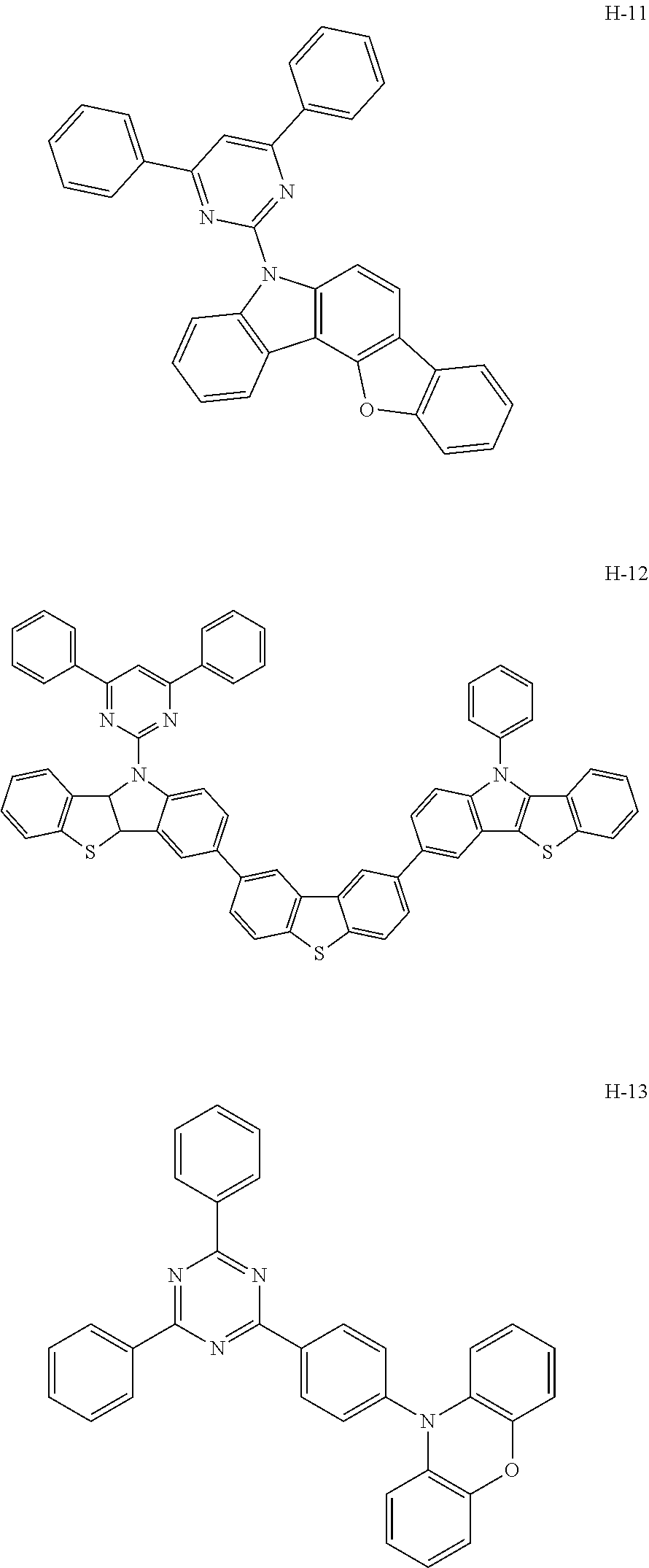


| TABLE 1 | ||||||
| HOMO | LUMO | ΔE | S1 | S1 | ||
| Compound | (eV) | (eV) | (eV) | (nm) | (eV) | f/S1 |
| Compound 11 | −4.68 | −3.00 | 1.67 | 864.7 | 1.43 | 0.54 |
| Compound 12 | −4.82 | −3.03 | 1.79 | 869.5 | 1.43 | 0.34 |
| Compound 19 | −4.80 | −3.13 | 1.67 | 865.6 | 1.43 | 0.74 |
| Compound 20 | −4.50 | −2.74 | 1.75 | 845.7 | 1.47 | 0.57 |
| Compound 30 | −4.98 | −3.42 | 1.56 | 985.5 | 1.26 | 0.02 |


| TABLE 2 | |||||
| Driving voltage (V) | EQE (%) | λMAX | |||
| Example 1 | 6.3 | 2.52 | 900 | ||
| Example 2 | 5.9 | 2.57 | 900 | ||
| Comparative | 7.9 | 0.50 | 968 | ||
| Example 1 | |||||
Claims (19)
D1-A-D2 Formula 1


D1-A-D2 Formula 1


D1-A-D2 Formula 1


Applications Claiming Priority (2)
| Application Number | Priority Date | Filing Date | Title |
|---|---|---|---|
| KR1020170122054A KR102431667B1 (en) | 2017-09-21 | 2017-09-21 | Heterocyclic compound, organic electroluminescence device and organic electroluminescence display device including the same |
| KR10-2017-0122054 | 2017-09-21 |
Publications (2)
| Publication Number | Publication Date |
|---|---|
| US20190084986A1 US20190084986A1 (en) | 2019-03-21 |
| US10844065B2 true US10844065B2 (en) | 2020-11-24 |
Family
ID=62951985
Family Applications (1)
| Application Number | Title | Priority Date | Filing Date |
|---|---|---|---|
| US15/963,036 Active 2039-03-13 US10844065B2 (en) | 2017-09-21 | 2018-04-25 | Heterocyclic compound, and organic electroluminescence device and organic electroluminescence display device including the same |
Country Status (4)
| Country | Link |
|---|---|
| US (1) | US10844065B2 (en) |
| EP (1) | EP3459946B1 (en) |
| KR (1) | KR102431667B1 (en) |
| CN (1) | CN109535160B (en) |
Families Citing this family (7)
| Publication number | Priority date | Publication date | Assignee | Title |
|---|---|---|---|---|
| KR102441825B1 (en) * | 2018-01-12 | 2022-09-07 | 주식회사 엘지화학 | Heterocyclic compound and organic photovoltaic device comprising the same |
| CN109535159B (en) * | 2018-12-17 | 2020-05-22 | 武汉华星光电半导体显示技术有限公司 | Red light thermal activation delay fluorescent material, preparation method thereof and organic light emitting diode device |
| KR102866754B1 (en) | 2019-03-04 | 2025-09-30 | 삼성디스플레이 주식회사 | Carrier, apparatus for manufacturing a display apparatus having the same and method for manufacturing a display apparatus |
| CN112951887A (en) | 2019-12-10 | 2021-06-11 | 三星显示有限公司 | Display device, mask assembly and apparatus for manufacturing display device |
| US11557635B2 (en) * | 2019-12-10 | 2023-01-17 | Samsung Display Co., Ltd. | Display device, mask assembly, and apparatus for manufacturing the display device |
| GB2591997A (en) * | 2020-02-04 | 2021-08-18 | Sumitomo Chemical Co | Photoactive material |
| CN119019405A (en) * | 2024-07-18 | 2024-11-26 | 深圳大学 | Aggregation-induced luminescence material with multiphoton absorption properties and preparation method and application thereof |
Citations (10)
| Publication number | Priority date | Publication date | Assignee | Title |
|---|---|---|---|---|
| US20070132372A1 (en) | 2005-11-28 | 2007-06-14 | Idemitsu Kosan Co., Ltd. | Amine based compound and organic electroluminescence device using the same |
| US20090153030A1 (en) * | 2007-12-14 | 2009-06-18 | Shouquan Huo | Oled device with substituted acridone compounds |
| CN102140083A (en) | 2010-01-29 | 2011-08-03 | 中国石油化学工业开发股份有限公司 | Novel quinoxaline derivative and organic light emitting diode device using the same |
| US8283052B2 (en) | 2006-09-29 | 2012-10-09 | Semiconductor Energy Laboratory Co., Ltd. | Quinoxaline derivative, light-emitting element, light-emitting device, and electronic appliance |
| US20160133856A1 (en) | 2014-11-12 | 2016-05-12 | Lg Display Co., Ltd. | Delayed fluorescence compound, and organic light emitting diode and display device using the same |
| KR20160056783A (en) | 2014-11-12 | 2016-05-20 | 엘지디스플레이 주식회사 | Delayed Fluorescence compound, and Organic light emitting diode device and Display device including the same |
| CN106047337A (en) | 2016-06-20 | 2016-10-26 | 武汉大学 | Quinoxaline unit containing organic thermally activated delayed fluorescent material and application thereof |
| KR101720079B1 (en) | 2015-03-31 | 2017-03-28 | (주)위델소재 | Quinoxaline derivative compound and organic electroluminescent device using the same |
| CN106831791A (en) * | 2017-03-06 | 2017-06-13 | 大连理工大学 | A class of ethylated pyrazinoquinoxaline derivatives and its preparation method |
| CN106967060A (en) | 2017-03-28 | 2017-07-21 | 石家庄诚志永华显示材料有限公司 | Serial carbazole derivates and application |
Family Cites Families (5)
| Publication number | Priority date | Publication date | Assignee | Title |
|---|---|---|---|---|
| JP5241183B2 (en) * | 2006-09-29 | 2013-07-17 | 株式会社半導体エネルギー研究所 | Quinoxaline derivative, light-emitting element, light-emitting device, and electronic device |
| CN101407493B (en) | 2008-05-29 | 2010-07-21 | 清华大学 | A kind of organic material and its application in organic electroluminescence device |
| KR101612903B1 (en) * | 2013-04-09 | 2016-04-19 | 희성소재 (주) | Phenazine-based compound and organic light emitting device comprising the same |
| CN104892579A (en) * | 2015-06-02 | 2015-09-09 | 吉林奥来德光电材料股份有限公司 | Aromatic heterocyclic compound and preparation method thereof, and organic electroluminescent device |
| CN107805243A (en) * | 2017-11-01 | 2018-03-16 | 长春海谱润斯科技有限公司 | A kind of derivative containing naphthazine structure and preparation method thereof and organic electroluminescence device |
-
2017
- 2017-09-21 KR KR1020170122054A patent/KR102431667B1/en active Active
-
2018
- 2018-04-25 US US15/963,036 patent/US10844065B2/en active Active
- 2018-07-13 EP EP18183515.8A patent/EP3459946B1/en active Active
- 2018-08-13 CN CN201810914570.XA patent/CN109535160B/en active Active
Patent Citations (13)
| Publication number | Priority date | Publication date | Assignee | Title |
|---|---|---|---|---|
| US20070132372A1 (en) | 2005-11-28 | 2007-06-14 | Idemitsu Kosan Co., Ltd. | Amine based compound and organic electroluminescence device using the same |
| KR20080080099A (en) | 2005-11-28 | 2008-09-02 | 이데미쓰 고산 가부시키가이샤 | Amine compound and organic electroluminescent device using same |
| US8283052B2 (en) | 2006-09-29 | 2012-10-09 | Semiconductor Energy Laboratory Co., Ltd. | Quinoxaline derivative, light-emitting element, light-emitting device, and electronic appliance |
| KR101426513B1 (en) | 2006-09-29 | 2014-08-05 | 가부시키가이샤 한도오따이 에네루기 켄큐쇼 | Quinoxaline derivatives, light emitting devices, light emitting devices and electronic devices |
| US20090153030A1 (en) * | 2007-12-14 | 2009-06-18 | Shouquan Huo | Oled device with substituted acridone compounds |
| CN102140083A (en) | 2010-01-29 | 2011-08-03 | 中国石油化学工业开发股份有限公司 | Novel quinoxaline derivative and organic light emitting diode device using the same |
| US20160133856A1 (en) | 2014-11-12 | 2016-05-12 | Lg Display Co., Ltd. | Delayed fluorescence compound, and organic light emitting diode and display device using the same |
| KR20160056783A (en) | 2014-11-12 | 2016-05-20 | 엘지디스플레이 주식회사 | Delayed Fluorescence compound, and Organic light emitting diode device and Display device including the same |
| KR101720079B1 (en) | 2015-03-31 | 2017-03-28 | (주)위델소재 | Quinoxaline derivative compound and organic electroluminescent device using the same |
| CN106047337A (en) | 2016-06-20 | 2016-10-26 | 武汉大学 | Quinoxaline unit containing organic thermally activated delayed fluorescent material and application thereof |
| CN106831791A (en) * | 2017-03-06 | 2017-06-13 | 大连理工大学 | A class of ethylated pyrazinoquinoxaline derivatives and its preparation method |
| CN106967060A (en) | 2017-03-28 | 2017-07-21 | 石家庄诚志永华显示材料有限公司 | Serial carbazole derivates and application |
| US20180282277A1 (en) | 2017-03-28 | 2018-10-04 | Shijiazhuang Chengzhi Yonghua Display Material Co.,Ltd. | Method for preparing a series of carbazole derivatives and use thereof in organic light-emitting diodes |
Non-Patent Citations (12)
| Title |
|---|
| English machine translation of Liu et al,, CN106831791A (Year: 2017). * |
| EPO Extended Search Report dated Mar. 18, 2019 for corresponding European Patent Application No. 18183515.8 (14 pages). |
| EPO Partial Search Report dated Nov. 14, 2018, for corresponding European Patent Application No. (10 pages). |
| Hedstrom, Svante, et al., "Light-harvesting capabilities of low band gap donor-acceptor polymers", Phys. Chem. Chem. Phys., 2014, vol. 16, (13 pages). |
| Lee, Po-I, et al., "New Conjugated Copolymers Based on Benzo [1,2-b; 3,4-b′] dithiophene and Derivatives of Benzo[g]quinoxaline for Bulk Heterojunction Solar Cells", Journal of Polymer Science: Part A: Polymar Chemistry, 2011, vol. 49, (9 pages). |
| Qin et al. "Multistimuli-Responsive Luminescence Switching of Pyrazine Derivative Based Donor-Acceptor-Donor Luminophores" Chem. Asian J. 2016, 11, 285-293. (Year: 2016). * |
| Qin et al. "Multistimuli-Responsive Luminescence Switching of Pyrazine Derivative Based Donor—Acceptor—Donor Luminophores" Chem. Asian J. 2016, 11, 285-293. (Year: 2016). * |
| Schulz, Gisela, et al., "Synthesis and Photovoltaic Performance of Pyrazinoquinoxaline Containing Conjugated Thiophene-Based Dendrimers and Polymers", Macromolecules, 2013, vol. 46, (11 pages). |
| Tam, Teck Lip Dexter, et al., "From benzobisthiadiazole, thiadiazoloquinoxaline to pyrazinoquinoxaline based polymers: effects of aromatic substituents on the performance of organic photovoltaics", Journal of Materials Chemistry, 2012, vol. 22, (7 pages). |
| Tam, Teck Lip, et al., "Substituent effect on the electronic properties of pyrazino[2, 3-g] quinoxaline molecules", Journal of Materials Chemistry, 2011, vol. 21, (7 pages). |
| Wang, Ergang, et al., Small Band Gap Polymers Synthesized via a Modified Nitration of 4,7-Dibromo-2,1,3-benzothiadiazole, Organic Letters, 2010, vol. 12, No. 20, (4 pages). |
| Zhang, Fengling, et al., "High Photovoltage achieved in low band gap polymer solar cells by adjusting energy levels of a polymer with the LUMOs of fullerence derivatives" Journal of Materials Chemistry, 2008, vol. 18, (7 pages). |
Also Published As
| Publication number | Publication date |
|---|---|
| CN109535160A (en) | 2019-03-29 |
| US20190084986A1 (en) | 2019-03-21 |
| CN109535160B (en) | 2023-04-14 |
| EP3459946B1 (en) | 2021-12-15 |
| KR20190033691A (en) | 2019-04-01 |
| EP3459946A2 (en) | 2019-03-27 |
| EP3459946A3 (en) | 2019-04-17 |
| KR102431667B1 (en) | 2022-08-12 |
Similar Documents
| Publication | Publication Date | Title |
|---|---|---|
| US10844065B2 (en) | Heterocyclic compound, and organic electroluminescence device and organic electroluminescence display device including the same | |
| US12538703B2 (en) | Organic electroluminescence device and electronic apparatus including the same | |
| KR102672246B1 (en) | Polycyclic compound and organic electroluminescence device including the same | |
| US20200176684A1 (en) | Organic electroluminescence device and polycyclic compound for organic electroluminescence device | |
| US11417843B2 (en) | Organic electroluminescence device and amine compound for organic electroluminescence device | |
| US20210098713A1 (en) | Organic electroluminescence device | |
| US10673000B2 (en) | Heterocyclic compound and organic electroluminescence device including the same | |
| US20210391540A1 (en) | Organic electroluminescence device and fused polycyclic compound for organic electroluminescence device | |
| US11018306B2 (en) | Compound for thermally activated delayed fluorescence and organic electroluminescence device including the same | |
| US10741774B2 (en) | Heterocyclic compound and organic electroluminescence device including the same | |
| KR20250084996A (en) | Heteroaryl amine derivatives and organic electroluminescent device including the same | |
| US20190097156A1 (en) | Silicon-containing compound and organic electroluminescence device including the same | |
| KR20220008985A (en) | Organic electroluminescent element and polycyclic compound for organic electroluminescent element | |
| US10862050B2 (en) | Heterocyclic compound and organic electroluminescence device including the same | |
| US11145829B2 (en) | Organic electroluminescent device, organic electroluminescent display device including the same, and organometallic compound for organic electroluminescent device | |
| KR102405140B1 (en) | Heterocyclic compound and organic electroluminescence device including the same | |
| KR102460493B1 (en) | Dibenzo five-membered ring compounds and organic electroluminescent device including the same | |
| US11569457B2 (en) | Organic electroluminescence device and polycyclic compound for organic electroluminescence device | |
| US20180020526A1 (en) | Organic electroluminescence device | |
| US20210288270A1 (en) | Organic electroluminescence device and organometallic compound for organic electroluminescence device | |
| US11335857B2 (en) | Organic electroluminescence device and display device including the same | |
| KR102701149B1 (en) | Organic electroluminescence device and fused polycyclic compound for organic electroluminescence device | |
| US10696697B2 (en) | Heterocyclic compound and organic electroluminescence device including the same | |
| KR20240128627A (en) | Tertiary amine derivatives and organic electroluminescent device comprising the same |
Legal Events
| Date | Code | Title | Description |
|---|---|---|---|
| FEPP | Fee payment procedure |
Free format text: ENTITY STATUS SET TO UNDISCOUNTED (ORIGINAL EVENT CODE: BIG.); ENTITY STATUS OF PATENT OWNER: LARGE ENTITY |
|
| AS | Assignment |
Owner name: SAMSUNG DISPLAY CO., LTD., KOREA, REPUBLIC OF Free format text: ASSIGNMENT OF ASSIGNORS INTEREST;ASSIGNORS:YE, JIMYOUNG;KIM, MYEONGSUK;KIM, SEULONG;AND OTHERS;SIGNING DATES FROM 20180228 TO 20180314;REEL/FRAME:045681/0401 |
|
| STPP | Information on status: patent application and granting procedure in general |
Free format text: DOCKETED NEW CASE - READY FOR EXAMINATION |
|
| STPP | Information on status: patent application and granting procedure in general |
Free format text: NON FINAL ACTION MAILED |
|
| STPP | Information on status: patent application and granting procedure in general |
Free format text: NOTICE OF ALLOWANCE MAILED -- APPLICATION RECEIVED IN OFFICE OF PUBLICATIONS |
|
| STPP | Information on status: patent application and granting procedure in general |
Free format text: PUBLICATIONS -- ISSUE FEE PAYMENT VERIFIED |
|
| STCF | Information on status: patent grant |
Free format text: PATENTED CASE |
|
| MAFP | Maintenance fee payment |
Free format text: PAYMENT OF MAINTENANCE FEE, 4TH YEAR, LARGE ENTITY (ORIGINAL EVENT CODE: M1551); ENTITY STATUS OF PATENT OWNER: LARGE ENTITY Year of fee payment: 4 |