US10840446B2 - Memory device - Google Patents
Memory device Download PDFInfo
- Publication number
- US10840446B2 US10840446B2 US16/287,753 US201916287753A US10840446B2 US 10840446 B2 US10840446 B2 US 10840446B2 US 201916287753 A US201916287753 A US 201916287753A US 10840446 B2 US10840446 B2 US 10840446B2
- Authority
- US
- United States
- Prior art keywords
- oxide layer
- metal oxide
- metal
- metal element
- memory device
- Prior art date
- Legal status (The legal status is an assumption and is not a legal conclusion. Google has not performed a legal analysis and makes no representation as to the accuracy of the status listed.)
- Active
Links
Images


Classifications
-
- H—ELECTRICITY
- H10—SEMICONDUCTOR DEVICES; ELECTRIC SOLID-STATE DEVICES NOT OTHERWISE PROVIDED FOR
- H10N—ELECTRIC SOLID-STATE DEVICES NOT OTHERWISE PROVIDED FOR
- H10N70/00—Solid-state devices having no potential barriers, and specially adapted for rectifying, amplifying, oscillating or switching
- H10N70/801—Constructional details of multistable switching devices
- H10N70/881—Switching materials
- H10N70/883—Oxides or nitrides
- H10N70/8836—Complex metal oxides, e.g. perovskites, spinels
-
- H—ELECTRICITY
- H10—SEMICONDUCTOR DEVICES; ELECTRIC SOLID-STATE DEVICES NOT OTHERWISE PROVIDED FOR
- H10B—ELECTRONIC MEMORY DEVICES
- H10B63/00—Resistance change memory devices, e.g. resistive RAM [ReRAM] devices
- H10B63/80—Arrangements comprising multiple bistable or multi-stable switching components of the same type on a plane parallel to the substrate, e.g. cross-point arrays
- H10B63/84—Arrangements comprising multiple bistable or multi-stable switching components of the same type on a plane parallel to the substrate, e.g. cross-point arrays arranged in a direction perpendicular to the substrate, e.g. 3D cell arrays
- H10B63/845—Arrangements comprising multiple bistable or multi-stable switching components of the same type on a plane parallel to the substrate, e.g. cross-point arrays arranged in a direction perpendicular to the substrate, e.g. 3D cell arrays the switching components being connected to a common vertical conductor
-
- H01L45/147—
-
- H01L27/2436—
-
- H01L27/249—
-
- H01L45/08—
-
- H01L45/1233—
-
- H01L45/146—
-
- H—ELECTRICITY
- H10—SEMICONDUCTOR DEVICES; ELECTRIC SOLID-STATE DEVICES NOT OTHERWISE PROVIDED FOR
- H10B—ELECTRONIC MEMORY DEVICES
- H10B63/00—Resistance change memory devices, e.g. resistive RAM [ReRAM] devices
- H10B63/30—Resistance change memory devices, e.g. resistive RAM [ReRAM] devices comprising selection components having three or more electrodes, e.g. transistors
-
- H—ELECTRICITY
- H10—SEMICONDUCTOR DEVICES; ELECTRIC SOLID-STATE DEVICES NOT OTHERWISE PROVIDED FOR
- H10N—ELECTRIC SOLID-STATE DEVICES NOT OTHERWISE PROVIDED FOR
- H10N70/00—Solid-state devices having no potential barriers, and specially adapted for rectifying, amplifying, oscillating or switching
- H10N70/20—Multistable switching devices, e.g. memristors
- H10N70/24—Multistable switching devices, e.g. memristors based on migration or redistribution of ionic species, e.g. anions, vacancies
-
- H—ELECTRICITY
- H10—SEMICONDUCTOR DEVICES; ELECTRIC SOLID-STATE DEVICES NOT OTHERWISE PROVIDED FOR
- H10N—ELECTRIC SOLID-STATE DEVICES NOT OTHERWISE PROVIDED FOR
- H10N70/00—Solid-state devices having no potential barriers, and specially adapted for rectifying, amplifying, oscillating or switching
- H10N70/801—Constructional details of multistable switching devices
- H10N70/821—Device geometry
- H10N70/826—Device geometry adapted for essentially vertical current flow, e.g. sandwich or pillar type devices
-
- H—ELECTRICITY
- H10—SEMICONDUCTOR DEVICES; ELECTRIC SOLID-STATE DEVICES NOT OTHERWISE PROVIDED FOR
- H10N—ELECTRIC SOLID-STATE DEVICES NOT OTHERWISE PROVIDED FOR
- H10N70/00—Solid-state devices having no potential barriers, and specially adapted for rectifying, amplifying, oscillating or switching
- H10N70/801—Constructional details of multistable switching devices
- H10N70/881—Switching materials
- H10N70/883—Oxides or nitrides
- H10N70/8833—Binary metal oxides, e.g. TaOx
Definitions
- Embodiments described herein relate generally to a memory device.
- a NAND flash memory has been spread as a memory device storing a large amount of data.
- a memory Cell has been scaled down to reduce costs per bit or to increase the amount of data stored in a memory device.
- a new memory device based on an operation principle different from that of a floating-gate flash memory is expected to be put to practical use.
- a variable resistance memory with two terminals which is typified by a resistive random access memory (ReRAM) promises to be a next-generation memory in terms of a low-voltage operation, a high-speed switching, and ease of scaling-down.
- ReRAM resistive random access memory
- variable resistance memory with two terminals is a variable resistance memory in which a variable resistance layer is made of metal oxide.
- a variable resistance layer is made of metal oxide.
- an electrical resistance value of metal oxide changes depending on the number of oxygen vacancies in a film. Therefore, a voltage is applied to metal oxide disposed between an upper electrode and a lower electrode to change the distribution of oxygen vacancies in the film. In this way, it is possible to switch the variable resistance layer between a high-resistance state and a low-resistance state.
- variable resistance memory has drawn attention which does not include a single metal oxide layer, but includes two or more metal oxide layers and has a function that is not obtained in a single-layer ReRAM.
- a stacked ReRAM obtained by stacking titanium oxide and aluminum oxide has self-compliance properties and two-dimensional conductivity and has drawn attention.
- a set voltage (Vset) required to reduce resistance is different from a reset voltage (Vreset) required to increase resistance. For this reason, in some cases, one of the voltages does not satisfy required voltage specifications. Therefore, it is preferable to adjust the balance between the set voltage and the reset voltage in the stacked ReRAM.
- FIG. 1 is a block diagram illustrating a memory device according to a first embodiment
- FIG. 2 is a cross-sectional view schematically illustrating a memory cell of the memory device according to the first embodiment
- FIG. 3 is a cross-sectional view schematically illustrating a memory cell of a memory device according to a comparative example
- FIGS. 4A and 4B are diagrams illustrating an operation principle of the memory cell according to the comparative example
- FIG. 5 is a cross-sectional view schematically illustrating a memory cell according to a second embodiment
- FIG. 6 is a cross-sectional view schematically illustrating a memory cell according to a third embodiment
- FIG. 7 is a cross-sectional view schematically illustrating a memory cell according to a fourth embodiment
- FIG. 8 is a cross-sectional view schematically illustrating a memory cell according to a fifth embodiment
- FIG. 9 is a cross-sectional view schematically illustrating a memory cell according to a sixth embodiment.
- FIG. 10 is a cross-sectional view schematically illustrating a memory cell according to a seventh embodiment
- FIG. 11 is a cross-sectional view schematically illustrating a memory cell according to an eighth embodiment.
- FIG. 12 is a cross-sectional view schematically illustrating a memory cell according to a ninth embodiment
- FIG. 13 is a cross-sectional view schematically illustrating a memory cell according to a tenth embodiment
- FIG. 14 is a cross-sectional view schematically illustrating a memory cell according to an eleventh embodiment
- FIG. 15 is a cross-sectional view schematically illustrating a memory cell according to a twelfth embodiment
- FIG. 16 is a cross-sectional view schematically illustrating a memory cell according to a thirteenth embodiment
- FIG. 17 is a cross-sectional view schematically illustrating a memory cell according to a fourteenth embodiment
- FIG. 18 is a cross-sectional view schematically illustrating a memory cell according to a fifteenth embodiment
- FIG. 19 is a cross-sectional view schematically illustrating a memory cell according to a sixteenth embodiment
- FIG. 20 is a cross-sectional view schematically illustrating a memory cell according to a seventeenth embodiment
- FIG. 21 is a cross-sectional view schematically illustrating a memory cell according to an eighteenth embodiment
- FIG. 22 is a cross-sectional view schematically illustrating a memory cell according to a nineteenth embodiment
- FIG. 23 is a cross-sectional view schematically illustrating a memory cell according to a twentieth embodiment
- FIG. 24 is a cross-sectional view schematically illustrating a memory cell according to a twenty-first embodiment
- FIG. 25 is a block diagram illustrating a memory device according to a twenty-second embodiment
- FIG. 26 is an equivalent circuit diagram illustrating a memory cell array according to the twenty-second embodiment.
- FIGS. 27A and 27B are cross-sectional views schematically illustrating the memory cell array according to the twenty-second embodiment.
- a memory device includes: a first conductive layer; a second conductive layer; a first metal oxide layer that is provided between the first conductive layer and the second conductive layer and includes at least one first metal element selected from the group consisting of aluminum (Al), gallium (Ga), zirconium (Zr), and hafnium (Hf); and a second metal oxide layer that is provided between the first metal oxide layer and the second conductive layer and includes at least one second metal element selected from the group consisting of zinc (Zn), titanium (Ti), tin (Sn), vanadium (V), niobium (Nb), tantalum (Ta), and tungsten (W).
- the first metal oxide layer includes a third metal element.
- the third metal element has a lower valence than a metal element having the highest atomic percent in the first metal oxide layer among the at least one first metal element.
- FIG. 1 is a block diagram illustrating a memory cell array 100 and peripheral circuits of the memory device according to this embodiment.
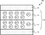
- FIG. 2 is a cross-sectional view schematically illustrating a memory cell MC of the memory device according to this embodiment.
- FIG. 2 illustrates, for example, the cross section of one memory cell MC which is represented by a dotted circle in the memory cell array 100 illustrated in FIG. 1 .
- the memory cell array 100 of the memory device includes, for example, a plurality of word lines 104 (first lines) and a plurality of bit lines 106 (second lines) intersecting the word lines 104 .
- the word lines 104 and the bit lines 106 are provided above the semiconductor substrate 101 , with an insulating layer interposed therebetween.
- the bit lines 106 are provided above the word lines 104 .
- a first control circuit 108 , a second control circuit 110 , and a sense circuit 112 are provided as the peripheral circuits around the memory cell array 100 .
- a plurality of memory cells MC are provided in regions in which the word lines 104 and the bit lines 106 intersect each other.
- the memory device according to this embodiment is a variable resistance memory having a cross-point structure.
- the memory cell MC is a variable resistance element with two terminals.
- Each of the plurality of word lines 104 is connected to the first control circuit 108 .
- each of the plurality of bit lines 106 is connected to the second control circuit 110 .
- the sense circuit 112 is connected to the first control circuit 108 and the second control circuit 110 .
- the first control circuit 108 and the second control circuit 110 have, for example, a function which selects a desired memory cell MC, writes data to the memory cell MC, reads data from the memory cell MC, and erases data in the memory cell MC.
- data in the memory cell is read as the amount of current flowing between the word line 104 and the bit line 106 .
- the sense circuit 112 has a function which determines the amount of current and determines the polarity of data. For example, the sense circuit 112 determines whether data is “0” or “1”.
- the first control circuit 108 , the second control circuit 110 , and the sense circuit 112 are, for example, electronic circuits Using semiconductor devices which are formed on the semiconductor substrate 101 .
- the memory cell MC includes a lower electrode 10 (first conductive layer), an upper electrode 20 (second conductive layer), and a variable resistance layer 30 .
- FIG. 2 illustrates an example of elements and oxygen vacancies included in the variable resistance layer 30 .
- the lower electrode 10 is connected to the word line 104 .
- the lower electrode 10 is made of, for example, metal.
- the lower electrode 10 is made of, for example, titanium (Ti), tungsten (W), tantalum (Ta), platinum (Pt), or an oxide thereof.
- the lower electrode 10 is made of, for example, titanium nitride.
- the lower electrode 10 may be a portion of the word line 104 .
- the upper electrode 20 is connected to the bit line 106 .
- the upper electrode 20 made of, for example, metal.
- the upper electrode 20 is made of, for example, titanium (Ti), tungsten (W), tantalum (Ta), platinum (Pt), or an oxide thereof.
- the upper electrode 20 is made of, for example, titanium nitride.
- the upper electrode 20 may be a portion of the bit line 106 .
- the variable resistance layer 30 is provided between the lower electrode 10 and the upper electrode 20 .
- the variable resistance layer 30 includes a first metal oxide layer 31 and a second metal oxide layer 32 .
- the thickness of the variable resistance layer 30 is, for example, equal to or greater than 1 nm and equal to or less than 40 nm.
- the first metal oxide layer 31 includes at least one first metal element selected from the group consisting of aluminum (Al), gallium (Ga), zirconium (Zr), and hafnium (Hf).
- the first metal oxide layer 31 has, for example, an oxide of the first metal element as a main component.
- the first metal oxide layer 31 is, for example, an aluminum oxide layer.
- the mole fraction of the oxide of the first metal element is higher than the mole fraction of each metal oxide other than the oxide of the first metal element in the first metal oxide layer 31 .
- the mole fraction of the oxide of the first metal element in the first metal oxide layer 31 is, for example, equal to or greater than 40%.
- the first metal element is a main metal element in the first metal oxide layer 31 .
- the atomic percent (atomic percentage) of the first metal element is the highest.
- the atomic percent of the first metal element among the metal elements is equal to or greater than 40%.
- the thickness of the first metal oxide layer 31 is, for example, equal to or greater than 0.5 nm and equal to or less than 10 nm.
- the second metal oxide layer 32 is provided between the first metal oxide layer 31 and the upper electrode 20 .
- the second metal oxide layer 32 includes at least one second metal element selected from the group consisting of zinc (Zn), titanium (Ti), tin (Sn), vanadium (V), niobium (Nb), tantalum (Ta), and tungsten (W).
- the second metal oxide layer 32 has, for example, an oxide of the second metal element as a main component.
- the second metal oxide layer 32 is, for example, a titanium oxide layer.
- the titanium oxide layer is, for example, an anatase titanium oxide layer.
- the mole fraction of the oxide of the second metal element is higher than the mole fraction of each metal oxide other than the oxide of the second metal element in the second metal oxide layer 32 .
- the mole fraction of the oxide of the second metal element in the second metal oxide layer 32 is, for example, equal to or greater than 40%.
- the second metal element is a main metal element in the second metal oxide layer 32 .
- the atomic percent of the second metal element is the highest.
- the atomic percent of the second metal element among the metal elements is equal to or greater than 40%.
- the oxide of the first metal element has a wider bandgap than the oxide of the second metal element.
- the oxide of the second metal element has semiconducting properties
- the oxide of the first metal element has insulating properties.
- the resistivity of the first metal oxide layer 31 is, for example, higher than the resistivity of the second metal oxide layer 32 .
- the thickness of the second metal oxide layer 32 is, for example, equal to or greater than 0.5 nm and equal to or less than 10 nm.
- the first metal oxide layer 31 includes a third metal element.
- the third metal element has a lower valence than the first metal element.
- the valence of the third metal element is compared with the valence of the first metal element having the highest atomic percent in the first metal oxide layer 31 .
- the third metal element is, for example, at least one metal element selected from the group consisting of aluminum (Al), gallium (Ga), zirconium (Zr), hafnium (Hf), zinc (Zn), titanium (Ti), tin (Sn), vanadium (V), niobium (Nb), tantalum (Ta), and tungsten (W).
- zinc (Zn) is a divalent (2+) element
- aluminum (Al) and gallium (Ga) are trivalent (3+) elements
- titanium (Ti), tin (Sn), zirconium (Zr), and hafnium (Hf) are tetravalent (4+) elements
- vanadium (V), niobium (Nb), and tantalum (Ta) are pentavalent (5+) elements
- tungsten is a hexavalent (6+) element.
- the atomic percent of the third metal element is lower than the atomic percent of the first metal element.
- the atomic percent of the third metal element is, for example, equal to or greater than 1 at % and equal to or less than 25 at %.
- the first metal element is trivalent aluminum (Al)
- the second metal element is tetravalent titanium (Ti)
- the third metal element is divalent zinc (Zn)
- the first metal oxide layer 31 is an aluminum oxide layer and the second metal oxide layer 32 is a titanium oxide layer.
- the aluminum oxide layer which is the first metal oxide layer 31 includes zinc (Zn). Zinc substitutes aluminum in the aluminum oxide layer.
- the identification of the kind of metal oxide included in the metal oxide layer or the measurement of the mole fractions of the metal oxides and the magnitude relationship between the mole fractions can be performed by, for example, X-ray photoemission spectroscopy (XPS) and an X-ray diffraction (XRD) method.
- XPS X-ray photoemission spectroscopy
- XRD X-ray diffraction
- the identification of the metal elements included in the metal oxide layer or the measurement of the atomic percent of the metal element and the magnitude relationship between the atomic percents can be performed by, for example, energy dispersive X-ray spectroscopy (EDX), an atom probe method, and electron energy loss spectroscopy (EELS).
- EDX energy dispersive X-ray spectroscopy
- EELS electron energy loss spectroscopy
- the lower electrode 10 an aluminum oxide layer which is the first metal oxide layer 31 , a titanium oxide layer which is the second metal oxide layer 32 , and the upper electrode 20 are formed in this order.
- the aluminum oxide layer and the titanium oxide layer are formed by, for example, a chemical vapor deposition method (CVD method), a sputtering method, or an atomic layer deposition method (ALD method).
- CVD method chemical vapor deposition method
- ALD method atomic layer deposition method
- the aluminum oxide layer is formed by the sputtering method
- zinc is added to the aluminum oxide layer using a sputtering target including zinc.
- a sputtering target including zinc for example, zinc is added to the aluminum oxide layer.
- FIG. 3 is a cross-sectional view schematically illustrating a memory cell of a memory device according to a comparative example.
- the memory cell includes a lower electrode 10 , an upper electrode 20 , and a variable resistance layer 30 .
- the variable resistance layer 30 includes a first metal oxide layer 31 and a second metal oxide layer 32 .
- the first metal oxide layer 31 is, for example, an aluminum oxide layer.
- the second metal oxide layer 32 is a titanium oxide layer.
- a memory cell MC according to the comparative example differs from the memory cell MC according to this embodiment except that the first metal oxide layer 31 does not include the third element.
- the aluminum oxide layer does not include zinc.
- FIGS. 4A and 4B are diagrams illustrating the operation principle of the memory cell according to the comparative example.
- the variable resistance layer 30 when a current is applied to the variable resistance layer 30 , the variable resistance layer 30 is changed from a high-resistance state to a low-resistance state or from a low-resistance state to a high-resistance state.
- the change from the high-resistance state to the low-resistance state is referred to as, for example, a set operation.
- the change from the low-resistance state to the high-resistance state is referred to as, for example, a reset operation.
- the high-resistance state is also referred to as an off state or a reset state.
- the low-resistance state is referred to as an on state or a set state. It is considered that the off state is changed to the on state by the following principle.
- oxygen vacancies are present in the titanium oxide layer which is the second metal oxide layer 32 .
- the following cases may be considered: a case in which the distribution of the oxygen vacancies in the titanium oxide layer is uniform; a case in which the oxygen vacancies are present only at the interface between the titanium oxide layer and the aluminum oxide layer which is the first metal oxide layer 31 ; and a case in which a filament is formed in the titanium oxide layer.
- variable resistance layer 30 has high resistance.
- a negative voltage applied to the lower electrode 10 a positive voltage is applied to the upper electrode 20 , and a set voltage (Vset) is applied between the lower electrode 10 and the upper electrode 20 . Then, an oxygen vacancy with positive charge is moved to the lower electrode 10 . In other words, oxygen with negative charge is moved to the upper electrode 20 .
- the oxygen vacancies in the titanium oxide layer disappear with the movement of the oxygen vacancies or the movement of oxygen and oxygen vacancies occur in the aluminum oxide layer which is the first metal oxide layer 31 .
- the following cases are considered: a case in which the distribution of the oxygen vacancies in the aluminum oxide layer is uniform; a case in which the oxygen vacancies are present only at the interface between the titanium oxide layer and the aluminum oxide layer; and a case in which a filament is formed in the aluminum oxide layer.
- the state illustrated in FIG. 4B is the on state.
- the resistance of the aluminum oxide layer which is the first metal oxide layer 31 is reduced and the variable resistance layer 30 has low resistance. It is considered that, since the second metal oxide layer 32 has a lower resistance than the first metal oxide layer 31 , a change in the resistance of the variable resistance layer 30 is dominated by a change in the resistance of the first metal oxide layer 31 .
- the on state illustrated in FIG. 4B is maintained even when the voltage drops to 0 V.
- a negative voltage is applied to the lower electrode 10
- a positive voltage is applied to the upper electrode 20
- a read voltage lower than the set voltage is applied to the memory cell MC in the on state
- a read current flows to the variable resistance layer 30 .
- a positive voltage is applied to the lower electrode 10
- a negative voltage is applied to the upper electrode 20
- a reset voltage (Vreset) is applied between the lower electrode 10 and the upper electrode 20 .
- an oxygen vacancy with positive charge is moved to the upper electrode 20 .
- oxygen with negative charge is moved to the lower electrode 10 . Therefore, the oxygen vacancies in the aluminum oxide layer which is the first metal oxide layer 31 disappear and the memory cell MC returns to the off state illustrated in FIG. 4A .
- the off state is defined as data “0” and the on state is defined as data “1”.
- the memory cell MC can store one set of data “0” and data “1”.
- the memory cell MC according to the comparative example has a vertically asymmetric layer structure. Therefore, in some cases, the set voltage which is an operating voltage required to reduce resistance is different from the reset voltage which is an operating voltage required to increase resistance. As a result, in some cases, one of the voltages does not satisfy the required voltage specifications. For this reason, a technique is required which adjusts the balance between the set voltage and the reset voltage in the memory cell MC according to the comparative example such that the required voltage specifications are satisfied.
- Both the set operation and the reset operation of the memory cell MC are the movement of oxygen between the first metal oxide layer 31 and the second metal oxide layer 32 . Therefore, it is considered that the set voltage and the reset voltage can be adjusted by controlling the oxygen affinity of the first metal oxide layer 31 or the second metal oxide layer 32 .
- an operation of reducing the oxygen affinity of the first metal oxide layer 31 is performed, an operation of increasing the oxygen affinity of the second metal oxide layer 32 is performed, or two operations are performed at the same time. In this case, it becomes easy for the oxygen to move from the first metal oxide layer 31 to the second metal oxide layer 32 . Therefore, the set voltage is reduced.
- the oxygen affinity of the metal oxide layer can be changed by controlling the amount of charge in the metal oxide layer.
- An oxygen ion is a divalent anion. Therefore, as the amount of positive charge in the metal oxide layer increases, the oxygen affinity increases. In contrast, as the amount of negative charge in the metal oxide layer increases, the oxygen affinity decreases.
- the amount of charge in the metal oxide layer is adjusted by adding an element to the metal oxide layer.
- the amount of charge in the metal oxide layer can be adjusted by adding an element with a different valence to substitute the metal element or oxygen in the metal oxide layer.
- the first metal oxide layer 31 includes the third metal element.
- the third metal element has a lower valence than the first metal element.
- divalent zinc (Zn) is included as the third metal element in the aluminum oxide layer which is the first metal oxide layer 31 .
- Zinc substitutes trivalent aluminum in the aluminum oxide layer.
- the amount of negative charge in the first metal oxide layer 31 increases.
- the oxygen affinity of the first metal oxide layer 31 is reduced.
- the set voltage is reduced.
- the first metal element is aluminum (Al) and the second metal element is titanium (Ti).
- the first metal oxide layer 31 is an aluminum oxide layer and the second metal oxide layer 32 is a titanium oxide layer.
- variable resistance layer 30 formed by combining the aluminum oxide layer and the titanium oxide layer makes it possible to achieve a stable on/off operation.
- the combination of the aluminum oxide layer and the titanium oxide layer has high affinity with a known semiconductor device manufacture process and makes it possible to achieve a memory device with high reliability at a low cost.
- the atomic percent of the first metal element among the metal elements is preferably equal to or greater than 40%, more preferably equal to or greater than 50%, and most preferably equal to or greater than 60%.
- the atomic percent of the second metal element among the metal elements is preferably equal to or greater than 40%, more preferably equal to or greater than 50%, and most preferably equal to or greater than 60%.
- the atomic percent of the third metal element among the metal elements included in the first metal oxide layer 31 is preferably equal to or greater than 1 at % and equal to or less than 25 at %.
- the atomic percent is less than the above-mentioned range, there is a concern that the operating voltage will not be adjusted.
- the atomic percent of the third metal element greater than the above-mentioned range is added, solid solubility exceeds the solid solubility limit of the first metal oxide layer 31 . As a result, there is a concern that a stable on/off operation will not be achieved.
- the oxygen affinity of metal oxide is controlled to achieve a variable resistance memory with an adjusted operating voltage.
- a memory device differs from the memory device according to the first embodiment in that the second metal oxide layer includes a third metal element and the third metal element has a lower valence than a metal element with the highest atomic percent in the second metal oxide layer among the at least one second metal element.
- the description of the same content as that in the first embodiment is not repeated.
- FIG. 5 is a cross-sectional view schematically illustrating a memory cell MC of the memory device according to this embodiment.
- a second metal oxide layer 32 includes the third metal element.
- the third metal element has a lower valence than the second metal element.
- the valence of the third metal element is compared with the valence of a second metal element with the highest atomic percent in the second metal oxide layer 32 .
- the third metal element is, for example, at least one metal element selected from the group consisting of aluminum (Al), gallium (Ga), zirconium (Zr), hafnium (Hf), zinc (Zn), titanium (Ti), tin (Sn), vanadium (V), niobium (Nb), tantalum (Ta), and tungsten (W).
- a first metal oxide layer 31 is an aluminum oxide layer and the second metal oxide layer 32 is a titanium oxide layer.
- the aluminum oxide layer and the titanium oxide layer are formed by, for example, a CVD method, a sputtering method, or an ALD method.
- titanium oxide layer is formed by the sputtering method
- aluminum is added to the titanium oxide layer using a sputtering target including aluminum.
- a titanium oxide film and an aluminum film are alternately stacked to add aluminum to the titanium oxide layer.
- the titanium oxide layer which is the second metal oxide layer 32 includes aluminum (Al). Trivalent aluminum substitutes tetravalent titanium in the titanium oxide layer.
- the amount of negative charge in the second metal oxide layer 32 increases.
- the oxygen affinity of the second metal oxide layer 32 is reduced.
- a reset voltage is reduced.
- variable resistance memory with an adjusted operating voltage is achieved.
- a memory device includes: a first conductive layer; a second conductive layer; a first metal oxide layer that is provided between the first conductive layer and the second conductive layer and includes at least one first metal element selected from the group consisting of aluminum (Al), gallium (Ga), zirconium (Zr), and hafnium (Hf); and a second metal oxide layer that is provided between the first metal oxide layer and the second conductive layer and includes at least one second metal element selected from the group consisting of zinc (Zn), titanium (Ti), tin (Sn), vanadium (V), niobium (Nb), tantalum (Ta), and tungsten (W).
- the first metal oxide layer includes a third metal element.
- the third metal element has a higher valence than a metal element having the highest atomic percent in the first metal oxide layer among the at least one first metal element.
- the memory device according to this embodiment differs from the memory device according to the first embodiment in that the third metal element has a higher valence than the first metal element.
- the description of the same content as that in the first embodiment is not repeated.
- FIG. 6 is a cross-sectional view schematically illustrating a memory cell MC of the memory device according to this embodiment.
- a first metal oxide layer 31 includes the third metal element.
- the third metal element has a higher valence than the first metal element.
- the third metal element is, for example, at least one metal element selected from the group consisting of aluminum (Al), gallium (Ga), zirconium (Zr), hafnium (Hf), zinc (Zn), titanium (Ti), tin (Sn), vanadium (V), niobium (Nb), tantalum (Ta), and tungsten (W).
- the first metal element is trivalent aluminum (Al)
- the second metal element is tetravalent titanium (Ti)
- the third metal element is pentavalent niobium (Nb)
- the first metal oxide layer 31 is an aluminum oxide layer and a second metal oxide layer 32 is a titanium oxide layer.
- the aluminum oxide layer which is the first metal oxide layer 31 includes niobium (Nb). Pentavalent niobium substitutes trivalent aluminum in the aluminum oxide layer.
- the amount of positive charge in the first metal oxide layer 31 increases.
- the oxygen affinity of the first metal oxide layer 31 increases.
- a reset voltage is reduced.
- variable resistance memory with an adjusted operating voltage is achieved.
- a memory device differs from the memory device according to the third embodiment in that the second metal oxide layer includes a third metal element and the third metal element has a higher valence than a metal element with the highest atomic percent in the second metal oxide layer among the at least one second metal element.
- the description of the same content as that in the third embodiment is not repeated.
- FIG. 7 is a cross-sectional view schematically illustrating a memory cell MC of the memory device according to this embodiment.
- a second metal oxide layer 32 includes a third metal element.
- the third metal element has a higher valence than the second metal element.
- the third metal element is, for example, at least one metal element selected from the group consisting of aluminum (Al), gallium (Ga), zirconium (Zr), hafnium (Hf), zinc (Zn), titanium (Ti), tin (Sn), vanadium (V), niobium (Nb), tantalum (Ta), and tungsten (W).
- a first metal oxide layer 31 is an aluminum oxide layer and the second metal oxide layer 32 is a titanium oxide layer.
- the titanium oxide layer which is the second metal oxide layer 32 includes tantalum (Ta). Pentavalent tantalum substitutes tetravalent titanium in the titanium oxide layer.
- the amount of positive charge in the second metal oxide layer 32 increases.
- the oxygen affinity of the second metal oxide layer 32 increases.
- a set voltage is reduced.
- variable resistance memory with an adjusted operating voltage is achieved.
- a memory device includes: a first conductive layer; a second conductive layer; a first metal oxide layer that is provided between the first conductive layer and the second conductive layer and includes a first metal element; and a second metal oxide layer that is provided between the first metal oxide layer and the second conductive layer and includes a second metal element different from the first metal element.
- the first metal oxide layer includes a halogen element.
- the memory device differs from the memory device according to the first embodiment in that the first metal oxide layer includes a halogen element.
- the description of the same content as that in the first embodiment is not repeated.
- FIG. 8 is a cross-sectional view schematically illustrating a memory cell MC of the memory device according to this embodiment.
- a first metal oxide layer 31 includes a halogen element.
- the halogen element is, for example, fluorine (F) or chlorine (Cl).
- the halogen element is a monovalent anion.
- the first metal element is trivalent aluminum (Al)
- the second metal element is tetravalent titanium (Ti)
- the halogen element is fluorine (F)
- the first metal oxide layer 31 is an aluminum oxide layer and a second metal oxide layer 32 is a titanium oxide layer.
- the aluminum oxide layer and the titanium oxide layer are formed by, for example, a CVD method, a sputtering method, or an ALD method.
- fluorine is added to the aluminum oxide layer by ion implantation.
- the atomic percent of the halogen element is lower than the atomic percent of oxygen.
- the atomic percent of the halogen element is, for example, equal to or greater than 1 at % and equal to or less than 25 at %.
- the aluminum oxide layer which is the first metal oxide layer 31 includes fluorine (F).
- F fluorine
- Monovalent fluorine substitutes divalent oxygen in the aluminum oxide layer.
- the amount of positive charge in the first metal oxide layer 31 increases.
- the oxygen affinity of the first metal oxide layer 31 increases.
- a reset voltage is reduced.
- variable resistance memory with an adjusted operating voltage is achieved.
- a memory device differs from the memory device according to the fifth embodiment in that the second metal oxide layer includes a halogen element.
- the description of the same content as that in the fifth embodiment is not repeated.
- FIG. 9 is a cross-sectional view schematically illustrating a memory cell MC of the memory device according to this embodiment.
- a second metal oxide layer 32 includes a halogen element.
- the halogen element is, for example, fluorine (F) or chlorine (Cl).
- the halogen element is a monovalent anion.
- a first metal oxide layer 31 is an aluminum oxide layer and the second metal oxide layer 32 is a titanium oxide layer.
- the aluminum oxide layer and the titanium oxide layer are formed by, for example, a CVD method, a sputtering method, or an ALD method.
- fluorine is added to the titanium oxide layer by ion implantation.
- the atomic percent of the halogen element is lower than the atomic percent of oxygen.
- the atomic percent of the halogen element is, for example, equal to or greater than 1 at % and equal to or less than 25 at %.
- the titanium oxide layer which is the second metal oxide layer 32 includes fluorine (F).
- F fluorine
- Monovalent fluorine substitutes divalent oxygen in the titanium oxide layer.
- the amount of positive charge in the second metal oxide layer 32 increases.
- the oxygen affinity of the second metal oxide layer 32 increases.
- a set voltage is reduced.
- variable resistance memory with an adjusted operating voltage is achieved.
- a memory device includes: a first conductive layer; a second conductive layer; a first metal oxide layer that is provided between the first conductive layer and the second conductive layer and includes a first metal element; and a second metal oxide layer that is provided between the first metal oxide layer and the second conductive layer and includes a second metal element different from the first metal element.
- the first metal oxide layer includes at least one element selected from the group consisting of nitrogen (N), phosphorus (P), and arsenic (As).
- the memory device differs from the memory device according to the first embodiment in that the first metal oxide layer includes at least one element selected from the group consisting of nitrogen (N), phosphorus (P), and arsenic (As).
- N nitrogen
- P phosphorus
- As arsenic
- FIG. 10 is a cross-sectional view schematically illustrating a memory cell MC of the memory device according to this embodiment.
- a first metal oxide layer 31 includes at least one element selected from the group consisting of nitrogen (N), phosphorus (P), and arsenic (As). Nitrogen (N), phosphorus (P), and arsenic (As) are trivalent anions.
- the first metal element is trivalent aluminum (Al)
- the second metal element is tetravalent titanium (Ti)
- at least one element selected from the group consisting of nitrogen (N), phosphorus (P), and arsenic (As) is nitrogen (N) will be described.
- the first metal oxide layer 31 is an aluminum oxide layer and a second metal oxide layer 32 is a titanium oxide layer.
- the aluminum oxide layer and the titanium oxide layer are formed by, for example, a CVD method, a sputtering method, or an ALD method.
- nitrogen is added to the aluminum oxide layer by ion implantation.
- the atomic percent of the at least one element selected from the group consisting of nitrogen (N), phosphorus (P), and arsenic (As) is lower than the atomic percent of oxygen.
- the atomic percent of the at least one element selected from the group consisting of nitrogen (N), phosphorus (P), and arsenic (As) is, for example, equal to or greater than 1 at % and equal to or less than 25 at %.
- the aluminum oxide layer which is the first metal oxide layer 31 includes nitrogen (N). Trivalent nitrogen substitutes divalent oxygen in the aluminum oxide layer.
- the amount of negative charge in the first metal oxide layer 31 increases.
- the oxygen affinity of the first metal oxide layer 31 is reduced.
- a set voltage is reduced.
- variable resistance memory with an adjusted operating voltage is achieved.
- a memory device differs from the memory device according to the seventh embodiment in that the second metal oxide layer includes at least one element selected from the group consisting of nitrogen (N), phosphorus (P), and arsenic (As).
- N nitrogen
- P phosphorus
- As arsenic
- FIG. 11 is a cross-sectional view schematically illustrating a memory cell MC of the memory device according to this embodiment.
- a second metal oxide layer 32 includes at least one element selected from the group consisting of nitrogen (N), phosphorus (P), and arsenic (As). Nitrogen (N), phosphorus (P), and arsenic (As) are trivalent anions.
- the first metal element is trivalent aluminum (Al)
- the second metal element is tetravalent titanium (Ti)
- at least one element selected from the group consisting of nitrogen (N), phosphorus (P), and arsenic (As) is nitrogen (N) will be described.
- a first metal oxide layer 31 is an aluminum oxide layer and the second metal oxide layer 32 is a titanium oxide layer.
- the aluminum oxide layer and the titanium oxide layer are formed by, for example, a CVD method, a sputtering method, or an ALD method.
- nitrogen is added to the titanium oxide layer by ion implantation.
- the atomic percent of the at least one element selected from the group consisting of nitrogen (N), phosphorus (P), and arsenic (As) is lower than the atomic percent of oxygen.
- the atomic percent of the at least one element selected from the group consisting of nitrogen (N), phosphorus (P), and arsenic (As) is, for example, equal to or greater than 1 at % and equal to or less than 25 at %.
- the titanium oxide layer which is the second metal oxide layer 32 includes nitrogen (N). Trivalent nitrogen substitutes divalent oxygen in the titanium oxide layer.
- the amount of negative charge in the second metal oxide layer 32 increases.
- the oxygen affinity of the second metal oxide layer 32 is reduced.
- a reset voltage is reduced.
- variable resistance memory with an adjusted operating voltage is achieved.
- a memory device differs from the memory device according to the first embodiment in that the second metal oxide layer includes a fourth metal element having a higher valence than the second metal element.
- the description of the same content as that in the first embodiment is not repeated.
- FIG. 12 is a cross-sectional view schematically illustrating a memory cell MC of the memory device according to this embodiment.
- a first metal oxide layer 31 includes a third metal element.
- the third metal element has a lower valence than the first metal element.
- the third metal element is, for example, at least one metal element selected from the group consisting of aluminum (Al), gallium (Ga), zirconium (Zr), hafnium (Hf), zinc (Zn), titanium (Ti), tin (Sn), vanadium (V), niobium (Nb), tantalum (Ta), and tungsten (W).
- a second metal oxide layer 32 includes a fourth metal element.
- the fourth metal element has a higher valence than the second metal element.
- the fourth metal element is at least one metal element selected from the group consisting of aluminum (Al), gallium (Ga), zirconium (Zr), hafnium (Hf), zinc (Zn), titanium (Ti), tin (Sn), vanadium (V), niobium (Nb), tantalum (Ta), and tungsten (W).
- the first metal element is trivalent aluminum (Al)
- the second metal element is tetravalent titanium (Ti)
- the third metal element is divalent zinc (Zn)
- the fourth metal element is pentavalent tantalum (Ta)
- the first metal oxide layer 31 is an aluminum oxide layer and the second metal oxide layer 32 is a titanium oxide layer.
- the aluminum oxide layer which is the first metal oxide layer 31 includes zinc (Zn). Divalent zinc substitutes trivalent aluminum in the aluminum oxide layer. In addition, pentavalent tantalum substitutes tetravalent titanium in the titanium oxide layer which is the second metal oxide layer 32 .
- the amount of negative charge in the first metal oxide layer 31 increases.
- the oxygen affinity of the first metal oxide layer 31 is reduced.
- the amount of positive charge in the second metal oxide layer 32 increases. Therefore, the oxygen affinity of the second metal oxide layer 32 increases.
- a set voltage is significantly reduced by the synergy of both.
- variable resistance memory with an adjusted operating voltage is achieved.
- the adjustment range of the operating voltage is widened.
- a memory device differs from the memory device according to the second embodiment in that the first metal oxide layer includes a fourth metal element having a higher valence than the first metal element.
- the description of the same content as that in the second embodiment is not repeated.
- FIG. 13 is a cross-sectional view schematically illustrating a memory cell MC of the memory device according to this embodiment.
- a second metal oxide layer 32 includes a third metal element.
- the third metal element has a lower valence than the first metal element.
- the third metal element is, for example, at least one metal element selected from the group consisting of aluminum (Al), gallium (Ga), zirconium (Zr), hafnium (Hf), zinc (Zn), titanium (Ti), tin (Sn), vanadium (V), niobium (Nb), tantalum (Ta), and tungsten (W).
- a first metal oxide layer 31 includes a fourth metal element.
- the fourth metal element has a higher valence than the first metal element.
- the fourth metal element is at least one metal element selected from the group consisting of aluminum (Al), gallium (Ga), zirconium (Zr), hafnium (Hf), zinc (Zn), titanium (Ti), tin (Sn), vanadium (V), niobium (Nb), tantalum (Ta), and tungsten (W).
- the first metal element is trivalent aluminum (Al)
- the second metal element is tetravalent titanium (Ti)
- the third metal element is trivalent aluminum (Al)
- the fourth metal element is pentavalent niobium (Nb)
- the first metal oxide layer 31 is an aluminum oxide layer and the second metal oxide layer 32 is a titanium oxide layer.
- the aluminum oxide layer which is the first metal oxide layer 31 includes niobium (Nb). Pentavalent niobium substitutes trivalent aluminum in the aluminum oxide layer. In addition, trivalent aluminum substitutes tetravalent titanium in the titanium oxide layer which is the second metal oxide layer 32 .
- the amount of positive charge in the first metal oxide layer 31 increases.
- the oxygen affinity of the first metal oxide layer 31 increases.
- the amount of positive charge in the second metal oxide layer 32 is reduced. Therefore, the oxygen affinity of the second metal oxide layer 32 is reduced.
- a reset voltage is significantly reduced by the synergy of both.
- variable resistance memory with an adjusted operating voltage is achieved.
- the adjustment range of the operating voltage is widened.
- a memory device differs from the memory device according to the first embodiment in that the first metal oxide layer includes at least one element selected from the group consisting of nitrogen (N), phosphorus (P), and arsenic (As).
- N nitrogen
- P phosphorus
- As arsenic
- FIG. 14 is a cross-sectional view schematically illustrating a memory cell MC of the memory device according to this embodiment.
- a first metal oxide layer 31 includes a third metal element.
- the third metal element has a lower valence than the first metal element.
- the third metal element is, for example, at least one metal element selected from the group consisting of aluminum (Al), gallium (Ga), zirconium (Zr), hafnium (Hf), zinc (Zn), titanium (Ti), tin (Sn), vanadium (V), niobium (Nb), tantalum (Ta), and tungsten (W).
- the first metal oxide layer 31 includes at least one element selected from the group consisting of nitrogen (N), phosphorus (P), and arsenic (As). Nitrogen (N), phosphorus (P), and arsenic (As) are trivalent anions.
- the first metal element is trivalent aluminum (Al)
- the second metal element is tetravalent titanium (Ti)
- the third metal element is divalent zinc (Zn)
- at least one element selected from the group consisting of nitrogen (N), phosphorus (P), and arsenic (As) is nitrogen (N) will be described.
- the first metal oxide layer 31 is an aluminum oxide layer and a second metal oxide layer 32 is a titanium oxide layer.
- the aluminum oxide layer which is the first metal oxide layer 31 includes zinc (Zn).
- Divalent niobium substitutes trivalent aluminum in the aluminum oxide layer.
- trivalent nitrogen substitutes divalent oxygen in the aluminum oxide layer which is the first metal oxide layer 31 .
- the amount of negative charge in the first metal oxide layer 31 increases significantly.
- the oxygen affinity of the first metal oxide layer 31 is significantly reduced.
- a set voltage is significantly reduced.
- variable resistance memory with an adjusted operating voltage is achieved.
- the adjustment range of the operating voltage is widened.
- a memory device differs from the memory device according to the first embodiment in that the second metal oxide layer includes a halogen element.
- the description of the same content as that in the first embodiment is not repeated.
- FIG. 15 is a cross-sectional view schematically illustrating a memory cell MC of the memory device according to this embodiment.
- a first metal oxide layer 31 includes a third metal element.
- the third metal element has a lower valence than the first metal element.
- the third metal element is, for example, at least one metal element selected from the group consisting of aluminum (Al), gallium (Ga), zirconium (Zr), hafnium (Hf), zinc (Zn), titanium (Ti), tin (Sn), vanadium (V), niobium (Nb), tantalum (Ta), and tungsten (W).
- a second metal oxide layer 32 includes a halogen element.
- the halogen element is, for example, fluorine (F) or chlorine (Cl).
- the halogen element is a monovalent anion.
- the first metal element is trivalent aluminum (Al)
- the second metal element is tetravalent titanium (Ti)
- the third metal element is divalent zinc (Zn)
- the halogen element is fluorine (F)
- the first metal oxide layer 31 is an aluminum oxide layer and the second metal oxide layer 32 is a titanium oxide layer.
- the aluminum oxide layer which is the first metal oxide layer 31 includes zinc (Zn).
- Divalent zinc substitutes trivalent aluminum in the aluminum oxide layer.
- monovalent fluorine substitutes divalent oxygen in the titanium oxide layer which is the second metal oxide layer 32 .
- the amount of negative charge in the first metal oxide layer 31 increases.
- the oxygen affinity of the first metal oxide layer 31 is reduced.
- the amount of positive charge in the second metal oxide layer 32 increases. Therefore, the oxygen affinity of the second metal oxide layer 32 increases.
- a set voltage is significantly reduced by the synergy of both.
- variable resistance memory with an adjusted operating voltage is achieved.
- the adjustment range of the operating voltage is widened.
- a memory device differs from the memory device according to the second embodiment in that the first metal oxide layer includes a halogen element.
- the description of the same content as that in the second embodiment is not repeated.
- FIG. 16 is a cross-sectional view schematically illustrating a memory cell MC of the memory device according to this embodiment.
- a second metal oxide layer 32 includes a third metal element.
- the third metal element has a lower valence than the first metal element.
- the third metal element is, for example, at least one metal element selected from the group consisting of aluminum (Al), gallium (Ga), zirconium (Zr), hafnium (Hf), zinc (Zn), titanium (Ti), tin (Sn), vanadium (V), niobium (Nb), tantalum (Ta), and tungsten (W).
- a first metal oxide layer 31 includes a halogen element.
- the halogen element is, for example, fluorine (F) or chlorine (Cl).
- the halogen element is a monovalent anion.
- the first metal element is trivalent aluminum (Al)
- the second metal element is tetravalent titanium (Ti)
- the third metal element is trivalent aluminum (Al)
- the halogen element is fluorine (F)
- the first metal oxide layer 31 is an aluminum oxide layer and the second metal oxide layer 32 is a titanium oxide layer.
- the aluminum oxide layer which is the first metal oxide layer 31 includes fluorine (F).
- F fluorine
- Monovalent fluorine substitutes divalent oxygen in the aluminum oxide layer.
- trivalent aluminum substitutes tetravalent titanium in the titanium oxide layer which is the second metal oxide layer 32 .
- the amount of positive charge in the first metal oxide layer 31 increases.
- the oxygen affinity of the first metal oxide layer 31 increases.
- the amount of positive charge in the second metal oxide layer 32 is reduced. Therefore, the oxygen affinity of the second metal oxide layer 32 is reduced.
- a reset voltage is significantly reduced by the synergy of both.
- variable resistance memory with an adjusted operating voltage achieved.
- the adjustment range of the operating voltage is widened.
- a memory device differs from the memory device according to the second embodiment in that the second metal oxide layer includes at least one element selected from the group consisting of nitrogen (N), phosphorus (P), and arsenic (As).
- N nitrogen
- P phosphorus
- As arsenic
- FIG. 17 is a cross-sectional view schematically illustrating a memory cell MC of the memory device according to this embodiment.
- a second metal oxide layer 32 includes a third metal element.
- the third metal element has a lower valence than the first metal element.
- the third metal element is, for example, at least one metal element selected from the group consisting of aluminum (Al), gallium (Ga), zirconium (Zr), hafnium (Hf), zinc (Zn), titanium (Ti), tin (Sn), vanadium (V), niobium (Nb), tantalum (Ta), and tungsten (W).
- the second metal oxide layer 32 includes at least one element selected from the group consisting of nitrogen (N), phosphorus (P), and arsenic (As). Nitrogen (N), phosphorus (P), and arsenic (As) are trivalent anions.
- a first metal oxide layer 31 is an aluminum oxide layer and the second metal oxide layer 32 is a titanium oxide layer.
- trivalent aluminum substitutes tetravalent titanium in the titanium oxide layer which is the second metal oxide layer 32 .
- trivalent nitrogen substitutes divalent oxygen in the titanium oxide layer which is the second metal oxide layer 32 .
- the amount of negative charge in the second metal oxide layer 32 increases significantly.
- the oxygen affinity of the second metal oxide layer 32 is significantly reduced.
- a reset voltage is significantly reduced by the synergy of both.
- variable resistance memory with an adjusted operating voltage is achieved.
- the adjustment range of the operating voltage is widened.
- a memory device differs from the memory device according to the third embodiment in that the first metal oxide layer includes a halogen element.
- the description of the same content as that in the third embodiment is not repeated.
- FIG. 18 is a cross-sectional view schematically illustrating a memory cell MC of the memory device according to this embodiment.
- a first metal oxide layer 31 includes a third metal element.
- the third metal element has a higher valence than the first metal element.
- the third metal element is, for example, at least one metal element selected from the group consisting of aluminum (Al), gallium (Ga), zirconium (Zr), hafnium (Hf), zinc (Zn), titanium (Ti), tin (Sn), vanadium (V), niobium (Nb), tantalum (Ta), and tungsten (W).
- the first metal oxide layer 31 includes a halogen element.
- the halogen element is, for example, fluorine (F) or chlorine (Cl).
- the halogen element is a monovalent anion.
- the first metal element is trivalent aluminum (Al)
- the second metal element is tetravalent titanium (Ti)
- the third metal element is pentavalent niobium
- the halogen element is fluorine (F)
- the first metal oxide layer 31 is an aluminum oxide layer and a second metal oxide layer 32 is a titanium oxide layer.
- the aluminum oxide layer which is the first metal oxide layer 31 includes niobium (Nb). Pentavalent niobium substitutes trivalent aluminum in the aluminum oxide layer. In addition, the aluminum oxide layer which is the first metal oxide layer 31 includes fluorine (F). Monovalent niobium substitutes divalent oxygen in the aluminum oxide layer.
- the amount of positive charge in the first metal oxide layer 31 increases significantly.
- the oxygen affinity of the first metal oxide layer 31 increases significantly.
- a reset voltage is reduced.
- variable resistance memory with an adjusted operating voltage is achieved.
- the adjustment range of the operating voltage is widened.
- a memory device differs from the memory device according to the third embodiment in that the second metal oxide layer includes at least one element selected from the group consisting of nitrogen (N), phosphorus (P), and arsenic (As).
- N nitrogen
- P phosphorus
- As arsenic
- FIG. 19 is a cross-sectional view schematically illustrating a memory cell MC of the memory device according to this embodiment.
- a first metal oxide layer 31 includes a third metal element.
- the third metal element has a higher valence than the first metal element.
- the third metal element is, for example, at least one metal element selected from the group consisting of aluminum (Al), gallium (Ga), zirconium (Zr), hafnium (Hf), zinc (Zn), titanium (Ti), tin (Sn), vanadium (V), niobium (Nb), tantalum (Ta), and tungsten (W).
- a second metal oxide layer 32 includes at least one element selected from the group consisting of nitrogen (N), phosphorus (P), and arsenic (As). Nitrogen (N), phosphorus (P), and arsenic (As) are trivalent anions.
- the first metal element is trivalent aluminum (Al)
- the second metal element is tetravalent titanium (Ti)
- the third metal element is pentavalent niobium (Nb)
- at least one element selected from the group consisting of nitrogen (N), phosphorus (P), and arsenic (As) is nitrogen (N) will be described.
- a first metal oxide layer 31 is an aluminum oxide layer and the second metal oxide layer 32 is a titanium oxide layer.
- the aluminum oxide layer which is the first metal oxide layer 31 includes niobium (Nb). Pentavalent niobium substitutes trivalent aluminum in the aluminum oxide layer. In addition, trivalent nitrogen substitutes divalent oxygen in the titanium oxide layer which is the second metal oxide layer 32 .
- the amount of positive charge in the first metal oxide layer 31 increases.
- the oxygen affinity of the first metal oxide layer 31 increases.
- the amount of negative charge in the second metal oxide layer 32 increases. Therefore, the oxygen affinity of the second metal oxide layer 32 is reduced.
- a reset voltage is significantly reduced by the synergy of both.
- variable resistance memory with an adjusted operating voltage is achieved.
- the adjustment range of the operating voltage is widened.
- a memory device differs from the memory device according to the fourth embodiment in that the first metal oxide layer includes at least one element selected from the group consisting of nitrogen (N), phosphorus (P), and arsenic (As).
- N nitrogen
- P phosphorus
- As arsenic
- FIG. 20 is a cross-sectional view schematically illustrating a memory cell MC of the memory device according to this embodiment.
- a second metal oxide layer 32 includes a third metal element.
- the third metal element has a higher valence than the second metal element.
- the third metal element is, for example, at least one metal element selected from the group consisting of aluminum (Al), gallium (Ga), zirconium (Zr), hafnium (Hf), zinc (Zn), titanium (Ti), tin (Sn), vanadium (V), niobium (Nb), tantalum (Ta), and tungsten (W).
- a first metal oxide layer 31 includes at least one element selected from the group consisting of nitrogen (N), phosphorus (P), and arsenic (As). Nitrogen (N), phosphorus (P), and arsenic (As) are trivalent anions.
- the first metal element is trivalent aluminum (Al)
- the second metal element is tetravalent titanium (Ti)
- the third metal element is pentavalent tantalum (Ta)
- at least one element selected from the group consisting of nitrogen (N), phosphorus (P), and arsenic (As) is nitrogen (N) will be described.
- the first metal oxide layer 31 is an aluminum oxide layer and the second metal oxide layer 32 is a titanium oxide layer.
- the titanium oxide layer which is the second metal oxide layer 32 includes tantalum (Ta). Pentavalent tantalum substitutes tetravalent titanium in the titanium oxide layer.
- the aluminum oxide layer which is the first metal oxide layer 31 includes nitrogen (N). Trivalent nitrogen substitutes divalent oxygen in the aluminum oxide layer.
- the amount of negative charge in the first metal oxide layer 31 increases.
- the oxygen affinity of the first metal oxide layer 31 is reduced.
- the amount of positive charge in the second metal oxide layer 32 increases. Therefore, the oxygen affinity of the second metal oxide layer 32 increases.
- a set voltage is significantly reduced by the synergy of both.
- variable resistance memory with an adjusted operating voltage is achieved.
- the adjustment range of the operating voltage is widened.
- a memory device differs from the memory device according to the fourth embodiment in that the second metal oxide layer includes a halogen element.
- the description of the same content as that in the fourth embodiment is not repeated.
- FIG. 21 is a cross-sectional view schematically illustrating a memory cell MC of the memory device according to this embodiment.
- a second metal oxide layer 32 includes a third metal element.
- the third metal element has a higher valence than the second metal element.
- the third metal element is, for example, at least one metal element selected from the group consisting of aluminum (Al), gallium (Ga), zirconium (Zr), hafnium (Hf), zinc (Zn), titanium (Ti), tin (Sn), vanadium (V), niobium (Nb), tantalum (Ta), and tungsten (W).
- the second metal oxide layer 32 includes a halogen element.
- the halogen element is, for example, fluorine (F) or chlorine (Cl).
- the halogen element is a monovalent anion.
- a first metal oxide layer 31 is an aluminum oxide layer and the second metal oxide layer 32 is a titanium oxide layer.
- the titanium oxide layer which is the second metal oxide layer 32 includes tantalum (Ta).
- Pentavalent tantalum substitutes tetravalent titanium in the titanium oxide layer.
- monovalent fluorine substitutes divalent oxygen in the titanium oxide layer which is the second metal oxide layer 32 .
- the amount of positive charge in the second metal oxide layer 32 increases significantly.
- the oxygen affinity of the second metal oxide layer 32 increases significantly.
- a reset voltage is significantly reduced.
- variable resistance memory with an adjusted operating voltage is achieved.
- the adjustment range of the operating voltage is widened.
- a memory device differs from the memory device according to the fifth embodiment in that the second metal oxide layer includes at least one element selected from the group consisting of nitrogen (N), phosphorus (P), and arsenic (As).
- N nitrogen
- P phosphorus
- As arsenic
- FIG. 22 is a cross-sectional view schematically illustrating a memory cell MC of the memory device according to this embodiment.
- a first metal oxide layer 31 includes a halogen element.
- the halogen element is, for example, fluorine (F) or chlorine (Cl).
- the halogen element is a monovalent anion.
- a second metal oxide layer 32 includes at least one element selected from the group consisting of nitrogen (N), phosphorus (P), and arsenic (As). Nitrogen (N), phosphorus (P), and arsenic (As) are trivalent anions.
- the first metal element is trivalent aluminum (Al)
- the second metal element is tetravalent titanium (Ti)
- the halogen element is fluorine (F)
- at least one element selected from the group consisting of nitrogen (N), phosphorus (P), and arsenic (As) is nitrogen (N) will be described.
- the first metal oxide layer 31 is an aluminum oxide layer and the second metal oxide layer 32 is a titanium oxide layer.
- the aluminum oxide layer which is the first metal oxide layer 31 includes fluorine (F). Monovalent fluorine substitutes divalent oxygen in the aluminum oxide layer.
- the titanium oxide layer which is the second metal oxide layer 32 includes nitrogen (N). Trivalent nitrogen substitutes divalent oxygen in the titanium oxide layer.
- variable resistance memory with an adjusted operating voltage is achieved.
- the adjustment range of the operating voltage is widened.
- a memory device differs from the memory device according to the sixth embodiment in that the first metal oxide layer includes at least one element selected from the group consisting of nitrogen (N), phosphorus (P), and arsenic (As).
- N nitrogen
- P phosphorus
- As arsenic
- FIG. 23 is a cross-sectional view schematically illustrating a memory cell MC of the memory device according to this embodiment.
- a second metal oxide layer 32 includes a halogen element.
- the halogen element is, for example, fluorine (F) or chlorine (Cl).
- the halogen element is a monovalent anion.
- a first metal oxide layer 31 includes at least one element selected from the group consisting of nitrogen (N), phosphorus (P), and arsenic (As). Nitrogen (N), phosphorus (P), and arsenic (As) are trivalent anions.
- the first metal element is trivalent aluminum (Al)
- the second metal element is tetravalent titanium (Ti)
- the halogen element is fluorine (F)
- at least one element selected from the group consisting of nitrogen (N), phosphorus (P), and arsenic (As) is nitrogen (N) will be described.
- the first metal oxide layer 31 is an aluminum oxide layer and the second metal oxide layer 32 is a titanium oxide layer.
- the titanium oxide layer which is the second metal oxide layer 32 includes fluorine (F). Monovalent fluorine substitutes divalent oxygen in the titanium oxide layer.
- the aluminum oxide layer which is the first metal oxide layer 31 includes nitrogen (N). Trivalent nitrogen substitutes divalent oxygen in the aluminum oxide layer.
- the amount of negative charge in the first metal oxide layer 31 increases.
- the oxygen affinity of the first metal oxide layer 31 is reduced.
- the amount of positive charge in the second metal oxide layer 32 increases. Therefore, the oxygen affinity of the second metal oxide layer 32 is reduced.
- a set voltage is significantly reduced by the synergy of both.
- variable resistance memory with an adjusted operating voltage is achieved.
- the adjustment range of the operating voltage is widened.
- a memory device differs from the memory devices according to the first to twentieth embodiments in that it further includes an amorphous silicon layer provided between the first conductive layer and the first metal oxide layer.
- an amorphous silicon layer provided between the first conductive layer and the first metal oxide layer.
- FIG. 24 is a cross-sectional view schematically illustrating a memory cell MC of the memory device according to this embodiment.
- the memory cell MC includes a lower electrode 10 (first conductive layer), an upper electrode 20 (second conductive layer), a variable resistance layer 30 , and an amorphous silicon layer 40 .
- the amorphous silicon layer 40 is provided between the lower electrode 10 and the variable resistance layer 30 .
- amorphous silicon means silicon of which the crystal grains are not observed from an image magnified a hundred thousand times by a transmission electron microscope (TEM).
- variable resistance memory of this embodiment a variation in the current that flows to the memory cell MC is prevented. Therefore, it is possible to achieve a variable resistance memory with a stable operation in addition to the effects of the first to twentieth embodiments.
- a memory device differs from the memory devices according to the first to twenty-first embodiments in that the memory cell array has a three-dimensional structure. Therefore, the description of the same content as that in the first to twenty-first embodiments will not be repeated.
- FIG. 25 is a block diagram illustrating the memory device according to this embodiment.
- FIG. 26 is an equivalent circuit diagram illustrating a memory cell array.
- FIGS. 27A and 27B are cross-sectional views schematically illustrating the memory cell array.
- the memory cell array according to this embodiment has a three-dimensional structure in which memory cells MC are three-dimensionally disposed.
- the memory device includes a memory cell array 200 , a word line driver circuit 212 , a row decoder circuit 214 , a sense amplifier circuit 215 , a column decoder circuit 217 , and a control circuit 221 .
- a plurality of memory cells MC are three-dimensionally disposed in the memory cell array 200 .
- a region surrounded by a dashed line corresponds to one memory cell MC.
- the memory cell array 200 includes, for example, a plurality of word lines WL (WL 11 , WL 12 , WL 13 , WL 21 , WL 22 , and WL 23 ) (first lines) and a plurality of bit lines BL (BL 11 , BL 12 , BL 21 , and BL 22 ) (second lines).
- the word line WL extends in the x direction.
- the bit line BL extends in the z direction.
- the word line WL and the bit line BL perpendicularly intersect each other.
- the memory cell MC is disposed in an intersection portion between the word line WL and the bit line BL.
- the plurality of word lines WL are electrically connected to the row decoder circuit 214 .
- the plurality of bit lines BL are connected to the sense amplifier circuit 215 .
- Select transistors ST (ST 11 , ST 21 , ST 12 , and ST 22 ) and global bit lines GBL (GBL 1 and GBL 2 ) are provided between the plurality of bit lines BL and the sense amplifier circuit 215 .
- the row decoder circuit 214 has a function which selects the word line WL on the basis of an input row address signal.
- the word line driver circuit 212 has a function which applies a predetermined voltage to the word line WL selected by the row decoder circuit 214 .
- the column decoder circuit 217 has a function which selects the bit line BL on the basis of an input column address signal.
- the sense amplifier circuit 215 has a function which applies a predetermined voltage to the bit line BL selected by the column decoder circuit 217 .
- the sense amplifier circuit 215 has a function which detects the current flowing between the selected word line WL and the selected bit line BL and amplifies the current.
- the control circuit 221 has a function which controls the word line driver circuit 212 , the row decoder circuit 214 , the sense amplifier circuit 215 , the column decoder circuit 217 , and other circuits (not illustrated).
- Circuits such as the word line driver circuit 212 , the row decoder circuit 214 , the sense amplifier circuit 215 , the column decoder circuit 217 , and the control circuit 221 , are formed by, for example, transistors using semiconductor layers (not illustrated) or wiring layers.
- FIGS. 27A and 27B are cross-sectional views schematically illustrating the memory cell array 200 of the memory device according to this embodiment.
- FIG. 27A is an xy cross-sectional view illustrating the memory cell array 200 .
- FIG. 27B is a yz cross-sectional view illustrating the memory cell array 200 .
- FIG. 27A is a cross-sectional view taken along the line BB′ of FIG. 27B and
- FIG. 27B is a cross-sectional view taken along the line AA′ of FIG. 27A .
- a region surrounded b a dashed line corresponds to one memory cell MC.
- the memory cell array 200 includes the word line WL 11 , the word line WL 12 , the word line WL 13 , the bit line BL 11 , and the bit line BL 12 .
- the memory cell array 200 includes a variable resistance layer 30 and an interlayer insulating layer 50 .
- the variable resistance layer 30 according to one of the first to twenty-first embodiments may be applied to the variable resistance layer 30 .
- the memory device since the memory device has a three-dimensional structure, it is possible to obtain the effect of improving the degree of integration of the memory device, in addition to the effects of the first to twenty-first embodiments.
- a memory device comprising:
- first metal oxide layer provided between the first conductive layer and the second conductive layer, the first metal oxide layer including a first metal element
- the second metal oxide layer including a second metal element different from the first metal element
- the first metal oxide layer includes a halogen element.
- the second metal oxide layer includes at least one element Selected from the group consisting of nitrogen (N), phosphorus (P), and arsenic (As).
- a memory device comprising:
- first metal oxide layer provided between the first conductive layer and the second conductive layer, the first metal oxide layer including a first metal element
- the second metal oxide layer including a second metal element different from the first metal element
- the second metal oxide layer includes a halogen element.
- the first metal oxide layer includes at least one element selected from the group consisting of nitrogen (N), phosphorus (P), and arsenic (As).
- a memory device comprising:
- first metal oxide layer provided between the first conductive layer and the second conductive layer, the first metal oxide layer including a first metal element
- the second metal oxide layer including a second metal element different from the first metal element
- the second metal oxide layer includes at least one element selected from the group consisting of nitrogen (N), phosphorus (P), and arsenic (As).
- the first metal element is at least one metal element selected from the group consisting of aluminum (Al), gallium (Ga), zirconium (Zr), and hafnium (Hf), and
- the second metal element is at least one metal element selected from the group consisting of zinc (Zn), titanium (Ti), tin (Sn), vanadium (V), niobium (Nb), tantalum (Ta), and tungsten (W).
- a memory device comprising:
- first metal oxide layer provided between the first conductive layer and the second conductive layer, the first metal oxide layer including at least one first metal element selected from the group consisting of aluminum (Al), gallium (Ga), zirconium (Zr), and hafnium (Hf);
- the second metal oxide layer including at least one second metal element selected from the group consisting of zinc (Zn), titanium (Ti), tin (Sn), vanadium (V), niobium (Nb), tantalum (Ta), and tungsten (W); and
- the first metal oxide layer includes a third metal element
- the third metal element has a lower valence than a metal element having the highest atomic percent in the first metal oxide layer among the at least one first metal element.
Landscapes
- Chemical & Material Sciences (AREA)
- Engineering & Computer Science (AREA)
- Materials Engineering (AREA)
- Semiconductor Memories (AREA)
Abstract
Description
Claims (20)
Priority Applications (1)
| Application Number | Priority Date | Filing Date | Title |
|---|---|---|---|
| US16/287,753 US10840446B2 (en) | 2017-03-22 | 2019-02-27 | Memory device |
Applications Claiming Priority (4)
| Application Number | Priority Date | Filing Date | Title |
|---|---|---|---|
| JP2017056696A JP2018160547A (en) | 2017-03-22 | 2017-03-22 | Storage device |
| JP2017-056696 | 2017-03-22 | ||
| US15/709,753 US10256404B2 (en) | 2017-03-22 | 2017-09-20 | Memory device |
| US16/287,753 US10840446B2 (en) | 2017-03-22 | 2019-02-27 | Memory device |
Related Parent Applications (1)
| Application Number | Title | Priority Date | Filing Date |
|---|---|---|---|
| US15/709,753 Continuation US10256404B2 (en) | 2017-03-22 | 2017-09-20 | Memory device |
Publications (2)
| Publication Number | Publication Date |
|---|---|
| US20190198760A1 US20190198760A1 (en) | 2019-06-27 |
| US10840446B2 true US10840446B2 (en) | 2020-11-17 |
Family
ID=63581905
Family Applications (2)
| Application Number | Title | Priority Date | Filing Date |
|---|---|---|---|
| US15/709,753 Active US10256404B2 (en) | 2017-03-22 | 2017-09-20 | Memory device |
| US16/287,753 Active US10840446B2 (en) | 2017-03-22 | 2019-02-27 | Memory device |
Family Applications Before (1)
| Application Number | Title | Priority Date | Filing Date |
|---|---|---|---|
| US15/709,753 Active US10256404B2 (en) | 2017-03-22 | 2017-09-20 | Memory device |
Country Status (3)
| Country | Link |
|---|---|
| US (2) | US10256404B2 (en) |
| JP (1) | JP2018160547A (en) |
| TW (1) | TWI664757B (en) |
Families Citing this family (5)
| Publication number | Priority date | Publication date | Assignee | Title |
|---|---|---|---|---|
| JP2019057661A (en) * | 2017-09-22 | 2019-04-11 | 東芝メモリ株式会社 | Semiconductor storage |
| KR102722302B1 (en) * | 2019-06-12 | 2024-10-24 | 어플라이드 머티어리얼스, 인코포레이티드 | Dual oxide analog switches for neuromorphic switching |
| KR102796866B1 (en) * | 2019-12-27 | 2025-04-17 | 삼성전자주식회사 | Variable resistance memory device |
| US11430951B2 (en) | 2020-04-24 | 2022-08-30 | Taiwan Semiconductor Manufacturing Company, Ltd. | Resistive memory cell with switching layer comprising one or more dopants |
| KR102359393B1 (en) * | 2020-08-14 | 2022-02-08 | 건국대학교 산학협력단 | Filament-based device with low variation switching voltage implemented using leakage current characteristics in oxide double layers and manufacturing method thereof |
Citations (10)
| Publication number | Priority date | Publication date | Assignee | Title |
|---|---|---|---|---|
| JPS5436603B2 (en) | 1972-12-29 | 1979-11-10 | ||
| JPS5547111B2 (en) | 1978-03-22 | 1980-11-27 | ||
| JP2008243913A (en) | 2007-03-26 | 2008-10-09 | Kanagawa Acad Of Sci & Technol | Variable resistance element and memory element |
| US20090039336A1 (en) | 2007-08-08 | 2009-02-12 | Hitachi, Ltd. | Semiconductor device |
| TW200906328A (en) | 2007-08-03 | 2009-02-16 | shi-yu Shen | Impact-resistant shoesole |
| JP2010267930A (en) | 2009-05-18 | 2010-11-25 | Toshiba Corp | Method for manufacturing nonvolatile memory device |
| US8437173B2 (en) | 2010-03-19 | 2013-05-07 | Panasonic Corporation | Nonvolatile memory element, manufacturing method thereof, design support method therefor, and nonvolatile memory device |
| US8698277B2 (en) | 2011-02-15 | 2014-04-15 | Kabushiki Kaisha Toshiba | Nonvolatile variable resistance device having metal halogen or metal sulfide layer |
| US20140210835A1 (en) * | 2013-01-25 | 2014-07-31 | Qualcomm Mems Technologies, Inc. | Metal oxide layer composition control by atomic layer deposition for thin film transistor |
| JP5696260B2 (en) | 2012-09-05 | 2015-04-08 | 株式会社アルバック | Resistance change element and manufacturing method thereof |
-
2017
- 2017-03-22 JP JP2017056696A patent/JP2018160547A/en active Pending
- 2017-09-20 US US15/709,753 patent/US10256404B2/en active Active
- 2017-09-21 TW TW106132363A patent/TWI664757B/en active
-
2019
- 2019-02-27 US US16/287,753 patent/US10840446B2/en active Active
Patent Citations (13)
| Publication number | Priority date | Publication date | Assignee | Title |
|---|---|---|---|---|
| JPS5436603B2 (en) | 1972-12-29 | 1979-11-10 | ||
| JPS5547111B2 (en) | 1978-03-22 | 1980-11-27 | ||
| JP2008243913A (en) | 2007-03-26 | 2008-10-09 | Kanagawa Acad Of Sci & Technol | Variable resistance element and memory element |
| TW200906328A (en) | 2007-08-03 | 2009-02-16 | shi-yu Shen | Impact-resistant shoesole |
| US20090039336A1 (en) | 2007-08-08 | 2009-02-12 | Hitachi, Ltd. | Semiconductor device |
| JP2010267930A (en) | 2009-05-18 | 2010-11-25 | Toshiba Corp | Method for manufacturing nonvolatile memory device |
| US8437173B2 (en) | 2010-03-19 | 2013-05-07 | Panasonic Corporation | Nonvolatile memory element, manufacturing method thereof, design support method therefor, and nonvolatile memory device |
| JP5436603B2 (en) | 2010-03-19 | 2014-03-05 | パナソニック株式会社 | Nonvolatile memory element and nonvolatile memory device |
| US8698277B2 (en) | 2011-02-15 | 2014-04-15 | Kabushiki Kaisha Toshiba | Nonvolatile variable resistance device having metal halogen or metal sulfide layer |
| JP5547111B2 (en) | 2011-02-15 | 2014-07-09 | 株式会社東芝 | Nonvolatile resistance change element and method of manufacturing nonvolatile resistance change element |
| JP5696260B2 (en) | 2012-09-05 | 2015-04-08 | 株式会社アルバック | Resistance change element and manufacturing method thereof |
| US9343207B2 (en) | 2012-09-05 | 2016-05-17 | Ulvac, Inc. | Resistance change device, and method for producing same |
| US20140210835A1 (en) * | 2013-01-25 | 2014-07-31 | Qualcomm Mems Technologies, Inc. | Metal oxide layer composition control by atomic layer deposition for thin film transistor |
Non-Patent Citations (1)
| Title |
|---|
| B. Govoreanu, et al. "Vacancy-Modulated Conductive Oxide Resistive RAM (VMCO-RRAM): An Area-Scalable Switching Current, Self-Compliant, Highly Nonlinear and Wide On/Off-Window Resistive Switching Cell," 2013, IEDM13, pp. 256-259. |
Also Published As
| Publication number | Publication date |
|---|---|
| JP2018160547A (en) | 2018-10-11 |
| US20180277759A1 (en) | 2018-09-27 |
| US10256404B2 (en) | 2019-04-09 |
| US20190198760A1 (en) | 2019-06-27 |
| TWI664757B (en) | 2019-07-01 |
| TW201843854A (en) | 2018-12-16 |
Similar Documents
| Publication | Publication Date | Title |
|---|---|---|
| US10840446B2 (en) | Memory device | |
| US11462685B2 (en) | Switch device, storage apparatus, and memory system incorporating boron and carbon | |
| US10529777B2 (en) | Switch device and storage unit | |
| US8031510B2 (en) | Ion barrier cap | |
| KR102297252B1 (en) | Switch element and memory device | |
| US8981332B2 (en) | Nonvolatile resistive memory element with an oxygen-gettering layer | |
| US20210036221A1 (en) | Switching device and storage unit, and memory system | |
| CN102782846B (en) | Non-volatile memory element and non-volatile memory device equipped with same | |
| US20130128654A1 (en) | Nonvolatile memory element, method of manufacturing nonvolatile memory element, method of initial breakdown of nonvolatile memory element, and nonvolatile memory device | |
| US11522132B2 (en) | Storage device and storage unit with a chalcogen element | |
| US10147874B2 (en) | Memory device | |
| US10892300B2 (en) | Storage device | |
| US12507423B2 (en) | Memory device and conductive layer | |
| US9105332B2 (en) | Variable resistance nonvolatile memory device | |
| JP6433860B2 (en) | Storage device | |
| US9735201B2 (en) | Memory device | |
| US10158067B2 (en) | Memory device | |
| US20190088715A1 (en) | Memory device | |
| CN113228254B (en) | Resistance variable nonvolatile memory element and resistance variable nonvolatile memory device using same |
Legal Events
| Date | Code | Title | Description |
|---|---|---|---|
| FEPP | Fee payment procedure |
Free format text: ENTITY STATUS SET TO UNDISCOUNTED (ORIGINAL EVENT CODE: BIG.); ENTITY STATUS OF PATENT OWNER: LARGE ENTITY |
|
| STPP | Information on status: patent application and granting procedure in general |
Free format text: NON FINAL ACTION MAILED |
|
| STPP | Information on status: patent application and granting procedure in general |
Free format text: RESPONSE TO NON-FINAL OFFICE ACTION ENTERED AND FORWARDED TO EXAMINER |
|
| STPP | Information on status: patent application and granting procedure in general |
Free format text: NON FINAL ACTION MAILED |
|
| STPP | Information on status: patent application and granting procedure in general |
Free format text: NOTICE OF ALLOWANCE MAILED -- APPLICATION RECEIVED IN OFFICE OF PUBLICATIONS |
|
| STPP | Information on status: patent application and granting procedure in general |
Free format text: PUBLICATIONS -- ISSUE FEE PAYMENT RECEIVED |
|
| STCF | Information on status: patent grant |
Free format text: PATENTED CASE |
|
| AS | Assignment |
Owner name: K.K PANGEA, JAPAN Free format text: MERGER;ASSIGNOR:TOSHIBA MEMORY CORPORATION;REEL/FRAME:058946/0675 Effective date: 20180801 Owner name: KIOXIA CORPORATION, JAPAN Free format text: CHANGE OF NAME AND ADDRESS;ASSIGNOR:TOSHIBA MEMORY CORPORATION;REEL/FRAME:058905/0582 Effective date: 20191001 |
|
| AS | Assignment |
Owner name: TOSHIBA MEMORY CORPORATION, JAPAN Free format text: CHANGE OF NAME AND ADDRESS;ASSIGNOR:K.K PANGEA;REEL/FRAME:058957/0124 Effective date: 20180801 |
|
| MAFP | Maintenance fee payment |
Free format text: PAYMENT OF MAINTENANCE FEE, 4TH YEAR, LARGE ENTITY (ORIGINAL EVENT CODE: M1551); ENTITY STATUS OF PATENT OWNER: LARGE ENTITY Year of fee payment: 4 |