US10838318B2 - Optical scanning apparatus and image forming apparatus - Google Patents
Optical scanning apparatus and image forming apparatus Download PDFInfo
- Publication number
- US10838318B2 US10838318B2 US16/373,499 US201916373499A US10838318B2 US 10838318 B2 US10838318 B2 US 10838318B2 US 201916373499 A US201916373499 A US 201916373499A US 10838318 B2 US10838318 B2 US 10838318B2
- Authority
- US
- United States
- Prior art keywords
- substrate
- laser light
- detection unit
- deflector
- light source
- Prior art date
- Legal status (The legal status is an assumption and is not a legal conclusion. Google has not performed a legal analysis and makes no representation as to the accuracy of the status listed.)
- Expired - Fee Related
Links
- 230000003287 optical effect Effects 0.000 title claims abstract description 106
- 239000000758 substrate Substances 0.000 claims abstract description 98
- 238000001514 detection method Methods 0.000 claims abstract description 40
- 239000004065 semiconductor Substances 0.000 description 18
- 238000000034 method Methods 0.000 description 8
- 230000000052 comparative effect Effects 0.000 description 6
- 230000001276 controlling effect Effects 0.000 description 5
- 229910000679 solder Inorganic materials 0.000 description 5
- 239000006071 cream Substances 0.000 description 4
- 230000008569 process Effects 0.000 description 4
- 238000005476 soldering Methods 0.000 description 4
- 230000015572 biosynthetic process Effects 0.000 description 3
- 239000011347 resin Substances 0.000 description 3
- 229920005989 resin Polymers 0.000 description 3
- RYGMFSIKBFXOCR-UHFFFAOYSA-N Copper Chemical compound [Cu] RYGMFSIKBFXOCR-UHFFFAOYSA-N 0.000 description 2
- 229910052802 copper Inorganic materials 0.000 description 2
- 239000010949 copper Substances 0.000 description 2
- 230000008054 signal transmission Effects 0.000 description 2
- 239000000654 additive Substances 0.000 description 1
- 230000000996 additive effect Effects 0.000 description 1
- 230000008901 benefit Effects 0.000 description 1
- 230000008859 change Effects 0.000 description 1
- 238000009826 distribution Methods 0.000 description 1
- 230000000694 effects Effects 0.000 description 1
- 239000000945 filler Substances 0.000 description 1
- 230000004907 flux Effects 0.000 description 1
- 239000003365 glass fiber Substances 0.000 description 1
- 238000010438 heat treatment Methods 0.000 description 1
- 238000001746 injection moulding Methods 0.000 description 1
- 238000004519 manufacturing process Methods 0.000 description 1
- 239000000463 material Substances 0.000 description 1
- 239000000155 melt Substances 0.000 description 1
- 238000002844 melting Methods 0.000 description 1
- 230000008018 melting Effects 0.000 description 1
- 238000012986 modification Methods 0.000 description 1
- 230000004048 modification Effects 0.000 description 1
- 238000003825 pressing Methods 0.000 description 1
- 230000001105 regulatory effect Effects 0.000 description 1
- 230000000452 restraining effect Effects 0.000 description 1
- 230000000630 rising effect Effects 0.000 description 1
- 238000009751 slip forming Methods 0.000 description 1
- 239000012780 transparent material Substances 0.000 description 1
Images


Classifications
-
- G—PHYSICS
- G03—PHOTOGRAPHY; CINEMATOGRAPHY; ANALOGOUS TECHNIQUES USING WAVES OTHER THAN OPTICAL WAVES; ELECTROGRAPHY; HOLOGRAPHY
- G03G—ELECTROGRAPHY; ELECTROPHOTOGRAPHY; MAGNETOGRAPHY
- G03G15/00—Apparatus for electrographic processes using a charge pattern
- G03G15/04—Apparatus for electrographic processes using a charge pattern for exposing, i.e. imagewise exposure by optically projecting the original image on a photoconductive recording material
- G03G15/043—Apparatus for electrographic processes using a charge pattern for exposing, i.e. imagewise exposure by optically projecting the original image on a photoconductive recording material with means for controlling illumination or exposure
-
- G—PHYSICS
- G02—OPTICS
- G02B—OPTICAL ELEMENTS, SYSTEMS OR APPARATUS
- G02B26/00—Optical devices or arrangements for the control of light using movable or deformable optical elements
- G02B26/08—Optical devices or arrangements for the control of light using movable or deformable optical elements for controlling the direction of light
- G02B26/0816—Optical devices or arrangements for the control of light using movable or deformable optical elements for controlling the direction of light by means of one or more reflecting elements
-
- G—PHYSICS
- G02—OPTICS
- G02B—OPTICAL ELEMENTS, SYSTEMS OR APPARATUS
- G02B26/00—Optical devices or arrangements for the control of light using movable or deformable optical elements
- G02B26/08—Optical devices or arrangements for the control of light using movable or deformable optical elements for controlling the direction of light
- G02B26/10—Scanning systems
- G02B26/12—Scanning systems using multifaceted mirrors
- G02B26/124—Details of the optical system between the light source and the polygonal mirror
-
- G—PHYSICS
- G02—OPTICS
- G02B—OPTICAL ELEMENTS, SYSTEMS OR APPARATUS
- G02B26/00—Optical devices or arrangements for the control of light using movable or deformable optical elements
- G02B26/08—Optical devices or arrangements for the control of light using movable or deformable optical elements for controlling the direction of light
- G02B26/10—Scanning systems
- G02B26/12—Scanning systems using multifaceted mirrors
- G02B26/127—Adaptive control of the scanning light beam, e.g. using the feedback from one or more detectors
-
- G—PHYSICS
- G03—PHOTOGRAPHY; CINEMATOGRAPHY; ANALOGOUS TECHNIQUES USING WAVES OTHER THAN OPTICAL WAVES; ELECTROGRAPHY; HOLOGRAPHY
- G03G—ELECTROGRAPHY; ELECTROPHOTOGRAPHY; MAGNETOGRAPHY
- G03G21/00—Arrangements not provided for by groups G03G13/00 - G03G19/00, e.g. cleaning, elimination of residual charge
- G03G21/16—Mechanical means for facilitating the maintenance of the apparatus, e.g. modular arrangements
- G03G21/1661—Mechanical means for facilitating the maintenance of the apparatus, e.g. modular arrangements means for handling parts of the apparatus in the apparatus
- G03G21/1666—Mechanical means for facilitating the maintenance of the apparatus, e.g. modular arrangements means for handling parts of the apparatus in the apparatus for the exposure unit
-
- G—PHYSICS
- G02—OPTICS
- G02B—OPTICAL ELEMENTS, SYSTEMS OR APPARATUS
- G02B27/00—Optical systems or apparatus not provided for by any of the groups G02B1/00 - G02B26/00, G02B30/00
- G02B27/0025—Optical systems or apparatus not provided for by any of the groups G02B1/00 - G02B26/00, G02B30/00 for optical correction, e.g. distorsion, aberration
- G02B27/0031—Optical systems or apparatus not provided for by any of the groups G02B1/00 - G02B26/00, G02B30/00 for optical correction, e.g. distorsion, aberration for scanning purposes
-
- G—PHYSICS
- G02—OPTICS
- G02B—OPTICAL ELEMENTS, SYSTEMS OR APPARATUS
- G02B27/00—Optical systems or apparatus not provided for by any of the groups G02B1/00 - G02B26/00, G02B30/00
- G02B27/30—Collimators
Definitions
- the present disclosure relates to an image forming apparatus such as a copying machine, printer, and facsimile machine, and to an optical scanning apparatus used for the image forming apparatus.
- An optical scanning apparatus used for an image forming apparatus such as a copying machine, printer, and facsimile machine optically modulates laser light emitted from a light source based on an image signal, and deflects the optically modulated laser light for scanning by using, for example, a deflector having a rotating polygon mirror.
- the deflected laser light for scanning is focused on the surface of a photosensitive drum by a scanning lens such as f ⁇ lens to form an electrostatic latent image.
- a development device supplies a developer to the electrostatic latent image formed on the surface of the photosensitive drum to develop the electrostatic latent image into a visualized toner image.
- the toner image is transferred onto a recording medium such as paper which is then sent to a fixing device.
- the fixing device heats the toner image on the recording medium to fix the toner image thereto, thus accomplishing printing.
- the optical scanning apparatus deflects the laser light emitted from the light source and performs scanning, by using a deflector having a rotating polygon mirror.
- the optical scanning apparatus controls the position for starting image writing by the laser light reflected by reflection surfaces of the rotating polygon mirror. More specifically, the optical scanning apparatus controls the irradiation position to be irradiated with the laser light, of the photosensitive drum. Therefore, the optical scanning apparatus includes a substrate mounting a beam detect (BD) sensor as a detection unit for receiving laser light and generating a horizontal synchronization signal for controlling the irradiation position to be irradiated with the laser light.
- BD beam detect
- the horizontal synchronization signal from the BD sensor as a detection unit serves as a reference of the position for starting image writing of the photosensitive drum in the main scanning direction. Therefore, if the position of the BD sensor deviates from an ideal position, the timing of the image signal also deviates, resulting in an image deviation in the main scanning direction. Therefore, it is necessary to position the BD sensor with respect to a predetermined or desired position of an optical box with high accuracy.
- Japanese Patent Application Laid-Open No. 2016-151666 discusses a technique for improving the positional accuracy of a BD sensor with respect to a substrate.
- the technique discussed in Japanese Patent Application Laid-Open No. 2016-151666 improves the positional accuracy of the BD sensor based on a phenomenon in which cream solder pre-applied to the substrate is flowed in a reflow furnace, the cream solder melts, and the surface tension of the melted cream solder causes self-alignment.
- the BD sensor is positioned with high accuracy with respect to a copper pattern applied with cream solder, a positional error of the copper pattern will be included in the positional accuracy of the BD sensor with respect to the substrate.
- a positional accuracy error in fixing the substrate to an optical box will also be included in the positional accuracy of the BD sensor.
- the positional accuracy between the BD sensor and the optical box may possibly be subjected to a large variation.
- the present disclosure is directed to providing an optical scanning apparatus in which a detection unit for detecting laser light is accurately attached to an optical box, to control an irradiation position on a scanned surface.
- an optical scanning apparatus includes a light source configured to emit laser light, a deflector configured to deflect the laser light emitted from the light source for scanning, a detection unit configured to detect the laser light to control an irradiation position on a scanned surface of the laser light reflected by the deflector, a substrate with the detection unit attached to the substrate, and an optical box to which the substrate is attached, configured to store the deflector, wherein the substrate is provided with a through-hole, wherein the detection unit is attached to the substrate to receive laser light that has passed through the through-hole, wherein the optical box is provided with a passing portion for guiding the laser light emitted from the light source to the detection unit, and protruded portions disposed around the passing portion and protruded toward the substrate side, and wherein the substrate is attached to the optical box in a state where the protruded portions are engaged with walls forming the through-hole.
- FIG. 1 is a cross-sectional view schematically illustrating a configuration of an image forming apparatus including an optical scanning apparatus.
- FIG. 2 is a perspective view illustrating a configuration of an optical scanning apparatus according to a first embodiment.
- FIG. 3A is a front view illustrating a configuration of a substrate
- FIG. 3B is a cross-sectional view illustrating the configuration of the substrate, taken along the B-B line illustrated in FIG. 3A .
- FIG. 4 is an exploded perspective view illustrating a positional relation between the substrate and an optical box according to the first embodiment.
- FIG. 5 is a cross-sectional view illustrating the positional relation between the substrate and the optical box according to the first embodiment, taken along the C-C line illustrated in FIG. 2 .
- FIG. 6 is a partial detail view illustrating the positional relation illustrated in FIG. 5 .
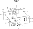
- FIG. 7 is an exploded perspective view illustrating a positional relation between a substrate and an optical box according to a comparative example.
- FIG. 8 is a perspective view illustrating a configuration of an optical scanning apparatus according to a second embodiment.
- FIG. 9 is a partial detail view illustrating the configuration of the optical scanning apparatus according to the second embodiment.
- FIG. 10A is a fragmentary cross-sectional view illustrating a configuration around a beam detect (BD) sensor as a detection unit according to the second embodiment
- FIG. 10B is a fragmentary cross-sectional view illustrating a configuration around a BD sensor according to the comparative example.
- BD beam detect
- FIG. 11A illustrates a waveform of a horizontal synchronization signal and a pulse signal according to the second embodiment
- FIG. 11B illustrates a waveform of a horizontal synchronization signal and a pulse signal according to the comparative example.
- FIGS. 1 to 7 A configuration of an image forming apparatus having an optical scanning apparatus according to a first embodiment will be described below with reference to FIGS. 1 to 7 .
- FIG. 1 is a cross-sectional view schematically illustrating the image forming apparatus D 1 .
- the image forming apparatus D 1 including an optical scanning apparatus S 1 that scans the scanned surface of a scanned member such as a photosensitive drum performs image formation on a recording medium P such as a recording sheet based on a scanned image.
- the image forming apparatus D 1 emits laser light based on image information from the optical scanning apparatus S 1 to irradiates the surface of a photosensitive drum 103 as a scanned member built in a process cartridge 102 .
- a latent image is formed on the photosensitive drum 103 .
- the latent image formed on the photosensitive drum 103 is visualized into a toner image with toner.
- the photosensitive drum 103 also serves as an image bearing member.
- the process cartridge 102 according to the present embodiment integrally includes the photosensitive drum 103 , a charging device, and a development device.
- the charging device and the development device serve as process units for acting on the photosensitive drum 103 .
- the cartridge is not limited to the process cartridge configuration.
- cartridge configurations include a developer container (such as a toner cartridge) for storing developer and a development device (such as a development cartridge) having at least a developer bearing member.
- the recording media P stored in a sheet paper cassette 104 are separated and fed one by one by a feed roller 105 and then conveyed toward the downstream side by a conveyance roller 106 .
- the toner image formed on the photosensitive drum 103 is transferred onto the recording medium P by a transfer roller 109 . More specifically, an image is formed on the recording medium P by using a toner image on the photosensitive drum 103 as a scanned member.
- the recording medium P with the toner image formed thereon is further conveyed toward the downstream side, and then heated by a fixing device 110 including a heater. Then, the toner image is thermally fixed onto the recording medium P.
- the recording medium P is discharged out of the image forming apparatus D 1 by a discharge roller 111 .
- the image forming apparatus D 1 is a monochrome image forming apparatus, the image forming apparatus D 1 may also be a full color laser beam printer.
- FIG. 2 is a perspective view illustrating the configuration of the optical scanning apparatus S 1 .
- a semiconductor laser unit 1 serves as a light source for emitting laser light L.
- An anamorphic collimator lens 2 has a function of a collimator lens and a function of a cylindrical lens.
- An aperture 3 serves as an optical diaphragm for changing the cross-sectional shape of the laser light L to a predetermined shape.
- a rotating polygon mirror 4 reflects the laser light L.
- a deflector 5 includes a circuit for driving the rotation of the rotating polygon mirror 4 . According to the present specification, the configuration of the deflector 5 includes the rotating polygon mirror 4 .
- a beam detect (BD) sensor 6 serves as a detection unit for detecting the irradiation position on the scanned surface by using the laser light L reflected by the rotating polygon mirror 4 .
- a substrate 7 is electrically connected with a semiconductor laser unit 1 .
- An f ⁇ lens 8 focuses the laser light L reflected by the rotating polygon mirror 4 on the photosensitive drum 103 at a constant speed.
- An optical box 9 stores the semiconductor laser unit 1 , the anamorphic collimator lens 2 , the aperture 3 , the deflector 5 for driving the rotation of the rotating polygon mirror 4 , and the f ⁇ lens 8 .
- An opening 9 c provided at the top of the optical box 9 is covered by a lid.
- the semiconductor laser unit 1 emits the laser light L based on an image signal received by the substrate 7 .
- the anamorphic collimator lens 2 changes the laser light L to parallel light in the main scanning cross section and changes the laser light L to converged light in the sub scanning cross section.
- Parallel light contains weak converged light and weak divergent light.
- the cross section is shaped into a predetermined shape and then focused on each reflection surface of the rotating polygon mirror 4 in a focal line shape extending in the main scanning direction.
- the rotating polygon mirror 4 is rotated at a constant angular velocity, the laser light L is deflected for scanning.
- the laser light L deflected for scanning by the rotating polygon mirror 4 enters the light receiving surface of the BD sensor 6 mounted on the substrate 7 .
- the BD sensor 6 detects the position fir starting image writing by the laser light L on the surface of a photosensitive drum in the main scanning direction and outputs a BD signal based on the timing of detection. More specifically, the BD sensor 6 detects a laser signal for controlling the irradiation position of the laser light L on the scanned surface of the scanned member and outputs a BD signal based on the timing of detection.
- the BD signal is output for each surface of the rotating polygon mirror 4 and serves as a trigger signal of control for arranging the position for starting image writing on the scanned surface in the main scanning direction.
- the f ⁇ lens 8 is an image focusing optical element.
- the f ⁇ lens 8 focuses the laser light L on the photosensitive drum 103 at a constant speed to form an image in a predetermined spot-like shape.
- Main scanning is performed when the laser light L is deflected for scanning by the rotation of the rotating polygon mirror 4 , and the laser light L scans the photosensitive drum 103 in the direction of an arrow A.
- Sub scanning is performed when the photosensitive drum 103 is driven to rotate around the axis line of the cylinder. In this way, an electrostatic latent image based on image information is formed on the surface of the photosensitive drum 103 .
- FIG. 3A is a front view illustrating the substrate 7 according to the present embodiment
- FIG. 3B is a cross-sectional view illustrating the configuration of the substrate 7 , taken along the B-B line illustrated in FIG. 3A
- the BD sensor 6 is the above-described detection unit.
- a driver integrated circuit (IC) 10 is a control unit for controlling the drive of the semiconductor laser unit 1 as a light source.
- a signal transmission connector 11 electrically connects the substrate 7 with a circuit on the side of the apparatus main body other than the substrate 7 .
- Terminals of the semiconductor laser unit 1 are inserted into through-holes 12 a to 12 d .
- the terminals of the semiconductor laser unit 1 enter the through-holes 12 a to 12 d to make electrical connection with the circuit on the substrate 7 .
- a through-hole 13 captures the laser light L to the BD sensor 6 .
- a detent notch 14 positions the substrate 7 with respect to the optical box 9 .
- a fixing portion 15 fixes the substrate 7 to the optical box 9 with a screw.
- a projection 6 a as the package of the BD sensor 6 as a detection unit is fit into the through-hole 13 in the main scanning direction.
- the BD sensor 6 is positioned while being regulated in horizontal movement. More specifically, the configuration positions the BD sensor 6 in the main scanning direction with respect to the substrate 7 corresponding to the main scanning direction on the scanned surface.
- the BD sensor 6 is fixedly attached to the substrate 7 to make electrical connection through reflow soldering.
- Reflow soldering refers to soldering by heating and melting solder pre-applied at normal temperature.
- Fitting the projection 6 a into the through-hole 13 allows accurately positioning the BD sensor 6 with respect to the through-hole 13 in the main scanning direction.
- the laser light detection surface on the side of the projection 6 a can receive the laser light L incident to the through-hole 13 .
- the signal transmission connector 11 , the BD sensor 6 , the semiconductor laser unit 1 , and the driver IC 10 are disposed in this order.
- the semiconductor laser unit 1 and the BD sensor 6 which are demanded for predetermined or highly positional accuracy are disposed near a positioning member, the semiconductor laser unit 1 and the BD sensor 6 are disposed at the center along the line connecting the semiconductor laser unit 1 and the BD sensor 6 . As also illustrated in FIG. 3B , the semiconductor laser unit 1 and the driver IC 10 are disposed on different substrate surfaces so as to sandwich the substrate 7 . The terminals of the BD sensor 6 to be electrically connected with the circuit are also disposed on the substrate surface on the side where the driver IC 10 is disposed.
- FIG. 4 is an exploded perspective view illustrating configurations of the substrate 7 and the optical box 9 according to the present embodiment.
- FIG. 5 is a cross-sectional view illustrating configurations of the substrate 7 , the optical box 9 , and the BD sensor 6 according to the present embodiment, taken along the C-C line on the optical scanning apparatus S 1 illustrated in FIG. 2 .
- FIG. 6 is a partial detail view illustrating the configuration illustrated in FIG. 5 .
- a through-hole 16 is provided in a side wall 9 a of the optical box 9 in order to capture the laser light L to the BD sensor 6 .
- the through-hole 16 is an opening, the through-hole 16 is not limited thereto and may be any structure for transmitting light.
- the through-hole 16 may be a structure filled with a transparent material for transmitting light. Therefore, in the present specification, the through-hole 16 is one of passing portions.
- First positioning members 17 are positioning projections for positioning the substrate 7 .
- the first positioning members 17 are projections protruded from the optical box 9 to the outside. These projections include portions around the opening and portions protruded from the optical box 9 toward the side of the substrate 7 to be attached thereto. These projections may have a wall surface continuously formed from the inner wall of the opening. More specifically, the projections may be shaped in such a way that the edge of the opening is thickly formed.
- a second positioning member 18 serves as a detent boss for positioning the substrate 7 .
- a screw 19 serves as a fixing member.
- the positioning projections 17 of the optical box 9 are fit into the through-hole 13 of the substrate 7 while in contact with the inner wall of the through-hole 13 . Then, the substrate 7 is positioned and attached to the optical box 9 . The positioning projections 17 protruded from the optical box 9 toward the side of the substrate 7 are engaged with the substrate 7 while in contact with the wall of the through-hole 13 of the substrate 7 . When the substrate 7 is attached to the optical box 9 , the leading edges of the positioning projections 17 is positioned within the through-hole 13 of the substrate 7 .
- the positioning projections 17 as protruded portions are shorter than the diameter of the through-hole when viewed from a direction (described below).
- FIG. 4 illustrates a state where the BD sensor 6 is separated from the substrate 7 for the sake of description.
- terminals 1 a to 1 d of the semiconductor laser unit 1 are inserted into the through-hole 12 a to 12 d , respectively, disposed on the substrate 7 .
- the semiconductor laser unit 1 is connected to the substrate 7 at four positions through soldering to make electrical conduction with the circuit.
- the substrate 7 is fixed when the fixing screw 19 is screwed into a fixing seat surface 9 b of the optical box 9 through the fixing portion 15 .
- FIG. 5 is a cross-sectional view illustrating the optical scanning apparatus S 1 after the substrate 7 is fixed to the optical box 9 .
- the laser light L emitted from the semiconductor laser unit 1 is used for scanning in the direction of the arrow A (main scanning) by the rotating polygon mirror 4 and enters the BD sensor 6 .
- the laser light L emitted from the semiconductor laser unit 1 perpendicularly intersects with the attachment surface of the substrate 7 to which the terminals of the semiconductor laser unit 1 are attached.
- the laser light L reflected by the rotating polygon mirror 4 advances straight toward the BD sensor 6 , the laser light L does not perpendicularly intersect with the attachment surface but obliquely intersects with the attachment surface.
- a configuration of the vicinity of the BD sensor 6 will be described in detail below with reference to FIG. 6 .
- the laser light L reflected by the rotating polygon mirror 4 passes through the through-hole 16 of the optical box 9 and the through-hole 13 of the substrate 7 , and enters the BD sensor 6 .
- the positioning projections 17 provided on the optical box 9 come in contact with and fit into the inner wall of the through-hole 13 provided in the substrate 7 .
- the substrate 7 is positioned in the main scanning direction of the optical box 9 and substrate 7 corresponding to the main scanning direction on the scanned surface. Since the positioning projections 17 provided on the optical box 9 and the BD sensor 6 are fit into the through-hole 13 and positioned, the BD sensor 6 can be positioned to the optical box 9 with high accuracy.
- FIG. 7 is an exploded perspective view illustrating a positioning method used when positioning the substrate 7 to the optical box 9 according to a comparative example. Instead of fitting by the through-hole 13 , this method uses fitting by a boss and a through-hole generally used for positioning of a machine part.
- FIG. 7 illustrates a positioning boss 21 and a positioning hole 22 .
- the positioning boss 21 is fit into the positioning hole 22
- the detent boss 18 is fit into the detent notch 14
- the substrate 71 is positioned to the optical box 9 .
- a distance d from the positioning boss 21 to the through-hole 13 of the substrate 71 varies in the manufacturing process. If the through-hole 13 deviates to a position 13 ′ drawn with dashed lines, for example, the BD sensor 6 will be fit into the through-hole drawn with dashed lines and accordingly fixed to the optical box 9 being deviated from a predetermined or desired position.
- a video signal is output in synchronization with the timing for starting image writing which comes when a fixed time period has elapsed since the BD signal was output from the BD sensor 6 . Therefore, if the BD sensor 6 deviates from the predetermined or desired position, the position for starting image writing will also deviate. This shifts the irradiation position on the scanned surface of the photosensitive drum 103 . Thus, horizontal margins in the image printed on the recording medium P become larger or smaller than the ideal width. According to the present embodiment, as illustrated in FIG.
- the optical box 9 and the BD sensor 6 are positioned to the through-hole 13 at the deviated position, making it possible to restrain the deviation of the position for starting image writing.
- the expression of the positional deviation is exaggerated.
- FIG. 8 is an exploded perspective view illustrating configurations of the substrate 7 and an optical box 29 according to the second embodiment.
- FIG. 9 is a fragmentary cross-sectional view illustrating configurations of the substrate 7 , the optical box 29 , and the BD sensor 6 according to the second embodiment.
- the present embodiment illustrated in FIG. 8 differs from the first embodiment illustrated in FIG. 4 in that a notch 36 provided in a side wall 29 a of the optical box 29 serves as a passing portion for capturing the laser light L to the BD sensor 6 .
- the through-hole 16 serves as a passing portion in FIG. 4
- the notch 36 is used in the present embodiment in consideration of the formability of the optical box 29 made of resin.
- the present embodiment illustrated in FIG. 9 differs from the first embodiment illustrated in FIG. 6 in that the optical path for capturing the laser light L to the BD sensor 6 has a cross-sectional shape.
- the cross-sectional shape of a side wall 37 a of the positioning projections 37 as protruded portions on the optical path side is parallel to the angle of the incident light L to the BD sensor 6 .
- the side wall 37 a is provided in parallel with the straight traveling direction in which the laser light L advances straight to the BD sensor 6 .
- the positioning projections 37 as protruded portions are formed around the notch 36 .
- an inner wall 36 a of the notch 36 is also formed in parallel with the angle of the incident light L to the BD sensor 6 .
- the side wall 37 a of the positioning projections 37 and the inner wall 36 a of the notch 36 form a continuous wall and are parallel to the angle of the incident light to the BD sensor 6 .
- the side wall 37 a of the positioning projections 37 and the inner wall 36 a of the notch 36 are parallel to the laser light L, and therefore do not perpendicularly intersect with the line connecting the light source and the detection unit but obliquely intersects with the line.
- the inner wall 36 a is referred to as a first inner wall 36 a
- the inner wall facing the first inner wall 36 a is referred to as a second inner wall 36 b
- the second inner wall 36 b may also include a wall or surface parallel to the laser light L.
- the second inner walls 36 b is partially formed of a surface parallel to the laser light L and partially formed of a surface intersecting with the line.
- the notch 36 is formed to avoid an undercut-shaped optical path and a complicated mold structure.
- FIG. 10A is a fragmentary cross-sectional view illustrating the periphery of the BD sensor 6 according to the present embodiment.
- FIG. 10B is a fragmentary cross-sectional view illustrating the periphery of the BD sensor 6 according to the comparative example of the first embodiment illustrated in FIG. 7 .
- FIG. 11A illustrates a waveform of the BD signal of the BD sensor 6 illustrated in FIG. 10A
- FIG. 11B illustrates a waveform of the BD signal of the BD sensor 6 illustrated in FIG. 10B .
- the laser light L to be captured to a light reception portion 6 a of the BD sensor 6 is used for scanning by the rotating polygon mirror 4 . Reflection conditions of the laser light L until the laser light L is captured to the light reception portion 6 a are illustrated in FIGS. 10A and 10B .
- laser light L 1 is light at the timing of incidence to the light reception portion 6 a
- laser light L 2 is light at the timing after a fixed time period has elapsed since the timing of incidence of the laser light L 1 .
- the laser light L 2 leads the laser light L 1 by a light angle of ⁇ 1 .
- the side walls 36 a and 37 a are side walls on the downstream side of the BD optical path of the optical box 29 in the rotational direction.
- laser light L 11 is light at the timing of incidence to the light reception portion 6 a
- laser light L 22 is light at the timing after a fixed time period has elapsed since the timing of incidence of the laser light L 11 .
- the laser light L 22 leads the laser light L 11 by a light angle of ⁇ 2 .
- the configuration illustrated in FIG. 10A differs from the configuration illustrated in FIG. 10B in the state of the inner wall 7 a . More specifically, the inner wall 7 a of the through-hole 13 of the substrate 7 illustrated in FIG.
- the optical box 29 is covered by the positioning projections 37 of the optical box 29 while the inner wall 7 a illustrated in FIG. 10B is exposed to the laser light L. Since the through-hole 13 and outer shape of the substrate 7 are normally formed by pressing, the inner wall 7 a and edge surfaces are perpendicular to a substrate surface 7 c of the substrate 7 .
- the optical box 29 is manufactured by injection molding of resin, the optical box 29 is highly flexible in angles and shapes as with the side walls 36 a or 37 a .
- an optical box is made of black resin with additive fillers such as a glass fiber to improve the strength, and therefore provides non-glossy surfaces hardly having reflectiveness. Therefore, although the quantity of re-incidence light is small even in the form according to the first embodiment, geometric measures may be taken for re-incidence of reflected light regardless of the surface reflectance, like the second embodiment.
- the top graph in FIG. 11A illustrates a waveform 40 of the light quantity E assigned to the vertical axis.
- the waveform 40 starts rising.
- the laser light L reaches the center of the light reception portion 6 a , i.e., at a timing when the light flux enters the light reception portion 6 a to the maximum extent, the light quantity E is maximized.
- the bottom graphs in FIGS. 11A and 11B illustrate a signal level V assigned to the vertical axis. Referring to the top graphs in FIGS.
- the circuit is configured to change the signal level V when the waveforms 40 and 42 pass through a set threshold value 41 .
- the laser light L 2 which leads the laser light L 1 entering the light reception portion 6 a by a light angle of ⁇ 1 is approximately parallel to the side wall 37 a . Therefore, the laser light L 2 is reflected by neither the side wall 37 a of the projections 37 nor the inner wall 7 a of the through-hole 13 of the substrate 7 . Therefore, the BD signal output from the BD sensor 6 has the waveform 40 as illustrated in FIG. 11A .
- FIG. 10A the laser light L 2 which leads the laser light L 1 entering the light reception portion 6 a by a light angle of ⁇ 1 is approximately parallel to the side wall 37 a . Therefore, the laser light L 2 is reflected by neither the side wall 37 a of the projections 37 nor the inner wall 7 a of the through-hole 13 of the substrate 7 . Therefore, the BD signal output from the BD sensor 6 has the waveform 40 as illustrated in FIG. 11A
- the waveform 42 provides two different mountains, as illustrated in the top graph in FIG. 11B , and accordingly a pulse signal is also output twice as illustrated in the bottom graph in FIG. 11B since a pulse signal is output when the waveform 42 exceeds the threshold value 41 .
- an image controller may incorrectly detect the timing for starting image writing, possibly affecting the position for starting image writing. More specifically, there may be a deviation of the irradiation position of the surface as a scanned surface of the photosensitive drum 103 as a scanned member. Therefore, it is necessary to avoid light re-incidence to the light reception portion 6 a of the BD sensor 6 .
- the present embodiment allows restraining a deviation of the position of the BD sensor 6 for generating the BD signal to prevent a deviation of the generation timing of the BD signal for controlling the position for starting image writing.
- the present embodiment further allows forming the side wall 36 a as the optical path for light incidence to the BD sensor 6 of the optical box 29 in suitable angle and shape to prevent light incidence to the inner wall 7 a of the substrate 7 . This makes it possible to restrain light re-incidence to the light reception portion 6 a of the BD sensor 6 to prevent a deviation of the output timing due to incorrect detection of the BD signal to a further extent, thus achieving image formation with a stable position for starting image writing.
- the present disclosure makes it possible to attach a detection unit to an optical box with sufficient accuracy.
Landscapes
- Physics & Mathematics (AREA)
- General Physics & Mathematics (AREA)
- Optics & Photonics (AREA)
- Laser Beam Printer (AREA)
- Mechanical Optical Scanning Systems (AREA)
- Facsimile Scanning Arrangements (AREA)
Abstract
Description
Claims (11)
Applications Claiming Priority (2)
| Application Number | Priority Date | Filing Date | Title |
|---|---|---|---|
| JP2018083812A JP2019191356A (en) | 2018-04-25 | 2018-04-25 | Optical scanner and image formation device |
| JP2018-083812 | 2018-04-25 |
Publications (2)
| Publication Number | Publication Date |
|---|---|
| US20190332029A1 US20190332029A1 (en) | 2019-10-31 |
| US10838318B2 true US10838318B2 (en) | 2020-11-17 |
Family
ID=68290713
Family Applications (1)
| Application Number | Title | Priority Date | Filing Date |
|---|---|---|---|
| US16/373,499 Expired - Fee Related US10838318B2 (en) | 2018-04-25 | 2019-04-02 | Optical scanning apparatus and image forming apparatus |
Country Status (2)
| Country | Link |
|---|---|
| US (1) | US10838318B2 (en) |
| JP (1) | JP2019191356A (en) |
Families Citing this family (2)
| Publication number | Priority date | Publication date | Assignee | Title |
|---|---|---|---|---|
| EP4261620B1 (en) * | 2022-04-15 | 2025-07-30 | Ricoh Company, Ltd. | Developing device, process cartridge, and image forming apparatus |
| JP2024021978A (en) * | 2022-08-05 | 2024-02-16 | キヤノン株式会社 | Optical scanning device and image forming device |
Citations (14)
| Publication number | Priority date | Publication date | Assignee | Title |
|---|---|---|---|---|
| US20030173508A1 (en) * | 2002-02-28 | 2003-09-18 | Canon Kabushiki Kaisha | Light source unit and scanning optical apparatus using the same |
| US20060045149A1 (en) * | 2004-08-27 | 2006-03-02 | Pentax Corporation | Laser scanning device |
| US20060098994A1 (en) * | 2003-08-13 | 2006-05-11 | Brother Kogyo Kabushiki Kaisha | Optical scanning device |
| US20070146738A1 (en) * | 2005-12-22 | 2007-06-28 | Tomohiro Nakajima | Multiple-beam scanning device and image forming apparatus having the multiple-beam scanning device |
| US20090052944A1 (en) * | 2007-08-20 | 2009-02-26 | Nobuaki Kubo | Light source unit, optical scan apparatus, and image formation apparatus |
| US20090060583A1 (en) * | 2007-08-31 | 2009-03-05 | Taku Amada | Light source unit, optical scan apparatus, and image formation apparatus |
| US20100060963A1 (en) * | 2008-09-05 | 2010-03-11 | Shinsuke Miyake | Optical scanning device and image forming apparatus |
| US20100183337A1 (en) * | 2009-01-16 | 2010-07-22 | Nobuaki Kubo | Light source apparatus, optical-beam scanning apparatus, and image forming apparatus |
| US20130033557A1 (en) * | 2011-08-03 | 2013-02-07 | Samsung Electronics Co., Ltd | Light scanning unit and image forming apparatus employing the same |
| US20130222513A1 (en) * | 2012-02-23 | 2013-08-29 | Kyocera Document Solutions Inc. | Optical scanning device and image forming apparatus including the same |
| US20150268581A1 (en) * | 2014-03-19 | 2015-09-24 | Canon Kabushiki Kaisha | Image forming apparatus and correction data generation method |
| US20160238965A1 (en) * | 2015-02-17 | 2016-08-18 | Canon Kabushiki Kaisha | Optical scanning device |
| JP2016151666A (en) | 2015-02-17 | 2016-08-22 | キヤノン株式会社 | Scanning optical device |
| US20170123339A1 (en) * | 2014-06-20 | 2017-05-04 | Kyocera Document Solutions Inc. | Optical scanning device and image forming apparatus including the same |
-
2018
- 2018-04-25 JP JP2018083812A patent/JP2019191356A/en active Pending
-
2019
- 2019-04-02 US US16/373,499 patent/US10838318B2/en not_active Expired - Fee Related
Patent Citations (14)
| Publication number | Priority date | Publication date | Assignee | Title |
|---|---|---|---|---|
| US20030173508A1 (en) * | 2002-02-28 | 2003-09-18 | Canon Kabushiki Kaisha | Light source unit and scanning optical apparatus using the same |
| US20060098994A1 (en) * | 2003-08-13 | 2006-05-11 | Brother Kogyo Kabushiki Kaisha | Optical scanning device |
| US20060045149A1 (en) * | 2004-08-27 | 2006-03-02 | Pentax Corporation | Laser scanning device |
| US20070146738A1 (en) * | 2005-12-22 | 2007-06-28 | Tomohiro Nakajima | Multiple-beam scanning device and image forming apparatus having the multiple-beam scanning device |
| US20090052944A1 (en) * | 2007-08-20 | 2009-02-26 | Nobuaki Kubo | Light source unit, optical scan apparatus, and image formation apparatus |
| US20090060583A1 (en) * | 2007-08-31 | 2009-03-05 | Taku Amada | Light source unit, optical scan apparatus, and image formation apparatus |
| US20100060963A1 (en) * | 2008-09-05 | 2010-03-11 | Shinsuke Miyake | Optical scanning device and image forming apparatus |
| US20100183337A1 (en) * | 2009-01-16 | 2010-07-22 | Nobuaki Kubo | Light source apparatus, optical-beam scanning apparatus, and image forming apparatus |
| US20130033557A1 (en) * | 2011-08-03 | 2013-02-07 | Samsung Electronics Co., Ltd | Light scanning unit and image forming apparatus employing the same |
| US20130222513A1 (en) * | 2012-02-23 | 2013-08-29 | Kyocera Document Solutions Inc. | Optical scanning device and image forming apparatus including the same |
| US20150268581A1 (en) * | 2014-03-19 | 2015-09-24 | Canon Kabushiki Kaisha | Image forming apparatus and correction data generation method |
| US20170123339A1 (en) * | 2014-06-20 | 2017-05-04 | Kyocera Document Solutions Inc. | Optical scanning device and image forming apparatus including the same |
| US20160238965A1 (en) * | 2015-02-17 | 2016-08-18 | Canon Kabushiki Kaisha | Optical scanning device |
| JP2016151666A (en) | 2015-02-17 | 2016-08-22 | キヤノン株式会社 | Scanning optical device |
Also Published As
| Publication number | Publication date |
|---|---|
| US20190332029A1 (en) | 2019-10-31 |
| JP2019191356A (en) | 2019-10-31 |
Similar Documents
| Publication | Publication Date | Title |
|---|---|---|
| US6825869B2 (en) | Apparatus to generate laser beam detect signal | |
| US10389897B2 (en) | Light scanning apparatus with overlapped holders for light sources, and image forming apparatus therewith | |
| US10838318B2 (en) | Optical scanning apparatus and image forming apparatus | |
| US11194264B2 (en) | Optical scanning apparatus with offset beam detect sensor for scan line positioning in sub-scan direction and image forming apparatus with optical scanning apparatus | |
| US10698335B2 (en) | Optical scanning apparatus and image forming apparatus | |
| US8723910B2 (en) | Optical scanning device and image forming apparatus using same | |
| JP3564026B2 (en) | Optical scanning device, multi-beam optical scanning device, and image forming apparatus using the same | |
| US8570631B2 (en) | Optical scanning device and image forming apparatus | |
| CN1316283C (en) | Multi-beam laser scanning unit and laser-beam deflection compensating method | |
| US9791802B2 (en) | Scanning optical device and image forming apparatus | |
| US10649360B2 (en) | Optical scanning device | |
| JP6584087B2 (en) | Scanning optical device | |
| US8305413B2 (en) | Optical writing apparatus and image forming apparatus, configured to include synchronous detector | |
| US10338491B2 (en) | Optical scanning apparatus and optical scanning apparatus system | |
| WO2018092830A1 (en) | Optical scanning device and image forming apparatus | |
| US10042281B2 (en) | Image forming apparatus | |
| US6888559B2 (en) | Laser beam scanner forming a scanning line along a main scanning direction | |
| JP6436657B2 (en) | Optical scanning apparatus and image forming apparatus | |
| JP7395386B2 (en) | Scanner unit and image forming device using it | |
| JP2019174816A (en) | Scanning optical device | |
| JP2005292845A (en) | Scanning optical system, multi-beam scanning optical system, and image forming apparatus using the same | |
| US20210212217A1 (en) | Method of mounting electronic component, substrate and an optical scanning apparatus | |
| JP2008058884A (en) | Scanning exposure apparatus and image forming apparatus having the same | |
| JP2011129812A (en) | Light source device, and exposure device | |
| JP2004219770A (en) | Optical scanning device and image forming apparatus |
Legal Events
| Date | Code | Title | Description |
|---|---|---|---|
| FEPP | Fee payment procedure |
Free format text: ENTITY STATUS SET TO UNDISCOUNTED (ORIGINAL EVENT CODE: BIG.); ENTITY STATUS OF PATENT OWNER: LARGE ENTITY |
|
| AS | Assignment |
Owner name: CANON KABUSHIKI KAISHA, JAPAN Free format text: ASSIGNMENT OF ASSIGNORS INTEREST;ASSIGNOR:FUKUHARA, HIROYUKI;REEL/FRAME:049602/0020 Effective date: 20190318 |
|
| STPP | Information on status: patent application and granting procedure in general |
Free format text: NON FINAL ACTION MAILED |
|
| STPP | Information on status: patent application and granting procedure in general |
Free format text: FINAL REJECTION MAILED |
|
| STPP | Information on status: patent application and granting procedure in general |
Free format text: NOTICE OF ALLOWANCE MAILED -- APPLICATION RECEIVED IN OFFICE OF PUBLICATIONS |
|
| STPP | Information on status: patent application and granting procedure in general |
Free format text: PUBLICATIONS -- ISSUE FEE PAYMENT VERIFIED |
|
| STCF | Information on status: patent grant |
Free format text: PATENTED CASE |
|
| LAPS | Lapse for failure to pay maintenance fees |
Free format text: PATENT EXPIRED FOR FAILURE TO PAY MAINTENANCE FEES (ORIGINAL EVENT CODE: EXP.); ENTITY STATUS OF PATENT OWNER: LARGE ENTITY |
|
| STCH | Information on status: patent discontinuation |
Free format text: PATENT EXPIRED DUE TO NONPAYMENT OF MAINTENANCE FEES UNDER 37 CFR 1.362 |
|
| FP | Lapsed due to failure to pay maintenance fee |
Effective date: 20241117 |