US10838288B2 - Projection apparatus and imaging module thereof - Google Patents
Projection apparatus and imaging module thereof Download PDFInfo
- Publication number
- US10838288B2 US10838288B2 US16/402,177 US201916402177A US10838288B2 US 10838288 B2 US10838288 B2 US 10838288B2 US 201916402177 A US201916402177 A US 201916402177A US 10838288 B2 US10838288 B2 US 10838288B2
- Authority
- US
- United States
- Prior art keywords
- optical element
- actuator
- carrier
- active display
- display surface
- Prior art date
- Legal status (The legal status is an assumption and is not a legal conclusion. Google has not performed a legal analysis and makes no representation as to the accuracy of the status listed.)
- Active
Links
Images


Classifications
-
- G—PHYSICS
- G02—OPTICS
- G02B—OPTICAL ELEMENTS, SYSTEMS OR APPARATUS
- G02B26/00—Optical devices or arrangements for the control of light using movable or deformable optical elements
- G02B26/08—Optical devices or arrangements for the control of light using movable or deformable optical elements for controlling the direction of light
- G02B26/0816—Optical devices or arrangements for the control of light using movable or deformable optical elements for controlling the direction of light by means of one or more reflecting elements
-
- G—PHYSICS
- G03—PHOTOGRAPHY; CINEMATOGRAPHY; ANALOGOUS TECHNIQUES USING WAVES OTHER THAN OPTICAL WAVES; ELECTROGRAPHY; HOLOGRAPHY
- G03B—APPARATUS OR ARRANGEMENTS FOR TAKING PHOTOGRAPHS OR FOR PROJECTING OR VIEWING THEM; APPARATUS OR ARRANGEMENTS EMPLOYING ANALOGOUS TECHNIQUES USING WAVES OTHER THAN OPTICAL WAVES; ACCESSORIES THEREFOR
- G03B21/00—Projectors or projection-type viewers; Accessories therefor
- G03B21/14—Details
- G03B21/20—Lamp housings
- G03B21/2006—Lamp housings characterised by the light source
-
- G—PHYSICS
- G02—OPTICS
- G02B—OPTICAL ELEMENTS, SYSTEMS OR APPARATUS
- G02B26/00—Optical devices or arrangements for the control of light using movable or deformable optical elements
- G02B26/08—Optical devices or arrangements for the control of light using movable or deformable optical elements for controlling the direction of light
- G02B26/0875—Optical devices or arrangements for the control of light using movable or deformable optical elements for controlling the direction of light by means of one or more refracting elements
-
- G—PHYSICS
- G02—OPTICS
- G02B—OPTICAL ELEMENTS, SYSTEMS OR APPARATUS
- G02B27/00—Optical systems or apparatus not provided for by any of the groups G02B1/00 - G02B26/00, G02B30/00
- G02B27/09—Beam shaping, e.g. changing the cross-sectional area, not otherwise provided for
- G02B27/0938—Using specific optical elements
- G02B27/095—Refractive optical elements
- G02B27/0955—Lenses
-
- G—PHYSICS
- G02—OPTICS
- G02B—OPTICAL ELEMENTS, SYSTEMS OR APPARATUS
- G02B27/00—Optical systems or apparatus not provided for by any of the groups G02B1/00 - G02B26/00, G02B30/00
- G02B27/09—Beam shaping, e.g. changing the cross-sectional area, not otherwise provided for
- G02B27/0938—Using specific optical elements
- G02B27/0977—Reflective elements
-
- G—PHYSICS
- G03—PHOTOGRAPHY; CINEMATOGRAPHY; ANALOGOUS TECHNIQUES USING WAVES OTHER THAN OPTICAL WAVES; ELECTROGRAPHY; HOLOGRAPHY
- G03B—APPARATUS OR ARRANGEMENTS FOR TAKING PHOTOGRAPHS OR FOR PROJECTING OR VIEWING THEM; APPARATUS OR ARRANGEMENTS EMPLOYING ANALOGOUS TECHNIQUES USING WAVES OTHER THAN OPTICAL WAVES; ACCESSORIES THEREFOR
- G03B21/00—Projectors or projection-type viewers; Accessories therefor
- G03B21/005—Projectors using an electronic spatial light modulator but not peculiar thereto
-
- G—PHYSICS
- G03—PHOTOGRAPHY; CINEMATOGRAPHY; ANALOGOUS TECHNIQUES USING WAVES OTHER THAN OPTICAL WAVES; ELECTROGRAPHY; HOLOGRAPHY
- G03B—APPARATUS OR ARRANGEMENTS FOR TAKING PHOTOGRAPHS OR FOR PROJECTING OR VIEWING THEM; APPARATUS OR ARRANGEMENTS EMPLOYING ANALOGOUS TECHNIQUES USING WAVES OTHER THAN OPTICAL WAVES; ACCESSORIES THEREFOR
- G03B21/00—Projectors or projection-type viewers; Accessories therefor
- G03B21/14—Details
- G03B21/142—Adjusting of projection optics
-
- H—ELECTRICITY
- H04—ELECTRIC COMMUNICATION TECHNIQUE
- H04N—PICTORIAL COMMUNICATION, e.g. TELEVISION
- H04N9/00—Details of colour television systems
- H04N9/12—Picture reproducers
- H04N9/31—Projection devices for colour picture display, e.g. using electronic spatial light modulators [ESLM]
- H04N9/3141—Constructional details thereof
-
- G—PHYSICS
- G03—PHOTOGRAPHY; CINEMATOGRAPHY; ANALOGOUS TECHNIQUES USING WAVES OTHER THAN OPTICAL WAVES; ELECTROGRAPHY; HOLOGRAPHY
- G03B—APPARATUS OR ARRANGEMENTS FOR TAKING PHOTOGRAPHS OR FOR PROJECTING OR VIEWING THEM; APPARATUS OR ARRANGEMENTS EMPLOYING ANALOGOUS TECHNIQUES USING WAVES OTHER THAN OPTICAL WAVES; ACCESSORIES THEREFOR
- G03B2205/00—Adjustment of optical system relative to image or object surface other than for focusing
- G03B2205/0053—Driving means for the movement of one or more optical element
Definitions
- the invention relates to a projection apparatus and an imaging module thereof, and more particularly to a projection apparatus and an imaging module having an image displacement device.
- a projection apparatus is a device that can project an image onto a projection screen for presentation to a user.
- the image presented on the projection screen can have a finer image quality when the resolution of the image projected by the projection apparatus is increased.
- images of 4K (3840 ⁇ 2160 pixels) or more have become more popular in recent years. Therefore, the manufacturers work hard for improving the resolution of the projection apparatus.
- a larger high-resolution imaging element such as LCD, DMD, LCoS, etc.
- an additional component is employed.
- these practices may increase the size of the projection apparatus, and the associated optical or mechanical components must also become larger, resulting in increased cost and volume. Therefore, how to reduce the volume of the projection apparatus at the same time when improving the resolution of the projection apparatus is a focus of attention of those skilled in the art.
- the invention provides an imaging module, which provides an arrangement effectively reducing the distance between the display element and the optical element of the image displacement device, thereby reducing the cost and downsizing the projection apparatus using the imaging module.
- the invention further provides a projection apparatus having a more compacted size.
- an embodiment of the invention provides an imaging module, which includes a display element and an image displacement device.
- the display element includes an active display surface, and the active display surface is adapted to receive an illumination beam and convert the illumination beam into an image beam, and the image beam is transmitted by the active display surface.
- the image displacement device includes an optical element, a carrier, a base, and at least one actuator.
- the optical element is disposed on the carrier.
- the optical element is located on a transmission path of the image beam and is adapted to allow the image beam to pass therethrough.
- the at least one actuator is disposed on the base.
- One end of the at least one actuator is connected to the carrier to drive the optical element on the carrier to swing relative to the base.
- a plane where the active display surface is located is a reference plane.
- An orthographic projection area of the at least one actuator on the reference plane does not overlap with an orthographic projection area of the active display surface.
- an embodiment of the invention provides a projection apparatus, which includes an illumination system, a projection lens and an imaging module.
- the illumination system is adapted to provide an illumination beam.
- the imaging module includes a display element and an image displacement device.
- the display element includes an active display surface, and the active display surface is adapted to receive an illumination beam and convert the illumination beam into an image beam, and the image beam is transmitted by the active display surface.
- the image displacement device includes an optical element, a carrier, a base, and at least one actuator.
- the optical element is disposed on the carrier.
- the optical element is located on a transmission path of the image beam and is adapted to allow the image beam to pass therethrough.
- the image beam passes through the optical element and is transmitted to the projection lens.
- the at least one actuator is disposed on the base. One end of the at least one actuator is connected to the carrier to drive the optical element on the carrier to swing relative to the base.
- a plane on which the active display surface is located is a reference plane. An orthographic projection area of the at least one actuator on the reference plane does not overlap with an orthographic projection area of the active display surface.
- the imaging module of the embodiment of the invention can greatly reduce the distance from the display element to the optical element, and thus the rear focus distance of the projection apparatus using the imaging module can be greatly reduced. Therefore, the volume and cost of the projection apparatus can be reduced, and the optical quality of the projection apparatus can also be improved.
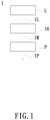
- FIG. 1 is a schematic view of a projection apparatus according to an embodiment of the invention.
- FIGS. 2A-2C are schematic views of an imaging module according to an embodiment of the invention.
- the description of “A” component facing “B” component herein may contain the situations that “A” component directly faces “B” component or one or more additional components are between “A” component and “B” component.
- the description of “A” component “adjacent to” “B” component herein may contain the situations that “A” component is directly “adjacent to” “B” component or one or more additional components are between “A” component and “B” component. Accordingly, the drawings and descriptions will be regarded as illustrative in nature and not as restrictive.
- FIG. 1 is a schematic view of a projection apparatus according to an embodiment of the invention.
- the projection apparatus 1 includes an illumination system L, an imaging module 10 and a projection lens P.
- the imaging module 10 is disposed on a transmission path of an illumination beam IL provided by the illumination system L and is adapted to convert the illumination beam IL into an image beam IM.
- the projection lens P is disposed on a transmission path of the image beam IM.
- the image beam IM is for forming a projection beam IP after passing through the projection lens P, thereby forming an image frame on a projection surface.
- FIG. 1 is exemplified by one imaging module 10 ; however, the number of imaging modules 10 may be plural in other embodiments.
- the illumination system L may include, for example, a high pressure mercury lamp, a laser diode, or a light emitting diode to generate the illumination beam IL, but the invention is not limited thereto.
- FIGS. 2A-2C are schematic views of the imaging module 10 shown in FIG. 1 .
- FIG. 2A is an exploded view of a display element and an image displacement device
- FIG. 2B is a schematic view of a front projection of the relative positions of some components of the imaging module 10
- FIG. 2C is a cross-sectional side view of the imaging module 10 .
- the imaging module 10 of the embodiment includes a display element 11 and an image displacement device 23 .
- the imaging module 10 is located on a transmission path of the image beam IM.
- the image displacement device 23 is disposed between the display element 11 and the projection lens P.
- the display element 11 includes an active display surface 111 .
- the active display surface 111 is adapted to receive the illumination beam IL, convert the illumination beam IL into the image beam IM, and reflect the image beam IM.
- the display element 11 is a transmissive display element, such as a light transmissive liquid crystal panel, and accordingly the active display surface 111 is adapted to receive the illumination beam IL, convert the illumination beam IL into the image beam IM, and transmit the image beam IM to the image displacement device 23 .
- the image displacement device 23 includes an optical element 131 , a carrier 232 , a base 236 , and actuators 233 and 234 .
- the optical element 131 is disposed on the carrier 232 .
- the optical element 131 is located on the transmission path of the image beam IM and is adapted to allow the image beam IM to pass therethrough.
- the embodiment is exemplified by two actuators, but the invention is not limited thereto. In other embodiments, the same effect may also be achieved by employing only one actuator or four actuators.
- the actuators 233 and 234 are disposed on the base 236 , wherein the base 236 is fixed in the projection apparatus 1 .
- One end of the actuator 233 and one end of the actuator 234 are respectively connected to the carrier 232 to drive the optical element 131 on the carrier 232 to swing relative to the base 236 , so that the optical element 131 changes the image characteristics of the image beam IM, specifically, changes the optical path of the image beam IM. Therefore, by the arrangement of the image displacement device 23 , the image resolution of the projection apparatus 1 or the image quality of the projected image frame can be improved, for example, but the invention is not limited thereto.
- FIG. 2B is a schematic orthographic projection view of the relative positions of some of the components of the imaging module.
- the plane where the active display surface 111 of the display element 11 is located is defined as a reference plane S.
- the orthographic projection of the active display surface 111 on the reference plane S is the area of the active display surface 111 p ;
- the orthographic projection of the optical element 131 on the reference plane S is the area of the optical element 131 p ;
- the orthographic projection of the actuator 233 on the reference plane S is the area of the actuator 233 p ;
- the orthographic projection of the actuator 234 on the reference plane S is the area of the actuator 234 p .
- a size of the area of optical element 131 p is larger than a size of the area of active display surface 111 p , so that the optical path of the all image beam IM transmitted from the active display surface 111 can be changed by the optical element 131 .
- the areas of actuators 233 p and 234 p of the orthographic projections of the actuators 233 and 234 on the reference plane S do not overlap with the area of active display surface 111 p , that is, the actuators 233 and 234 do not overlap or have mechanism interference with the active display surface 111 , wherein it is to be noted that the aforementioned so-called overlap includes partial overlap.
- the display element 11 can be as close as possible to the optical element 131 without being blocked by the actuator 233 or 234 .
- the active display surface 111 can be close to the optical element 131 , so that the volume of the imaging module 10 can be greatly reduced, and thereby reducing the cost and compacting the size of the projection apparatus 1 .
- FIG. 2C is a side view of the imaging module viewed in the direction A in FIG. 2A .
- the distance from the active display surface 111 of the display element 11 to the optical element 131 is the first distance d 1 .
- the normal line of the center of the active display surface 111 is defined as the reference line L.
- the orthographic projection of the actuator 233 or 234 on the reference line L is the line segment L 1 , and the end point of the line segment L 1 adjacent to the display element 11 and away from the optical element 131 is the reference point P 1 .
- the distance from the reference point P 1 to the optical element 131 is the second distance d 2 .
- the first distance d 1 is smaller than the second distance d 2 .
- the area of actuator 233 p and the area of active display surface 111 p have a length d 233 between them, and the area of actuator 234 p and the area of active display surface 111 p have a length d 234 between them.
- the areas of actuators 233 p and 234 p of the actuators 233 and 234 have a sufficient distant therebetween the area of active display surface 111 p of the active display surface 111 , that is, the lengths d 233 and d 234 are long enough, so that the active display surface 111 does not overlap or contact with the actuators 233 and 234 . From FIG.
- the actuators 233 and 234 have a certain distance therebetween the optical element 131 and the display element 11 , the display element 11 can be as close as possible to the optical element 131 without being blocked by or having mechanism interference with the actuator 233 or 234 . Therefore, the rear focus distance of the projection apparatus 1 (i.e., the distance from the active display surface 111 to the projection lens P) can be greatly reduced.
- the smaller rear focus distance can reduce the cost and compact the size of the projection apparatus 1 .
- a projection lens P with smaller size (a lens using a smaller effective light diameter) can be used, and the optical quality of the projection apparatus 1 can also be improved.
- the rear focus distance is the distance between the active display surface 111 and the projection lens P.
- other light transmission elements such as prism or mirror, may be disposed between the active display surface 111 and the projection lens P to transmit the image beam IM to the projection lens P.
- the lengths d 233 and d 234 shown in FIGS. 2B and 2C are only an example, and the invention is limited thereto.
- the lengths d 233 and d 234 may be any value as long as that the areas of actuator 233 p and 234 p of the orthographic projections of the actuators 233 and 234 on the reference plane S do not overlap the area of active display surface 111 p of the active display surface 111 .
- the optical element 131 includes a flat glass.
- the flat glass includes a light incident surface 1311 and a light exit surface 1313 , and the light incident surface 1311 is opposite to the light exit surface 1313 .
- the image beam IM formed by the display element 11 is incident on the optical element 131 through the light incident surface 1311 .
- the illumination beam IL is firstly incident on the optical element 131 through the light exit surface 1313 and then transmitted to the display element 11 through the light incident surface 1311 .
- the light incident surface 1311 and the light exit surface 1313 are parallel to the active display surface 111 when the actuators 233 and 234 do not drive the optical element 131 on the carrier 232 to swing relative to the base 236 .
- the light incident surface 1311 and the light exit surface 1313 are not parallel to the active display surface 111 when the actuators 233 and 234 drive the optical element 131 on the carrier 232 to swing relative to the base 236 . Therefore, the optical element 131 can change the optical path of the image beam IM by configuring the actuators 233 and 234 to drive the optical element 131 to swing relative to the base 236 .
- the image resolution of the projection apparatus 1 or the image quality of the image frame can be improved for example, but the invention is not limited thereto.
- the carrier 232 includes a first hollow region 2321 , and the optical element 131 is disposed within the first hollow region 2321 .
- the base 236 includes a second hollow region 2361 , and the carrier 232 is located within the second hollowed region 2361 .
- the structures and shapes of the carrier 232 and the base 236 shown in FIGS. 2A and 2C are merely examples, and the invention is not limited thereto.
- the light incident surface 1311 of the optical element 131 and the active display surface 111 of the display element 11 may be, for example, rectangular. As shown in FIG. 2B , in the embodiment, the area of the light incident surface 1311 is larger than the area of the active display surface 111 . Therefore, by the design of the carrier 232 , the lengths d 233 and d 234 can be long enough, so that the areas of actuators 233 p and 234 p of the actuators 233 and 234 have a sufficient distance therebetween the area of the active display surface 111 p , and accordingly the area of active display surface 111 p of the active display surface 111 does not overlap or contact with the areas of actuators 233 p and 234 p .
- the display element 11 can be as close as possible to the optical element 131 without being blocked by or having mechanism interference with the actuator 233 or 234 . Therefore, the rear focus distance of the projection apparatus 1 can be greatly reduced without increasing the cost of the optical element.
- the embodiment is exemplified by that the image displacement device 23 is disposed with two actuators 233 and 234 , but the invention does not limit the number and position of the actuators included in the image displacement device 23 .
- the image displacement device 23 may include at least one actuator, and the actuator may have any configuration as long as it can drive the carrier 232 to swing without blocking the display element 11 .
- the actuators 233 and 234 may be, for example, a voice coil motor (VCM) or a piezoelectric ceramic device, and the invention is not limited thereto.
- the actuator 233 includes, for example, a magnet 233 a and a coil 233 b .
- the coil 233 b is disposed on the base 236 and the magnet 233 a is connected to the carrier 232 as an example. Therefore, the actuator 233 can drive the carrier 232 to swing while in operation.
- the magnet of the actuator may be disposed on the base 236 and the coil of the actuator may be connected to the carrier 232 , and the invention is not limited thereto.
- the actuator 234 includes a magnet 234 a and a coil 234 b .
- the actuator 234 is similar to the actuator 233 in function and implementation, and no redundant detail is to be given herein.
- the carrier 232 and the base 236 may be connected to each other by the elastic members 235 a and 235 b , for example.
- the elastic members 235 a and 235 b are adapted to fix the carrier 232 and the base 236 .
- the elastic members 235 a and 235 b can be correspondingly elastically rotated when the actuators 233 and 234 drive the carrier 232 to swing relative to the base 236 .
- the invention does not limit the material, structure, installation position or number of the elastic members 235 a and 235 b.
- the display element 11 of the projection apparatus 1 may be, for example, a digital micromirror device (DMD) or a liquid crystal on silicon (LCoS) display element.
- the display element 11 may be, for example, a transmissive spatial light modulator, such as a transparent liquid crystal panel.
- the aforementioned light modulator may be, for example, an optically addressed spatial light modulator (OASLM) or an electrically addressed spatial light modulator (EASLM).
- the active display surface 111 of the display element 11 refers to a surface to generate the beam modulation by the display element 11 based on an electrical signal, and the active display surface 111 allows the illumination beam IL to form an image beam IM.
- the imaging module of the embodiment of the invention can greatly reduce the distance from the display element to the optical element, and thus the rear focus distance of the projection apparatus using the imaging module can be greatly reduced. Therefore, the size and cost of the projection apparatus can be compacted and reduced, and the optical quality of the projection apparatus can also be improved.
- the imaging module of the invention moves at least one actuator away from the optical element without changing the size of the optical element of the prior design. In other embodiments, if a plurality of actuators is employed, the actuators may move outwardly toward the sides (e.g., four sides) of the optical element.
Landscapes
- Physics & Mathematics (AREA)
- General Physics & Mathematics (AREA)
- Optics & Photonics (AREA)
- Engineering & Computer Science (AREA)
- Multimedia (AREA)
- Signal Processing (AREA)
- Projection Apparatus (AREA)
Abstract
Description
Claims (15)
Applications Claiming Priority (3)
| Application Number | Priority Date | Filing Date | Title |
|---|---|---|---|
| CN201810693754.8A CN110658665B (en) | 2018-06-29 | 2018-06-29 | Projection device and imaging module thereof |
| CN201810693754.8 | 2018-06-29 | ||
| CN201810693754 | 2018-06-29 |
Publications (2)
| Publication Number | Publication Date |
|---|---|
| US20200004124A1 US20200004124A1 (en) | 2020-01-02 |
| US10838288B2 true US10838288B2 (en) | 2020-11-17 |
Family
ID=69026586
Family Applications (1)
| Application Number | Title | Priority Date | Filing Date |
|---|---|---|---|
| US16/402,177 Active US10838288B2 (en) | 2018-06-29 | 2019-05-02 | Projection apparatus and imaging module thereof |
Country Status (2)
| Country | Link |
|---|---|
| US (1) | US10838288B2 (en) |
| CN (1) | CN110658665B (en) |
Families Citing this family (2)
| Publication number | Priority date | Publication date | Assignee | Title |
|---|---|---|---|---|
| CN113219647B (en) * | 2020-02-05 | 2023-06-13 | 中强光电股份有限公司 | Optical module and projection device |
| CN116360188B (en) * | 2021-12-27 | 2025-08-12 | 中强光电股份有限公司 | Projection device |
Citations (4)
| Publication number | Priority date | Publication date | Assignee | Title |
|---|---|---|---|---|
| TWI376564B (en) | 2009-06-05 | 2012-11-11 | Young Optics Inc | Imaging displacement module |
| US20160227177A1 (en) * | 2015-01-30 | 2016-08-04 | Seiko Epson Corporation | Image display apparatus |
| TW201723631A (en) | 2015-01-19 | 2017-07-01 | 揚明光學股份有限公司 | Optical path adjusting mechanism |
| US20170272717A1 (en) * | 2016-03-16 | 2017-09-21 | Seiko Epson Corporation | Projector and method of controlling projector |
Family Cites Families (4)
| Publication number | Priority date | Publication date | Assignee | Title |
|---|---|---|---|---|
| US7857458B2 (en) * | 2004-11-02 | 2010-12-28 | Ricoh Company, Ltd. | Image display device and image projection device |
| JP6507550B2 (en) * | 2014-09-30 | 2019-05-08 | セイコーエプソン株式会社 | Optical device, image display device and projector |
| WO2016124253A1 (en) * | 2015-02-06 | 2016-08-11 | Optotune Ag | Optical device for enhancing resolution of an image |
| CN208351228U (en) * | 2018-06-29 | 2019-01-08 | 中强光电股份有限公司 | Projection device and imaging module thereof |
-
2018
- 2018-06-29 CN CN201810693754.8A patent/CN110658665B/en active Active
-
2019
- 2019-05-02 US US16/402,177 patent/US10838288B2/en active Active
Patent Citations (4)
| Publication number | Priority date | Publication date | Assignee | Title |
|---|---|---|---|---|
| TWI376564B (en) | 2009-06-05 | 2012-11-11 | Young Optics Inc | Imaging displacement module |
| TW201723631A (en) | 2015-01-19 | 2017-07-01 | 揚明光學股份有限公司 | Optical path adjusting mechanism |
| US20160227177A1 (en) * | 2015-01-30 | 2016-08-04 | Seiko Epson Corporation | Image display apparatus |
| US20170272717A1 (en) * | 2016-03-16 | 2017-09-21 | Seiko Epson Corporation | Projector and method of controlling projector |
Also Published As
| Publication number | Publication date |
|---|---|
| US20200004124A1 (en) | 2020-01-02 |
| CN110658665B (en) | 2021-10-01 |
| CN110658665A (en) | 2020-01-07 |
Similar Documents
| Publication | Publication Date | Title |
|---|---|---|
| CN101852974B (en) | Projection type image display apparatus and projection optical system | |
| TWI798391B (en) | Light path adjustment mechanism and fabrication method thereof | |
| JP3174811U (en) | Reflective optical engine | |
| TW201947311A (en) | Light path adjustment mechanism and fabrication method thereof | |
| US10838288B2 (en) | Projection apparatus and imaging module thereof | |
| US10216073B2 (en) | Projection apparatus | |
| CN208351228U (en) | Projection device and imaging module thereof | |
| TWI744445B (en) | Light path adjustment mechanism and fabrication method thereof | |
| KR100925720B1 (en) | Projection display device with dual mode function | |
| CN111766673A (en) | Optical path adjustment mechanism and manufacturing method thereof | |
| US10859891B2 (en) | Projection device and imaging module thereof | |
| EP3786705B1 (en) | Projection device | |
| US12461425B2 (en) | Projection device | |
| TWI765235B (en) | Light path adjustment mechanism and fabrication method thereof | |
| CN111766674B (en) | Optical path adjustment mechanism and manufacturing method thereof | |
| CN110737159B (en) | Imaging displacement device and method of manufacturing the same | |
| US9091854B2 (en) | Micro mirror structure and projection apparatus | |
| CN216748409U (en) | An optical projection module and electronic equipment | |
| TWI806993B (en) | Light path adjustment mechanism and fabrication method thereof | |
| CN110320731A (en) | Multimedia device and robot | |
| KR100590327B1 (en) | Optical system using digital micromirror | |
| TWI838675B (en) | Light path adjustment mechanism | |
| CN113495335B (en) | Optical path adjusting mechanism and manufacturing method thereof | |
| TWI838307B (en) | Light path adjustment mechanism | |
| KR101141653B1 (en) | potable projector |
Legal Events
| Date | Code | Title | Description |
|---|---|---|---|
| AS | Assignment |
Owner name: CORETRONIC CORPORATION, TAIWAN Free format text: ASSIGNMENT OF ASSIGNORS INTEREST;ASSIGNORS:CHEN, WEI-HAO;LIN, SHU-YU;REEL/FRAME:049068/0669 Effective date: 20190426 |
|
| FEPP | Fee payment procedure |
Free format text: ENTITY STATUS SET TO UNDISCOUNTED (ORIGINAL EVENT CODE: BIG.); ENTITY STATUS OF PATENT OWNER: LARGE ENTITY |
|
| STPP | Information on status: patent application and granting procedure in general |
Free format text: NON FINAL ACTION MAILED |
|
| STPP | Information on status: patent application and granting procedure in general |
Free format text: RESPONSE TO NON-FINAL OFFICE ACTION ENTERED AND FORWARDED TO EXAMINER |
|
| STPP | Information on status: patent application and granting procedure in general |
Free format text: NOTICE OF ALLOWANCE MAILED -- APPLICATION RECEIVED IN OFFICE OF PUBLICATIONS |
|
| STPP | Information on status: patent application and granting procedure in general |
Free format text: PUBLICATIONS -- ISSUE FEE PAYMENT VERIFIED |
|
| STCF | Information on status: patent grant |
Free format text: PATENTED CASE |
|
| MAFP | Maintenance fee payment |
Free format text: PAYMENT OF MAINTENANCE FEE, 4TH YEAR, LARGE ENTITY (ORIGINAL EVENT CODE: M1551); ENTITY STATUS OF PATENT OWNER: LARGE ENTITY Year of fee payment: 4 |