US10833662B2 - Delay cell and delay line having the same - Google Patents
Delay cell and delay line having the same Download PDFInfo
- Publication number
- US10833662B2 US10833662B2 US16/578,812 US201916578812A US10833662B2 US 10833662 B2 US10833662 B2 US 10833662B2 US 201916578812 A US201916578812 A US 201916578812A US 10833662 B2 US10833662 B2 US 10833662B2
- Authority
- US
- United States
- Prior art keywords
- delay
- voltage
- terminal
- variation
- bias
- Prior art date
- Legal status (The legal status is an assumption and is not a legal conclusion. Google has not performed a legal analysis and makes no representation as to the accuracy of the status listed.)
- Active
Links
Images


Classifications
-
- H—ELECTRICITY
- H03—ELECTRONIC CIRCUITRY
- H03L—AUTOMATIC CONTROL, STARTING, SYNCHRONISATION OR STABILISATION OF GENERATORS OF ELECTRONIC OSCILLATIONS OR PULSES
- H03L7/00—Automatic control of frequency or phase; Synchronisation
- H03L7/06—Automatic control of frequency or phase; Synchronisation using a reference signal applied to a frequency- or phase-locked loop
- H03L7/08—Details of the phase-locked loop
- H03L7/081—Details of the phase-locked loop provided with an additional controlled phase shifter
-
- H—ELECTRICITY
- H03—ELECTRONIC CIRCUITRY
- H03K—PULSE TECHNIQUE
- H03K5/00—Manipulating of pulses not covered by one of the other main groups of this subclass
- H03K5/13—Arrangements having a single output and transforming input signals into pulses delivered at desired time intervals
- H03K5/133—Arrangements having a single output and transforming input signals into pulses delivered at desired time intervals using a chain of active delay devices
-
- H—ELECTRICITY
- H03—ELECTRONIC CIRCUITRY
- H03H—IMPEDANCE NETWORKS, e.g. RESONANT CIRCUITS; RESONATORS
- H03H11/00—Networks using active elements
- H03H11/02—Multiple-port networks
- H03H11/26—Time-delay networks
-
- H—ELECTRICITY
- H03—ELECTRONIC CIRCUITRY
- H03H—IMPEDANCE NETWORKS, e.g. RESONANT CIRCUITS; RESONATORS
- H03H11/00—Networks using active elements
- H03H11/02—Multiple-port networks
- H03H11/26—Time-delay networks
- H03H11/265—Time-delay networks with adjustable delay
-
- H—ELECTRICITY
- H03—ELECTRONIC CIRCUITRY
- H03L—AUTOMATIC CONTROL, STARTING, SYNCHRONISATION OR STABILISATION OF GENERATORS OF ELECTRONIC OSCILLATIONS OR PULSES
- H03L7/00—Automatic control of frequency or phase; Synchronisation
- H03L7/06—Automatic control of frequency or phase; Synchronisation using a reference signal applied to a frequency- or phase-locked loop
- H03L7/08—Details of the phase-locked loop
- H03L7/081—Details of the phase-locked loop provided with an additional controlled phase shifter
- H03L7/0812—Details of the phase-locked loop provided with an additional controlled phase shifter and where no voltage or current controlled oscillator is used
- H03L7/0814—Details of the phase-locked loop provided with an additional controlled phase shifter and where no voltage or current controlled oscillator is used the phase shifting device being digitally controlled
-
- H—ELECTRICITY
- H03—ELECTRONIC CIRCUITRY
- H03L—AUTOMATIC CONTROL, STARTING, SYNCHRONISATION OR STABILISATION OF GENERATORS OF ELECTRONIC OSCILLATIONS OR PULSES
- H03L7/00—Automatic control of frequency or phase; Synchronisation
- H03L7/06—Automatic control of frequency or phase; Synchronisation using a reference signal applied to a frequency- or phase-locked loop
- H03L7/08—Details of the phase-locked loop
- H03L7/081—Details of the phase-locked loop provided with an additional controlled phase shifter
- H03L7/0812—Details of the phase-locked loop provided with an additional controlled phase shifter and where no voltage or current controlled oscillator is used
- H03L7/0818—Details of the phase-locked loop provided with an additional controlled phase shifter and where no voltage or current controlled oscillator is used the controlled phase shifter comprising coarse and fine delay or phase-shifting means
-
- H—ELECTRICITY
- H03—ELECTRONIC CIRCUITRY
- H03L—AUTOMATIC CONTROL, STARTING, SYNCHRONISATION OR STABILISATION OF GENERATORS OF ELECTRONIC OSCILLATIONS OR PULSES
- H03L7/00—Automatic control of frequency or phase; Synchronisation
- H03L7/06—Automatic control of frequency or phase; Synchronisation using a reference signal applied to a frequency- or phase-locked loop
- H03L7/08—Details of the phase-locked loop
- H03L7/099—Details of the phase-locked loop concerning mainly the controlled oscillator of the loop
- H03L7/0995—Details of the phase-locked loop concerning mainly the controlled oscillator of the loop the oscillator comprising a ring oscillator
- H03L7/0997—Controlling the number of delay elements connected in series in the ring oscillator
-
- H—ELECTRICITY
- H03—ELECTRONIC CIRCUITRY
- H03K—PULSE TECHNIQUE
- H03K5/00—Manipulating of pulses not covered by one of the other main groups of this subclass
- H03K2005/00013—Delay, i.e. output pulse is delayed after input pulse and pulse length of output pulse is dependent on pulse length of input pulse
- H03K2005/00019—Variable delay
- H03K2005/00058—Variable delay controlled by a digital setting
-
- H—ELECTRICITY
- H03—ELECTRONIC CIRCUITRY
- H03K—PULSE TECHNIQUE
- H03K5/00—Manipulating of pulses not covered by one of the other main groups of this subclass
- H03K2005/00013—Delay, i.e. output pulse is delayed after input pulse and pulse length of output pulse is dependent on pulse length of input pulse
- H03K2005/00078—Fixed delay
- H03K2005/00123—Avoiding variations of delay due to integration tolerances
-
- H—ELECTRICITY
- H03—ELECTRONIC CIRCUITRY
- H03K—PULSE TECHNIQUE
- H03K5/00—Manipulating of pulses not covered by one of the other main groups of this subclass
- H03K2005/00013—Delay, i.e. output pulse is delayed after input pulse and pulse length of output pulse is dependent on pulse length of input pulse
- H03K2005/00078—Fixed delay
- H03K2005/0013—Avoiding variations of delay due to power supply
-
- H—ELECTRICITY
- H03—ELECTRONIC CIRCUITRY
- H03K—PULSE TECHNIQUE
- H03K5/00—Manipulating of pulses not covered by one of the other main groups of this subclass
- H03K2005/00013—Delay, i.e. output pulse is delayed after input pulse and pulse length of output pulse is dependent on pulse length of input pulse
- H03K2005/0015—Layout of the delay element
- H03K2005/00156—Layout of the delay element using opamps, comparators, voltage multipliers or other analog building blocks
Definitions
- Various embodiments of the present invention relate to a semiconductor design technology, and more particularly, to a delay line including a plurality of delay cells.
- the delay line is a circuit for outputting an input signal after delaying the output signal by a desired delay time.
- the delay line may be formed of a plurality of delay cells that are coupled in series.
- the delay line may select a specific number of delay cells among the delay cells and delay an input signal by using the selected delay cells.
- the delay line may increase the delay amount of the input signal by increasing the number of the selected delay cells.
- the waveform of the input signal may become more sensitive to variations of a source voltage (i.e., a ground voltage and/or a power source voltage) supplied to the delay cells.
- increasing the number of the selected delay cells increases jitter in the delay line, which jitter may distort the waveform of the input signal proportionally.
- Embodiments of the present invention are directed to a delay line including delay cells that are robust to power noise.
- a delay cell includes: a plurality of delay elements coupled in series; and at least one three-phase inverter that is coupled in parallel to at least one of the delay elements, and that receives through a first control terminal a first bias voltage for compensating for a variation of a power source voltage, and receives through a second control terminal a second bias voltage for compensating for a variation of a ground voltage.
- a delay line includes: a plurality of first delay elements coupled in series and suitable for receiving an input signal based on a plurality of delay control signals; a plurality of second delay elements coupled in series and suitable for outputting an output signal; a plurality of third delay elements suitable for coupling the first delay elements and the second delay elements to each other based on the delay control signals; and a plurality of first three-phase inverters that are coupled in parallel with the first delay elements, and that receive through first control terminals a plurality of first bias voltages for compensating for a variation of a power source voltage, and receive through second control terminals a plurality of second bias voltages for compensating for a variation of a ground voltage.
- a delay locked loop circuit includes: a delay line suitable for selecting unit delays to be used based on a plurality of delay control signals, delaying an external clock, and outputting a delay clock, and controlling a driving force of at least one delay element among the unit delays based on a first bias voltage and a second bias voltage; a replica delayer suitable for receiving the delay clock and generating a feedback clock by reflecting a delay amount of an actual clock path; a phase detector suitable for generating a phase comparison signal by comparing a phase of the external clock and a phase of the feedback clock with each other; and a delay controller suitable for generating the delay control signals based on the phase comparison signal, and generating the first bias voltage that compensates for a variation of a power source voltage and generating the second bias voltage that compensates for a variation of a ground voltage based on the delay control signals.
- a delay cell includes: a first voltage generator configured to generate a first bias voltage compensating for variation in a first source voltage; a second voltage generator configured to generate a second bias voltage compensating variation in a second source voltage; a delay element operable based on the first and second source voltages; and a three-phase inverter coupled in parallel to the delay element and operable based on the first and second bias voltages.
- a delay line includes: a first voltage generator configured to generate a first bias voltage compensating for variation in a first source voltage; a second voltage generator configured to generate a second bias voltage compensating variation in a second source voltage; and plural delay cells coupled to one another, wherein at least one delay cell among the delay cells includes: a delay element operable based on the first and second source voltages; and a three-phase inverter coupled in parallel to the delay element and operable based on the first and second bias voltages.
- a delay locked loop circuit includes: a control circuitry configured to generate a first bias voltage compensating for variation in a first source voltage, and a second bias voltage compensating variation in a second source voltage, based on an external clock and a delay clock; and a delay line including at least one delay cell and configured to delay the external clock to generate the delay clock, wherein the delay cell includes: a delay element operable based on the first and second source voltages; and a three-phase inverter coupled in parallel to the delay element and operable based on the first and second bias voltages.
- FIG. 1 is a circuit diagram illustrating a delay cell in accordance with an embodiment of the present invention.
- FIG. 2 is a circuit diagram illustrating a voltage generation circuit for generating first and second bias voltages, such as those shown in FIG. 1 .
- FIG. 3 is an equivalent circuit diagram illustrating a delay cell, such as that shown in FIG. 1 .
- FIGS. 4 to 7 illustrates a compensation operation of a three-phase inverter in accordance with an embodiment of the present invention.
- FIG. 8 is a circuit diagram illustrating a delay line in accordance with an embodiment of the present invention.
- FIG. 9 is a circuit diagram illustrating a voltage compensation circuit for generating a plurality of first and second bias voltages, such as those shown in FIG. 8 .
- FIG. 10 is a logic table for explaining operation of a voltage compensation circuit, such as that shown in FIG. 9 .
- FIGS. 11A to 11C are circuit diagrams illustrating an operation of a delay line, such as that shown in FIG. 8 .
- FIG. 12 is a block diagram illustrating a delay locked loop circuit including a delay line in accordance with an embodiment of the present invention.
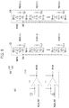
- FIG. 1 is a circuit diagram illustrating a delay cell 100 in accordance with an embodiment of the present invention.
- the delay cell 100 may be formed of a unit delay UD including first to third delay elements ND 1 to ND 3 coupled in series.
- FIG. 1 shows a case where three delay elements ND 1 to ND 3 are coupled in series, the present invention is not limited to that specific arrangement; the number of delay elements that are coupled in series within one unit delay UD may vary depending on design.
- a first delay element ND 1 may be realized as a NAND gate including a first input terminal for receiving a power source voltage VDD and a second input terminal for receiving an input signal IN.
- the first delay element ND 1 may receive an input signal IN and invert the input signal IN and delay the inverted input signal for a set time.
- a second delay element ND 2 may be realized as a NAND gate including a first input terminal for receiving a delay control signal S 1 and a second input terminal for receiving an output OUT_ND 1 of the first delay element ND 1 .
- the delay control signal S 1 may be activated to a logic high level to operate the delay cell 100 .
- the second delay element ND 2 may receive the output OUT_ND 1 of the first delay element ND 1 , and invert and delay it for a set time.
- the third delay element ND 3 may be realized as a NAND gate including a first input terminal for receiving the power source voltage VDD and a second input terminal for receiving an output OUT_ND 2 of the second delay element ND 2 .
- the third delay element ND 3 may receive the output OUT_ND 2 of the second delay element ND 2 , and invert and delay it for a set time.
- the first to third delay elements ND 1 to ND 3 may be realized as inverting devices (for example, a NAND gate or an inverter).
- the delay cell 100 may further include an inverting device ND 4 that receives an output OUT_ND 3 of the third delay element ND 3 , and inverts and delays it in order to delay the input signal IN without phase inversion and provide it as an output signal OUT.
- the inverting device ND 4 may be realized as a NAND gate including a first input terminal for receiving the power source voltage VDD and a second input terminal for receiving the output OUT_ND 3 of the third delay element ND 3 .
- the delay cell 100 in accordance with an embodiment of the present invention may further include at least one three-phase inverter TIV 1 and TIV 2 coupled in parallel to at least one delay element among the first to third delay elements ND 1 to ND 3 .
- FIG. 1 shows a first three-phase inverter TIV 1 and a second three-phase inverter TIV 2 that are coupled in parallel to the first delay element ND 1 and the third delay element ND 3 , respectively.
- the first three-phase inverter TIV 1 may be coupled between the second input terminal and the output terminal of the first delay element ND 1
- the second three-phase inverter TIV 2 may be coupled between the second input terminal and the output terminal of the second delay element ND 3 .
- FIG. 1 shows two three-phase inverters (the first three-phase inverter TIV 1 and the second three-phase inverter TIV 2 ), the present disclosure is not limited thereto. That is, the number of the three-phase inverters may vary depending on design.
- the first and second three-phase inverters TIV 1 and TIV 2 may have a primary (or first) control terminal for receiving a first bias voltage NBIAS that compensates for variation of the power source voltage VDD and a secondary (or second) control terminal for receiving a second bias voltage PBIAS for compensating for variation of the ground voltage VSS.
- the first bias voltage NBIAS may move in a direction opposite to the variation of the power source voltage VDD. In other words, when the voltage level of the power source voltage VDD increases above a target voltage, the voltage level of the first bias voltage NBIAS may decrease. When the voltage level of the power source voltage VDD is decreased lower than the target voltage, the voltage level of the first bias voltage NBIAS may increase.
- the second bias voltage PBIAS may move in the opposite direction to the variation of the ground voltage VSS. In other words, when the voltage level of the ground voltage VSS increases above the target voltage, the voltage level of the second bias voltage PBIAS may decrease. When the voltage level of the ground voltage VSS is decreased lower than the target voltage, the voltage level of the second bias voltage PBIAS may increase.
- the first three-phase inverter TIV 1 and the second three-phase inverter TIV 2 may operate in a path through which the input signal IN passes, and thus the generation of jitter may be suppressed by compensating a driving force that varies as the voltage levels of the power source voltage VDD and the ground voltage VSS are changed.
- the delay cell 100 may further include a voltage generation circuit 200 , such as that shown in FIG. 2 , for generating the first bias voltage NBIAS and the second bias voltage PBIAS.
- the voltage generation circuit 200 may be provided within or externally to the delay cell 100 .
- FIG. 2 is a circuit diagram illustrating the voltage generation circuit 200 for generating the first bias voltage NBIAS and the second bias voltage PBIAS shown in FIG. 1 .
- the voltage generation circuit 200 may include a first operational amplifier OP 1 , a second operational amplifier OP 2 , and first to fourth resistors R 1 to R 4 .
- the first operational amplifier OP 1 may receive a first reference voltage NBIAS_REF at a positive (+) terminal and output the first bias voltage NBIAS at an output terminal.
- the first resistor R 1 may be coupled between a power source voltage VDD terminal and a negative ( ⁇ ) terminal of the first operational amplifier OP 1 .
- the second resistor R 2 may be coupled between a negative ( ⁇ ) terminal and the output terminal of the first operational amplifier OP 1 .
- the first operational amplifier OP 1 may have an amplification gain ( ⁇ R 2 /R 1 ) based on the resistance ratio of the first resistor R 1 and the second resistor R 2 .
- the first reference voltage NBIAS_REF and the second reference voltage PBIAS_REF may be voltages having a uniform voltage level regardless of the variation of the voltage.
- the voltage generation circuit 200 may generate the first bias voltage NBIAS by amplifying the variation of the power source voltage VDD with respect to the first reference voltage NBIAS_REF at the ratio ⁇ R 2 /R 1 and, generate the second bias voltage PBIAS by amplifying the variation of the ground voltage VSS with respect to the second reference voltage PBIAS_REF at the ratio ⁇ R 4 /R 3 . Therefore, the first bias voltage NBIAS may move in a direction opposite to the variation of the power source voltage VDD, and the second bias voltage PBIAS may move in the opposite direction to the variation of the ground voltage VSS.
- FIG. 3 is an equivalent circuit diagram illustrating the delay cell 100 shown in FIG. 1 in accordance with an embodiment of the present invention.
- the delay cell 100 may include first to third delay elements ND 1 to ND 3 , an inverting device ND 4 , and first and second three-phase inverters TIV 1 and TIV 2 .
- the first three-phase inverter TIV 1 may include first to fourth transistors MP 1 , MP 2 , MN 1 , and MN 2 that are coupled in series between the power source voltage VDD terminal and the ground voltage VSS terminal.
- the first and second transistors MP 1 and MP 2 may be realized as PMOS (P-type Metal Oxide Semiconductor) transistors
- the third and fourth transistors MN 1 and MN 2 may be realized as NMOS (N-type Metal Oxide Semiconductor) transistors.
- the first transistor MP 1 may receive the second bias voltage PBIAS through a gate
- a gate of the fourth transistor MN 2 may receive the first bias voltage NBIAS.
- the gates of the second and third transistors MP 2 and MN 1 may be coupled to a second input terminal of the first delay element ND 1 to receive the input signal IN.
- the drains of the second and third transistors MP 2 and MN 1 that are coupled in common may be coupled to the output OUT_ND 1 of the first delay element ND 1 .
- the second three-phase inverter TIV 2 may include fifth to eighth transistors MP 3 , MP 4 , MN 3 and MN 4 that are coupled in series between the power source voltage VDD terminal and the ground voltage VSS terminal.
- the fifth and sixth transistors MP 3 and MP 4 may be realized as PMOS transistors
- the seventh and eighth transistors MN 3 and MN 4 may be realized as NMOS transistors.
- the fifth transistor MP 3 may receive the second bias voltage PBIAS through a gate
- a gate of the eighth transistor MN 4 may receive the first bias voltage NBIAS.
- the gates of the sixth and seventh transistors MP 4 and MN 3 may be coupled to the second input terminal of the third delay element ND 3 to receive the output OUT_ND 2 of the second delay element ND 2 .
- the drains of the sixth and seventh transistors MP 4 and MN 3 that are coupled in common may be coupled to the output OUT_ND 3 of the third delay element ND 3 .
- a compensation operation of a three-phase inverter in accordance with an embodiment of the present invention is described below with reference to FIGS. 3 to 7 .
- FIGS. 4 and 5 illustrate a circuit diagram and a timing diagram for explaining compensation operations of the first three-phase inverter TIV 1 and the second three-phase inverter TIV 2 based on the variation of the power source voltage VDD, respectively.
- FIGS. 6 and 7 illustrate a circuit diagram and a timing diagram for explaining the compensation operations of the first three-phase inverter TIV 1 and the second three-phase inverter TIV 2 based on the variation of the ground voltage VSS.
- the first to third delay elements ND 1 to ND 3 and the inverting device ND 4 have the same delay amount tD 1 .
- the present invention is not limited to this specific arrangement. In another embodiment, different delay elements may have different delay amounts.
- the first delay element ND 1 may invert and delay the input signal IN for a time tD 1 , which may be predetermined, and output the inverted and delayed signal as output OUT_ND 1 .
- the second delay element ND 2 may invert and delay the output OUT_ND 1 of the first delay element ND 1 for the time tD 1 and then output it as output OUT_ND 2 .
- the third delay element ND 3 may invert and delay the output OUT_ND 2 of the second delay element ND 2 for the time tD 1 and then output it as output OUT_ND 3 .
- the inverting device ND 4 may output an output signal OUT by inverting the output OUT_ND 3 of the third delay element ND 3 .
- the logic high level of the input signal IN may be increased by a specific level, and the driving force of the third transistor MN 1 may become stronger than that of the second transistor MP 2 .
- the output OUT_ND 1 may transition to a logic low level more quickly.
- the voltage generation circuit 200 may decrease and output the first bias voltage NBIAS, as the power source voltage VDD is increased. Accordingly, the driving force of the fourth transistor MN 2 may become weaker than that of the first transistor MP 1 , thus reducing the amount of current flowing through the first three-phase inverter TIV 1 .
- the delay amount tD 1 of the output OUT_ND 1 with respect to the input signal IN may be maintained and corrected to a uniform level, that is, kept robust to power noise.
- the driving force of the seventh transistor MN 3 may become stronger than that of the sixth transistor MP 4 , and thus the output OUT_ND 3 may transition to a logic low level more quickly.
- the driving force of the eighth transistor MN 4 may become weaker than that of the fifth transistor MP 3 , and thus the amount of current flowing through the second three-phase inverter TIV 2 may be reduced.
- the delay amount tD 1 of the output OUT_ND 3 with respect to the input signal i.e., the output OUT_ND 2
- the delay amount tD 1 of the output OUT_ND 3 with respect to the input signal i.e., the output OUT_ND 2
- the delay amount tD 1 of the output OUT_ND 3 with respect to the input signal i.e., the output OUT_ND 2
- the logic high level of the input signal IN may decrease by a specific level and the driving force of the third transistor MN 1 may become weak.
- the output OUT_ND 1 may transition to a logic low level more slowly.
- the voltage generation circuit 200 may increase and output the first bias voltage NBIAS, as the power source voltage VDD is decreased. Accordingly, the driving force of the fourth transistor MN 2 may become stronger than that of the first transistor MP 1 , and thus the amount of current flowing through the first three-phase inverter TIV 1 may be increased.
- the delay amount tD 1 of the output OUT_ND 1 with respect to the input signal IN may be maintained and corrected to a uniform level, that is, kept robust to power noise.
- the driving force of the seventh transistor MN 3 may become weaker than that of the sixth transistor MP 4 , and the output OUT_ND 3 may transition to a logic low level more slowly.
- the driving force of the eighth transistor MN 4 may become stronger than that of the fifth transistor MP 3 , and thus the amount of current flowing through the second three-phase inverter TIV 2 may be increased.
- the delay amount tD 1 of the output OUT_ND 3 with respect to the input signal i.e., the output OUT_ND 2
- the delay amount tD 1 of the output OUT_ND 3 with respect to the input signal i.e., the output OUT_ND 2
- the delay amount tD 1 of the output OUT_ND 3 with respect to the input signal i.e., the output OUT_ND 2
- the delay amount tD 1 of the output OUT_ND 1 with respect to the input signal IN may be maintained and corrected to a uniform level, that is, kept robust to power noise.
- the driving force of the sixth transistor MP 4 may become weak, and the output OUT_ND 3 may transition to a logic high level more slowly.
- the driving force of the fifth transistor MP 3 may become strong, and the amount of current flowing through the second three-phase inverter TIV 2 may be increased.
- the delay amount tD 1 of the output OUT_ND 3 with respect to the input signal i.e., the output OUT_ND 2
- the delay amount tD 1 of the output OUT_ND 3 with respect to the input signal i.e., the output OUT_ND 2
- the delay amount tD 1 of the output OUT_ND 3 with respect to the input signal i.e., the output OUT_ND 2
- the delay amount tD 1 of the output OUT_ND 3 with respect to the input signal i.e., the output OUT
- the logic low level of the input signal IN may be decreased by a set level and the driving force of the second transistor MP 2 may become stronger than that of the third transistor MN 1 , and thus the output OUT_ND 1 may transition to a logic high level more quickly.
- the voltage generation circuit 200 may increase and output the second bias voltage PBIAS as the ground voltage VSS is decreased. Accordingly, the driving force of the first transistor MP 1 may become weaker than that of the fourth transistor MN 2 , and the amount of current flowing through the first three-phase inverter TIV 1 may be decreased.
- the delay amount tD 1 of the output OUT_ND 1 with respect to the input signal IN may be maintained and corrected to a uniform level, that is, kept robust to power noise.
- the driving force of the sixth transistor MP 4 may become strong, and the output OUT_ND 3 may transition to a logic high level more quickly.
- the driving force of the fifth transistor MP 3 may become weaker than that of the eighth transistor MN 4 , and the amount of current flowing through the second three-phase inverter TIV 2 may be decreased.
- the delay amount tD 1 of the output OUT_ND 3 with respect to the input signal i.e., the output OUT_ND 2
- the delay amount tD 1 of the output OUT_ND 3 with respect to the input signal i.e., the output OUT_ND 2
- the delay amount tD 1 of the output OUT_ND 3 with respect to the input signal i.e., the output OUT_ND 2
- the generation of jitter may be suppressed by compensating the driving force that varies as the voltage levels of the power source voltage VDD and the ground voltage VSS are changed.
- the first operational amplifier OP 1 and the second operational amplifier OP 2 of the voltage generation circuit 200 may be set to have a higher amplification gain.
- the first bias voltage NBIAS and the second bias voltage PBIAS may be set to be included in the operating region of an NMOS/PMOS transistor.
- the delay line 300 may include a plurality of first delay elements ND 11 to ND 1 n , a plurality of second delay elements ND 21 to ND 2 n , and a plurality of third delay elements ND 31 to ND 3 n .
- the first to third delay elements ND 11 to ND 1 n , ND 21 to ND 2 n and ND 31 to ND 3 n may correspond to each other, and the corresponding first to third delay elements may form one unit delay UD.
- the delay line 300 may include a plurality of unit delays UD 1 to UDn.
- the first delay elements ND 11 to ND 1 n may be coupled in series to receive the input signal IN based on a plurality of delay control signals S ⁇ 1 : n >.
- each of the first delay elements ND 11 to ND 1 n may be realized as a NAND gate that receives a corresponding signal among the delay control signals S ⁇ 1 : n > through a first input terminal and receive an output of a preceding stage through a second input terminal.
- the first delay element ND 11 of the first stage may receive the input signal IN through the second input terminal.
- the first delay elements ND 11 to ND 1 n may invert the input signal IN and delay the inverted input signal for a set time based on the delay control signals S ⁇ 1 : n>.
- the second delay elements ND 21 to ND 2 n may be coupled in series to output an output signal OUTB.
- each of the second delay elements ND 21 to ND 2 n may be realized as a NAND gate that receives the output of the preceding stage through the first input stage and receives the output of the corresponding third delay element through the second input terminal.
- the second delay element ND 2 n of the last stage may receive the power source voltage VDD through the first input terminal and the second delay element ND 21 at the first stage may receive the output signal OUTB.
- the third delay elements ND 31 to ND 3 n may couple the first delay elements ND 11 to ND 1 n to the second delay elements ND 21 to ND 2 n respectively, based on inverted delay control signals SB ⁇ 2 : n > that are generated by inverting a plurality of delay control signals S ⁇ 2 : n >.
- each of the third delay elements ND 31 to ND 3 n may be realized as a NAND gate that receives a corresponding signal among the inverted delay control signals SB ⁇ 2 : n > through the first input terminal, and receives the output of the first delay element.
- the third delay element ND 31 of the first stage may receive the inverted delay control signal SB ⁇ 2 > through the first input terminal.
- the third delay element ND 32 of the second stage may receive the inverted delay control signal SB ⁇ 3 > through the first input terminal.
- the third delay element ND 3 n of the last stage may receive the power source voltage VDD through the first input terminal.
- the third delay elements ND 31 to ND 3 n may delay the output of the first delay elements ND 11 to ND 1 n for a set time based on the inverted delay control signals SB ⁇ 2 : n > and provide the delayed signal to the second input terminals of the second delay elements ND 21 to ND 2 n.
- first to third delay elements ND 11 to ND 1 n , ND 21 to ND 2 n and ND 31 to ND 3 n may be realized as an inverting device (for example, a NAND gate or an inverter).
- the delay line 300 may further include an inverting device ND 41 for receiving the output signal OUTB of the second delay elements ND 21 to ND 2 n , and inverting and outputting it as output OUT.
- the inverting device ND 41 may be realized as a NAND gate that receives the power source voltage VDD through the first input terminal and receives the output OUTB of the third delay element ND 31 to ND 3 n through the second input terminal.
- the delay line 300 in accordance with an embodiment of the present invention may include a plurality of first three-phase inverters TIV 11 to TIV 1 n that are coupled in parallel with the first delay elements ND 11 to ND 1 n .
- the first three-phase inverters TIV 11 to TIV 1 n may receive a plurality of first bias voltages NBIAS ⁇ 1 : n > for compensating for the variation of the power source voltage VDD through a first control terminal, and receive a plurality of second bias voltages PBIAS ⁇ 1 : n > for compensating for the variation of the ground voltage VSS through a second control terminal.
- the first three-phase inverters TIV 11 to TIV 1 n may be coupled between the second input terminal and the output terminal of the first delay elements ND 11 to ND 1 n .
- the first three-phase inverters TIV 11 to TIV 1 n may have substantially the same structure as the first three-phase inverter TIV 1 described above with reference to FIGS. 3 to 7 .
- the delay line 300 in accordance with an embodiment of the present invention may include a plurality of second three-phase inverters TIV 21 to TIV 2 n and a plurality of third three-phase inverters TIV 31 to TIV 3 n that are coupled in parallel with the second delay elements ND 21 to ND 2 n .
- the second three-phase inverters TIV 21 to TIV 2 n may be coupled in parallel between the first input terminal and the output terminal of the second delay elements ND 21 to ND 2 n to receive a plurality of first bias voltages NBIAS ⁇ 2 : n > for compensating for the variation of the power source voltage VDD through the first control terminal and to receive a plurality of second bias voltages PBIAS ⁇ 2 : n > for compensating for the variation of the ground voltage VSS through the second control terminal.
- the third three-phase inverters TIV 31 to TIV 3 n may be coupled in parallel between the second input terminal and an output terminal of the second delay elements ND 21 to ND 2 n to receive inverted delay control signals SB ⁇ 2 : n > through the first control terminal, and receive a plurality of delay control signals S ⁇ 2 : n > through the second control terminal.
- the third three-phase inverters TIV 31 to TIV 3 n may be turned on/off based on the delay control signals S ⁇ 2 : n > and the inverted delay control signals SB ⁇ 2 : n >.
- Each of the second three-phase inverters TIV 21 to TIV 2 n and the third three-phase inverters TIV 31 to TIV 3 n may have substantially the same structure as the second three-phase inverters TIV 2 described above with reference to FIGS. 3 to 7 .
- the second three-phase inverter TIV 2 n of the last stage among the second three-phase inverters TIV 21 to TIV 2 n may receive the ground voltage VSS and the power source voltage VDD through the first and second control terminals, respectively.
- the third three-phase inverter TIV 3 n of the last stage among the third three-phase inverters TIV 31 to TIV 3 n may receive the power source voltage VDD and the ground voltage VSS through the first and second control terminals, respectively. Therefore, whereas the second three-phase inverter TIV 2 n of the last stage maintains a turn-off state, the third-stage three-phase inverter TIV 3 n of the last stage may maintain a turn-on state.
- the delay line 300 may include a voltage compensation circuit 400 , such as that shown in FIG. 9 , for generating a plurality of first bias voltages NBIAS ⁇ 1 : n > and a plurality of second bias voltages PBIAS ⁇ 1 : n >.
- the voltage compensation circuit 400 may be provided within or externally to the delay line 300 .
- FIG. 9 is a circuit diagram illustrating the voltage compensation circuit 400 for generating a plurality of first bias voltages NBIAS ⁇ 1 : n > and a plurality of second bias voltages PBIAS ⁇ 1 : n > shown in FIG. 8 .
- FIG. 10 is a logic table explaining an operation of the voltage compensation circuit 400 shown in FIG. 9 .
- the voltage compensation circuit 400 may include a voltage generation circuit 410 and a voltage output circuit 430 .
- the voltage generation circuit 410 may generate a first base voltage NBASE by amplifying the variation of the power source voltage VDD with respect to the first reference voltage NBIAS_REF at a ratio ⁇ R 2 /R 1 , and generate a second base voltage PBASE by amplifying the variation of the ground voltage VSS with respect to the two reference voltages PBIAS_REF at a ratio ⁇ R 4 /R 3 .
- the voltage generation circuit 410 may have substantially the same structure as the voltage generation circuit 200 of FIG. 2 .
- the voltage output circuit 430 may output the first base voltage NBASE as at least one among the first bias voltages NBIAS ⁇ 1 : n > and output the second base voltage PBASE as at least one among the second bias voltages PBIAS ⁇ 1 : n >, based on the delay control signals S ⁇ 1 : n > and the inverted delay control signals SB ⁇ 1 : n>.
- the voltage output circuit 430 may include a first voltage output unit 432 and a second voltage output unit 434 .
- the first voltage output unit 432 may select first base voltage NBASE or the ground voltage VSS and output the first bias voltages NBIAS ⁇ 1 : n > based on the delay control signals S ⁇ 1 : n > and the inverted delay control signals SB ⁇ 1 : n >.
- the first voltage output unit 432 may include a plurality of first transferors TG 11 to TG 1 n that respectively output a plurality of first bias voltages NBIAS ⁇ 1 : n >.
- the delay control signals S ⁇ 1 : n > are activated, the first transferors TG 11 to TG 1 n may output the first base voltage NBASE as the first bias voltages NBIAS ⁇ 1 : n >.
- the inverted delay control signals SB ⁇ 1 : n > are activated, the first transferors TG 11 to TG 1 n may output the ground voltage VSS as the first bias voltages NBIAS ⁇ 1 : n>.
- the second voltage output unit 434 may select the second base voltage PBASE or the power source voltage VDD based on the delay control signals S ⁇ 1 : n > and the inverted delay control signals SB ⁇ 1 : n >, and output the second bias voltages PBIAS ⁇ 1 : n >.
- the second voltage output unit 434 may include a plurality of second transferors TG 21 to TG 2 n that respectively output a plurality of second bias voltages PBIAS ⁇ 1 : n >.
- the delay control signals S ⁇ 1 : n > are activated, the second transferors TG 21 to TG 2 n may output the second base voltage PBASE as the second bias voltages PBIAS ⁇ 1 : n >.
- the inverted delay control signals SB ⁇ 1 : n > are activated, the second transferors TG 21 to TG 2 n may output the power source voltage VDD as the second bias voltages PBIAS ⁇ 1 : n>.
- the delay control signals S ⁇ 1 : n > may be the signals that are set to determine the number of unit delays to be used among the unit delays UD 1 to UD n .
- the delay control signals S ⁇ 1 : n > may be formed of a thermometer code (which is a unary code).
- the delay control signals S ⁇ 1 : n > may have an initial value of ‘1000 . . . 0000’.
- the delay control signals S ⁇ 1 : n > may be increased to ‘1100 . . . 0000’, ‘1110 . . . 0000’, ‘111111 . . . 1111’.
- the voltage compensation circuit 400 may output the first and second base voltages NBASE and PBASE as the first and second bias voltages NBIAS ⁇ 1 > and PBIAS ⁇ 1 >, respectively, based on the delay control signal S ⁇ 1 > that is activated to a logic high level.
- the voltage compensation circuit 400 may fix the remaining first bias voltages NBIAS ⁇ 2 : n > to the ground voltage VSS and output them, and the voltage compensation circuit 400 may fix the remaining second bias voltages PBIAS ⁇ 2 : n > to the power source voltage VDD and output them.
- the voltage compensation circuit 400 may output the first and second base voltages NBASE and PBASE as the first and second bias voltages NBIAS ⁇ 1 : n > and PBIAS ⁇ 1 : n >, respectively, based on the delay control signals S ⁇ 1 : n > that are activated to a logic high level.
- the voltage compensation circuit 400 may generate the first bias voltages NBIAS ⁇ 1 : n > by amplifying the variation of the power source voltage VDD with respect to the first reference voltage NBIAS_REF at a ratio ⁇ R 2 /R 1 , and generate the second bias voltages PBIAS ⁇ 1 : n > by amplifying the variation of the ground voltage VSS with respect to the second reference voltage PBIAS_REF at a ratio ⁇ R 4 /R 3 .
- FIGS. 11A to 11C are circuit diagrams illustrating an operation of the delay line shown in FIG. 8 .
- the delay control signals S ⁇ 1 : n > are ‘1000 . . . 0000’ is shown.
- the delay control signal S ⁇ 1 > may be activated to a logic high level, and the remaining delay control signals S ⁇ 2 : n > may be deactivated to a logic low level.
- the inverted delay control signal SB ⁇ 1 > may be activated to a logic low level, and the remaining inverted delay control signals SB ⁇ 2 : n > may be deactivated to a logic high level.
- the shadowed first delay element ND 11 of the first stage may operate as a delay element (i.e., an inverter), and the remaining first delay elements ND 12 to ND 1 n may provide an output fixed to a logic high level.
- the shadowed third delay element ND 31 of the first stage may operate as a delay element, and the remaining third delay elements ND 32 to ND 3 n may provide an output fixed to a logic low level.
- the remaining second delay elements ND 22 to ND 2 n except for the shadowed second delay element ND 21 , of the first stage may provide an output fixed to a logic high level.
- the shadowed second delay element ND 21 of the first stage may operate as a delay element.
- the first unit delay UD 1 may operate to delay the input signal IN and provide it as the output signal OUTB.
- the voltage compensation circuit 400 may output the first and second base voltages NBASE and PBASE as the first and second bias voltages NBIAS ⁇ 1 > and PBIAS ⁇ 1 >, respectively, and output the remaining first bias voltages NBIAS ⁇ 2 : n > after fixing them to the ground voltage VSS and output the remaining second bias voltages PBIAS ⁇ 2 : n > after fixing them to the power source voltage VDD. Therefore, the shadowed first three-phase inverter TIV 11 of the first stage and the shadowed third three-phase inverters TIV 31 to TIV 3 n may be activated and operated.
- the first three-phase inverter TIV 11 may operate in the path through which the input signal IN passes and thus the generation of jitter may be suppressed by compensating the driving force that varies as the voltage levels of the power source voltage VDD and the ground voltage VSS are changed.
- the delay line 300 shown in FIG. 11 A further includes an inverting device ND 41 for receiving the output signal OUTB of the first unit delay UD 1 , and inverting it and outputting it as output OUT.
- the inverting device ND 41 may be realized as a NAND gate that receives the power source voltage VDD through the first input terminal and receives the output OUTB through the second input terminal.
- the shadowed first delay elements ND 11 to ND 13 may each operate as a delay element (i.e., an inverter), and the remaining first delay elements ND 14 to ND 1 n may provide an output fixed to a logic high level.
- the shadowed third delay element ND 33 which corresponds to the last, i.e., ND 13 , among the first delay elements ND 11 to ND 13 , may operate as a delay element, and the third delay elements ND 31 and ND 32 , which correspond to ND 11 and ND 12 , may provide an output fixed to a logic high level, and the remaining third delay elements ND 34 to ND 3 n may provide an output fixed to a logic low Level.
- the shadowed second delay elements ND 21 to ND 23 which correspond to the first delay elements ND 11 to ND 13 , may operate as delay elements, and the remaining second delay elements ND 24 to ND 2 n may provide an output fixed to a logic high level.
- the first to third unit delays UD 1 to UD 3 may operate to delay the input signal IN and provide it as the output signal OUTB.
- the voltage compensation circuit 400 may output the first and second base voltages NBASE and PBASE as the first and second bias voltages NBIAS ⁇ 1 : 3 > and PBIAS ⁇ 1 : 3 >, respectively. Therefore, the shadowed first three-phase inverters TIV 11 to TIV 13 , the shadowed second three-phase inverters TIV 21 and TIV 22 , and the shadowed third three-phase inverters TIV 33 to TIV 3 n may be activated and operate.
- the first three-phase inverters TIV 11 to TIV 13 and the second three-phase inverters TIV 21 and TIV 22 may operate in a path through which the input signal IN passes and thus the generation of jitter may be suppressed by compensating the driving force that varies as the voltage levels of the power source voltage VDD and the ground voltage VSS are changed.
- the delay line 300 shown in FIG. 11B further includes an inverting device ND 41 for receiving the output signal OUTB of the first to third unit delay UD 1 to UD 3 , and inverting it and outputting it as output OUT.
- the inverting device ND 41 may be realized as a NAND gate that receives the power source voltage VDD through the first input terminal and receives the output OUTB through the second input terminal.
- all of the shadowed first delay elements ND 11 to ND 1 n may operate as delay elements (i.e., inverters). Also, only the shadowed third delay element ND 3 n of the last stage may operate as a delay element, and the remaining third delay elements ND 31 to ND 3 n - 1 may provide an output fixed to a logic high level. Accordingly, all of the shadowed second delay elements ND 21 to ND 2 n may operate as delay elements. In short, the first to n th unit delays UD 1 to UDn may operate to delay the input signal IN and provide it as the output signal OUTB.
- the voltage compensation circuit 400 may output the first and second base voltages NBASE and PBASE as all the first and second bias voltages NBIAS ⁇ 1 : n > and PBIAS ⁇ 1 : n >. Therefore, all of the shadowed first three-phase inverters TIV 11 to TIV 1 n , the shadowed second three-phase inverters TIV 21 to TIV 2 n - 1 except for those of the last stage, and the shadowed third-stage three-phase inverter TIV 3 n of the last stage may be activated and operate.
- the first three-phase inverters TIV 11 to TIV 1 n and the second three-phase inverters TIV 21 to TIV 2 n - 1 may operate in a path through which the input signal IN passes and thus the generation of jitter may be suppressed by compensating the driving force that varies as the voltage levels of the power source voltage VDD and the ground voltage VSS are changed.
- the delay line 300 shown in FIG. 11 C further includes an inverting device ND 41 for receiving the output signal OUTB of the first to nth unit delays UD 1 to UDn, and inverting it and outputting it as output OUT.
- the inverting device ND 41 may be realized as a NAND gate that receives the power source voltage VDD through the first input terminal and receives the output OUTB through the second input terminal.
- the second three-phase inverters TIV 21 to TIV 2 n and the third three-phase inverters TIV 31 to TIV 3 n may correspond to each other, and one of the corresponding second three-phase inverter and the corresponding third three-phase inverter may be turned on.
- FIG. 12 is a block diagram illustrating a delay locked loop (DLL) circuit 500 including a delay line in accordance with an embodiment of the present invention.
- DLL delay locked loop
- the delay locked loop circuit 500 may include a delay line 510 , a replica delayer 520 , a phase detector 530 , and a delay controller 540 .
- the delay line 510 may include a plurality of unit delays, and output a delay clock INCLK by selecting the number of unit delays to be used based on the delay control signals S ⁇ 1 : n > and delaying an external clock EXTCLK for a set time.
- the delay line 510 may control the driving force of at least one delay element of the unit delays that are selected based on the first bias voltages NBIAS ⁇ 1 : n > and the second bias voltages PBIAS ⁇ 1 : n >.
- the delay line 510 may have substantially the same structure as the delay line 300 shown in FIG. 8 .
- the replica delayer 520 may be a circuit formed to have the same delay condition as an actual clock path (which is also referred to as a tAC path) through which the delay clock INCLK is transferred to the final data output terminal of the semiconductor device.
- the replica delayer 520 may receive the delay clock INCLK and generate a feedback clock FBCLK.
- the feedback clock FBCLK may have the same phase as that of the clock transferred to the final data output terminal of the semiconductor device.
- the phase detector 530 may generate a phase comparison signal PD_DET by comparing the phase of the external clock EXTCLK and the phase of the feedback clock FBCLK with each other.
- the delay control unit 540 may include a plurality of delay control signals S ⁇ 1 : n > for selecting the number of the unit delays that are used in the delay line 510 based on the phase comparison signal PD_DET inputted from the phase detector 530 .
- the delay controller 540 may include the structure of the voltage compensation circuit 400 of FIG. 9 .
- the delay controller 540 may generate a plurality of first bias voltages NBIAS ⁇ 1 : n > for compensating for the variation of the power source voltage VDD and generate a plurality of second bias voltages PBIAS ⁇ 1 : n > for compensating for the variation of the ground voltage VSS based on the delay control signals S ⁇ 1 : n>.
- the delay locked loop circuit 500 may adjust the delay amount of the delay clock INCLK so that the phase of the clock signal used in the final data input/output terminal of the semiconductor device is synchronized with the external clock EXTCLK.
- the delay locked loop circuit 500 in accordance with an embodiment of the present invention may suppress the generation of jitter by compensating the driving force that varies as the voltage levels of the power source voltage VDD and the ground voltage VSS are changed.
- delay lines and a delay line including the delay cells are robust to power noise, it is possible to more precisely control the delay time of an input signal.
- logic gates and transistors illustrated in the above embodiments may be realized in different positions and types according to the polarity of input signals.
Landscapes
- Physics & Mathematics (AREA)
- Nonlinear Science (AREA)
- Pulse Circuits (AREA)
Abstract
Description
Claims (22)
Applications Claiming Priority (2)
| Application Number | Priority Date | Filing Date | Title |
|---|---|---|---|
| KR1020180168379A KR102581085B1 (en) | 2018-12-24 | 2018-12-24 | Delay cell and delay line having the same |
| KR10-2018-0168379 | 2018-12-24 |
Publications (2)
| Publication Number | Publication Date |
|---|---|
| US20200204168A1 US20200204168A1 (en) | 2020-06-25 |
| US10833662B2 true US10833662B2 (en) | 2020-11-10 |
Family
ID=71097953
Family Applications (1)
| Application Number | Title | Priority Date | Filing Date |
|---|---|---|---|
| US16/578,812 Active US10833662B2 (en) | 2018-12-24 | 2019-09-23 | Delay cell and delay line having the same |
Country Status (3)
| Country | Link |
|---|---|
| US (1) | US10833662B2 (en) |
| KR (1) | KR102581085B1 (en) |
| CN (1) | CN111355486B (en) |
Cited By (1)
| Publication number | Priority date | Publication date | Assignee | Title |
|---|---|---|---|---|
| US20240085939A1 (en) * | 2022-09-14 | 2024-03-14 | SK Hynix Inc. | Clock generating circuit and clock distribution network and semiconductor apparatus including the clock generating circuit |
Families Citing this family (1)
| Publication number | Priority date | Publication date | Assignee | Title |
|---|---|---|---|---|
| US11335396B1 (en) * | 2020-11-19 | 2022-05-17 | Micron Technology, Inc. | Timing signal delay for a memory device |
Citations (3)
| Publication number | Priority date | Publication date | Assignee | Title |
|---|---|---|---|---|
| US20130051166A1 (en) * | 2011-08-23 | 2013-02-28 | Micron Technology, Inc. | Apparatuses and methods for compensating for power supply sensitivities of a circuit in a clock path |
| US8436670B2 (en) * | 2011-01-13 | 2013-05-07 | Micron Technology, Inc. | Power supply induced signal jitter compensation |
| US20170170646A1 (en) | 2014-09-11 | 2017-06-15 | Intel Corporation | Back power protection circuit |
Family Cites Families (6)
| Publication number | Priority date | Publication date | Assignee | Title |
|---|---|---|---|---|
| JP3637706B2 (en) * | 1996-11-27 | 2005-04-13 | ソニー株式会社 | Digital delay circuit and digitally controlled oscillation circuit using the same |
| KR100540930B1 (en) * | 2003-10-31 | 2006-01-11 | 삼성전자주식회사 | Delay Synchronous Loop Circuit |
| WO2007008579A2 (en) * | 2005-07-08 | 2007-01-18 | Zmos Technology, Inc. | Source transistor configurations and control methods |
| US20080309386A1 (en) * | 2007-06-15 | 2008-12-18 | Mosaid Technologies Incorporated | Bias generator providing for low power, self-biased delay element and delay line |
| US7948330B2 (en) * | 2009-03-19 | 2011-05-24 | Qualcomm Incorporated | Current controlled oscillator with regulated symmetric loads |
| JP6123569B2 (en) * | 2013-08-15 | 2017-05-10 | 株式会社ソシオネクスト | Voltage generation circuit and control method of voltage generation circuit |
-
2018
- 2018-12-24 KR KR1020180168379A patent/KR102581085B1/en active Active
-
2019
- 2019-09-23 US US16/578,812 patent/US10833662B2/en active Active
- 2019-11-25 CN CN201911166444.1A patent/CN111355486B/en active Active
Patent Citations (3)
| Publication number | Priority date | Publication date | Assignee | Title |
|---|---|---|---|---|
| US8436670B2 (en) * | 2011-01-13 | 2013-05-07 | Micron Technology, Inc. | Power supply induced signal jitter compensation |
| US20130051166A1 (en) * | 2011-08-23 | 2013-02-28 | Micron Technology, Inc. | Apparatuses and methods for compensating for power supply sensitivities of a circuit in a clock path |
| US20170170646A1 (en) | 2014-09-11 | 2017-06-15 | Intel Corporation | Back power protection circuit |
Cited By (2)
| Publication number | Priority date | Publication date | Assignee | Title |
|---|---|---|---|---|
| US20240085939A1 (en) * | 2022-09-14 | 2024-03-14 | SK Hynix Inc. | Clock generating circuit and clock distribution network and semiconductor apparatus including the clock generating circuit |
| US12189416B2 (en) * | 2022-09-14 | 2025-01-07 | SK Hynix Inc. | Clock generating circuit and clock distribution network and semiconductor apparatus including the clock generating circuit |
Also Published As
| Publication number | Publication date |
|---|---|
| CN111355486B (en) | 2023-07-07 |
| KR102581085B1 (en) | 2023-09-21 |
| KR20200078971A (en) | 2020-07-02 |
| CN111355486A (en) | 2020-06-30 |
| US20200204168A1 (en) | 2020-06-25 |
Similar Documents
| Publication | Publication Date | Title |
|---|---|---|
| US7634039B2 (en) | Delay-locked loop with dynamically biased charge pump | |
| US7180346B2 (en) | Duty cycle correcting circuits having a variable gain and methods of operating the same | |
| US6084452A (en) | Clock duty cycle control technique | |
| US8947141B2 (en) | Differential amplifiers, clock generator circuits, delay lines and methods | |
| US8248130B2 (en) | Duty cycle correction circuit | |
| US8988955B2 (en) | Apparatuses and methods for compensating for power supply sensitivities of a circuit in a clock path | |
| US8736313B2 (en) | Input buffer capable of expanding an input level | |
| US7570094B2 (en) | Automatic duty cycle correction circuit with programmable duty cycle target | |
| US10581419B2 (en) | Skew detection circuit and input circuit using the same | |
| US7511553B2 (en) | Current controlled level shifter with signal feedback | |
| US7142032B2 (en) | Tunable delay circuit | |
| US10833662B2 (en) | Delay cell and delay line having the same | |
| US7999611B2 (en) | Differential amplifying device | |
| US7768307B2 (en) | Current mode logic-complementary metal oxide semiconductor converter | |
| US10734985B2 (en) | Comparators for power and high-speed applications | |
| US7961026B2 (en) | Delay cell and phase locked loop using the same | |
| US20120098604A1 (en) | Ring oscillator and control method of ring oscillator | |
| US9722580B1 (en) | Process information extractor circuit | |
| KR20090067796A (en) | Unit delay cell and delay lock loop including the same |
Legal Events
| Date | Code | Title | Description |
|---|---|---|---|
| AS | Assignment |
Owner name: SK HYNIX INC., KOREA, REPUBLIC OF Free format text: ASSIGNMENT OF ASSIGNORS INTEREST;ASSIGNORS:KIM, JA-YOUNG;HAM, HYUN-JU;SIGNING DATES FROM 20190919 TO 20190920;REEL/FRAME:050459/0836 |
|
| FEPP | Fee payment procedure |
Free format text: ENTITY STATUS SET TO UNDISCOUNTED (ORIGINAL EVENT CODE: BIG.); ENTITY STATUS OF PATENT OWNER: LARGE ENTITY |
|
| STPP | Information on status: patent application and granting procedure in general |
Free format text: NOTICE OF ALLOWANCE MAILED -- APPLICATION RECEIVED IN OFFICE OF PUBLICATIONS |
|
| STPP | Information on status: patent application and granting procedure in general |
Free format text: PUBLICATIONS -- ISSUE FEE PAYMENT VERIFIED |
|
| STCF | Information on status: patent grant |
Free format text: PATENTED CASE |
|
| MAFP | Maintenance fee payment |
Free format text: PAYMENT OF MAINTENANCE FEE, 4TH YEAR, LARGE ENTITY (ORIGINAL EVENT CODE: M1551); ENTITY STATUS OF PATENT OWNER: LARGE ENTITY Year of fee payment: 4 |
|
| AS | Assignment |
Owner name: MIMIRIP LLC, TEXAS Free format text: ASSIGNMENT OF ASSIGNORS INTEREST;ASSIGNOR:SK HYNIX INC.;REEL/FRAME:067335/0246 Effective date: 20240311 Owner name: MIMIRIP LLC, TEXAS Free format text: ASSIGNMENT OF ASSIGNOR'S INTEREST;ASSIGNOR:SK HYNIX INC.;REEL/FRAME:067335/0246 Effective date: 20240311 |