US10832780B2 - Method for programming a non-volatile memory device and corresponding non-volatile memory device - Google Patents
Method for programming a non-volatile memory device and corresponding non-volatile memory device Download PDFInfo
- Publication number
- US10832780B2 US10832780B2 US16/432,369 US201916432369A US10832780B2 US 10832780 B2 US10832780 B2 US 10832780B2 US 201916432369 A US201916432369 A US 201916432369A US 10832780 B2 US10832780 B2 US 10832780B2
- Authority
- US
- United States
- Prior art keywords
- programming
- memory cells
- time interval
- memory cell
- memory
- Prior art date
- Legal status (The legal status is an assumption and is not a legal conclusion. Google has not performed a legal analysis and makes no representation as to the accuracy of the status listed.)
- Active
Links
Images


Classifications
-
- G—PHYSICS
- G11—INFORMATION STORAGE
- G11C—STATIC STORES
- G11C16/00—Erasable programmable read-only memories
- G11C16/02—Erasable programmable read-only memories electrically programmable
- G11C16/06—Auxiliary circuits, e.g. for writing into memory
- G11C16/10—Programming or data input circuits
-
- G—PHYSICS
- G11—INFORMATION STORAGE
- G11C—STATIC STORES
- G11C16/00—Erasable programmable read-only memories
- G11C16/02—Erasable programmable read-only memories electrically programmable
- G11C16/04—Erasable programmable read-only memories electrically programmable using variable threshold transistors, e.g. FAMOS
- G11C16/0408—Erasable programmable read-only memories electrically programmable using variable threshold transistors, e.g. FAMOS comprising cells containing floating gate transistors
- G11C16/0425—Erasable programmable read-only memories electrically programmable using variable threshold transistors, e.g. FAMOS comprising cells containing floating gate transistors comprising cells containing a merged floating gate and select transistor
Definitions
- Implementations and embodiments of the invention relate to a method for programming a non-volatile memory device and a corresponding non-volatile memory device.
- the logic value of a bit stored in a non-volatile memory cell is represented by the value of the threshold voltage of the floating-gate transistor of this memory cell.
- the logic value of the bit stored in this memory cell has a first value, for example, the value “1”.
- the operation of programming an erased memory cell aims to make this cell pass to a “programmed” or “written” state in which the logic value of the bit stored in this memory cell has a second value, for example, the value “0”.
- Such memory cells may be programmed by hot-electron injection or “hot carrier injection.”
- Programming by hot-electron injection has, with respect to programming via the tunnel effect, the advantage of being of short duration, generally 100 times shorter than a tunnel-effect programming operation. More precisely, the programming time of a memory cell by hot-electron injection is typically about a few microseconds compared to a few milliseconds for a tunnel-effect programming operation.
- the two transistors of the memory cell interact with a view to injecting electrical charges into the floating gate.
- the selection transistor has a conductive channel in which there forms a current that comprises electrons of high kinetic energy, i.e., so-called “hot electrons.”
- hot electrons When this current reaches the conductive channel of the state transistor, an injection region forms in which the high-energy electrons are injected into the floating gate of this transistor under the effect of a vertical electric field created by the voltage applied to the control gate of the state transistor.
- the selection transistor To obtain good injection efficiency, it is desirable for the selection transistor to operate in saturated mode (drain-source voltage very much higher than the gate-source voltage) in order for its conductive channel to have a pinch-off region in the vicinity of the injection region.
- saturated mode drain-source voltage very much higher than the gate-source voltage
- the concentration of the current in the pinch-off region promotes the appearance of electrons of high kinetic energy, the injection efficiency then being high.
- This saturated operating mode of the selection transistor is also called the weak-inversion or subthreshold mode.
- the saturated operating mode of the selection transistor is conventionally obtained by imposing a low programming current on the memory cell, by means of a current source, whereas the source-gate voltage of this selection transistor automatically adjusts to the imposed current, via a cascode effect.
- a programming duration typically a high voltage to the control gate of the state transistor (typically a voltage of about 10 volts), a voltage of about 1 volt to the gate of the selection transistor, and a voltage of about 4 to 5 volts to the drain of the state transistor.
- the various voltages applied to the memory cell during programming and in particular the voltage applied to the bit line connected to the drain of the state transistor, are delivered by a charge-pumping circuit.
- the charge pump is not capable of delivering this peak current, the voltage induced on the output of the charge pump may drop. In this case, programming cannot be guaranteed. Variations during the on-silicon fabrication of the memory cells aggravate this problem.
- the height of the programming peak is therefore a factor that affects the dimensions of the charge-pumping circuit, but also programming-operation robustness.
- One solution for decreasing the size of the charge-pumping circuit makes provision to program the memory cells using a plurality of programming pulses. This is programming parallelism.
- 64 memory cells will possibly for example, be programmed in a programming window the duration of which corresponds to two programming durations, using two consecutive programming pulses, thereby allowing 32 cells to be programmed per pulse.
- Implementations and embodiments of the invention relate to non-volatile memories, in particular embodiments, to non-volatile memories that are programmable by hot-electron injection, for example, memories comprising what are called split-gate memory cells each including a selection transistor and a floating-gate state transistor or indeed FLASH memories.
- memories comprising what are called split-gate memory cells each including a selection transistor and a floating-gate state transistor or indeed FLASH memories.
- Particular embodiments relate to memories embedded within an integrated circuit, for example, incorporating a microcontroller.
- Embodiments of the invention can decrease the required maximum programming current and thereby allow the charge pump to be better used.
- the method includes, sequentially, checking the maximum programming current before permitting the operations of programming one or more additional memory cells of the group to be triggered within a time interval during which one or more memory cells of the group are already considered as having programming operations that are triggerable.
- a method for programming a group of N memory cells of a non-volatile memory device in a programming window having a duration longer than the programming duration of a memory cell.
- the method comprises subdividing the programming window into M time intervals, M being higher than two, determining, by simulation, while taking into account a reference criterion, a programming profile including, for each time interval, a maximum number of memory cells the programming operations of which may be triggered within this time interval, (this maximum number may optionally be zero for certain of these time intervals), storing the programming profile in the memory device, and of programming the memory device in the programming window, interval wise, using the programming profile.
- the number and the duration of the time intervals in particular depend on the desired precision.
- the method comprises determining, with a reference non-volatile memory device produced in the same technology as that of the non-volatile memory device, a variation as a function of time in the programming current of a reference memory cell of the reference memory device during the programming duration.
- the reference criterion is that at the end of the intervalwise operations of programming the group of N memory cells.
- the maximum programming-current value does not exceed a fraction of the reference maximum value.
- This fraction may, for example, be about 0.75, this corresponding to a 25% decrease in the current peak.
- the step of determining by simulation advantageously comprises implementing an algorithm that will make hypotheses, carry out tests and validate the hypotheses given the reference criterion.
- the step of determining by simulation comprises ordering the memory cells of the group of N memory cells, defining at least one computational table including C coefficients that are associated with C computational times, sampling the variation as a function of time into D samples that are associated with D sampling times corresponding to D computational times, C being at least equal to the product of N multiplied by D, and ordering the M time intervals, a time interval of the sequence having a duration corresponding to DTS computational times and starting at an initial computational time, DTS being lower than D.
- a memory cell of the group of N memory cells is considered to have a programming operation that is triggerable in a time interval if, after adding the D samples to the D preceding values, and therefore an accumulation, of the coefficients of the table, which coefficients are associated with the D computational times starting at the initial computational time of this time interval, the maximum value of the coefficients of the table does not exceed the fraction of the reference maximum value whereas if the maximum value of the coefficients of the table exceeds the fraction of the reference maximum value.
- the current memory cell is considered as not having a programming operation that is triggerable in this time interval.
- the memory cell if the memory cell is considered to have a programming operation that is triggerable in the time interval, it is examined whether the programming operation of the following memory cell is triggerable in the same time interval by once again adding the D samples to the D preceding values of the coefficients of the table, which coefficients are associated with the D computational times starting at the initial computational time of the same time interval, and by determining whether the maximum value of the coefficients of the table does not exceed the fraction of the reference maximum value.
- the D samples are not added to the D preceding values of the coefficients of the table, which values are associated with the D computational times starting at the initial computational time of this time interval, but, instead, they are added to the D values of the coefficients that are associated with the D computational times starting at the initial computational time of the following time interval, and it is determined whether the programming operation of this memory cell may or may not be triggered in the following time interval by comparing the maximum value of the coefficients of the table to the fraction of the reference maximum value.
- the immediately following interval is not necessarily the right one.
- the preceding procedures are repeated until a new time interval is obtained in which the operation of programming the memory cell will be able to be triggered.
- the D samples will then actually be added to the D preceding values of the coefficients of the table, which coefficients are associated with the D computational times starting at the initial computational time of this new time interval, only when enough preceding time intervals have been rejected.
- the one or more memory cells remaining to be programmed will be subjected to the reference criterion as specified above.
- the step of determining by simulation advantageously comprises sequentially determining, memory cell after memory cell, in their order, the capacity of the programming operations of the memory cells to be triggerable in the designated time intervals, the intervals being considered sequentially in their order.
- the memory cells are, for example, programmable by hot-carrier injection.
- the memory device may be a FLASH memory device.
- Each memory cell may be a split-gate memory cell.
- the memory device may be embedded within an integrated circuit, for example, incorporating a microcontroller.
- a non-volatile memory device comprising a memory plane including memory cells, a register configured to store the programming profile obtained using the method such as defined above, and programming means configured to program a group of N memory cells in the programming window according to the programming profile.
- the programming circuit is configured to program the memory plane in groups of N memory cells.
- the memory cells are, for example, programmable by hot-carrier injection.
- the memory device may be a FLASH memory device.
- Each memory cell may be a split-gate memory cell.
- the memory device may be embedded within an integrated circuit, for example, incorporating a microcontroller.
- FIGS. 1 to 5 illustrate various implementations and embodiments of the invention.
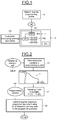
- the reference IC designates an integrated circuit here incorporating a microcontroller MC and an embedded non-volatile RAM memory device 1 .
- This device 1 includes a memory plane PM possessing memory cells CEL that are arranged in a conventional way in rows and columns, and a programming circuit MP that is configured to program these memory cells, for example, in groups of N memory cells.
- the structure of the programming circuit is conventional and known per se.
- the memory device 1 also includes a register RG that is configured to store a programming profile PRP more details on the structure of which will be given below.
- this programming profile PRP is determined by simulation in a step S 1 .
- this programming profile is stored (step S 2 ) in the register RG, so that, during the operation of the integrated circuit, and in particular of the memory device, the programming circuit MP are able to program the memory plane PM using the programming profile PRP contained in the register RG.
- the memory cells are, for example, programmable by hot-carrier injection.
- the memory device may be a FLASH memory device.
- the memory device may also be configured in such a way that each memory cell is a split-gate memory cell.
- FIGS. 2 to 4 illustrate one implementation of the step of determining the programming profile PRP by simulation.
- a window for programming N memory cells CEL is subdivided into M time intervals.
- This programming window has a duration longer than the programming duration of a memory cell. It corresponds, for example, to a programming window already used in conventional programming methods. Thus, by way of indication, when it is desired to program a group of 64 memory cells, it is possible to choose, by way of programming window, the window conventionally used to program these 64 memory cells in 2 packets of 32 memory cells. The duration of the programming window is then about two times the programming duration of a memory cell (duration of a programming pulse).
- the programming profile will comprise a maximum number of memory cells the programming operations of which will be able to be triggered simultaneously in each time interval of the programming window.
- step S 3 the programming operations of the number of cells that was determined will be triggered in succession in each time interval of the programming window, in accordance with the programming profile.
- the number M of time intervals is in particular related to the precision desired to obtain this result.
- a reference memory cell CELR is first produced in the same technology as that of the memory cells CEL of the non-volatile memory device.
- a variation F in the programming current of the reference memory cell during the programming duration DP is determined, typically by on-silicon measurements.
- this variation F as a function of time is sampled into D samples F( 1 ) . . . F(D) (step 21 ).
- D sampling times correspond to D computational times.
- the number D depends on the desired precision.
- V max of the programming current resulting from conventional operations of programming the N reference memory cells in P packets of N/P reference memory cells is also determined (step 22 ).
- the step of determining programming profiles PRP by simulation takes into account a reference criterion.
- This reference criterion is here that at the end of this step of programming the group of N memory cells interval-wise, the maximum value of the programming current does not exceed a fraction of the reference maximum value V max.
- this fraction may be about 0.75, this leading to a 25% decrease in the current peak.
- FIGS. 3 and 4 in order to schematically describe an example of a simulating algorithm allowing the programming profile PRP to be determined, i.e., allowing, in the group of N memory cells, the maximum number of memory cells the programming operations of which may be triggered in each of the M time intervals to be determined.
- the decision as to whether or not to permit the programming operation of a current memory cell to be triggered in a time interval will take into account not only the programming current, and its variation as a function of time resulting from (an)other preceding memory cell(s) optionally being programmed in this time interval or in a preceding time interval, but also the variation, as a function of time, in the programming current, in the rest of the programming window, that will result from the programming operation of this current memory cell being triggered, so that the reference criterion is respected.
- the memory cells CEL of the group of N memory cells are ordered so as to define a first memory cell CEL 1 , a current cell CEL(A), the following cell CEL(A+1) and lastly the last cell CEL(N) of the group.
- a computational table or buffer TB 1 containing C coefficients H( 1 ) . . . H(C) associated with C computational times is also defined.
- C is at least equal to the product of N multiplied by D.
- the M time intervals TS( 1 ) . . . TS(M) are also ordered.
- a time interval TS(i) has a duration corresponding to DTS computational times. Moreover, a time interval TS(i) starts at an initial computational time E(i) (counted in number of computational times).
- the length DTS of each time interval TS (counted in number of computational times) is shorter than D.
- Time intervals of 100 ns for example, maybe used.
- a second computational table (buffer) TB 2 including coefficients G( 1 ) . . . G(C) will also be defined for the sake of the example algorithm that will be described.
- step 41 it is checked whether A is higher than N, i.e., whether all of the memory cells of the group of N memory cells have been treated.
- step 50 the algorithm terminates (step 50 ).
- the content of the table TB 2 is copied to the table TB 1 and the D samples of the variation F as a function of time are added to the D values of the coefficients H(E(i)) . . . H(E(i+D)) of the table TB 1 , which coefficients are associated with the D computational times starting at the initial computational time E(i) of the time interval of rank i.
- step 43 the maximum value H max of all of the C coefficients H( 1 ) . . . H(C) of the table TB 1 is extracted from this table TB 1 .
- this value H max is compared to the fraction of the reference maximum value V max, in the present case to 3 ⁇ 4 of this value.
- a counter is associated with each time interval, the counter being intended to count the maximum number of memory cells the programming operation(s) of which is/are triggerable in this time interval, then the counter associated with this interval TSi will be incremented by 1.
- step 46 the table TB 1 will be copied to the table TB 2 and the index A will be incremented by 1 (step 47 ).
- step 44 H max remains below 3 ⁇ 4 of V max, then this means that the cell of index A+1, CEL(A+1), may also have its programming operation triggered in the interval TSi.
- step 44 relating to the cell CEL(A)
- H max is higher than or equal to 3 ⁇ 4 of V max, then this means that this cell of index A cannot have its programming operation triggered in the interval TSi.
- the index i is incremented by 1 (step 48 ), and it will be determined, by re-executing steps 42 , 43 and 44 , whether the memory cell of index A, CEL(A), may have its programming operation triggered in the following interval TS(i+1).
- step 42 since in step 42 the second table TB 2 is copied to the first table TB 1 without having carried out step 46 beforehand (copy of the table TB 1 to the table TB 2 ), the addition of the samples F( 1 ) . . . F(D) that was carried out beforehand has in fact been cancelled and this time round these samples F( 1 ) . . . F(D) are added to the D values of the coefficients H(E(i+1)) . . . H(E(i+1+D)) that are associated with the D computational times starting at the initial computational time E(i+1) of the following time interval TS(i+1) of rank i+1.
- a memory cell the programming operation of which cannot be triggered in a given interval may have its programming operation triggered in the following interval.
- the maximum number of memory cells the programming operation(s) of which may be triggered within each time interval is therefore known for each time interval.
- the programming circuit will program the memory plane in groups of N memory cells according to this programming profile.
- FIG. 5 illustrates two variations in the programming current required to program N memory cells, allowing comparison between conventional operations of programming in P packets of N/P memory cells and (interval-wise) avalanche-mode programming operations.
- the curve C 1 illustrates the variation as a function of time in the programming current for conventional operations of programming (in the programming window FP) 64 memory cells in 2 packets of 32 memory cells, the 32 memory cells being programmed simultaneously over the programming duration DP of a memory cell (duration of the programming pulse).
- the curve C 1 includes two current peaks PC the height of which is equal to 32 times the height of a current peak resulting from the operation of programming a single memory cell.
- the curve C 1 illustrates the variation as a function of time in the programming current for avalanche-mode operations of programming these 64 memory cells in the same programming window according to the programming profile obtained with the algorithm described, by way of example, with reference to FIGS. 3 and 4 .
- the programming window FP has a duration longer than the programming duration DP of one memory cell but shorter than if all the memory cells had to be programmed with a conventional method of the type described in the aforementioned article by Bartoli et al. This is the result of the closeness in time of the programming pulses of the various memory cells, this closeness resulting from the method that has just been described.
Landscapes
- Engineering & Computer Science (AREA)
- Microelectronics & Electronic Packaging (AREA)
- Read Only Memory (AREA)
Abstract
Description
Claims (23)
Applications Claiming Priority (2)
| Application Number | Priority Date | Filing Date | Title |
|---|---|---|---|
| FR1855927 | 2018-06-29 | ||
| FR1855927A FR3083362B1 (en) | 2018-06-29 | 2018-06-29 | METHOD OF PROGRAMMING A NON-VOLATILE MEMORY DEVICE AND CORRESPONDING NON-VOLATILE MEMORY DEVICE |
Publications (2)
| Publication Number | Publication Date |
|---|---|
| US20200005872A1 US20200005872A1 (en) | 2020-01-02 |
| US10832780B2 true US10832780B2 (en) | 2020-11-10 |
Family
ID=63963147
Family Applications (1)
| Application Number | Title | Priority Date | Filing Date |
|---|---|---|---|
| US16/432,369 Active US10832780B2 (en) | 2018-06-29 | 2019-06-05 | Method for programming a non-volatile memory device and corresponding non-volatile memory device |
Country Status (2)
| Country | Link |
|---|---|
| US (1) | US10832780B2 (en) |
| FR (1) | FR3083362B1 (en) |
Citations (3)
| Publication number | Priority date | Publication date | Assignee | Title |
|---|---|---|---|---|
| US20020163837A1 (en) | 1998-06-23 | 2002-11-07 | Wong Sau C. | High data rate write process for non-volatile flesh memories |
| US20100146189A1 (en) | 2008-12-09 | 2010-06-10 | Jan Otterstedt | Programming Non Volatile Memories |
| US20190333579A1 (en) * | 2018-04-27 | 2019-10-31 | Commissariat A L'energie Atomique Et Aux Energies Alternatives | Method for programming a resistive memory |
-
2018
- 2018-06-29 FR FR1855927A patent/FR3083362B1/en active Active
-
2019
- 2019-06-05 US US16/432,369 patent/US10832780B2/en active Active
Patent Citations (3)
| Publication number | Priority date | Publication date | Assignee | Title |
|---|---|---|---|---|
| US20020163837A1 (en) | 1998-06-23 | 2002-11-07 | Wong Sau C. | High data rate write process for non-volatile flesh memories |
| US20100146189A1 (en) | 2008-12-09 | 2010-06-10 | Jan Otterstedt | Programming Non Volatile Memories |
| US20190333579A1 (en) * | 2018-04-27 | 2019-10-31 | Commissariat A L'energie Atomique Et Aux Energies Alternatives | Method for programming a resistive memory |
Non-Patent Citations (2)
| Title |
|---|
| J. Bartoli et al, "Optimization of the ATW non-volatile memory for connected smart objects", IEEE 2015, 4 pages. |
| V. Della Marca, et al., "Push the flash floating gate memories toward the future low energy application", Solid-State Electronics, vol. 79 (2013), pp. 210-217. |
Also Published As
| Publication number | Publication date |
|---|---|
| FR3083362B1 (en) | 2021-08-06 |
| FR3083362A1 (en) | 2020-01-03 |
| US20200005872A1 (en) | 2020-01-02 |
Similar Documents
| Publication | Publication Date | Title |
|---|---|---|
| US6714457B1 (en) | Parallel channel programming scheme for MLC flash memory | |
| US10242743B2 (en) | Method and apparatus for writing nonvolatile memory using multiple-page programming | |
| US9847137B2 (en) | Method to reduce program disturbs in non-volatile memory cells | |
| US10720215B2 (en) | Methods and apparatus for writing nonvolatile 3D NAND flash memory using multiple-page programming | |
| US7839695B2 (en) | High temperature methods for enhancing retention characteristics of memory devices | |
| US20200194076A1 (en) | Nonvolatile memory and programming method thereof | |
| CN106448734B (en) | Non-volatility semiconductor storage device and its method for deleting | |
| Breuil et al. | Improvement of poly-Si channel vertical charge trapping NAND devices characteristics by high pressure D2/H2 annealing | |
| US9715935B2 (en) | Non-volatile semiconductor memory with high reliability and data erasing method thereof | |
| US9378821B1 (en) | Endurance of silicon-oxide-nitride-oxide-silicon (SONOS) memory cells | |
| US9972392B2 (en) | SONOS byte-erasable EEPROM | |
| Lanzoni et al. | A novel approach to controlled programming of tunnel-based floating-gate MOSFETs | |
| Miccoli et al. | Resolving discrete emission events: A new perspective for detrapping investigation in NAND Flash memories | |
| US7859904B1 (en) | Three cycle memory programming | |
| US10832780B2 (en) | Method for programming a non-volatile memory device and corresponding non-volatile memory device | |
| CN101118786A (en) | Double-bias erasing method for memory element | |
| KR102252531B1 (en) | Circuits and methods of programming into flash memory | |
| US10079061B2 (en) | System and method for programming split-gate, non-volatile memory cells | |
| KR102286157B1 (en) | Method for programming of charge trap flash momory | |
| Coignus et al. | Modelling of 1T-NOR flash operations for consumption optimization and reliability investigation | |
| US20050141274A1 (en) | Programming method of flash memory device | |
| US12080355B2 (en) | Method of improving read current stability in analog non-volatile memory by post-program tuning for memory cells exhibiting random telegraph noise | |
| Markov et al. | Charge-gain program disturb mechanism in split-gate flash memory cell | |
| Do et al. | Common-floating gate test structure for separation of cycling-induced degradation components in split-gate flash memory cells | |
| Chang et al. | Study of hot-electron assisted programming for split-page 3D vertical gate (VG) NAND flash |
Legal Events
| Date | Code | Title | Description |
|---|---|---|---|
| AS | Assignment |
Owner name: STMICROELECTRONICS (GRENOBLE 2) SAS, FRANCE Free format text: ASSIGNMENT OF ASSIGNORS INTEREST;ASSIGNORS:VALENCIA RISSETTO, LEONARDO;LE ROUX, ELISE;SIGNING DATES FROM 20190222 TO 20190225;REEL/FRAME:049381/0807 Owner name: STMICROELECTRONICS (ALPS) SAS, FRANCE Free format text: ASSIGNMENT OF ASSIGNORS INTEREST;ASSIGNOR:FOREL, CHRISTOPHE;REEL/FRAME:049381/0698 Effective date: 20190222 |
|
| FEPP | Fee payment procedure |
Free format text: ENTITY STATUS SET TO UNDISCOUNTED (ORIGINAL EVENT CODE: BIG.); ENTITY STATUS OF PATENT OWNER: LARGE ENTITY |
|
| STPP | Information on status: patent application and granting procedure in general |
Free format text: DOCKETED NEW CASE - READY FOR EXAMINATION |
|
| STPP | Information on status: patent application and granting procedure in general |
Free format text: RESPONSE TO NON-FINAL OFFICE ACTION ENTERED AND FORWARDED TO EXAMINER |
|
| STPP | Information on status: patent application and granting procedure in general |
Free format text: PUBLICATIONS -- ISSUE FEE PAYMENT RECEIVED |
|
| STCF | Information on status: patent grant |
Free format text: PATENTED CASE |
|
| AS | Assignment |
Owner name: STMICROELECTRONICS INTERNATIONAL N.V., SWITZERLAND Free format text: ASSIGNMENT OF ASSIGNORS INTEREST;ASSIGNOR:STMICROELECTRONICS (ALPS) SAS;REEL/FRAME:063281/0871 Effective date: 20230120 Owner name: STMICROELECTRONICS INTERNATIONAL N.V., SWITZERLAND Free format text: ASSIGNMENT OF ASSIGNORS INTEREST;ASSIGNOR:STMICROELECTRONICS (GRENOBLE 2) SAS;REEL/FRAME:063282/0095 Effective date: 20230120 |
|
| MAFP | Maintenance fee payment |
Free format text: PAYMENT OF MAINTENANCE FEE, 4TH YEAR, LARGE ENTITY (ORIGINAL EVENT CODE: M1551); ENTITY STATUS OF PATENT OWNER: LARGE ENTITY Year of fee payment: 4 |