US10826246B2 - Contact arrangement of electrical connector - Google Patents
Contact arrangement of electrical connector Download PDFInfo
- Publication number
- US10826246B2 US10826246B2 US16/544,849 US201916544849A US10826246B2 US 10826246 B2 US10826246 B2 US 10826246B2 US 201916544849 A US201916544849 A US 201916544849A US 10826246 B2 US10826246 B2 US 10826246B2
- Authority
- US
- United States
- Prior art keywords
- contacts
- electrical connector
- row contacts
- housing
- contact
- Prior art date
- Legal status (The legal status is an assumption and is not a legal conclusion. Google has not performed a legal analysis and makes no representation as to the accuracy of the status listed.)
- Active
Links
Images


Classifications
-
- H—ELECTRICITY
- H01—ELECTRIC ELEMENTS
- H01R—ELECTRICALLY-CONDUCTIVE CONNECTIONS; STRUCTURAL ASSOCIATIONS OF A PLURALITY OF MUTUALLY-INSULATED ELECTRICAL CONNECTING ELEMENTS; COUPLING DEVICES; CURRENT COLLECTORS
- H01R13/00—Details of coupling devices of the kinds covered by groups H01R12/70 or H01R24/00 - H01R33/00
- H01R13/648—Protective earth or shield arrangements on coupling devices, e.g. anti-static shielding
- H01R13/658—High frequency shielding arrangements, e.g. against EMI [Electro-Magnetic Interference] or EMP [Electro-Magnetic Pulse]
- H01R13/6581—Shield structure
- H01R13/6585—Shielding material individually surrounding or interposed between mutually spaced contacts
- H01R13/6586—Shielding material individually surrounding or interposed between mutually spaced contacts for separating multiple connector modules
- H01R13/6587—Shielding material individually surrounding or interposed between mutually spaced contacts for separating multiple connector modules for mounting on PCBs
-
- H—ELECTRICITY
- H01—ELECTRIC ELEMENTS
- H01R—ELECTRICALLY-CONDUCTIVE CONNECTIONS; STRUCTURAL ASSOCIATIONS OF A PLURALITY OF MUTUALLY-INSULATED ELECTRICAL CONNECTING ELEMENTS; COUPLING DEVICES; CURRENT COLLECTORS
- H01R12/00—Structural associations of a plurality of mutually-insulated electrical connecting elements, specially adapted for printed circuits, e.g. printed circuit boards [PCB], flat or ribbon cables, or like generally planar structures, e.g. terminal strips, terminal blocks; Coupling devices specially adapted for printed circuits, flat or ribbon cables, or like generally planar structures; Terminals specially adapted for contact with, or insertion into, printed circuits, flat or ribbon cables, or like generally planar structures
- H01R12/70—Coupling devices
- H01R12/71—Coupling devices for rigid printing circuits or like structures
- H01R12/72—Coupling devices for rigid printing circuits or like structures coupling with the edge of the rigid printed circuits or like structures
- H01R12/722—Coupling devices for rigid printing circuits or like structures coupling with the edge of the rigid printed circuits or like structures coupling devices mounted on the edge of the printed circuits
- H01R12/727—Coupling devices presenting arrays of contacts
-
- H—ELECTRICITY
- H01—ELECTRIC ELEMENTS
- H01R—ELECTRICALLY-CONDUCTIVE CONNECTIONS; STRUCTURAL ASSOCIATIONS OF A PLURALITY OF MUTUALLY-INSULATED ELECTRICAL CONNECTING ELEMENTS; COUPLING DEVICES; CURRENT COLLECTORS
- H01R13/00—Details of coupling devices of the kinds covered by groups H01R12/70 or H01R24/00 - H01R33/00
- H01R13/646—Details of coupling devices of the kinds covered by groups H01R12/70 or H01R24/00 - H01R33/00 specially adapted for high-frequency, e.g. structures providing an impedance match or phase match
- H01R13/6461—Means for preventing cross-talk
- H01R13/6471—Means for preventing cross-talk by special arrangement of ground and signal conductors, e.g. GSGS [Ground-Signal-Ground-Signal]
-
- H—ELECTRICITY
- H01—ELECTRIC ELEMENTS
- H01R—ELECTRICALLY-CONDUCTIVE CONNECTIONS; STRUCTURAL ASSOCIATIONS OF A PLURALITY OF MUTUALLY-INSULATED ELECTRICAL CONNECTING ELEMENTS; COUPLING DEVICES; CURRENT COLLECTORS
- H01R12/00—Structural associations of a plurality of mutually-insulated electrical connecting elements, specially adapted for printed circuits, e.g. printed circuit boards [PCB], flat or ribbon cables, or like generally planar structures, e.g. terminal strips, terminal blocks; Coupling devices specially adapted for printed circuits, flat or ribbon cables, or like generally planar structures; Terminals specially adapted for contact with, or insertion into, printed circuits, flat or ribbon cables, or like generally planar structures
- H01R12/70—Coupling devices
- H01R12/71—Coupling devices for rigid printing circuits or like structures
- H01R12/72—Coupling devices for rigid printing circuits or like structures coupling with the edge of the rigid printed circuits or like structures
- H01R12/722—Coupling devices for rigid printing circuits or like structures coupling with the edge of the rigid printed circuits or like structures coupling devices mounted on the edge of the printed circuits
- H01R12/725—Coupling devices for rigid printing circuits or like structures coupling with the edge of the rigid printed circuits or like structures coupling devices mounted on the edge of the printed circuits containing contact members presenting a contact carrying strip, e.g. edge-like strip
Definitions
- the present invention relates generally to an electrical connector, and particularly to an electrical connector having corresponding contacts integrally formed within an insulative housing via a single insert-molding shot with the corresponding contacting sections exposed upon two opposite surfaces of the mating tongue of the housing.
- HDMI (High-Definition Multimedia Interface) connector may support 18 Gbps transmission speed for 4K resolution display. Anyhow, for the 8K or 10K resolution display, it is required to modify the arrangement of the current HDMI connector structure for increased high speed transmission. Understandably, the typical HDMI contacts are arranged with groups each having one pair of differential pair signal contacts associated with one grounding contact respectively located at three apexes of an isosceles triangle in a cross-section of the mating interface of the mating tongue of the HDMI connector wherein the grounding contact is located at the top apex.
- One problem of the high speed transmission for the current design is regarding the outer signal contact of the differential pair signal contacts of the outmost group lacks another grounding contact of the neighboring group for adjust its impedance.
- each signal contact of all other differential pair signal contacts except such outer signal contact of the outermost group has two grounding contacts beside for adjustment of its own impedance, i.e., one being of its own group and the other being of the neighboring group. Therefore, it is required to make some change for the outermost group so as to adjust the required/desired impedance of the outermost differential pair signal contacts for high speed transmission.
- An object of the invention is to provide an electrical connector with an insulative housing and a plurality of contacts retained within the housing as a contact module.
- the housing includes a base and a mating tongue forwardly extending from the base.
- the contacts are arranged with two rows contacting sections respectively exposed upon two opposite surfaces of the mating tongue, and one row mounting sections for mounting to a same plane of a printed circuit board.
- Each contact has a linking section between the contacting section and the mounting section.
- the contacts are grouped by one grounding contact associated with a pair of neighboring differential pair signal contacts in an isosceles triangular configuration wherein the grounding contact is located at the top apex.
- the linking section of grounding contact of the outermost group is widened compared with those of the remaining contacts for lowering the corresponding impedance.
- Another feature of the invention is to have all contacts integrally formed within the housing via a signal shot injection molding wherein the front ends of all contacts are located at a same level of the mating tongue.
- FIG. 1 is a perspective view of the electrical connector according to the invention
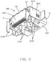
- FIG. 2 is another perspective view of the electrical connector of FIG. 1 ;
- FIG. 3 is an exploded perspective view of the electrical connector of FIG. 1 ;
- FIG. 4 is another exploded perspective view of the electrical connector of FIG. 3 ;
- FIG. 5 is an exploded perspective view of the contact module of the electrical connector of FIG. 1 ;
- FIG. 6 is another exploded perspective view of the contact module of the electrical connector of FIG. 5 ;
- FIG. 7 is a perspective view of the contacts of the contact module of the electrical connector of FIG. 5 ;
- FIG. 8 is another perspective view of the contacts of the contact module of the electrical connector of FIG. 7 ;
- FIG. 9 is a cross-sectional view of the electrical connector of FIG. 1 ;
- FIG. 10 is another cross-sectional view of the electrical connector of FIG. 1 .
- an HDMI electrical connector 100 for mounting to a printed circuit board (not shown) and mated with a plug connector (not shown), includes a contact module composed of an insulative housing 1 and a plurality of contacts 2 integrally formed within the housing 1 via a one shot injection molding process.
- the housing includes a base 11 and a mating tongue 12 forwardly extending from the base 11 .
- Each contact 2 has a front contacting section 23 exposed upon the mating tongue 12 , a mounting section 24 extending out of the base 11 , and a linking section 25 linked between the contacting section 23 and the mounting section 24 .
- the contacts 2 include a first row contacts 21 and the second row contacts 2 alternately arranged with each other along the transverse direction.
- the first row contacts 21 and the second row contacts 22 commonly form a first group 201 having a pair of differential pair signal contacts 26 of the first row contacts 21 and a grounding/shielding contact 27 of the second row contacts 22 .
- the pair of differential pair signal contacts 26 of the first row contacts 21 and the corresponding grounding contact 27 of the second row contacts 22 in the first group commonly form an isosceles triangle in a cross-sectional view wherein the grounding contact 27 is located at the center apex.
- the first group 201 is located at the outer most position of the contacts 2 .
- the outer differential pair signal contact 26 in the first group 201 has no neighboring contact on its outer side, thus affecting the corresponding impedance thereof compared with other (internal) groups having the neighboring contacts by two sides thereof. Therefore, the corresponding grounding contact 27 has some difference compared with the grounding contacts 27 of the other group.
- the linking section 25 of the grounding contact 27 of the first group 201 has a (wider) width of 0.35 mm while those of grounding contacts of other groups has a (narrower) width of 0.25 mm only. Understandably, such a difference is to compensate the impedance difference or lower the impedance thereof due to lacking the neighboring contact of the outer differential pair signal contact 26 of the first group 201 .
- the first row contacts 21 and the second row contacts 22 further include with the same pattern, i.e., the pair of differential pair signal contacts 26 being in one row while the grounding contact 27 in the other row, the second group 202 , the third group 203 and the fourth group 204 each of which forms the isosceles triangular cross-section with the corresponding grounding contact at the center apex, and such triangular configurations of the all the first group 201 , the second group 202 , the third group 203 and the fourth group 204 are essentially alternately arranged in a staggered mutually reversed manner, i.e., one upstanding type and one upside-down type alternately arranged with each other along the transverse direction.
- the mating interface complies with the HDMI specification wherein there are ten first row contacts 21 and nine second row contacts 22 wherein the first group 201 is located at the leftmost (outermost) side, requiring widening the linking section 25 of the corresponding grounding contact 27 .
- the first row contacts 21 there is another grounding contact 28 and a power contact 29 .
- the linking section 25 of the grounding contact 28 may have a width between that of the grounding contact 27 of the first group 201 and those of the remaining contacts 2 .
- the width of the linking section 25 of the grounding contact 27 of the first group 201 is 0.35 mm
- that of the grounding contact 28 is 0.3 mm
- those of the remaining contacts 2 are 0.25 mm.
- a front end 230 of the contacting section 23 is inwardly bent toward and embedded at the mid-level of the mating tongue 12 .
- the width of the front end 230 is smaller than that of the contacting section 23 .
- the connector 100 further includes a metallic shell 3 enclosing the housing 1 to form a mating cavity 4 around the mating tongue 12 .
- the shell 3 includes a main shell 31 and a sub-shell 32 attached to the main shell 31 .
- the main shell 31 includes an upper wall 311 , a lower wall 312 and two side walls 313 therebetween. Each side wall 313 has the corresponding mounting leg 3130 .
- the sub-shell 32 has the main part 321 covering the top wall 311 , and a rear part 322 extending downwardly from the rear edge of the main part 321 to cover the rear face of the base 11 .
- the base 11 further includes a positioning block 110 .
- the upper wall 311 forms a notch 3110 to receive the corresponding positioning block 110
- the sub-shell 32 forms an opening 323 corresponding to the corresponding positioning block 110 too so as to have the hosing 1 retained to the shell 3 .
- the base 11 includes a pair of supports 111 and the lower wall 312 is seated upon the support 111 , and the upper wall 311 is seated upon the upper face 112 of the base 11 so as to allow the main shell 31 to be assembled to the housing along the front-to-back direction.
- the sub-shell 32 has a plurality of side parts 3210 extending downwardly from the main part 321 to cover the side walls 313 .
- Each side part 3210 has the tab 3211 to be engaged within the corresponding recess 3131 in the corresponding side wall 313 so as to allow the sub-shell 32 to be upwardly assembled to the main shell 31 and assembled together.
- One feature of the invention is to increase the width of the connecting section 25 of the outermost grounding/shielding contact 27 in comparison with the remaining contacts 2 .
- Another feature of the invention is regarding the contacts 2 are all integrally formed with the housing 1 in a one shot insert-molding process.
- the front ends 230 of the contacting sections 23 of all contacts 2 are arranged in a first plane
- the linking sections 25 of all the contacts 2 are arranged in a second plane horizontal plane which is essentially coplanar with the first plane in this embodiment
- the mounting sections 24 of all the contacts 2 are arranged in a third plane lower than both the first plane and the second plane.
- the mating tongue 12 forms a plurality of upward blind holes (not labeled) and a plurality of downward blind holes (not labeled) alternately arranged with each other along the transverse direction where the core pins of the mold are positioned for forming the mating tongue 12 of the housing 1 during injection molding process, wherein each blind forms a trapezoidal cross-section with an larger opening facing toward the exterior in the vertical direction and a small opening covered by the corresponding contacting section 23 in the vertical direction.
- the housing forms a hole (not labeled) aligned with the linking section 25 of each contact 2 so as to implement the one shot injection molding without risk of tilting of the corresponding linking section 25 .
- each upward blind hole extends along the front-to-back direction with two supporting blocks (not labeled) which are transversely linked with those of the neighboring downward blind holes for reinforcement of the whole mating tongue 12 .
Landscapes
- Details Of Connecting Devices For Male And Female Coupling (AREA)
Abstract
Description
Claims (11)
Applications Claiming Priority (3)
| Application Number | Priority Date | Filing Date | Title |
|---|---|---|---|
| CN201821338757.1U CN208580906U (en) | 2018-08-17 | 2018-08-17 | HDMI electric connector |
| CN201821338757U | 2018-08-17 | ||
| CN201821338757.1 | 2018-08-17 |
Publications (2)
| Publication Number | Publication Date |
|---|---|
| US20200059044A1 US20200059044A1 (en) | 2020-02-20 |
| US10826246B2 true US10826246B2 (en) | 2020-11-03 |
Family
ID=65512407
Family Applications (1)
| Application Number | Title | Priority Date | Filing Date |
|---|---|---|---|
| US16/544,849 Active US10826246B2 (en) | 2018-08-17 | 2019-08-19 | Contact arrangement of electrical connector |
Country Status (3)
| Country | Link |
|---|---|
| US (1) | US10826246B2 (en) |
| CN (1) | CN208580906U (en) |
| TW (1) | TWM595347U (en) |
Cited By (1)
| Publication number | Priority date | Publication date | Assignee | Title |
|---|---|---|---|---|
| US12537351B2 (en) * | 2022-05-06 | 2026-01-27 | Jess-Link Products Co., Ltd. | Multimedia socket connector with fracture opening and manufacturing method thereof |
Families Citing this family (7)
| Publication number | Priority date | Publication date | Assignee | Title |
|---|---|---|---|---|
| CN112448235B (en) * | 2019-09-04 | 2022-05-31 | 上海莫仕连接器有限公司 | Electric connector and circuit board thereof |
| TWI729716B (en) * | 2020-02-27 | 2021-06-01 | 維將科技股份有限公司 | Electric connector (10) |
| US11322869B2 (en) * | 2020-05-19 | 2022-05-03 | TE Connectivity Services Gmbh | Electrical connector having a ground bus |
| TWI824244B (en) * | 2020-06-04 | 2023-12-01 | 貝爾威勒電子股份有限公司 | Electrical connector |
| CN115693307B (en) * | 2022-10-11 | 2025-08-01 | 东莞凯科电子科技有限公司 | HDMI interface structure with high signal transmission efficiency |
| JP2024064484A (en) * | 2022-10-28 | 2024-05-14 | ヒロセ電機株式会社 | Connector device that can be connected to the same type connector |
| TWI870866B (en) * | 2023-05-19 | 2025-01-21 | 富佳得實業股份有限公司 | Electrical connector |
Citations (8)
| Publication number | Priority date | Publication date | Assignee | Title |
|---|---|---|---|---|
| TWM419303U (en) | 2011-05-18 | 2011-12-21 | Hon Hai Prec Ind Co Ltd | Electrical connector |
| US8506332B2 (en) * | 2008-02-26 | 2013-08-13 | Molex Incorporated | Impedance controlled electrical connector |
| US9496651B2 (en) * | 2015-03-03 | 2016-11-15 | Lattice Semiconductor Corporation | HDMI connector |
| US20160352052A1 (en) * | 2015-05-29 | 2016-12-01 | Foxconn Interconnect Technology Limited | Electrcial connector with improved shielding performance |
| US20170018883A1 (en) * | 2015-07-16 | 2017-01-19 | Advanced-Connectek Inc. | Electrical receptacle connector |
| US20180006408A1 (en) * | 2016-06-30 | 2018-01-04 | Foxconn Interconnect Technology Limited | Electrical connector having improved conductive terminals |
| TWI612736B (en) | 2014-12-23 | 2018-01-21 | Advanced Connectek Inc | Anti-interference plug electrical connector |
| US9917391B2 (en) * | 2016-06-02 | 2018-03-13 | Foxconn Interconnect Technology Limited | Electrical connector having widened and added power terminals |
-
2018
- 2018-08-17 CN CN201821338757.1U patent/CN208580906U/en active Active
-
2019
- 2019-08-15 TW TW108210784U patent/TWM595347U/en unknown
- 2019-08-19 US US16/544,849 patent/US10826246B2/en active Active
Patent Citations (8)
| Publication number | Priority date | Publication date | Assignee | Title |
|---|---|---|---|---|
| US8506332B2 (en) * | 2008-02-26 | 2013-08-13 | Molex Incorporated | Impedance controlled electrical connector |
| TWM419303U (en) | 2011-05-18 | 2011-12-21 | Hon Hai Prec Ind Co Ltd | Electrical connector |
| TWI612736B (en) | 2014-12-23 | 2018-01-21 | Advanced Connectek Inc | Anti-interference plug electrical connector |
| US9496651B2 (en) * | 2015-03-03 | 2016-11-15 | Lattice Semiconductor Corporation | HDMI connector |
| US20160352052A1 (en) * | 2015-05-29 | 2016-12-01 | Foxconn Interconnect Technology Limited | Electrcial connector with improved shielding performance |
| US20170018883A1 (en) * | 2015-07-16 | 2017-01-19 | Advanced-Connectek Inc. | Electrical receptacle connector |
| US9917391B2 (en) * | 2016-06-02 | 2018-03-13 | Foxconn Interconnect Technology Limited | Electrical connector having widened and added power terminals |
| US20180006408A1 (en) * | 2016-06-30 | 2018-01-04 | Foxconn Interconnect Technology Limited | Electrical connector having improved conductive terminals |
Cited By (1)
| Publication number | Priority date | Publication date | Assignee | Title |
|---|---|---|---|---|
| US12537351B2 (en) * | 2022-05-06 | 2026-01-27 | Jess-Link Products Co., Ltd. | Multimedia socket connector with fracture opening and manufacturing method thereof |
Also Published As
| Publication number | Publication date |
|---|---|
| US20200059044A1 (en) | 2020-02-20 |
| CN208580906U (en) | 2019-03-05 |
| TWM595347U (en) | 2020-05-11 |
Similar Documents
| Publication | Publication Date | Title |
|---|---|---|
| US10826246B2 (en) | Contact arrangement of electrical connector | |
| US9276365B2 (en) | Electrical connector with grounding mechanism contacting outer shell | |
| US8894451B2 (en) | Differential signal connector capable of reducing skew between a differential signal pair | |
| US6843686B2 (en) | High-frequency electric connector having no ground terminals | |
| US9214766B1 (en) | Electrical connector having a metallic inner shell between a metallic outer shell and an insulative housing | |
| KR101292368B1 (en) | Multipolar connector | |
| US10069262B2 (en) | Receptacle connector having insert molded lead-frame wafers each with upper contacts transversely offset from lower contacts | |
| JP5756110B2 (en) | Plug-in connection including shielding | |
| US9306337B2 (en) | Electrical connector with inner shell in two pieces | |
| US10553966B1 (en) | Wire arrangement with ground staples on printed circuit board | |
| US20200412060A1 (en) | Electrical connector structure | |
| US7993161B2 (en) | Low profile connector with combo solder tails | |
| CN100539322C (en) | Board Mount Electrical Connectors | |
| US9099819B2 (en) | Electrical connector having shielding members | |
| TW201526403A (en) | Connector | |
| CN102292875A (en) | Impedance controlled electrical connector | |
| TW202310519A (en) | Connector | |
| CN105207012A (en) | Electrical connector having common ground shield | |
| KR20150031199A (en) | Electrical Connector | |
| CN101505025B (en) | Connector | |
| US8007294B2 (en) | Connector | |
| US20110045705A1 (en) | Elelctrical connector with improved terminals assembled to insulative housing from top to bottom | |
| US10720733B2 (en) | Electrical connector terminal assembly with terminals having a very specific profile | |
| CN115347419A (en) | Electric connector and electric connector combination | |
| US9306359B2 (en) | Well co-plane card edge connector |
Legal Events
| Date | Code | Title | Description |
|---|---|---|---|
| AS | Assignment |
Owner name: FOXCONN INTERCONNECT TECHNOLOGY LIMITED, CAYMAN ISLANDS Free format text: ASSIGNMENT OF ASSIGNORS INTEREST;ASSIGNORS:ZHANG, WEI-LIANG;HU, JIAN-LONG;WANG, XIANG-DONG;AND OTHERS;REEL/FRAME:050093/0947 Effective date: 20190805 Owner name: FU DING PRECISION INDUSTRIAL (ZHENGZHOU) CO.,LTD., CHINA Free format text: ASSIGNMENT OF ASSIGNORS INTEREST;ASSIGNORS:ZHANG, WEI-LIANG;HU, JIAN-LONG;WANG, XIANG-DONG;AND OTHERS;REEL/FRAME:050093/0947 Effective date: 20190805 |
|
| FEPP | Fee payment procedure |
Free format text: ENTITY STATUS SET TO UNDISCOUNTED (ORIGINAL EVENT CODE: BIG.); ENTITY STATUS OF PATENT OWNER: LARGE ENTITY |
|
| STPP | Information on status: patent application and granting procedure in general |
Free format text: DOCKETED NEW CASE - READY FOR EXAMINATION |
|
| STPP | Information on status: patent application and granting procedure in general |
Free format text: PUBLICATIONS -- ISSUE FEE PAYMENT VERIFIED |
|
| STCF | Information on status: patent grant |
Free format text: PATENTED CASE |
|
| MAFP | Maintenance fee payment |
Free format text: PAYMENT OF MAINTENANCE FEE, 4TH YEAR, LARGE ENTITY (ORIGINAL EVENT CODE: M1551); ENTITY STATUS OF PATENT OWNER: LARGE ENTITY Year of fee payment: 4 |