US10825827B2 - Non-volatile memory with pool capacitor - Google Patents
Non-volatile memory with pool capacitor Download PDFInfo
- Publication number
- US10825827B2 US10825827B2 US16/141,149 US201816141149A US10825827B2 US 10825827 B2 US10825827 B2 US 10825827B2 US 201816141149 A US201816141149 A US 201816141149A US 10825827 B2 US10825827 B2 US 10825827B2
- Authority
- US
- United States
- Prior art keywords
- pad
- memory array
- section
- conductive layers
- vertical columns
- Prior art date
- Legal status (The legal status is an assumption and is not a legal conclusion. Google has not performed a legal analysis and makes no representation as to the accuracy of the status listed.)
- Active
Links
Images


Classifications
-
- H01L27/11582—
-
- H—ELECTRICITY
- H10—SEMICONDUCTOR DEVICES; ELECTRIC SOLID-STATE DEVICES NOT OTHERWISE PROVIDED FOR
- H10B—ELECTRONIC MEMORY DEVICES
- H10B43/00—EEPROM devices comprising charge-trapping gate insulators
- H10B43/20—EEPROM devices comprising charge-trapping gate insulators characterised by three-dimensional [3D] arrangements, e.g. with cells on different height levels
- H10B43/23—EEPROM devices comprising charge-trapping gate insulators characterised by three-dimensional [3D] arrangements, e.g. with cells on different height levels with source and drain on different levels, e.g. with sloping channels
- H10B43/27—EEPROM devices comprising charge-trapping gate insulators characterised by three-dimensional [3D] arrangements, e.g. with cells on different height levels with source and drain on different levels, e.g. with sloping channels the channels comprising vertical portions, e.g. U-shaped channels
-
- G—PHYSICS
- G11—INFORMATION STORAGE
- G11C—STATIC STORES
- G11C16/00—Erasable programmable read-only memories
- G11C16/02—Erasable programmable read-only memories electrically programmable
- G11C16/04—Erasable programmable read-only memories electrically programmable using variable threshold transistors, e.g. FAMOS
- G11C16/0483—Erasable programmable read-only memories electrically programmable using variable threshold transistors, e.g. FAMOS comprising cells having several storage transistors connected in series
-
- G—PHYSICS
- G11—INFORMATION STORAGE
- G11C—STATIC STORES
- G11C16/00—Erasable programmable read-only memories
- G11C16/02—Erasable programmable read-only memories electrically programmable
- G11C16/06—Auxiliary circuits, e.g. for writing into memory
- G11C16/10—Programming or data input circuits
-
- G—PHYSICS
- G11—INFORMATION STORAGE
- G11C—STATIC STORES
- G11C16/00—Erasable programmable read-only memories
- G11C16/02—Erasable programmable read-only memories electrically programmable
- G11C16/06—Auxiliary circuits, e.g. for writing into memory
- G11C16/26—Sensing or reading circuits; Data output circuits
- G11C16/28—Sensing or reading circuits; Data output circuits using differential sensing or reference cells, e.g. dummy cells
-
- G—PHYSICS
- G11—INFORMATION STORAGE
- G11C—STATIC STORES
- G11C16/00—Erasable programmable read-only memories
- G11C16/02—Erasable programmable read-only memories electrically programmable
- G11C16/06—Auxiliary circuits, e.g. for writing into memory
- G11C16/32—Timing circuits
-
- G—PHYSICS
- G11—INFORMATION STORAGE
- G11C—STATIC STORES
- G11C5/00—Details of stores covered by group G11C11/00
- G11C5/14—Power supply arrangements, e.g. power down, chip selection or deselection, layout of wirings or power grids, or multiple supply levels
-
- G—PHYSICS
- G11—INFORMATION STORAGE
- G11C—STATIC STORES
- G11C7/00—Arrangements for writing information into, or reading information out from, a digital store
- G11C7/02—Arrangements for writing information into, or reading information out from, a digital store with means for avoiding parasitic signals
-
- G—PHYSICS
- G11—INFORMATION STORAGE
- G11C—STATIC STORES
- G11C7/00—Arrangements for writing information into, or reading information out from, a digital store
- G11C7/10—Input/output [I/O] data interface arrangements, e.g. I/O data control circuits, I/O data buffers
- G11C7/1048—Data bus control circuits, e.g. precharging, presetting, equalising
-
- G—PHYSICS
- G11—INFORMATION STORAGE
- G11C—STATIC STORES
- G11C7/00—Arrangements for writing information into, or reading information out from, a digital store
- G11C7/10—Input/output [I/O] data interface arrangements, e.g. I/O data control circuits, I/O data buffers
- G11C7/1051—Data output circuits, e.g. read-out amplifiers, data output buffers, data output registers, data output level conversion circuits
- G11C7/1057—Data output buffers, e.g. comprising level conversion circuits, circuits for adapting load
-
- G—PHYSICS
- G11—INFORMATION STORAGE
- G11C—STATIC STORES
- G11C7/00—Arrangements for writing information into, or reading information out from, a digital store
- G11C7/10—Input/output [I/O] data interface arrangements, e.g. I/O data control circuits, I/O data buffers
- G11C7/1078—Data input circuits, e.g. write amplifiers, data input buffers, data input registers, data input level conversion circuits
- G11C7/1084—Data input buffers, e.g. comprising level conversion circuits, circuits for adapting load
-
- G—PHYSICS
- G11—INFORMATION STORAGE
- G11C—STATIC STORES
- G11C7/00—Arrangements for writing information into, or reading information out from, a digital store
- G11C7/12—Bit line control circuits, e.g. drivers, boosters, pull-up circuits, pull-down circuits, precharging circuits, equalising circuits, for bit lines
-
- H01L27/1157—
-
- H01L27/11573—
-
- H—ELECTRICITY
- H10—SEMICONDUCTOR DEVICES; ELECTRIC SOLID-STATE DEVICES NOT OTHERWISE PROVIDED FOR
- H10B—ELECTRONIC MEMORY DEVICES
- H10B43/00—EEPROM devices comprising charge-trapping gate insulators
- H10B43/30—EEPROM devices comprising charge-trapping gate insulators characterised by the memory core region
- H10B43/35—EEPROM devices comprising charge-trapping gate insulators characterised by the memory core region with cell select transistors, e.g. NAND
-
- H—ELECTRICITY
- H10—SEMICONDUCTOR DEVICES; ELECTRIC SOLID-STATE DEVICES NOT OTHERWISE PROVIDED FOR
- H10B—ELECTRONIC MEMORY DEVICES
- H10B43/00—EEPROM devices comprising charge-trapping gate insulators
- H10B43/40—EEPROM devices comprising charge-trapping gate insulators characterised by the peripheral circuit region
-
- G—PHYSICS
- G11—INFORMATION STORAGE
- G11C—STATIC STORES
- G11C2207/00—Indexing scheme relating to arrangements for writing information into, or reading information out from, a digital store
- G11C2207/10—Aspects relating to interfaces of memory device to external buses
- G11C2207/105—Aspects related to pads, pins or terminals
-
- H—ELECTRICITY
- H10—SEMICONDUCTOR DEVICES; ELECTRIC SOLID-STATE DEVICES NOT OTHERWISE PROVIDED FOR
- H10B—ELECTRONIC MEMORY DEVICES
- H10B43/00—EEPROM devices comprising charge-trapping gate insulators
- H10B43/10—EEPROM devices comprising charge-trapping gate insulators characterised by the top-view layout
-
- H—ELECTRICITY
- H10—SEMICONDUCTOR DEVICES; ELECTRIC SOLID-STATE DEVICES NOT OTHERWISE PROVIDED FOR
- H10D—INORGANIC ELECTRIC SEMICONDUCTOR DEVICES
- H10D1/00—Resistors, capacitors or inductors
- H10D1/60—Capacitors
- H10D1/68—Capacitors having no potential barriers
- H10D1/692—Electrodes
- H10D1/711—Electrodes having non-planar surfaces, e.g. formed by texturisation
- H10D1/714—Electrodes having non-planar surfaces, e.g. formed by texturisation having horizontal extensions
Definitions
- Semiconductor memory is widely used in various electronic devices such as cellular telephones, digital cameras, personal digital assistants, medical electronics, mobile computing devices, servers, solid state drives, non-mobile computing devices and other devices.
- Semiconductor memory may comprise non-volatile memory or volatile memory.
- a non-volatile memory allows information to be stored and retained even when the non-volatile memory is not connected to a source of power (e.g., a battery).
- Examples of non-volatile memory include flash memory (e.g., NAND-type and NOR-type flash memory).
- Memory systems can be used to store data provided by a host device, client, user or other entity. It is important that the memory system function properly so that data can be stored in the memory system and read back accurately.
- FIG. 1 is a block diagram of one embodiment of a memory die.
- FIG. 2 is a perspective view of a portion of one embodiment of a monolithic three dimensional memory structure.
- FIG. 3A is a block diagram of a memory structure having two planes.
- FIG. 3B depicts a top view of a portion of a block of memory cells.
- FIG. 3C depicts a cross sectional view of a portion of a block of memory cells.
- FIG. 3D depicts a view of the select gate layers and word line layers.
- FIG. 3E is a cross sectional view of a vertical column of memory cells.
- FIG. 3F is a schematic of a plurality of NAND strings showing multiple sub-blocks.
- FIG. 4 is a block diagram of a memory die.
- FIG. 5 depicts the connection of word lines to I/O pads; for example, depict the word lines functioning as a capacitor connected to the power I/O pad.
- FIG. 6 is a top view of one embodiment of a three dimensional memory structure.
- FIG. 7 depicts layers in one embodiment of a three dimensional memory structure.
- FIG. 8 depicts two planes of one embodiment of a three dimensional memory structure and bit lines across the planes.
- FIG. 9 depicts layers in one embodiment of a three dimensional memory structure.
- FIG. 10 is a flow chart describing a portion of one embodiment of a process for fabricating a memory die.
- FIG. 11 is a flow chart describing a portion of one embodiment of a process for adding a three dimensional memory structure.
- FIG. 12 is a symbolic schematic diagram showing a pool capacitor connected to the I/O interface.
- FIG. 13 is a cross sectional view of a vertical column of memory cells.
- FIG. 14 depicts layers in one embodiment of a three dimensional memory structure.
- FIG. 15 depicts layers in one embodiment of a three dimensional memory structure.
- FIG. 16A depicts a top view of the selection line layer of the three dimensional memory structure functioning as a capacitor connected to the power I/O pad.
- FIG. 16B is a symbolic schematic diagram showing a pool capacitor connected to the power I/O pad.
- FIG. 17 depicts a top view of the selection line layer above the three dimensional memory structure functioning as a capacitor connected to the power I/O pad.
- FIG. 18 depicts layers in one embodiment of a three dimensional memory structure.
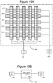
- FIG. 19A depicts a top view of layers above the three dimensional memory structure functioning as a capacitor connected to the power I/O pad.
- FIG. 19B is a symbolic schematic diagram showing a pool capacitor connected to the power I/O pad.
- FIG. 20A depicts a top view of layers above the three dimensional memory structure functioning as a capacitor connected to the power I/O pad.
- FIG. 20B is a symbolic schematic diagram showing a pool capacitor connected to the power I/O pad.
- FIG. 21 is a flow chart describing a portion of one embodiment of a process for fabricating a memory die.
- a memory die is a semiconductor die that has a memory system implemented thereon.
- a memory die has a memory structure, peripheral circuits connected to the memory structure and an Input/Output (“I/O”) interface connected to the peripheral circuits and the memory structure.
- I/O interface is a structure that serves as the point where signals inside the memory die meet signals outside the memory die.
- One embodiment of an I/O interface includes a set of I/O pads, which allow signals internal to the memory die to connect to the world outside of the memory die.
- the I/O pads are connected to I/O pins of a package.
- the set of I/O pads of the I/O interface includes data I/O pads for data signals, control I/O pads for control signals, power I/O pads for power, and ground I/O pads to connect to ground.
- One embodiment includes a non-volatile memory structure, a peripheral circuit connected to the memory structure, and an I/O interface connected to the peripheral circuit.
- a section (e.g., an unused section) of the memory structure is configured to operate as a capacitor and is connected to the I/O interface.
- Another embodiment includes a non-volatile memory structure comprising a user data section and a dummy section, a capacitor positioned above the dummy section and an I/O interface connected to the capacitor.
- FIG. 1 is a functional block diagram of one embodiment of a memory die 300 that implements the technology proposed herein for using a portion of memory die as a pool capacitor for the I/O interface.
- the components depicted in FIG. 1 are electrical circuits.
- each memory die 300 includes a memory structure 326 , control circuitry 310 , and read/write circuits 328 .
- Memory structure 326 is addressable by word lines via a row decoder 324 and by bit lines via a column decoder 332 .
- the read/write circuits 328 include multiple sense blocks 350 including SB 1 , SB 2 , . . .
- each sense block include a sense amplifier and a set of latches connected to the bit line.
- the latches store data to be written and/or data that has been read.
- the sense amplifiers include bit line drivers.
- Memory dies 300 includes I/O interface 321 , which is connected to control circuitry 310 , column decoder 332 , read/write circuits 328 and memory structure 326 . Commands and data are transferred between the controller and the memory die 300 via lines 319 that connect to I/O interface 321 .
- I/O interface 321 includes a set of I/O pads.
- I/O interface 321 can be a synchronous interface or an asynchronous interface. Examples of an I/O interface include a Toggle Mode Interface and an Open NAD Flash Interface (ONFI). Other I/O interfaces can also be used.
- Toggle mode e.g., Toggle Mode 2.0 JEDEC Standard or Toggle Mode 800
- Table 1 provides a definition of one example of a Toggle Mode Interface. For each of the signals listed in the table below, I/O Interface has a corresponding I/O pad.
- ALE Input Address Latch Enable controls the activating path for addresses to the internal address registers. Addresses are latched on the rising edge of WEn with ALE high.
- CEn Chip Enable controls memory die selection.
- CLE Input Command Latch Enable controls the activating path for commands sent to the command register. When active high, commands are latched into the command register through the I/O ports on the rising edge of the WEn signal.
- RE Input Read Enable Complement REn Input Read Enable controls serial data out, and when active, drives the data onto the I/O bus.
- WEn Input Write Enable controls writes to the I/O port. Commands and addresses are latched on the rising edge of the WEn pulse.
- WPn Input Write Protect provides inadvertent program/erase protection during power transitions.
- the internal high voltage generator is reset when the WPn pin is active low.
- DQS Input/Output Data Strobe acts as an output when reading data, and as an input when writing data.
- DQS is edge-aligned with data read; it is center- aligned with data written.
- DQSn Input/Output Data Strobe complement (used for DDR) Bus[0:7] Input/Output Data Input/Output (I/O) bus inputs commands, addresses, and data, and outputs data during Read operations.
- the I/O pins float to High-z when the chip is deselected or when outputs are disabled.
- R/Bn Output Ready/Busy indicates device operation status.
- R/Bn is an open-drain output and does not float to High-z when the chip is deselected or when outputs are disabled. When low, it indicates that a program, erase, or random read operation is in process; it goes high upon completion.
- VCCQ Supply I/O power for I/O signals VPP Supply Optional, high voltage, external power supply VREF Supply Reference voltage, reserved fir Toggle Mode DDR2 VSS Supply Ground
- control circuitry 310 cooperates with the read/write circuits 328 to perform memory operations (e.g., write, read, erase, and others) on memory structure 326 .
- control circuitry 310 includes a state machine 312 , an on-chip address decoder 314 , a power control circuit 316 and a temperature sensor circuit 318 .
- State machine 312 provides die-level control of memory operations.
- state machine 312 is programmable by software. In other embodiments, state machine 312 does not use software and is completely implemented in hardware (e.g., electrical circuits).
- state machine 312 can be replaced by a microcontroller or microprocessor.
- control circuitry 310 includes buffers such as registers, ROM fuses and other storage devices for storing default values such as base voltages and other parameters. Temperature sensor circuit 318 detects current temperature at memory die 300 .
- the on-chip address decoder 314 provides an address interface between addresses used by controller 120 to the hardware address used by the decoders 324 and 332 .
- Power control module 316 controls the power and voltages supplied to the word lines and bit lines during memory operations. Power control module 316 may include charge pumps for creating voltages.
- control circuitry 310 read/write circuits 328 and decoders 324 / 332 comprise one embodiment of a control circuit for memory structure 326 .
- other circuits that support and operate on memory structure 326 can be referred to as a control circuit.
- the controller can operate as the control circuit or can be part of the control circuit.
- memory structure 326 comprises a three dimensional memory array of non-volatile memory cells in which multiple memory levels are formed above a single substrate, such as a wafer.
- the memory structure may comprise any type of non-volatile memory that is monolithically formed in one or more physical levels of arrays of memory cells having an active area disposed above a silicon (or other type of) substrate.
- the non-volatile memory cells of memory structure 326 comprise vertical NAND strings with charge-trapping material such as described, for example, in U.S. Pat. No. 9,721,662, incorporated herein by reference in its entirety.
- a NAND string includes memory cells connected by a channel.
- memory structure 326 comprises a two dimensional memory array of non-volatile memory cells.
- the non-volatile memory cells are NAND flash memory cells utilizing floating gates such as described, for example, in U.S. Pat. No. 9,082,502, incorporated herein by reference in its entirety.
- Other types of memory cells e.g., NOR-type flash memory can also be used.
- memory structure 326 The exact type of memory array architecture or memory cell included in memory structure 326 is not limited to the examples above. Many different types of memory array architectures or memory cell technologies can be used to form memory structure 326 . No particular non-volatile memory technology is required for purposes of the new claimed embodiments proposed herein.
- Other examples of suitable technologies for memory cells of the memory structure 326 include ReRAM memories, magnetoresistive memory (e.g., MRAM, Spin Transfer Torque MRAM, Spin Orbit Torque MRAM), phase change memory (e.g., PCM), and the like.
- suitable technologies for architectures of memory structure 326 include two dimensional arrays, three dimensional arrays, cross-point arrays, stacked two dimensional arrays, vertical bit line arrays, and the like.
- cross point memory includes reversible resistance-switching elements arranged in cross point arrays accessed by X lines and Y lines (e.g., word lines and bit lines).
- the memory cells may include conductive bridge memory elements.
- a conductive bridge memory element may also be referred to as a programmable metallization cell.
- a conductive bridge memory element may be used as a state change element based on the physical relocation of ions within a solid electrolyte.
- a conductive bridge memory element may include two solid metal electrodes, one relatively inert (e.g., tungsten) and the other electrochemically active (e.g., silver or copper), with a thin film of the solid electrolyte between the two electrodes.
- the conductive bridge memory element may have a wide range of programming thresholds over temperature.
- Magnetoresistive memory stores data by magnetic storage elements.
- the elements are formed from two ferromagnetic plates, each of which can hold a magnetization, separated by a thin insulating layer.
- One of the two plates is a permanent magnet set to a particular polarity; the other plate's magnetization can be changed to match that of an external field to store memory.
- a memory device is built from a grid of such memory cells. In one embodiment for programming, each memory cell lies between a pair of write lines arranged at right angles to each other, parallel to the cell, one above and one below the cell. When current is passed through them, an induced magnetic field is created.
- Phase change memory exploits the unique behavior of chalcogenide glass.
- One embodiment uses a GeTe—Sb2Te3 super lattice to achieve non-thermal phase changes by simply changing the co-ordination state of the Germanium atoms with a laser pulse (or light pulse from another source). Therefore, the doses of programming are laser pulses.
- the memory cells can be inhibited by blocking the memory cells from receiving the light. Note that the use of “pulse” in this document does not require a square pulse, but includes a (continuous or non-continuous) vibration or burst of sound, current, voltage light, or other wave.
- FIG. 2 is a perspective view of a portion of one example embodiment of a monolithic three dimensional memory array that can comprise memory structure 326 , which includes a plurality non-volatile memory cells.
- FIG. 2 shows a portion of one block of memory.
- the structure depicted includes a set of bit lines BL positioned above a stack of alternating dielectric layers and conductive layers with vertical columns of materials extending through the dielectric layers and conductive layers.
- D one of the dielectric layers
- one of the conductive layers also called word line layers
- W The number of alternating dielectric layers and conductive layers can vary based on specific implementation requirements.
- One set of embodiments includes between 108-300 alternating dielectric layers and conductive layers.
- One example embodiment includes 96 data word line layers, 8 select layers, 6 dummy word line layers and 110 dielectric layers. More or less than 108-300 layers can also be used.
- the alternating dielectric layers and conductive layers are divided into four “fingers” or sub-blocks by local interconnects LI.
- FIG. 2 shows two fingers and two local interconnects LI.
- Source line layer SL below the alternating dielectric layers and word line layers is a source line layer SL.
- Vertical columns of materials also known as memory holes
- MH one of the vertical columns/memory holes
- NAND strings are formed by filling the vertical column/memory hole with materials including a charge-trapping material to create a vertical column of memory cells. Each memory cell can store one or more bits of data. More details of the three dimensional monolithic memory array that comprises memory structure 126 is provided below with respect to FIG. 3A-3F .
- FIG. 3A is a block diagram explaining one example organization of memory structure 326 , which is divided into two planes 302 and 304 . Each plane is then divided into M blocks. In one example, each plane has about 2000 blocks. However, different numbers of blocks and planes can also be used.
- a block of memory cells is a unit of erase. That is, all memory cells of a block are erased together. In other embodiments, memory cells can be grouped into blocks for other reasons, such as to organize the memory structure 326 to enable the signaling and selection circuits.
- a block represents a groups of connected memory cells as the memory cells of a block share a common set of unbroken word lines and unbroken bit lines.
- Block 0 and Block M ⁇ 1 of both planes 302 and 304 are at the edge of the memory structure (or otherwise referred to as being located in an edge region/section of the memory structure).
- FIGS. 3B-3F depict an example three dimensional (“3D”) NAND structure that corresponds to the structure of FIG. 2 and can be used to implement memory structure 326 of FIG. 1 .
- FIG. 3B is a block diagram depicting a top view of a portion of one block from memory structure 326 . The portion of the block depicted in FIG. 3B corresponds to portion 306 in block 2 of FIG. 3A . As can be seen from FIG. 3B , the block depicted in FIG. 3B extends in the direction of 332 . In one embodiment, the memory array has many layers; however, FIG. 3B only shows the top layer.
- FIG. 3B depicts a plurality of circles that represent the vertical columns.
- Each of the vertical columns include multiple select transistors (also referred to as a select gate or selection gate) and multiple memory cells.
- each vertical column implements a NAND string.
- FIG. 3B depicts vertical columns 422 , 432 , 442 and 452 .
- Vertical column 422 implements NAND string 482 .
- Vertical column 432 implements NAND string 484 .
- Vertical column 442 implements NAND string 486 .
- Vertical column 452 implements NAND string 488 . More details of the vertical columns are provided below. Since the block depicted in FIG. 3B extends in the direction of arrow 330 and in the direction of arrow 332 , the block includes more vertical columns than depicted in FIG. 3B
- FIG. 3B also depicts a set of bit lines 415 , including bit lines 411 , 412 , 413 , 414 , . . . 419 .
- FIG. 3B shows twenty four bit lines because only a portion of the block is depicted. It is contemplated that more than twenty four bit lines connected to vertical columns of the block. Each of the circles representing vertical columns has an “x” to indicate its connection to one bit line.
- bit line 414 is connected to vertical columns 422 , 432 , 442 and 452 .
- bit lines are positioned over the memory structure 325 and run along the entire length of the plane (e.g., from the top of plane 302 to the bottom of plane 302 ).
- the block depicted in FIG. 3B includes a set of local interconnects 402 , 404 , 406 , 408 and 410 that connect the various layers to a source line below the vertical columns.
- Local interconnects 402 , 404 , 406 , 408 and 410 also serve to divide each layer of the block into four regions; for example, the top layer depicted in FIG. 3B is divided into regions 420 , 430 , 440 and 450 , which are referred to as fingers or sub-blocks.
- the four regions are referred to as word line fingers that are separated by the local interconnects.
- the word line fingers on a common level of a block connect together to form a single word line.
- the word line fingers on the same level are not connected together.
- a bit line only connects to one vertical column in each of regions 420 , 430 , 440 and 450 .
- each block has sixteen rows of active columns and each bit line connects to four rows in each block.
- all of four rows connected to a common bit line are connected to the same word line (via different word line fingers on the same level that are connected together); therefore, the system uses the source side selection lines and the drain side selection lines to choose one (or another subset) of the four to be subjected to a memory operation (program, verify, read, and/or erase).
- FIG. 3B shows each region having four rows of vertical columns, four regions and sixteen rows of vertical columns in a block, those exact numbers are an example implementation. Other embodiments may include more or less regions per block, more or less rows of vertical columns per region and more or less rows of vertical columns per block.
- FIG. 3B also shows the vertical columns being staggered. In other embodiments, different patterns of staggering can be used. In some embodiments, the vertical columns are not staggered.
- FIG. 3C depicts a portion of one embodiment of a three dimensional memory structure 326 showing a cross-sectional view along line AA of FIG. 3B .
- This cross sectional view cuts through vertical columns 432 and 434 and region 430 (see FIG. 3B ).
- the structure of FIG. 3C includes four drain side select layers SGD 0 , SGD 1 , SGD 2 and SGD 3 ; four source side select layers SGS 0 , SGS 1 , SGS 2 and SGS 3 ; six dummy word line layers DD 0 , DD 1 , DS 0 , DS 1 , WLDL, WLDU; and ninety six data word line layers WLL 0 -WLL 95 for connecting to data memory cells.
- each vertical column comprises a vertical NAND string.
- vertical column 432 comprises NAND string 484 .
- substrate 101 an insulating film 454 on the substrate, and source line SL.
- the NAND string of vertical column 432 has a source end at a bottom of the stack and a drain end at a top of the stack.
- FIG. 3C show vertical column 432 connected to Bit Line 414 via connector 415 .
- Local interconnects 404 and 406 are also depicted.
- drain side select layers SGD 0 , SGD 1 , SGD 2 and SGD 3 ; source side select layers SGS 0 , SGS 1 , SGS 2 and SGS 3 ; dummy word line layers DD 0 , DD 1 , DS 0 , DS 1 , WLDL and WLDU; and word line layers WLL 0 -WLL 95 collectively are referred to as the conductive layers.
- the conductive layers are made from a combination of TiN and Tungsten.
- other materials can be used to form the conductive layers, such as doped polysilicon, metal such as Tungsten or metal silicide.
- different conductive layers can be formed from different materials.
- dielectric layers DL 0 -DL 111 Between conductive layers are dielectric layers DL 0 -DL 111 .
- dielectric layers DL 104 is above word line layer WLL 94 and below word line layer WLL 95 .
- the dielectric layers are made from SiO 2 . In other embodiments, other dielectric materials can be used to form the dielectric layers.
- the non-volatile memory cells are formed along vertical columns which extend through alternating conductive and dielectric layers in the stack.
- the memory cells are arranged in NAND strings.
- the word line layers WLL 0 -WLL 95 connect to memory cells (also called data memory cells).
- Dummy word line layers DD 0 , DD 1 , DS 0 , DS 1 , WLDL and WLDU connect to dummy memory cells.
- a dummy memory cell does not store and is not eligible to store host data (data provided from the host, such as data from a user of the host), while a data memory cell is eligible to store host data.
- data memory cells and dummy memory cells may have a same structure.
- Drain side select layers SGD 0 , SGD 1 , SGD 2 and SGD 3 are used to electrically connect and disconnect NAND strings from bit lines.
- Source side select layers SGS 0 , SGS 1 , SGS 2 and SGS 3 are used to electrically connect and disconnect NAND strings from the source line SL.
- FIG. 3C also shows a Joint area.
- one embodiment includes laying down a first stack of forty eight word line layers alternating with dielectric layers, laying down the Joint area, and laying down a second stack of forty eight word line layers alternating with dielectric layers.
- the Joint area is positioned between the first stack and the second stack.
- the Joint area is used to connect to the first stack to the second stack.
- the first stack is labeled as the “Lower Set of Word Lines” and the second stack is labeled as the “Upper Set of Word Lines.”
- the Joint area is made from the same materials as the word line layers.
- the plurality of word lines comprises a first stack of alternating word line layers and dielectric layers, a second stack of alternating word line layers and dielectric layers, and a joint area between the first stack and the second stack, as depicted in FIG. 3C .
- FIG. 3D depicts a logical representation of the conductive layers (SGD 0 , SGD 1 , SGD 2 , SGD 3 , SGS 0 , SGS 1 , SGS 2 , SGS 3 , DD 0 , DD 1 , DS 0 , DS 1 , and WLL 0 -WLL 95 ) for the block that is partially depicted in FIG. 3C .
- local interconnects 402 , 404 , 406 , 408 and 410 break up the conductive layers into four regions/fingers (or sub-blocks).
- word line layer WLL 94 is divided into regions 460 , 462 , 464 and 466 .
- the regions are referred to as word line fingers; for example, word line layer WLL 126 is divided into word line fingers 460 , 462 , 464 and 466 .
- region 460 is one word line finger on one word line layer.
- the four word line fingers on a same level are connected together.
- each word line finger operates as a separate word line.
- Drain side select gate layer SGD 0 (the top layer) is also divided into regions 420 , 430 , 440 and 450 , also known as fingers or select line fingers.
- the four select line fingers on a same level are connected together.
- each select line finger operates as a separate word line.
- FIG. 3E depicts a cross sectional view of region 429 of FIG. 3C that includes a portion of vertical column 432 (a memory hole) that extends through the alternating conductive layers and dielectric layers.
- the vertical columns are round; however, in other embodiments other shapes can be used.
- vertical column 432 includes an inner core layer 470 that is made of a dielectric, such as SiO 2 . Other materials can also be used.
- Surrounding inner core 470 is polysilicon channel 471 . Materials other than polysilicon can also be used. Note that it is the channel 471 that connects to the bit line and the source line.
- Surrounding channel 471 is a tunneling dielectric 472 .
- tunneling dielectric 472 has an ONO structure.
- Surrounding tunneling dielectric 472 is charge trapping layer 473 , such as (for example) Silicon Nitride. Other memory materials and structures can also be used. The technology described herein is not limited to any particular material or structure.
- FIG. 3E depicts dielectric layers DLL 105 , DLL 104 , DLL 103 , DLL 102 and DLL 101 , as well as word line layers WLL 95 , WLL 94 , WLL 93 , WLL 92 , and WLL 91 .
- Each of the word line layers includes a word line region 476 surrounded by an aluminum oxide layer 477 , which is surrounded by a blocking oxide (SiO 2 ) layer 478 .
- the physical interaction of the word line layers with the vertical column forms the memory cells.
- a memory cell in one embodiment, comprises channel 471 , tunneling dielectric 472 , charge trapping layer 473 , blocking oxide layer 478 , aluminum oxide layer 477 and word line region 476 .
- word line layer WLL 95 and a portion of vertical column 432 comprise a memory cell MC 1 .
- Word line layer WLL 94 and a portion of vertical column 432 comprise a memory cell MC 2 .
- Word line layer WLL 93 and a portion of vertical column 432 comprise a memory cell MC 3 .
- Word line layer WLL 92 and a portion of vertical column 432 comprise a memory cell MC 4 .
- Word line layer WLL 91 and a portion of vertical column 432 comprise a memory cell MC 5 .
- a memory cell may have a different structure; however, the memory cell would still be the storage unit.
- a memory cell When a memory cell is programmed, electrons are stored in a portion of the charge trapping layer 473 which is associated with the memory cell. These electrons are drawn into the charge trapping layer 473 from the channel 471 , through the tunneling dielectric 472 , in response to an appropriate voltage on word line region 476 .
- the threshold voltage (Vth) of a memory cell is increased in proportion to the amount of stored charge.
- the programming is achieved through Fowler-Nordheim tunneling of the electrons into the charge trapping layer.
- the electrons return to the channel or holes are injected into the charge trapping layer to recombine with electrons.
- erasing is achieved using hole injection into the charge trapping layer via a physical mechanism such as gate induced drain leakage (GIDL).
- GIDL gate induced drain leakage
- FIG. 3F is a schematic diagram of a portion of the memory depicted in in FIGS. 2-3E .
- FIG. 3F shows physical word lines WLL 0 -WLL 95 running across the entire block.
- the structure of FIG. 3F corresponds to portion 306 in Block 2 of FIGS. 3A-E , including bit lines 411 , 412 , 413 , 414 , . . . 419 .
- each bit line is connected to four NAND strings. Drain side selection lines SGD 0 , SGD 1 , SGD 2 and SGD 3 are used to determine which of the four NAND strings connect to the associated bit line(s).
- Source side selection lines SGS 0 , SGS 1 , SGS 2 and SGS 3 are used to determine which of the four NAND strings connect to the common source line.
- the block can also be thought of as divided into four sub-blocks SB 0 , SB 1 , SB 2 and SB 3 .
- Sub-block SB 0 corresponds to those vertical NAND strings controlled by SGD 0 and SGS 0
- sub-block SB 1 corresponds to those vertical NAND strings controlled by SGD 1 and SGS 1
- sub-block SB 2 corresponds to those vertical NAND strings controlled by SGD 2 and SGS 2
- sub-block SB 3 corresponds to those vertical NAND strings controlled by SGD 3 and SGS 3 .
- FIG. 4 is a block diagram of a memory dies 502 that has converted unused portions of the memory die to usable pool capacitors for the power I/O pad.
- Memory die 502 may be the same structure as memory die 300 of FIG. 1 .
- Memory die 502 includes a three dimensional memory structure that includes two planes: Plane 0 ( 504 ) and Plane 1 ( 506 ).
- Plane 0 ( 504 ) may be the same structure as plane 302 of FIG. 3A .
- Plane 1 ( 506 ) may be the same structure as plane 304 of FIG. 3A . In other embodiments, more or less than two planes can be used.
- Plane 0 ( 504 ) and Plane 1 ( 506 ) may implement memory structure 325 , including any of the embodiments mentioned above.
- Memory die 502 also includes peripheral circuit 508 , which can be located to the side of the memory structure (Plane 0 and Plane 1 ) and/or underneath the memory structure (Plane 0 and Plane 1 ).
- Peripheral circuit 508 can include control circuitry 310 , read/write circuits 328 and decoders 324 / 332 .
- Peripheral circuit 508 can include any other circuit on the memory die that is used to control/operate the memory die.
- Memory die 508 also includes I/O Interface 510 , which may be the same as I/O Interface 321 of FIG. 1 .
- I/O Interface 510 may implement a Toggle Mode interface, as discussed above with respect to Table 1.
- Each I/O signal will include an I/O pad.
- I/O Interface 510 includes a power I/O pad (e.g., VCCQ) and a ground I/O pad (e.g., VSS).
- Block 504 a of Plane 0 is an edge block, as it is located at an edge section/region of the Plane 0 .
- Block 506 a of Plane 1 is an edge block, as it is located at an edge section/region of the Plane 1 .
- the edge blocks 504 a and 506 a are dummy blocks as they are not used to store user data (e.g., data provided from an entity outside of the memory die).
- the blocks that are in the interior or middle regions of Plane 0 and Plane 1 are user data blocks as they are used to store user data.
- Plane 0 includes an edge/dummy block at the other end of Plane 0 (opposite end from block 504 a ) and Plane 1 includes an edge/dummy block at the other end of Plane 1 (opposite end from block 506 a ).
- FIG. 1 shows one example embodiment of a non-volatile memory structure (Plane 0 and Plane 1 ), a peripheral circuit 504 connected to the memory structure, and an I/O interface 510 connected to the peripheral circuit 508 , where a section ( 504 a and/or 506 a ) of the memory structure is configured to operate as a capacitor and is connected to the I/O interface 510 .
- a section of the memory structure that includes multiple vertical columns has a first set of the conductive layers connected to the power I/O pad and a second set of the conductive layers connected to ground I/O pad such that the section of the memory structure functions as a capacitor connected to the power I/O pad, the first set of the conductive layers are interleaved with the second set of the conductive layers.
- the system of FIG. 4 can also position the capacitor above the unused dummy blocks 504 a and 506 a .
- a capacitor can be positioned above the dummy section with the I/O interface connected to the capacitor.
- the dummy blocks at the edge of the memory structure are configured to operate as a capacitor for the power I/O pad.
- the word lines of the dummy blocks 504 a and 506 a can be configured to operate as capacitors for any of the pad of I/O interface 510 , as depicted in FIG. 5 .
- alternating word lines are connected together.
- even numbered word lines can be connected together and odd numbered word lines can be connected together so that an even numbered word line and its neighboring odd numbered word line form a capacitor.
- Other arrangements of connecting word lines together can also be used.
- FIG. 5 shows all of the odd word lines (WL 1 , WL 3 , WL 5 , . . . WL 95 ) connected together. At one end of the word lines, all of the odd word lines are connected to switch 532 . Switch 532 is also connected to VSS pad 530 . At the other end of the word lines, all of the odd word lines are connected to switch 534 . Switch 534 is also connected to VSS pad 530 . Switches 532 and 534 are controlled by state machine 312 . When enabled, switches 532 and 534 connect the odd word lines to VSS pad 530 .
- FIG. 5 shows all of the even word lines (WL 0 , WL 2 , WL 4 , . . . WL 94 ) connected together. At one end of the word lines, all of the even word lines are connected to switch 542 . Switch 532 is also connected to VCCQ pad 540 . At the other end of the word lines, all of the even word lines are connected to switch 544 . Switch 544 is also connected to VCCQ pad 540 . Switches 542 and 544 are controlled by state machine 312 . When enabled, switches 542 and 544 connect the even word lines to VCCQ pad 540 .
- switches 532 and 542 are used (switches 534 and 544 are not used). In another embodiment, more than two switches are used per group of connected word lines. In one embodiment, switches 532 , 534 , 542 , and 544 are transistors.
- the even and odd word lines function/operate as a large pool capacitor that is connected to the VCCQ pad 540 . That is, the system is taking advantage of the capacitance between alternating word line layers. This large capacitance connected to VCCQ pad 540 stabilizes the current at the VCCQ pad and avoids the problem mentioned above with respect to DQS.
- the block (or other portion) of the memory structure being used has a first set of the conductive layers (e.g., word lines) connected to the power I/O pad and a second set of the conductive layers (e.g., word lines) connected to ground I/O pad such that the section of the memory structure functions as a capacitor connected to the power I/O pad.
- first set of the conductive layers e.g., word lines
- second set of the conductive layers e.g., word lines
- one embodiment in order to configure the dummy or edge block to function as capacitors, one embodiment includes adding switches to the block.
- configuring the dummy block (or edge block) to work as a capacitor also includes increasing the “highway width” to lower resistance of the word lines.
- the highway width refers to a gap between the vertical columns in a block and the adjacent border of the block or sub-block.
- FIG. 6 shows portions of two blocks: block 550 and block 552 .
- Block 550 is a user data block in the interior or middle section of the memory structure.
- Block 552 is a dummy block located at the edge of the memory structure.
- Block 550 includes local interconnects 560 for separating the block into four fingers or sub-blocks. In between the local interconnects 560 and the vertical columns (vc) are gaps 560 . These gaps 560 are the “highway width.”
- dummy/edge block 552 includes local interconnects 554 for separating the block into four fingers or sub-blocks. Within each finger or sub-block are a set of vertical columns (vc). Between the vertical columns and the local interconnects 554 are gaps 570 , also referred to as the highway width. In one embodiment, since the dummy/edge block 552 will be used as a pool capacitor for the VCCQ pad, the highway width or gap 570 for the dummy/edge block 552 is made wider than the highway width or gap 560 for the user data block in the interior of the memory structure. Another way to describe the highway width or gap 570 is a gap between the vertical columns (vc) and the adjacent border (e.g.
- the local interconnect 554 at the edge of the memory structure or at the edge of a sub-block of a memory structure.
- FIG. 7 depicts various layers of one embodiment of three-dimensional memory structure 326 in accordance with the embodiments of FIGS. 4-6 .
- FIG. 7 shows an active area AA which corresponds to the semiconductor substrate. Electrical circuits can be implemented on the active area.
- FIG. 7 shows three columns positioned on top of the active region: columns 602 , 604 and 606 .
- Column 602 pertains to peripheral circuit 508 (see FIG. 4 ).
- Column 604 pertains to a user data block in the interior of the memory structure.
- Column 606 pertains to a dummy block at the edge of the memory structure.
- Column 602 includes a first layer labeled as CS on top of the active area AA.
- This region CS is a connecting hole from the active area to the lowest metal layer MX; thereby, connecting circuits on the surface of the semiconductor substrate to the upper metal regions.
- the memory structure includes three metal layers: MX, M 0 , and M 1 . Connecting metal layer MX and M 0 is via V 0 . Connecting metal layer M 1 and M 0 is via V 1 .
- Each of the metal layers can initially be added to the device as a sheet and then patterned using standard processes known in the art.
- the bit lines are implemented in metal layer M 1 .
- Column 604 includes a vertical column vc (e.g. vertical NAND string) on top of active area AA.
- a vertical column vc e.g. vertical NAND string
- metal layer M 1 which serves as the bit line.
- Connecting the vertical column to the bit line in metal layer M 1 is a connecting hole CH (e.g. which is similar to a via) and via V 1 .
- the bit lines extend over all the blocks. Therefore, the bit lines extend over the dummy block at the edge of the memory structure; however, the bit lines are not connected to the vertical columns in the dummy block at the edge of the memory structure (in one embodiment).
- FIG. 7 shows column 606 including a vertical column vc on top of active area AA; however, the top of vertical column vc is not connected to metal layer M 1 (ie not connected to the bit line).
- metal layer M 1 ie not connected to the bit line.
- One reason for not connecting the bit line to the vertical columns of the dummy block is so that the vertical columns will be floating. Additionally, the SGS transistors are turned off to keep the vertical columns floating.
- FIG. 8 shows a three dimensional memory structure (e.g., memory structure 326 ) including Plane 0 ( 650 ) and Plane 1 ( 652 ). Each of the two planes have M blocks.
- Plane 0 ( 650 ) includes bit lines 660 which extend over all of the blocks except block 0 , where block 0 is the dummy block at the edge of the memory structure.
- Plane 2 ( 652 ) includes bit lines 662 that extend over all the blocks except block 0 , where block 0 is the dummy block at the edge of the memory structure.
- the memory system in addition to using capacitance between alternate word line layers, will additionally use capacitance between the word line layers and the vertical columns.
- Such an embodiment includes all the structural changes discussed above with respect to FIGS. 4-8 and one or more additional changes.
- the vertical columns (the vertical NAND strings) are connected to ground so that they form capacitors with those word lines connected to VCCQ.
- One means for connecting the vertical columns to ground is to turn on all of the SGS transistors (SGS 0 , SGS 1 , SGS 2 , SGS 3 —See FIG. 3 f ) and connect the source line SL ( FIG. 3F ) to ground.
- the SGS transistors can be turned on by applying a positive voltage (e.g., ⁇ 2.5-5v) to the gates via the selection lines.
- a positive voltage e.g., ⁇ 2.5-5v
- the source line can be at a DC ground (which is not necessarily AC ground).
- One example implementation also includes the bit lines not extending over the dummy block at the edge of the memory structure, as depicted in FIG. 8 , so as to avoid interference.
- FIG. 9 depicts the layers in one embodiment for a three-dimensional memory structure (e.g., memory structure 326 ).
- FIG. 9 shows the active area AA, representing the semiconductor substrate.
- Three columns are depicted: 680 , 682 and 684 .
- Column 682 and 684 depict portions of the dummy block at the edge of the memory structure.
- the bottom of column 682 and 684 represent the vertical columns vc (e.g. vertical NAND strings).
- connection holes ch which connect the vertical columns VC to metal layer M 0 .
- Metal layer M 0 is also connected to a Connection Hole CS of column 680 in order to connect down to a ground connection on the active area AA.
- FIG. 9 shows one connection hole CS connecting AA to M 0 , in other embodiments, there can be other intervening metal layers and vias. The arrangement of FIG. 9 allows the channels of vertical NAND strings of the vertical columns vc to be connected to ground through metal layer M 0 and another column 680 .
- FIG. 10 is a flowchart describing a portion of one embodiment of a process for fabricating a memory die according to the embodiments discussed above that include using alternate word line layers to provide extra capacitance to the power I/O pad (e.g. VCCQ).
- a three dimensional memory structure is added to the memory die, including fabricating an edge region (e.g., dummy block at edge of memory structure) of the memory structure different than a middle region (e.g., user data block away from the edge) of the memory structure.
- the edge region and the middle region also known as an interior region both include alternating conductive layers and dielectric layers with vertical columns of material extending through the conductive layers and the dielectric layers (as described above with respect to FIGS.
- a power I/O pad is added to the I/O interface.
- ground I/O pad is added to the I/O interface.
- Other pads can also be added to the I/O interface.
- a first set of the conductive layers in the edge region are connected to the power I/O pad and a second set of conductor layers in the edge region are connected to the ground I/O pad so that the edge region is configured to function as a pool capacitor for the power I/O pad.
- FIG. 11 is a flowchart describing a portion of one embodiment of a process that is performed as part of step 702 (in some embodiments).
- step 740 the middle region of the three-dimensional memory structure that was added in step 702 is connected to the bit lines.
- step 742 the edge region of the three-dimensional memory structure is electrically isolated from the bit lines.
- FIG. 7 shows no connection between the vertical column VC and the metal layer M 1 for column 606 .
- the bit lines can be patterned to not extend over the edge region.
- Step 744 includes creating first spaces in the edge region between the vertical columns and adjacent borders of the edge region. This includes creating gaps 570 of FIG. 6 .
- Step 746 includes creating second spaces in the middle region between the vertical columns and adjacent borders of the middle region. This includes creating gaps 560 of FIG. 6 . Note that the first spaces in the edge region is wider than the second spaces in the middle regions; for example, gap 570 is wider than gap 560 .
- FIG. 12 is a symbolic schematic diagram showing the pool capacitance added for VCCQ.
- FIG. 12 shows VSS pad 764 and VCCQ pad 766 .
- the embodiment that only provides capacitance using word line layers includes capacitor 760 where one side of the capacitor is the even word lines and the other side of the capacitor is the odd word lines.
- the embodiment that also includes capacitance between the word lines and the vertical columns, includes capacitor 762 . Once side of the capacitor 762 is the vertical columns and the other side of capacitor 762 is the even word lines.
- FIGS. 3A-3F includes vertical columns with four layers of drain side selection lines (SGD layers).
- the vertical columns will not include any layers of drain side selection lines (SGD layers).
- the SGD transistors will be separate from and on top of the vertical columns.
- FIG. 13 shows an example of a top of vertical column 770 .
- Above vertical column 770 is an SGD selection line.
- a select gate that is controlled by the SGD line.
- the select gate is a transistor that can be turned on or off in order to connect the vertical column to a bit line through via 0 .
- a dielectric 774 e.g. SiO 2
- the select gate which is formed from polysilicon cylinder 778 .
- dielectric 718 Inside polysilicon cylinder 778 is dielectric 718 .
- dielectric cylinder 776 e.g. SiO 2 .
- polysilicon cylinder 778 is conductive and allows electrical communication between channel 471 of the vertical column and connector 778 which is physically contacting via V 0 772 .
- the bit lines are patterned as depicted in FIG. 8 so that they extend across all the blocks except the dummy block at the edge of the memory structure that is being used as a capacitor.
- the SGD layer (labeled SGD in FIG. 13 ) is patterned so that it functions as a capacitor or as part of a capacitor.
- the bit lines are patterned so that they extend across all the blocks including the dummy block at the edge of the memory structure that is being used as a capacitor.
- FIG. 14 shows the various metal layers for the embodiment of FIG. 13 .
- FIG. 14 shows active area AA with two columns: 802 and 804 .
- Column 802 represents an area to the side of the memory structure (e.g., peripheral circuit 508 ) or an area in the memory structure between blocks.
- Column 804 refers to a vertical column in any of the blocks of the memory structure other than an edge block being used as a capacitor.
- the bit lines are implemented in the metal layer M 1 .
- Column 804 shows the vertical column on top of the active area AA.
- the SGD layers are adjacent and on top of the vertical column vc. Above the SGD layer is via V 0 connecting the SGD layer to metal layer M 0 .
- Column 802 includes a connection hole CS connecting the active area AA to the metal layer M 0 .
- Via V 1 connects metal layer M 0 to metal layer M 1 .
- FIG. 15 shows the metal layers when the dummy block at the edge of the memory structure is being used as a capacitor according the embodiment of FIG. 13 .
- FIG. 15 shows the active area AA below four columns: 810 , 812 , 814 and 816 .
- Column 810 pertains to the peripheral circuit 508 or a connection area within the memory structure, and is the same as column 802 of FIG. 14 .
- Columns 812 , 814 and 816 are vertical columns in the dummy block (which is at the edge of the memory structure).
- the structure of columns 812 , 814 and 816 are different than the structure of column 804 of FIG. 14 .
- the capacitor is created completely at the SGD layer. Therefore, FIG.
- FIG. 15 shows the SGD layer spanning across all of the vertical columns 812 , 814 and 816 .
- the SGD layer would be patterned to one giant capacitor across the entire block.
- the SGD layer can be patterned to multiple capacitors or sets of capacitors across a block.
- FIG. 15 shows all three vertical columns vc of columns 812 , 814 and 816 connecting to the SGD layer, which is implementing the capacitor.
- One end of the SGD layer is connected to metal layer M 1 through via V 0 , metal layer M 0 and via V 1 .
- another end of the SGD layer is connected to metal layer M 1 through via V 0 , metal layer M 0 and via V 1 .
- the two connections depicted in FIG. 15 include one of those connections going to VCCQ and one of the connections going to VSS.
- FIG. 16A is a top view of the SGD layer showing how all or a portion of the SGD layer can be patterned to form a capacitor.
- the SGD layer is patterned into a set of interleaved combs having interdigitated fingers.
- FIG. 16A shows a two interleaved combs 826 and 828 .
- Comb 826 includes finger 826 a and finger 826 b .
- Comb 828 includes finger 828 a and finger 828 b .
- Fingers 828 a and 828 b are interleaved with fingers 826 a and 826 b to create interdigitated fingers.
- combs 826 and 828 are metal (and can be referred to as metal members).
- Comb 826 (with its interdigitated fingers 826 a and 826 b ) is connected to VSS pad 822 (ground).
- Comb 828 (with its interdigitated fingers 828 a and 828 b ) is connected to VCCQ pad 824 (power).
- the connection of comb 828 to VCCQ pad 824 is one of the connections shown in FIG. 15 from SGD through V 0 , M 0 , V 1 and M 1 , and then down to the active area AA a column similar in structure to column 810 .
- the connection of comb 826 to VSS pad 822 is the other connection depicted in FIG. 15 from SGD through V 0 , M 0 , V 1 and M 1 , and then down to the active area AA by a column similar in structure to column 810 .
- FIG. 16B is a symbolic schematic diagram depicting the capacitance provided by the embodiment of FIGS. 15 and 16A .
- FIG. 16B shows capacitor 820 connecting to VSS pad 822 and VCCQ pad 824 .
- FIG. 16B shows logical capacitor 830 comprising capacitance between a portion of SGD layer and another portion of SGD layer.
- FIG. 17 depicts another embodiment for patterning the SGD layer.
- the SGD layer is patterned into two interleaved combs such that the two combs form interdigitated fingers.
- comb 840 is connected to VSS pad 846 and comb 842 is connected to VCCQ pad 848 .
- Comb 840 is interleaved with comb 842 so that the two combs form interdigitated fingers.
- Both combs 840 and 842 are metal members on the same metal level.
- the SGD layer of the dummy block at the edge of the memory structure includes one set of interleaved combs; however, in other embodiments the SGD layer includes multiple set of interleaved combs connect to VCCQ pad 848 and VSS pad 846 .
- the pool capacitor connected to VCCQ comprises at least two metal members on a common metal layer above the dummy block at the edge of the memory structure.
- the pool capacitor is formed at the SGD layer.
- the capacitor can be formed between the SGD layer and one of the metal layers such as metal layer M 0 (or a different metal layer).
- the capacitor may comprises a first metal member on a first metal layer above the dummy section and a second metal member on a second metal layer that is above the dummy section and above the first metal layer, where the first metal member is connected to the VCCQ pad and the second metal member is connected to the VSS pad.
- FIG. 18 which shows the various metal layers for four columns: 870 , 872 , 874 and 876 . All four columns are implemented on top of active area AA.
- Column 870 is for peripheral circuit 508 or a connection region within the memory structure, and is analogous to column 810 of FIG. 15 .
- Columns 872 , 874 and 876 are for vertical columns in the dummy block at the edge of the memory structure. All three of columns 872 , 874 and 876 include vertical columns VC positioned on top of the active area AA.
- Above the vertical columns VC of columns 872 , 874 and 876 is the SGD layer which is patterned as explained herein. The SGD layer is connected to metal layer M 1 through via V 0 , M 0 and via V 1 . Once connected to metal layer M 1 , the signal is then routed back down another column (like column 870 ) to the active area where it is connected to the power I/O pad (e.g., VCCQ).
- the power I/O pad e.g., VCCQ
- FIG. 18 also shows portion 878 of metal layer M 0 which will is patterned in order to form a capacitor with the patterned SGD layer. That portion 878 of metal layer M 0 will connect to metal layer M 1 through via V 1 and the signal will be routed to another column like column 870 to be brought down to the active area AA and connected to the ground I/O pad (e.g., VSS pad).
- the ground I/O pad e.g., VSS pad
- FIG. 19A depicts one example of patterning the SGD layer and the M 0 metal layer to create the capacitor.
- the SGD layer is patterned into a set of strips 910 all of which are connected to VCCQ pad 904 .
- Metal layer M 0 is patterned into strips 912 which are orthogonal to strips 910 .
- Strips 912 are all connected to VSS pad 906 .
- the SGD layer is made of Tungsten; however, other materials (including other metals) can also be used.
- FIG. 19B is a symbolic schematic drawing showing pool capacitor 902 connected to VCCQ pad 904 and VSS pad 906 .
- FIG. 19B shows the pool capacitance 902 and includes M 0 and SGD forming providing the pool capacitance 920 .
- FIG. 20A shows another example of patterning the SGD layer and M 0 layer.
- the SGD layer and the M 0 layer are patterned into interleaved combs having interdigitated fingers. That is, on each layer (SGD and M 0 ) there is at least one pair of interleaved combs in the form interdigitated fingers.
- the SGD layer includes interdigitated fingers 974 interleaved with interdigitated fingers 976 . Interdigitated fingers 974 are connected to VCCQ pad 962 and interdigitated fingers 976 are connected to VSS pad 964 .
- the M 0 layer is patterned into interdigitated fingers 972 connected to VSS pad 964 and interdigitated fingers 970 connected to VCCQ pad 962 .
- FIG. 28 requires four connections, two to VCCQ pad 962 and two to VSS pad 964 , all of which will be implemented by four connections to the M 1 layer and then down from the M 1 layer down to the active area AA via a column like 870 of FIG. 18 .
- each SGD layer and each M) layer will have multiple sets of capacitors 960 .
- FIG. 20B is a logical schematic diagram showing capacitance provided by the embodiment of FIG. 20A . That is, FIG. 20B shows pool capacitor 960 connected to VCCQ pad 962 and VSS pad 964 of the I/O interface discussed above. Pool capacitance 960 includes four sources of capacitance. One logical capacitor is between parts of the SGD layer ( 974 - 976 ). The second logical capacitor is between portions of the M 0 layer ( 970 - 972 ). The third logical capacitance is between a portion of the SGD layer and a portion of the M 0 layer ( 976 - 970 ). A fourth logical capacitor is between a portion of the M 0 layer and the SGD layer ( 972 - 974 ).
- FIG. 21 is a flowchart describing a portion of one embodiment of a process of fabricating a memory die. For example, all or a portion of the process of FIG. 21 can be performed to fabricate a memory die having one or more pool capacitors in the form of FIGS. 16 A, 17 , 19 A and 20 A.
- the process of FIG. 21 is only a subset of the manufacturing process and represents steps than be carried out in addition to the standard process.
- step 980 the power I/O pad and ground I/O pad are added to the I/O interface. Other pads can also be added.
- step 982 three-dimensional memory structure is fabricated. That three-dimensional memory structure includes alternating conductive layers and dielectric layers with vertical columns of materials extending through the conductive layers and dielectric layers, such as described above with respect to FIG. 13 .
- step 984 a first metal layer above the three-dimensional memory structure is added. For example, the SGD layer can be added.
- step 986 a first portion of the first metal layer over the middle section of the memory structure is formed as a select gate for the middle section. That is, the select gates depicted in FIG.
- step 988 a second portion of the metal layer over an edge section of the memory structure is used to form at least a portion of one or more capacitors. Alternatively, an entire capacitor can be created.
- step 988 includes creating a pattern as described above (see e.g. FIGS. 16A, 17 and 19A and 20A ).
- step 990 a second metal layer is added above the first metal layer. For example, metal layer M 0 is added.
- step 992 a first middle member on the second metal layer above the edge section is created.
- step 994 a second middle member on the second metal layer above the edge section is created.
- steps 992 and 994 can include creating interleaved combs 970 and 972 . Other shapes can also be created. Additionally, the pattern of FIG. 19A can be created.
- step 996 the one or more capacitors created in the steps 980 - 984 are connected to the power I/O pad and the ground I/O pad.
- step 988 further includes step 988 a of creating a third middle member on the first metal layer above the edge section and creating a fourth middle member on the first metal layer above the edge section.
- step 988 a can include creating interleaved combs 974 and 976 of FIG. 20A or the strips 910 of FIG. 19A . The third middle member would be connected to the power I/O pad and the fourth middle member is connected to the ground I/O pad.
- steps 980 - 996 (including step 988 a ) of FIG. 21 are performed to fabricate a memory die having one or more pool capacitors in the form of FIG. 20A .
- the connecting the one or more capacitors to the power I/O pad and the ground I/O pad comprises connecting the first metal member to the power I/O pin, connecting the second metal member to the ground I/O pin, connecting the third metal member to the power I/O pin, and connecting the fourth metal member to the ground I/O pin.
- steps 980 - 996 of FIG. 21 are performed to fabricate a memory die having one or more pool capacitors in the form of FIG. 19A .
- the connecting the one or more capacitors to the power I/O pad and the ground I/O pad comprises connecting the first metal member to the ground I/O pin, connecting the second metal member to the ground I/O pin, connecting the third metal member to the power I/O pin, and connecting the fourth metal member to the power I/O pin.
- steps 980 - 988 (including step 988 a ) and 996 of FIG. 21 are performed to fabricate a memory die having one or more pool capacitors in the form of FIG. 16A or FIG. 17 .
- the connecting the one or more capacitors to the power I/O pad and the ground I/O pad comprises connecting the third metal member to the power I/O pin and connecting the fourth metal member to the ground I/O pin.
- One embodiment includes a non-volatile storage apparatus comprising a non-volatile memory structure, a peripheral circuit connected to the memory structure, and an I/O interface connected to the peripheral circuit.
- a section of the memory structure is configured to operate as a capacitor and is connected to the I/O interface.
- One embodiment includes a non-volatile storage apparatus comprising a memory die comprising a three dimensional memory structure, a power I/O pad, and a ground I/O pad.
- the memory structure comprises alternating conductive layers and dielectric layers with vertical columns of materials extending through the conductive layers and dielectric layers.
- a section of the memory structure that includes multiple vertical columns has a first set of the conductive layers connected to the power I/O pad and a second set of the conductive layers connected to ground I/O pad such that the section of the memory structure functions as a capacitor connected to the power I/O pad, the first set of the conductive layers are interleaved with the second set of the conductive layers.
- One embodiment includes a method comprising adding a three dimensional memory structure including fabricating an edge region of the memory structure different than an interior region of the memory structure, the edge region and the interior region both include alternating conductive layers and dielectric layers with vertical columns of materials extending through the conductive layers and dielectric layers; adding a power I/O pad and a ground I/O pad; and connecting a first set of the conductive layers in the edge region to the power I/O pad and a second set of the conductive layers in the edge region to the ground I/O pad so that the edge region is configured to function as a pool capacitor for the power I/O pad.
- One embodiment includes a non-volatile storage apparatus comprising a memory die.
- the memory die comprises a power I/O pad, a ground I/O pad, and a three dimensional memory array.
- the three dimensional memory array comprises a plurality of blocks of memory cells.
- a dummy block of the blocks of memory cells that is positioned at an edge of the memory array is connected to the power I/O pad and the ground I/O pad.
- the dummy block includes means for functioning as a capacitor connected to the power I/O pad.
- One embodiment includes a non-volatile storage apparatus, comprising a three dimensional non-volatile memory structure including a user data section and a dummy section, a capacitor positioned above the dummy section, and an I/O interface connected to the capacitor.
- One embodiment includes a non-volatile storage apparatus, comprising a three dimensional non-volatile memory structure, a first metal layer positioned above the memory structure, a peripheral circuit connected to the memory structure, and an I/O interface connected to the peripheral circuit.
- a first portion of the first metal layer is positioned over a first section of the memory structure and is configured to function as select gates for connecting the first section of the memory structure to the peripheral circuit.
- a second portion of the first metal layer is positioned over a second section of the memory structure, configured to function as a capacitor and is connected to the I/O interface.
- One embodiment includes a non-volatile storage apparatus, comprising a memory die comprising a three dimensional memory structure, a first metal layer, and a first I/O pad.
- the memory structure comprises alternating conductive layers and dielectric layers with vertical columns of materials extending through the conductive layers and dielectric layers.
- a first portion of the first metal layer is positioned above a middle section of the memory structure and is configured to function as select gates for middle section.
- a second portion of the first metal layer is positioned above an edge section of the memory structure, configured to operate as a capacitor and is connected to the first I/O pad, the second portion of the first metal layer is positioned over multiple vertical columns of the edge section.
- One embodiment includes a method, comprising adding a power I/O pad and a ground I/O pad; fabricating a three dimensional memory structure that includes alternating conductive layers and dielectric layers with vertical columns of materials extending through the conductive layers and dielectric layers; adding a first metal layer above the three dimensional memory structure; forming a first portion of the first metal layer over a middle section of the memory structure as select gates for middle section; forming a second portion of the first metal layer over an edge section of the memory structure as at least a portion of one or more capacitors; and connecting the one or more capacitors to the power I/O pad and the ground I/O pad.
- Means for means for functioning as a capacitor connected to the power I/O pad can include one or more pool capacitors in the form of the connected word lines of FIG. 5 and the structure of FIG. 9 that also includes the vertical columns being connected to ground.
- I/O can refer to input only, output only, or both input and output.
- a connection may be a direct connection or an indirect connection (e.g., via one or more others parts).
- the element when an element is referred to as being connected or coupled to another element, the element may be directly connected to the other element or indirectly connected to the other element via intervening elements.
- the element When an element is referred to as being directly connected to another element, then there are no intervening elements between the element and the other element.
- Two devices are “in communication” if they are directly or indirectly connected so that they can communicate electronic signals between them.
- set of objects may refer to a “set” of one or more of the objects.
Landscapes
- Engineering & Computer Science (AREA)
- Microelectronics & Electronic Packaging (AREA)
- Power Engineering (AREA)
- Semiconductor Memories (AREA)
- Non-Volatile Memory (AREA)
Abstract
Description
| TABLE 1 | ||
| Signal Name | Type | Function |
| ALE | Input | Address Latch Enable controls the activating |
| path for addresses to the internal address | ||
| registers. Addresses are latched on the rising | ||
| edge of WEn with ALE high. | ||
| CEn | Chip Enable controls memory die selection. | |
| CLE | Input | Command Latch Enable controls the |
| activating path for commands sent to the | ||
| command register. When active high, | ||
| commands are latched into the command | ||
| register through the I/O ports on the rising | ||
| edge of the WEn signal. | ||
| RE | Input | Read Enable Complement |
| REn | Input | Read Enable controls serial data out, and |
| when active, drives the data onto the I/O bus. | ||
| WEn | Input | Write Enable controls writes to the I/O port. |
| Commands and addresses are latched on the | ||
| rising edge of the WEn pulse. | ||
| WPn | Input | Write Protect provides inadvertent |
| program/erase protection during power | ||
| transitions. The internal high voltage | ||
| generator is reset when the WPn pin is active | ||
| low. | ||
| DQS | Input/Output | Data Strobe acts as an output when reading |
| data, and as an input when writing data. DQS | ||
| is edge-aligned with data read; it is center- | ||
| aligned with data written. | ||
| DQSn | Input/Output | Data Strobe complement (used for DDR) |
| Bus[0:7] | Input/Output | Data Input/Output (I/O) bus inputs |
| commands, addresses, and data, and outputs | ||
| data during Read operations. The I/O pins | ||
| float to High-z when the chip is deselected or | ||
| when outputs are disabled. | ||
| R/Bn | Output | Ready/Busy indicates device operation status. |
| R/Bn is an open-drain output and does not | ||
| float to High-z when the chip is deselected or | ||
| when outputs are disabled. When low, it | ||
| indicates that a program, erase, or random | ||
| read operation is in process; it goes high | ||
| upon completion. | ||
| ZQ | Supply | Reference for ZQ calibration. |
| VCC | Supply | Power supply for memory die. |
| VCCQ | Supply | I/O power for I/O signals |
| VPP | Supply | Optional, high voltage, external power supply |
| VREF | Supply | Reference voltage, reserved fir Toggle Mode |
| DDR2 | ||
| VSS | Supply | Ground |
Claims (20)
Priority Applications (3)
| Application Number | Priority Date | Filing Date | Title |
|---|---|---|---|
| US16/141,149 US10825827B2 (en) | 2018-07-05 | 2018-09-25 | Non-volatile memory with pool capacitor |
| CN201980006266.8A CN111466025B (en) | 2018-07-05 | 2019-05-24 | Non-volatile memory with pool capacitor |
| PCT/US2019/033905 WO2020009754A1 (en) | 2018-07-05 | 2019-05-24 | Non-volatile memory with pool capacitor |
Applications Claiming Priority (2)
| Application Number | Priority Date | Filing Date | Title |
|---|---|---|---|
| US201862694271P | 2018-07-05 | 2018-07-05 | |
| US16/141,149 US10825827B2 (en) | 2018-07-05 | 2018-09-25 | Non-volatile memory with pool capacitor |
Publications (2)
| Publication Number | Publication Date |
|---|---|
| US20200013795A1 US20200013795A1 (en) | 2020-01-09 |
| US10825827B2 true US10825827B2 (en) | 2020-11-03 |
Family
ID=69059693
Family Applications (1)
| Application Number | Title | Priority Date | Filing Date |
|---|---|---|---|
| US16/141,149 Active US10825827B2 (en) | 2018-07-05 | 2018-09-25 | Non-volatile memory with pool capacitor |
Country Status (3)
| Country | Link |
|---|---|
| US (1) | US10825827B2 (en) |
| CN (1) | CN111466025B (en) |
| WO (1) | WO2020009754A1 (en) |
Cited By (2)
| Publication number | Priority date | Publication date | Assignee | Title |
|---|---|---|---|---|
| US11282849B2 (en) * | 2019-09-03 | 2022-03-22 | Yangtze Memory Technologies Co., Ltd. | Non-volatile memory device utilizing dummy memory block as pool capacitor |
| US12451182B2 (en) | 2022-11-23 | 2025-10-21 | Samsung Electronics Co., Ltd. | Nonvolatile memory device |
Families Citing this family (7)
| Publication number | Priority date | Publication date | Assignee | Title |
|---|---|---|---|---|
| US10825827B2 (en) * | 2018-07-05 | 2020-11-03 | Sandisk Technologies Llc | Non-volatile memory with pool capacitor |
| US10847452B2 (en) | 2018-07-05 | 2020-11-24 | Sandisk Technologies Llc | Non-volatile memory with capacitors using metal under signal line or above a device capacitor |
| JP2020047727A (en) * | 2018-09-18 | 2020-03-26 | キオクシア株式会社 | Semiconductor device |
| KR102789117B1 (en) * | 2020-03-30 | 2025-04-01 | 에스케이하이닉스 주식회사 | Semiconductor memory device and operating method thereof |
| KR20220136605A (en) * | 2021-04-01 | 2022-10-11 | 에스케이하이닉스 주식회사 | Memory device and operating method thereof |
| KR20240077020A (en) * | 2022-11-24 | 2024-05-31 | 에스케이하이닉스 주식회사 | Memory device and operating method thereof |
| KR20250036366A (en) * | 2023-09-07 | 2025-03-14 | 에스케이하이닉스 주식회사 | Semiconductor device including charge retention node |
Citations (29)
| Publication number | Priority date | Publication date | Assignee | Title |
|---|---|---|---|---|
| US4875083A (en) | 1987-10-26 | 1989-10-17 | North Carolina State University | Metal-insulator-semiconductor capacitor formed on silicon carbide |
| US5978271A (en) | 1993-08-09 | 1999-11-02 | Hitachi, Ltd. | Semiconductor nonvolatile memory device in which high capacitance bit lines are isolated from sense amplifier input/output nodes during amplifying operation of sense amplifier |
| US20030184360A1 (en) | 2002-03-29 | 2003-10-02 | Yi-Ti Wang | Charge pump for flash memory with serially connected capacitors for preventing breakdown |
| US20080215802A1 (en) | 2000-01-06 | 2008-09-04 | Super Talent Electronics, Inc. | High Integration of Intelligent Non-volatile Memory Device |
| US7586363B2 (en) * | 2007-12-12 | 2009-09-08 | Sandisk Corporation | Diode connected regulation of charge pumps |
| US7898013B2 (en) * | 2007-01-01 | 2011-03-01 | Sandisk Corporation | Integrated circuits and methods with two types of decoupling capacitors |
| US20120033500A1 (en) | 2010-08-03 | 2012-02-09 | Deepanshu Dutta | Natural threshold voltage distribution compaction in non-volatile memory |
| US20120129301A1 (en) | 2010-11-18 | 2012-05-24 | Monolithic 3D Inc. | System comprising a semiconductor device and structure |
| US20130130468A1 (en) | 2011-11-21 | 2013-05-23 | Masaaki Higashitani | Method For Fabricating Passive Devices For 3D Non-Volatile Memory |
| US20130154055A1 (en) | 2011-12-19 | 2013-06-20 | SK Hynix Inc. | Capacitor and register of semiconductor device, memory system including the semiconductor device, and method of manufacturing the semiconductor device |
| US20130194867A1 (en) | 2012-02-01 | 2013-08-01 | Kabushiki Kaisha Toshiba | Semiconductor memory device |
| US8643142B2 (en) | 2011-11-21 | 2014-02-04 | Sandisk Technologies Inc. | Passive devices for 3D non-volatile memory |
| US8804430B2 (en) | 2012-03-26 | 2014-08-12 | Sandisk Technologies Inc. | Selected word line dependent select gate diffusion region voltage during programming |
| US9208895B1 (en) * | 2014-08-14 | 2015-12-08 | Sandisk Technologies Inc. | Cell current control through power supply |
| US9343165B2 (en) * | 2012-12-31 | 2016-05-17 | Sandisk Technologies Inc. | Dynamic drive strength optimization |
| US20170018570A1 (en) | 2011-03-16 | 2017-01-19 | Macronix International Co., Ltd. | Capacitor With 3D NAND Memory |
| US9553506B1 (en) * | 2015-10-15 | 2017-01-24 | Sandisk Technologies Llc | Charge pump strength calibration and screening in circuit design |
| US20170053932A1 (en) * | 2015-08-20 | 2017-02-23 | SK Hynix Inc. | Semiconductor memory device |
| US20170213817A1 (en) * | 2016-01-22 | 2017-07-27 | Sandisk Technologies Inc. | Esd centric low-cost io layout design topology |
| US20170243878A1 (en) | 2014-05-02 | 2017-08-24 | Hyun-Suk Kim | Non-volatile memory devices with vertically integrated capacitor electrodes |
| US9779832B1 (en) | 2016-12-07 | 2017-10-03 | Sandisk Technologies Llc | Pulsed control line biasing in memory |
| US10037810B1 (en) * | 2017-06-27 | 2018-07-31 | Sandisk Technologies Llc | Method and apparatus for coupling up a voltage-setting transistor for a control line in a programming operation |
| US10163480B1 (en) | 2017-07-27 | 2018-12-25 | Micron Technology, Inc. | Periphery fill and localized capacitance |
| US10460814B2 (en) * | 2017-12-12 | 2019-10-29 | Western Digital Technologies, Inc. | Non-volatile memory and method for power efficient read or verify using lockout control |
| WO2020009755A1 (en) * | 2018-07-05 | 2020-01-09 | Sandisk Technologies Llc | Non-volatile memory with pool capacitor |
| US20200013795A1 (en) * | 2018-07-05 | 2020-01-09 | Sandisk Technologies Llc | Non-volatile memory with pool capacitor |
| US20200013434A1 (en) * | 2018-07-05 | 2020-01-09 | Sandisk Technologies Llc | Non-volatile memory with capacitors using metal under pads |
| US20200013714A1 (en) * | 2018-07-05 | 2020-01-09 | Sandisk Technologies Llc | Non-volatile memory with capacitors using metal under signal line or above a device capacitor |
| US10636494B2 (en) * | 2018-02-28 | 2020-04-28 | Sandisk Technologies Llc | Apparatus and method for reducing noise generated from locked out sense circuits in a non-volatile memory system |
Family Cites Families (8)
| Publication number | Priority date | Publication date | Assignee | Title |
|---|---|---|---|---|
| JP2003091997A (en) * | 2001-09-19 | 2003-03-28 | Seiko Epson Corp | Nonvolatile semiconductor memory device |
| US7821771B2 (en) * | 2008-04-11 | 2010-10-26 | Northern Lights Semiconductor Corp. | Apparatus for storing electrical energy |
| JP2011198441A (en) * | 2010-03-24 | 2011-10-06 | Hitachi Ulsi Systems Co Ltd | Semiconductor device having nonvolatile memory containing fixed data |
| US8274831B2 (en) * | 2010-05-24 | 2012-09-25 | Sandisk Technologies Inc. | Programming non-volatile storage with synchronized coupling |
| US8477526B2 (en) * | 2011-04-27 | 2013-07-02 | Robert Newton Rountree | Low noise memory array |
| EP2764560A4 (en) * | 2011-10-07 | 2015-04-29 | Applied Nanostructured Sols | HYBRID BATTERY CAPACITOR AND SUPERCONDENSER WITH ACTIVE BIFUNCTIONAL ELECTROLYTE |
| KR102589301B1 (en) * | 2016-04-29 | 2023-10-13 | 삼성전자주식회사 | Non volatile memory devices |
| US10528255B2 (en) * | 2016-11-11 | 2020-01-07 | Sandisk Technologies Llc | Interface for non-volatile memory |
-
2018
- 2018-09-25 US US16/141,149 patent/US10825827B2/en active Active
-
2019
- 2019-05-24 WO PCT/US2019/033905 patent/WO2020009754A1/en not_active Ceased
- 2019-05-24 CN CN201980006266.8A patent/CN111466025B/en active Active
Patent Citations (33)
| Publication number | Priority date | Publication date | Assignee | Title |
|---|---|---|---|---|
| US4875083A (en) | 1987-10-26 | 1989-10-17 | North Carolina State University | Metal-insulator-semiconductor capacitor formed on silicon carbide |
| US5978271A (en) | 1993-08-09 | 1999-11-02 | Hitachi, Ltd. | Semiconductor nonvolatile memory device in which high capacitance bit lines are isolated from sense amplifier input/output nodes during amplifying operation of sense amplifier |
| US20080215802A1 (en) | 2000-01-06 | 2008-09-04 | Super Talent Electronics, Inc. | High Integration of Intelligent Non-volatile Memory Device |
| US20030184360A1 (en) | 2002-03-29 | 2003-10-02 | Yi-Ti Wang | Charge pump for flash memory with serially connected capacitors for preventing breakdown |
| US7898013B2 (en) * | 2007-01-01 | 2011-03-01 | Sandisk Corporation | Integrated circuits and methods with two types of decoupling capacitors |
| US7586363B2 (en) * | 2007-12-12 | 2009-09-08 | Sandisk Corporation | Diode connected regulation of charge pumps |
| US20120033500A1 (en) | 2010-08-03 | 2012-02-09 | Deepanshu Dutta | Natural threshold voltage distribution compaction in non-volatile memory |
| US20120129301A1 (en) | 2010-11-18 | 2012-05-24 | Monolithic 3D Inc. | System comprising a semiconductor device and structure |
| US20170018570A1 (en) | 2011-03-16 | 2017-01-19 | Macronix International Co., Ltd. | Capacitor With 3D NAND Memory |
| US20130130468A1 (en) | 2011-11-21 | 2013-05-23 | Masaaki Higashitani | Method For Fabricating Passive Devices For 3D Non-Volatile Memory |
| US8643142B2 (en) | 2011-11-21 | 2014-02-04 | Sandisk Technologies Inc. | Passive devices for 3D non-volatile memory |
| US8951859B2 (en) | 2011-11-21 | 2015-02-10 | Sandisk Technologies Inc. | Method for fabricating passive devices for 3D non-volatile memory |
| US20130154055A1 (en) | 2011-12-19 | 2013-06-20 | SK Hynix Inc. | Capacitor and register of semiconductor device, memory system including the semiconductor device, and method of manufacturing the semiconductor device |
| US20130194867A1 (en) | 2012-02-01 | 2013-08-01 | Kabushiki Kaisha Toshiba | Semiconductor memory device |
| US8804430B2 (en) | 2012-03-26 | 2014-08-12 | Sandisk Technologies Inc. | Selected word line dependent select gate diffusion region voltage during programming |
| US9343165B2 (en) * | 2012-12-31 | 2016-05-17 | Sandisk Technologies Inc. | Dynamic drive strength optimization |
| US20170243878A1 (en) | 2014-05-02 | 2017-08-24 | Hyun-Suk Kim | Non-volatile memory devices with vertically integrated capacitor electrodes |
| US9208895B1 (en) * | 2014-08-14 | 2015-12-08 | Sandisk Technologies Inc. | Cell current control through power supply |
| US20170053932A1 (en) * | 2015-08-20 | 2017-02-23 | SK Hynix Inc. | Semiconductor memory device |
| US9553506B1 (en) * | 2015-10-15 | 2017-01-24 | Sandisk Technologies Llc | Charge pump strength calibration and screening in circuit design |
| US20170213817A1 (en) * | 2016-01-22 | 2017-07-27 | Sandisk Technologies Inc. | Esd centric low-cost io layout design topology |
| US10134728B2 (en) * | 2016-01-22 | 2018-11-20 | Sandisk Technologies Llc | ESD centric low-cost IO layout design topology |
| US9779832B1 (en) | 2016-12-07 | 2017-10-03 | Sandisk Technologies Llc | Pulsed control line biasing in memory |
| US10037810B1 (en) * | 2017-06-27 | 2018-07-31 | Sandisk Technologies Llc | Method and apparatus for coupling up a voltage-setting transistor for a control line in a programming operation |
| US10163480B1 (en) | 2017-07-27 | 2018-12-25 | Micron Technology, Inc. | Periphery fill and localized capacitance |
| US10460814B2 (en) * | 2017-12-12 | 2019-10-29 | Western Digital Technologies, Inc. | Non-volatile memory and method for power efficient read or verify using lockout control |
| US10636494B2 (en) * | 2018-02-28 | 2020-04-28 | Sandisk Technologies Llc | Apparatus and method for reducing noise generated from locked out sense circuits in a non-volatile memory system |
| WO2020009755A1 (en) * | 2018-07-05 | 2020-01-09 | Sandisk Technologies Llc | Non-volatile memory with pool capacitor |
| US20200013794A1 (en) * | 2018-07-05 | 2020-01-09 | Sandisk Technologies Llc | Non-volatile memory with pool capacitor |
| US20200013795A1 (en) * | 2018-07-05 | 2020-01-09 | Sandisk Technologies Llc | Non-volatile memory with pool capacitor |
| WO2020009754A1 (en) * | 2018-07-05 | 2020-01-09 | Sandisk Technologies Llc | Non-volatile memory with pool capacitor |
| US20200013434A1 (en) * | 2018-07-05 | 2020-01-09 | Sandisk Technologies Llc | Non-volatile memory with capacitors using metal under pads |
| US20200013714A1 (en) * | 2018-07-05 | 2020-01-09 | Sandisk Technologies Llc | Non-volatile memory with capacitors using metal under signal line or above a device capacitor |
Non-Patent Citations (11)
| Title |
|---|
| Dunga, et al., "Non-Volatile Memory With Pool Capacitor," U.S. Patent Application filed Sep. 25, 2018. |
| Notice of Allowance dated Aug. 10, 2020, U.S. Appl. No. 16/141,163. |
| Office Action dated Apr. 23, 2020, U.S. Appl. No. 16/141,163. |
| Office Action dated Apr. 6, 2020, U.S. Appl. No. 16/141,163. |
| Office Action dated Feb. 26, 2020, U.S. Appl. No. 16/141,163. |
| PCT International Search Report dated Sep. 18, 2019, PCT Patent Application No. PCT/US2019/033905. |
| PCT International Search Report dated Sep. 18, 2019, PCT Patent Application No. PCT/US2019/033910. |
| PCT Written Opinion of the International Searching Authority dated Sep. 18, 2019, PCT Patent Application No. PCT/US2019/033905. |
| PCT Written Opinion of the International Searching Authority dated Sep. 18, 2019, PCT Patent Application No. PCT/US2019/033910. |
| Response to Office Action dated Jun. 16, 2020, U.S. Appl. No. 16/141,163. |
| Response to Office Action dated Mar. 16, 2020, U.S. Appl. No. 16/141,163. |
Cited By (3)
| Publication number | Priority date | Publication date | Assignee | Title |
|---|---|---|---|---|
| US11282849B2 (en) * | 2019-09-03 | 2022-03-22 | Yangtze Memory Technologies Co., Ltd. | Non-volatile memory device utilizing dummy memory block as pool capacitor |
| US11737264B2 (en) | 2019-09-03 | 2023-08-22 | Yangtze Memory Technologies Co., Ltd. | Non-volatile memory device utilizing dummy memory block as pool capacitor |
| US12451182B2 (en) | 2022-11-23 | 2025-10-21 | Samsung Electronics Co., Ltd. | Nonvolatile memory device |
Also Published As
| Publication number | Publication date |
|---|---|
| US20200013795A1 (en) | 2020-01-09 |
| CN111466025A (en) | 2020-07-28 |
| WO2020009754A1 (en) | 2020-01-09 |
| CN111466025B (en) | 2023-09-26 |
Similar Documents
| Publication | Publication Date | Title |
|---|---|---|
| US10825827B2 (en) | Non-volatile memory with pool capacitor | |
| US10818685B2 (en) | Non-volatile memory with pool capacitor | |
| US11101001B2 (en) | Non-volatile memory with multi-plane mixed sub-block programming | |
| US10553298B1 (en) | Non-volatile memory with countermeasure for select gate disturb | |
| US10789992B2 (en) | Non-volatile memory with capacitors using metal under pads | |
| US11508654B2 (en) | Non-volatile memory with capacitors using metal under signal line or above a device capacitor | |
| CN101461064B (en) | Semiconductor magnetic memory | |
| US10971231B1 (en) | Adaptive VPASS for 3D flash memory with pair string structure | |
| US9251860B2 (en) | Memory devices with local and global devices at substantially the same level above stacked tiers of memory cells and methods | |
| US10839928B1 (en) | Non-volatile memory with countermeasure for over programming | |
| US11227660B2 (en) | Memory device and operating method thereof | |
| US11081198B2 (en) | Non-volatile memory with countermeasure for over programming | |
| US11158384B1 (en) | Apparatus and methods for configurable bit line isolation in non-volatile memory | |
| US20250157538A1 (en) | Even/odd word line driving in 3d memory | |
| CN112997253A (en) | Read time improvement for three-dimensional memory devices | |
| US12032837B2 (en) | Non-volatile memory with reduced word line switch area | |
| US12367931B2 (en) | Stacked column floorplan for NAND | |
| US20260082558A1 (en) | Non-volatile memory with variable on pitch | |
| US20250048637A1 (en) | Apparatus and methods for increasing cross bit line pitch in non-volatile memory control circuits | |
| US20260080966A1 (en) | In-place erase techniques for nonvolatile memory devices |
Legal Events
| Date | Code | Title | Description |
|---|---|---|---|
| AS | Assignment |
Owner name: SANDISK TECHNOLOGIES LLC, TEXAS Free format text: ASSIGNMENT OF ASSIGNORS INTEREST;ASSIGNORS:DUNGA, MOHAN;KAI, JAMES;RAMACHANDRA, VENKATESH P.;AND OTHERS;SIGNING DATES FROM 20180920 TO 20180924;REEL/FRAME:046964/0503 |
|
| FEPP | Fee payment procedure |
Free format text: ENTITY STATUS SET TO UNDISCOUNTED (ORIGINAL EVENT CODE: BIG.); ENTITY STATUS OF PATENT OWNER: LARGE ENTITY |
|
| STPP | Information on status: patent application and granting procedure in general |
Free format text: NON FINAL ACTION MAILED |
|
| STPP | Information on status: patent application and granting procedure in general |
Free format text: RESPONSE TO NON-FINAL OFFICE ACTION ENTERED AND FORWARDED TO EXAMINER |
|
| STPP | Information on status: patent application and granting procedure in general |
Free format text: FINAL REJECTION MAILED |
|
| STPP | Information on status: patent application and granting procedure in general |
Free format text: RESPONSE AFTER FINAL ACTION FORWARDED TO EXAMINER |
|
| STPP | Information on status: patent application and granting procedure in general |
Free format text: NOTICE OF ALLOWANCE MAILED -- APPLICATION RECEIVED IN OFFICE OF PUBLICATIONS |
|
| STPP | Information on status: patent application and granting procedure in general |
Free format text: PUBLICATIONS -- ISSUE FEE PAYMENT RECEIVED |
|
| STPP | Information on status: patent application and granting procedure in general |
Free format text: PUBLICATIONS -- ISSUE FEE PAYMENT VERIFIED |
|
| STCF | Information on status: patent grant |
Free format text: PATENTED CASE |
|
| FEPP | Fee payment procedure |
Free format text: MAINTENANCE FEE REMINDER MAILED (ORIGINAL EVENT CODE: REM.); ENTITY STATUS OF PATENT OWNER: LARGE ENTITY |
|
| FEPP | Fee payment procedure |
Free format text: SURCHARGE FOR LATE PAYMENT, LARGE ENTITY (ORIGINAL EVENT CODE: M1554); ENTITY STATUS OF PATENT OWNER: LARGE ENTITY |
|
| MAFP | Maintenance fee payment |
Free format text: PAYMENT OF MAINTENANCE FEE, 4TH YEAR, LARGE ENTITY (ORIGINAL EVENT CODE: M1551); ENTITY STATUS OF PATENT OWNER: LARGE ENTITY Year of fee payment: 4 |
|
| AS | Assignment |
Owner name: SANDISK TECHNOLOGIES, INC., CALIFORNIA Free format text: ASSIGNMENT OF ASSIGNORS INTEREST;ASSIGNOR:SANDISK TECHNOLOGIES LLC;REEL/FRAME:069796/0423 Effective date: 20241227 |
|
| AS | Assignment |
Owner name: SANDISK TECHNOLOGIES, INC., CALIFORNIA Free format text: PARTIAL RELEASE OF SECURITY INTERESTS;ASSIGNOR:JPMORGAN CHASE BANK, N.A., AS AGENT;REEL/FRAME:071382/0001 Effective date: 20250424 Owner name: JPMORGAN CHASE BANK, N.A., AS COLLATERAL AGENT, ILLINOIS Free format text: SECURITY AGREEMENT;ASSIGNOR:SANDISK TECHNOLOGIES, INC.;REEL/FRAME:071050/0001 Effective date: 20250424 |