US10818657B2 - Semiconductor device and method for controlling gate profile using thin film stress in gate last process - Google Patents
Semiconductor device and method for controlling gate profile using thin film stress in gate last process Download PDFInfo
- Publication number
- US10818657B2 US10818657B2 US15/233,123 US201615233123A US10818657B2 US 10818657 B2 US10818657 B2 US 10818657B2 US 201615233123 A US201615233123 A US 201615233123A US 10818657 B2 US10818657 B2 US 10818657B2
- Authority
- US
- United States
- Prior art keywords
- gate electrode
- insulating film
- interlayer insulating
- gate
- sidewall
- Prior art date
- Legal status (The legal status is an assumption and is not a legal conclusion. Google has not performed a legal analysis and makes no representation as to the accuracy of the status listed.)
- Active, expires
Links
Images


Classifications
-
- H—ELECTRICITY
- H10—SEMICONDUCTOR DEVICES; ELECTRIC SOLID-STATE DEVICES NOT OTHERWISE PROVIDED FOR
- H10D—INORGANIC ELECTRIC SEMICONDUCTOR DEVICES
- H10D30/00—Field-effect transistors [FET]
- H10D30/60—Insulated-gate field-effect transistors [IGFET]
-
- H01L27/0886—
-
- H—ELECTRICITY
- H10—SEMICONDUCTOR DEVICES; ELECTRIC SOLID-STATE DEVICES NOT OTHERWISE PROVIDED FOR
- H10D—INORGANIC ELECTRIC SEMICONDUCTOR DEVICES
- H10D84/00—Integrated devices formed in or on semiconductor substrates that comprise only semiconducting layers, e.g. on Si wafers or on GaAs-on-Si wafers
- H10D84/80—Integrated devices formed in or on semiconductor substrates that comprise only semiconducting layers, e.g. on Si wafers or on GaAs-on-Si wafers characterised by the integration of at least one component covered by groups H10D12/00 or H10D30/00, e.g. integration of IGFETs
- H10D84/82—Integrated devices formed in or on semiconductor substrates that comprise only semiconducting layers, e.g. on Si wafers or on GaAs-on-Si wafers characterised by the integration of at least one component covered by groups H10D12/00 or H10D30/00, e.g. integration of IGFETs of only field-effect components
- H10D84/83—Integrated devices formed in or on semiconductor substrates that comprise only semiconducting layers, e.g. on Si wafers or on GaAs-on-Si wafers characterised by the integration of at least one component covered by groups H10D12/00 or H10D30/00, e.g. integration of IGFETs of only field-effect components of only insulated-gate FETs [IGFET]
- H10D84/834—Integrated devices formed in or on semiconductor substrates that comprise only semiconducting layers, e.g. on Si wafers or on GaAs-on-Si wafers characterised by the integration of at least one component covered by groups H10D12/00 or H10D30/00, e.g. integration of IGFETs of only field-effect components of only insulated-gate FETs [IGFET] comprising FinFETs
-
- H01L29/42376—
-
- H01L29/7843—
-
- H01L29/7851—
-
- H—ELECTRICITY
- H10—SEMICONDUCTOR DEVICES; ELECTRIC SOLID-STATE DEVICES NOT OTHERWISE PROVIDED FOR
- H10D—INORGANIC ELECTRIC SEMICONDUCTOR DEVICES
- H10D30/00—Field-effect transistors [FET]
- H10D30/60—Insulated-gate field-effect transistors [IGFET]
- H10D30/62—Fin field-effect transistors [FinFET]
- H10D30/6211—Fin field-effect transistors [FinFET] having fin-shaped semiconductor bodies integral with the bulk semiconductor substrates
-
- H—ELECTRICITY
- H10—SEMICONDUCTOR DEVICES; ELECTRIC SOLID-STATE DEVICES NOT OTHERWISE PROVIDED FOR
- H10D—INORGANIC ELECTRIC SEMICONDUCTOR DEVICES
- H10D30/00—Field-effect transistors [FET]
- H10D30/60—Insulated-gate field-effect transistors [IGFET]
- H10D30/791—Arrangements for exerting mechanical stress on the crystal lattice of the channel regions
- H10D30/792—Arrangements for exerting mechanical stress on the crystal lattice of the channel regions comprising applied insulating layers, e.g. stress liners
-
- H—ELECTRICITY
- H10—SEMICONDUCTOR DEVICES; ELECTRIC SOLID-STATE DEVICES NOT OTHERWISE PROVIDED FOR
- H10D—INORGANIC ELECTRIC SEMICONDUCTOR DEVICES
- H10D64/00—Electrodes of devices having potential barriers
- H10D64/20—Electrodes characterised by their shapes, relative sizes or dispositions
-
- H—ELECTRICITY
- H10—SEMICONDUCTOR DEVICES; ELECTRIC SOLID-STATE DEVICES NOT OTHERWISE PROVIDED FOR
- H10D—INORGANIC ELECTRIC SEMICONDUCTOR DEVICES
- H10D64/00—Electrodes of devices having potential barriers
- H10D64/20—Electrodes characterised by their shapes, relative sizes or dispositions
- H10D64/27—Electrodes not carrying the current to be rectified, amplified, oscillated or switched, e.g. gates
- H10D64/311—Gate electrodes for field-effect devices
- H10D64/411—Gate electrodes for field-effect devices for FETs
- H10D64/511—Gate electrodes for field-effect devices for FETs for IGFETs
- H10D64/517—Gate electrodes for field-effect devices for FETs for IGFETs characterised by the conducting layers
- H10D64/518—Gate electrodes for field-effect devices for FETs for IGFETs characterised by the conducting layers characterised by their lengths or sectional shapes
-
- H01L21/823412—
-
- H01L21/823468—
-
- H01L21/823481—
-
- H01L27/088—
-
- H—ELECTRICITY
- H10—SEMICONDUCTOR DEVICES; ELECTRIC SOLID-STATE DEVICES NOT OTHERWISE PROVIDED FOR
- H10D—INORGANIC ELECTRIC SEMICONDUCTOR DEVICES
- H10D84/00—Integrated devices formed in or on semiconductor substrates that comprise only semiconducting layers, e.g. on Si wafers or on GaAs-on-Si wafers
- H10D84/01—Manufacture or treatment
- H10D84/0123—Integrating together multiple components covered by H10D12/00 or H10D30/00, e.g. integrating multiple IGBTs
- H10D84/0126—Integrating together multiple components covered by H10D12/00 or H10D30/00, e.g. integrating multiple IGBTs the components including insulated gates, e.g. IGFETs
- H10D84/0128—Manufacturing their channels
-
- H—ELECTRICITY
- H10—SEMICONDUCTOR DEVICES; ELECTRIC SOLID-STATE DEVICES NOT OTHERWISE PROVIDED FOR
- H10D—INORGANIC ELECTRIC SEMICONDUCTOR DEVICES
- H10D84/00—Integrated devices formed in or on semiconductor substrates that comprise only semiconducting layers, e.g. on Si wafers or on GaAs-on-Si wafers
- H10D84/01—Manufacture or treatment
- H10D84/0123—Integrating together multiple components covered by H10D12/00 or H10D30/00, e.g. integrating multiple IGBTs
- H10D84/0126—Integrating together multiple components covered by H10D12/00 or H10D30/00, e.g. integrating multiple IGBTs the components including insulated gates, e.g. IGFETs
- H10D84/0147—Manufacturing their gate sidewall spacers
-
- H—ELECTRICITY
- H10—SEMICONDUCTOR DEVICES; ELECTRIC SOLID-STATE DEVICES NOT OTHERWISE PROVIDED FOR
- H10D—INORGANIC ELECTRIC SEMICONDUCTOR DEVICES
- H10D84/00—Integrated devices formed in or on semiconductor substrates that comprise only semiconducting layers, e.g. on Si wafers or on GaAs-on-Si wafers
- H10D84/01—Manufacture or treatment
- H10D84/0123—Integrating together multiple components covered by H10D12/00 or H10D30/00, e.g. integrating multiple IGBTs
- H10D84/0126—Integrating together multiple components covered by H10D12/00 or H10D30/00, e.g. integrating multiple IGBTs the components including insulated gates, e.g. IGFETs
- H10D84/0151—Manufacturing their isolation regions
-
- H—ELECTRICITY
- H10—SEMICONDUCTOR DEVICES; ELECTRIC SOLID-STATE DEVICES NOT OTHERWISE PROVIDED FOR
- H10D—INORGANIC ELECTRIC SEMICONDUCTOR DEVICES
- H10D84/00—Integrated devices formed in or on semiconductor substrates that comprise only semiconducting layers, e.g. on Si wafers or on GaAs-on-Si wafers
- H10D84/01—Manufacture or treatment
- H10D84/02—Manufacture or treatment characterised by using material-based technologies
- H10D84/03—Manufacture or treatment characterised by using material-based technologies using Group IV technology, e.g. silicon technology or silicon-carbide [SiC] technology
- H10D84/038—Manufacture or treatment characterised by using material-based technologies using Group IV technology, e.g. silicon technology or silicon-carbide [SiC] technology using silicon technology, e.g. SiGe
-
- H—ELECTRICITY
- H10—SEMICONDUCTOR DEVICES; ELECTRIC SOLID-STATE DEVICES NOT OTHERWISE PROVIDED FOR
- H10D—INORGANIC ELECTRIC SEMICONDUCTOR DEVICES
- H10D84/00—Integrated devices formed in or on semiconductor substrates that comprise only semiconducting layers, e.g. on Si wafers or on GaAs-on-Si wafers
- H10D84/80—Integrated devices formed in or on semiconductor substrates that comprise only semiconducting layers, e.g. on Si wafers or on GaAs-on-Si wafers characterised by the integration of at least one component covered by groups H10D12/00 or H10D30/00, e.g. integration of IGFETs
- H10D84/82—Integrated devices formed in or on semiconductor substrates that comprise only semiconducting layers, e.g. on Si wafers or on GaAs-on-Si wafers characterised by the integration of at least one component covered by groups H10D12/00 or H10D30/00, e.g. integration of IGFETs of only field-effect components
- H10D84/83—Integrated devices formed in or on semiconductor substrates that comprise only semiconducting layers, e.g. on Si wafers or on GaAs-on-Si wafers characterised by the integration of at least one component covered by groups H10D12/00 or H10D30/00, e.g. integration of IGFETs of only field-effect components of only insulated-gate FETs [IGFET]
Definitions
- the present disclosure relates to a semiconductor device, and more particularly, to a semiconductor device comprising a fin-type pattern.
- one of the scaling technologies is the multigate transistor in which a multi-channel active pattern (or silicon body) in a fin or nanowire shape is formed on a substrate, with gates then being formed on a surface of the multi-channel active pattern.
- the multigate transistor allows easy scaling as it uses a three-dimensional channel. Further, current control capability can be enhanced without requiring increased gate length of the multigate transistor. Furthermore, it is possible to effectively suppress short channel effect (SCE) which is the phenomenon in which the electric potential of the channel region is influenced by the drain voltage.
- SCE short channel effect
- An object of the present disclosure is to provide a semiconductor device capable of adjusting profiles of a gate electrode and a gate spacer using a hybrid interlayer insulating film.
- a semiconductor device comprising a gate electrode on a substrate; a gate spacer formed on a sidewall of the gate electrode and including an upper portion and a lower portion; a lower interlayer insulating film formed on the substrate and adjacent to the lower portion of the gate spacer and having a first stress characteristic; and an upper interlayer insulating film formed on the lower interlayer insulating film and adjacent to the upper portion of the gate spacer and having a second stress characteristic, wherein the lower interlayer insulating film is not interposed between the upper interlayer insulating film and the upper portion of the gate spacer.
- a width of the gate electrode increases as a distance from an upper surface of the substrate increases.
- a width of the gate electrode decreases as a distance from an upper surface of the substrate increases.
- the gate electrode includes a first sidewall and a second sidewall opposed to each other, wherein the first sidewall of the gate electrode has a slope at a right angle with a bottom surface of the gate electrode, and wherein the second sidewall of the gate electrode has a slope at an acute angle with the bottom surface of the gate electrode.
- the gate electrode includes a first sidewall and a second sidewall opposed to each other, wherein the first sidewall of the gate electrode has a slope at a right angle with a bottom surface of the gate electrode, and wherein the second sidewall of the gate electrode has a slope at an obtuse angle with respect to the bottom surface of the gate electrode.
- an upper surface of the upper portion of the gate spacer includes an inclined surface at an acute angle with respect to an upper surface of the upper interlayer insulating film.
- the semiconductor device may further comprise a source/drain region formed on both sides of the gate electrode, and an etch-stop layer formed along a sidewall of the gate spacer and an upper surface of the source/drain region.
- the etch-stop layer extends between the lower interlayer insulating film and the lower portion of the gate spacer.
- the upper interlayer insulating film covers an uppermost portion of the etch-stop layer.
- a boundary between the lower interlayer insulating film and the upper interlayer insulating film has a convex shape relative to an upper surface of the substrate.
- a boundary surface between the lower interlayer insulating film and the upper interlayer insulating film is a flat surface.
- a stress characteristic of the upper interlayer insulating film is different from the stress characteristic of the lower interlayer insulating film.
- the semiconductor device may further comprise a fin-type pattern protruding from the substrate.
- the gate electrode is formed on the fin-type pattern to intersect the fin-type pattern.
- a semiconductor device comprising a substrate including a first region and a second region; a first gate electrode in the first region and on the substrate; a second gate electrode in the second region and on the substrate; a first gate spacer on a sidewall of the first gate electrode and including an upper portion and a lower portion; a second gate spacer on a sidewall of the second gate electrode and including an upper portion and a lower portion; a lower interlayer insulating film on the substrate and adjacent to the lower portion of the first gate spacer and the lower portion of the second gate spacer; and an upper interlayer insulating film on the lower interlayer insulating film and adjacent to the upper portion of the first gate spacer and the upper portion of the second gate spacer, an upper surface of the upper interlayer insulating film being on a same plane as an upper surface of the first gate electrode and an upper surface of the second gate electrode, wherein a slope of the sidewall of the first gate electrode relative to a bottom surface of the first gate electrode is different from a slope of
- a width of the first gate electrode remains substantially constant as a distance from an upper surface of the substrate increases, and a width of the second gate electrode increases as the distance from the upper surface of the substrate increases.
- a width of the first gate electrode remains substantially constant as a distance from an upper surface of the substrate increases, and a width of the second gate electrode decreases as the distance from the upper surface of the substrate increases.
- the semiconductor device may further comprise a third gate electrode formed on the substrate in the first region and being adjacent to the first gate electrode, and a fourth gate electrode formed on the substrate in the second region and being adjacent to the second gate electrode. Relative to a bottom surface of the first gate electrode and a bottom surface of the third gate electrode, a spacing between the first gate electrode and the third gate electrode is different from a spacing between the second gate electrode and the fourth gate electrode with reference to the bottom surface of the second gate electrode and the bottom surface of the fourth gate electrode.
- a gate electrode is not disposed between the first gate electrode and the third gate electrode, nor between the second gate electrode and the fourth gate electrode.
- a thickness of the lower interlayer insulating film in the first region is different from a thickness of the lower interlayer insulating film in the second region.
- the lower interlayer insulating film is not interposed between the upper interlayer insulating film and the upper portion of the first gate spacer, nor between the upper interlayer insulating film and the upper portion of the second gate spacer.
- the semiconductor device may further comprise a first fin-type pattern and a second fin-type pattern protruding from the substrate.
- the first gate electrode intersects with the first fin-type pattern
- the second gate electrode intersects with the second fin-type pattern.
- a semiconductor device comprising a substrate including a first region and a second region; a first gate electrode formed in the first region and on the substrate; a second gate electrode formed in the second region and on the substrate; a first gate spacer formed on a sidewall of the first gate electrode and including an upper portion and a lower portion; a second gate spacer formed on a sidewall of the second gate electrode and including an upper portion and a lower portion; a lower interlayer insulating film formed on the substrate and adjacent to the lower portion of the first gate spacer and the lower portion of the second gate spacer; and an upper interlayer insulating film formed on the lower interlayer insulating film and adjacent to the upper portion of the first gate spacer and the upper portion of the second gate spacer, wherein the lower interlayer insulating film is not interposed between the upper interlayer insulating film and the upper portion of the first gate spacer, and not interposed between the upper interlayer insulating film and the upper portion of the second gate spacer, and wherein
- a stress characteristic of the upper interlayer insulating film is different from the stress characteristic of the lower interlayer insulating film.
- a slope of the sidewall of the first gate electrode relative to a bottom surface of the first gate electrode is different from a slope of the sidewall of the second gate electrode relative to a bottom surface of the second gate electrode.
- a width of the first gate electrode remains substantially constant as a distance from an upper surface of the substrate increases, and a width of the second gate electrode decreases as the distance from the upper surface of the substrate increases.
- the lower interlayer insulating film has a tensile stress characteristic
- the upper interlayer insulating film has a compressive stress characteristic
- a width of the first gate electrode remains substantially constant as a distance from an upper surface of the substrate increases, and a width of the second gate electrode increases as the distance from the upper surface of the substrate increases.
- the lower interlayer insulating film has a compressive stress characteristic
- the upper interlayer insulating film has a tensile stress characteristic
- a semiconductor device comprising a fin-type pattern; a first and a second gate electrodes disposed on the fin-type pattern, and intersecting with the fin-type pattern and being adjacent to each other; a first gate spacer disposed on a sidewall of the first gate electrode and including an upper portion and a lower portion; a second gate spacer disposed on a sidewall of the second gate electrode and including an upper portion and a lower portion; a lower interlayer insulating film disposed between the first gate electrode and the second gate electrode, and overlapping with the lower portion of the first gate spacer and with the lower portion of the second gate spacer; and an upper interlayer insulating film disposed on the lower interlayer insulating film and overlapping with the upper portion of the first gate spacer and with the upper portion of the second gate spacer, wherein the first gate electrode including a first sidewall and a second sidewall opposed to each other, wherein a slope of the first sidewall of the first gate electrode relative to a bottom surface of the first gate
- the first sidewall of the first gate electrode is more adjacent to the second gate electrode than the second sidewall of the first gate electrode.
- the semiconductor device may further comprise a third gate electrode being adjacent to the first gate electrode.
- the first gate electrode is disposed between the second gate electrode and the third gate electrode, and a distance between the first gate electrode and the second gate electrode is different from a distance between the first gate electrode and the third gate electrode.
- the lower interlayer insulating film is not interposed between the upper interlayer insulating film and the upper portion of the first gate spacer, nor between the upper interlayer insulating film and the upper portion of the second gate spacer.
- FIG. 1 is a top view provided to explain a semiconductor device, according to some exemplary embodiments
- FIG. 2 is a cross sectional view taken on line A-A of FIG. 1 , according to certain disclosed embodiments;
- FIG. 3A is a view illustrating a first gate spacer from which the first gate electrode of FIG. 2 is omitted, according to certain disclosed embodiments;
- FIG. 3B illustrates the first gate electrode of FIG. 2 separately, according to certain disclosed embodiments
- FIGS. 4A and 4B are cross sectional views taken on line B-B of FIG. 1 , according to certain disclosed embodiments;
- FIG. 5 is a view provided to explain a semiconductor device, according to some exemplary embodiments.
- FIG. 6 is a view provided to explain a semiconductor device, according to some exemplary embodiments.
- FIGS. 7A and 7B are views provided to explain a semiconductor device, according to some exemplary embodiments.
- FIG. 8 is a view provided to explain a semiconductor device, according to some exemplary embodiments.
- FIG. 9 is a view provided to explain a semiconductor device, according to some exemplary embodiments.
- FIG. 10 is a view provided to explain a semiconductor device, according to some exemplary embodiments.
- FIG. 11 is a view provided to explain a semiconductor device, according to some exemplary embodiments.
- FIG. 12 is a top view provided to explain a semiconductor device, according to some exemplary embodiments.
- FIG. 13 is a cross sectional view taken on line C-C of FIG. 12 , according to certain disclosed embodiments;
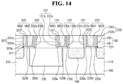
- FIG. 14 is a view provided to explain a semiconductor device, according to some exemplary embodiments.
- FIG. 15 is a view provided to explain a semiconductor device, according to some exemplary embodiments.
- FIG. 16 is a top view provided to explain a semiconductor device, according to some exemplary embodiments.
- FIG. 17 are cross sectional views taken on lines A-A and D-D of FIG. 16 , according to certain disclosed embodiments;
- FIG. 18 is a view provided to explain a semiconductor device, according to some exemplary embodiments.
- FIG. 19 is a view provided to explain a semiconductor device, according to some exemplary embodiments.
- FIG. 20 is a block diagram of an SoC system comprising a semiconductor device, according to certain exemplary embodiments.
- spatially relative terms such as “beneath,” “below,” “lower,” “above,” “upper” and the like, may be used herein for ease of description to describe one element or feature's relationship to another element(s) or feature(s) as illustrated in the figures. It will be understood that the spatially relative terms are intended to encompass different orientations of the device in use or operation in addition to the orientation depicted in the figures. For example, if the device in the figures is turned over, elements described as “below” or “beneath” other elements or features would then be oriented “above” the other elements or features. Thus, the exemplary term “below” can encompass both an orientation of above and below. The device may be otherwise oriented (rotated 90 degrees or at other orientations) and the spatially relative descriptors used herein interpreted accordingly.
- Example embodiments may be described herein with reference to cross-sectional illustrations that are schematic illustrations of idealized example embodiments (and intermediate structures). As such, variations from the shapes of the illustrations as a result, for example, of manufacturing techniques and/or tolerances, are to be expected. Thus, example embodiments should not be construed as limited to the particular shapes of regions illustrated herein but are to include deviations in shapes that result, for example, from manufacturing. For example, an implanted region illustrated as a rectangle will typically have rounded or curved features and/or a gradient of implant concentration at its edges rather than a binary change from implanted to non-implanted region. Likewise, a buried region formed by implantation may result in some implantation in the region between the buried region and the surface through which the implantation takes place. Thus, the regions illustrated in the figures are schematic in nature, their shapes are not intended to limit the scope of the example embodiments.
- orientation, layout, location, shapes, sizes, amounts, or other measures do not necessarily mean an exactly identical orientation, layout, location, shape, size, amount, or other measure, but are intended to encompass nearly identical orientation, layout, location, shapes, sizes, amounts, or other measures within acceptable variations that may occur, for example, due to manufacturing processes.
- the term “substantially” may be used herein to reflect this meaning. For example, items described as “substantially the same,” “substantially equal,” or “substantially planar,” may be exactly the same, equal, or planar, or may be the same, equal, or planar within acceptable variations that may occur, for example, due to manufacturing processes.
- the semiconductor devices described herein may be part of an electronic device, such as a semiconductor memory chip or semiconductor logic chip, a stack of such chips, a semiconductor package including a package substrate and one or more semiconductor chips, a package-on-package device, or a semiconductor memory module, for example.
- the semiconductor device may be part of a volatile or non-volatile memory.
- a chip or package that includes the semiconductor devices may also be referred to generally as a semiconductor device.
- FIGS. 1 to 4B a semiconductor device according to certain exemplary embodiments will be explained with reference to FIGS. 1 to 4B .
- FIG. 1 is a top view provided to explain a semiconductor device according to some exemplary embodiments.
- FIG. 2 is a cross sectional view taken along line A-A of FIG. 1 .
- FIG. 3A is a view illustrating a first gate spacer from which the first gate electrode of FIG. 2 is omitted, and FIG. 3B illustrates the first gate electrode of FIG. 2 separately.
- FIGS. 4A and 4B are cross sectional views taken along line B-B of FIG. 1 .
- a semiconductor device may include a channel region having a fin-type pattern shape, but exemplary embodiments are not limited thereto. Accordingly, the semiconductor device may include a channel region having a wire-pattern shape instead of the fin-type pattern shape.
- a semiconductor device includes a fin-type field effect transistor (FINFET) utilizing a fin-type pattern
- exemplary embodiments are not limited thereto. Accordingly, a semiconductor device according to exemplary embodiments may include a planar transistor.
- the semiconductor device may include a first fin-type pattern 110 , a first gate electrode 120 , a second gate electrode 220 , first gate spacers 131 , 132 , second gate spacers 231 , 232 , a lower interlayer insulating film 181 , and an upper interlayer insulating film 182 .
- the semiconductor device may include a substrate 100 .
- the substrate 100 may be a bulk silicon or a silicon-on-insulator (SOI), for example.
- the substrate 100 may be a silicon substrate, or may include other substance such as silicon germanium, indium antimonide, lead telluride compound, indium arsenide, indium phosphide, gallium arsenide, or gallium antimonide.
- the substrate 100 may be a base substrate having an epitaxial layer formed thereon.
- the first fin-type pattern 110 may protrude from the substrate 100 .
- the first fin-type pattern 110 may extend longitudinally in a first direction X 1 that is perpendicular to a second direction Y 1 .
- first fin-type pattern 110 may refer to an active pattern used in a multigate transistor.
- the first fin-type pattern 110 may be formed as the channels are connected with each other along three surfaces of the fin, or alternatively, may be formed as the channels formed on two opposing surfaces of the fin.
- the first fin-type pattern 110 may be a part of the substrate 100 , or may include an epitaxial layer grown on the substrate 100 .
- the first fin-type pattern 110 may protrude from the substrate because it is an epitaxial layer extending above part of the substrate.
- the first fin-type pattern 110 may protrude from the substrate because it is part of the substrate that protrudes from a lower part of the substrate.
- the first fin-type pattern 110 may include an element semiconductor material such as silicon or germanium, for example. Further, the first fin-type pattern 110 may include a compound semiconductor such as, for example, IV-IV group compound semiconductor or III-V group compound semiconductor.
- the first fin-type pattern 110 may be a binary compound or a ternary compound including, for example, at least two or more of carbon (C), silicon (Si), germanium (Ge), and tin (Sn), or the above-mentioned binary or ternary compound doped with IV group element.
- the first fin-type pattern 110 may be a binary compound, a ternary compound, or a quaternary compound formed by a combination of a III group element, which may be at least one of aluminum (Al), gallium (Ga), and indium (In), with a V group element which may be one of phosphorus (P), arsenic (As) and antimony (Sb).
- a III group element which may be at least one of aluminum (Al), gallium (Ga), and indium (In)
- a V group element which may be one of phosphorus (P), arsenic (As) and antimony (Sb).
- the first fin-type pattern 110 may be a silicon fin-type pattern which includes silicon.
- a first field insulating film 105 may be formed on the substrate 100 .
- the first field insulating film 105 may partially cover a side surface of the first fin-type pattern 110 . Accordingly, an upper surface of the first fin-type pattern 110 may protrude upward higher than an upper surface of the first field insulating film 105 disposed on the long side of the first fin-type pattern 110 .
- the first field insulating film 105 may be disposed along both, opposite side surfaces of the first fin-type pattern 110 in the first direction X 1 , and an upper surface of the first fin-type pattern 110 may protrude above the first field insulating film 105 .
- the first fin-type pattern 110 may be defined by the first field insulating film 105 on the substrate 100 .
- the first field insulating film 105 may include, for example, oxide film, nitride film, oxynitride film, or a combination thereof.
- the first gate electrode 120 may extend in the second direction Y 1 .
- the first gate electrode 120 may be formed to intersect the first fin-type pattern 110 .
- the first gate electrode 120 may be formed to pass over or cross the first fin-type pattern 110 .
- the first gate electrode 120 may be formed on the first fin-type pattern 110 and the first field insulating film 105 .
- the first gate electrode 120 may surround the first fin-type pattern 110 protruding upward higher than the upper surface of the first field insulating film 105 .
- the first gate electrode 120 may surround at least portions of the first fin-type pattern 110 and may cover portions of the first field insulating film 105 , and an upper surface of the first gate electrode 120 may protrude above the first fin-type pattern 110 and the first field insulating film 105 .
- the first gate electrode 120 may include a first sidewall 120 a and a second sidewall 120 c opposed to each other.
- the first gate electrode 120 may include a bottom surface 120 b which connects the first sidewall 120 a of the first gate electrode with the second sidewall 120 c of the first gate electrode, and extends along the upper surface of the first fin-type pattern 110 .
- the first sidewall 120 a and the second sidewall 120 c may extend in an upwards direction, perpendicular to the first and second directions X 1 and Y 1
- the bottom surface 120 b may extend in a direction parallel to the first or second directions X 1 and Y 1 .
- the second gate electrode 220 may extend in the second direction Y 1 .
- the second gate electrode 220 may be formed on the first fin-type pattern 110 so as to intersect the first fin-type pattern 110 .
- the second gate electrode 220 may be formed to pass over or cross the first fin-type pattern 110 .
- the second gate electrode 220 may be formed adjacent to the first gate electrode 120 . No other gate electrode intersecting the first fin-type pattern 110 may be formed between the second gate electrode 220 and the first gate electrode 120 .
- the second gate electrode 220 may include a first sidewall 220 a and a second sidewall 220 c opposed to each other.
- the second gate electrode 220 may include a bottom surface 220 b which connects the first sidewall 220 a of the second gate electrode with the second sidewall 220 c of the second gate electrode, and extends along the upper surface of the first fin-type pattern 110 .
- the first sidewall 220 a and the second sidewall 220 c may extend in an upwards direction, perpendicular to the first and second directions X 1 and Y 1
- the bottom surface 220 b may extend in a direction parallel to the first or second directions X 1 and Y 1 .
- the first gate electrode 120 may include metal layers MG 1 , MG 2 .
- the first gate electrode 120 may include a stack of two or more metal layers MG 1 , MG 2 , as illustrated.
- the first metal layer MG 1 plays a role of adjusting a work function
- the second metal layer MG 2 plays a role of filling a space defined by the first metal layer MG 1 .
- the first metal layer MG 1 may include at least one of, for example, TiN, WN, TiAl, TiAlN, TaN, TiC, TaC, TaCN, TaSiN and a combination thereof, but not limited thereto.
- the second metal layer MG 2 may include at least one of, for example, W, Al, Cu, Co, Ti, Ta, poly-Si, SiGe and a metal alloy, but not limited thereto.
- the second gate electrode 220 may include metal layers MG 3 , MG 4 .
- the second gate electrode 220 may include a stack of two or more metal layers MG 3 , MG 4 , as illustrated.
- the third metal layer MG 3 plays a role of adjusting a work function
- the fourth metal layer MG 4 plays a role of filling a space defined by the first metal layer MG 3 .
- Description of the second gate electrode 220 may be similar to that of the first gate electrode 120 .
- the first gate electrode 120 and the second gate electrode 220 may be formed by replacement process (or gate last process), but not limited thereto.
- the first gate spacers 131 , 132 may be disposed on sidewalls of the first gate electrode 120 .
- the first gate spacers 131 , 132 may include a first one-side spacer 131 disposed on the first sidewall 120 a of the first gate electrode, and a first other-side spacer 132 disposed on the second sidewall 120 c of the first gate electrode.
- the first one-side spacer 131 and the first other-side spacer 132 may define a first trench 121 .
- the first sidewall 121 a of the first trench may be defined by the first one-side spacer 131
- the second sidewall 121 c of the first trench may be defined by the first other-side spacer 132 .
- the bottom surface 121 b of the first trench may be defined by connecting the first sidewall 121 a of the first trench with the second sidewall 121 c of the first trench.
- the bottom surface 121 b of the first trench may be a top surface of the first fin-type pattern 110 .
- the first gate spacers 131 , 132 may include lower portions 131 b , 132 b , and upper portions 131 a , 132 a .
- the first one-side spacer 131 may include the lower portion 131 b and the upper portion 131 a
- the first other-side spacer 132 may include the lower portion 132 b and the upper portion 132 a.
- the second gate spacers 231 , 232 may be disposed on sidewalls of the second gate electrode 220 .
- the second gate spacers 231 , 232 may include a second one-side spacer 231 disposed on the first sidewall 220 a of the second gate electrode, and a second other-side spacer 232 disposed on the second sidewall 220 c of the second gate electrode.
- the second one-side spacer 231 and the second other-side spacer 232 may define a second trench 221 .
- the first sidewall 221 a of the second trench may be defined by the second one-side spacer 231
- the second sidewall 221 c of the second trench may be defined by the second other-side spacer 232 .
- the bottom surface 221 b of the second trench may be defined by connecting the first sidewall 221 a of the second trench with the second sidewall 221 c of the second trench.
- the bottom surface 221 b of the second trench may be a top surface of the first fin-type pattern 110 .
- the second gate spacers 231 , 232 may include lower portions 231 b , 232 b , and upper portions 231 a , 232 a .
- the second one-side spacer 231 may include the lower portion 231 b and the upper portion 231 a
- the second other-side spacer 232 may include the lower portion 232 b and the upper portion 232 a.
- the first gate electrode 120 may be formed by filling the first trench 121 defined by the first gate spacers 131 , 132 .
- the second gate electrode 220 may be formed by filling the second trench 221 defined by the second gate spacers 231 , 232 .
- the first gate spacers 131 , 132 and the second gate spacers 231 , 232 may each include at least one of, for example, silicon nitride (SiN), silicon oxynitride (SiON), silicon oxide (SiO 2 ), silicon oxycarbonitride (SiOCN), and a combination thereof.
- a first gate insulating film 125 may be formed between the first fin-type pattern 110 and the first gate electrode 120 .
- the first gate insulating film 125 may be formed along the profile of the first fin-type pattern 110 protruding upward higher than the first field insulating film 105 .
- the first gate insulating film 125 may formed on top surfaces of the first field insulating film 105 and the first fin-type pattern 110 , and an upper surface of the first gate insulating film 125 may protrude above the first fin-type pattern 110 and the first field insulating film 105 .
- the first gate insulating film 125 may be disposed between the first gate electrode 120 and the first field insulating film 105 .
- the first gate insulating film 125 may be formed along the sidewalls and the bottom surface of the first trench 121 .
- the first gate insulating film 125 may be formed between the first gate spacers 131 , 132 and the first gate electrode 120 .
- an interfacial layer 126 may be additionally formed between the first gate insulating film 125 and the first fin-type pattern 110 .
- an interfacial layer may also be additionally formed between the first gate insulating film 125 and the first fin-type pattern 110 .
- the interfacial layer 126 may be formed along the profile of the first fin-type pattern 110 which protrudes higher than the upper surface of the first field insulating film 105 , although exemplary embodiments are not limited thereto.
- the interfacial layer 126 may be formed between the first fin-type pattern 110 and the first gate insulating film 125 over regions in which the first field insulating film 105 is not formed.
- the interfacial layer 126 may extend along the upper surface of the first field insulating film 105 according to a method of forming the interfacial layer 126 .
- the interfacial layer 126 may extend from one edge of the upper surface of the first field insulating film 105 to another edge of the upper surface of the first field insulating film 105 .
- a second gate insulating film 225 may be formed between the first fin-type pattern 110 and the second gate electrode 220 .
- the second gate insulating film 225 may be disposed between the second gate electrode 220 and the first field insulating film 105 .
- the second gate insulating film 225 may be formed along the sidewalls and the bottom surface of the second trench 221 .
- the second gate insulating film 225 may be formed along the profile of the first fin-type pattern 110 protruding upward higher than the first field insulating film 105 .
- the second gate insulating film 225 may formed on top surfaces of the first field insulating film 105 and the first fin-type pattern 110 , and an upper surface of the second gate insulating film 225 may protrude above the first fin-type pattern 110 and the first field insulating film 105 .
- the second gate insulating film 225 may be formed between the second gate spacers 231 , 232 and the second gate electrode 220 . Description of the second gate insulating film 225 may be similar to that of the first gate insulating film 125 .
- the first gate insulating film 125 and the second gate insulating film 225 may include a high-k dielectric material having a higher dielectric constant than a silicon oxide film.
- the first gate insulating film 125 and the second gate insulating film 225 may include one or more of hafnium oxide, hafnium silicon oxide, lanthanum oxide, lanthanum aluminum oxide, zirconium oxide, zirconium silicon oxide, tantalum oxide, titanium oxide, barium strontium titanium oxide, barium titanium oxide, strontium titanium oxide, yttrium oxide, aluminum oxide, lead scandium tantalum oxide, and lead zinc niobate, but not limited thereto.
- First source/drain regions 140 may be formed on both sides of the first gate electrode 120 and on both sides of the second gate electrode 220 .
- first source/drain regions 140 may be formed between the first gate electrode 120 and an adjacent second gate electrode 220 .
- the first source/drain regions 140 may be impurity regions formed within the first fin-type pattern 110 , but exemplary embodiments are not limited thereto. Accordingly, the first source/drain regions 140 may include an epitaxial layer formed on the first fin-type pattern 110 or formed within the first fin-type pattern 110 .
- first source/drain regions 140 may be elevated source/drain regions including an upper surface which is protruded upward higher than the upper surface of the first fin-type pattern 110 .
- top surfaces of the first source/drain regions 140 may be higher than an upper surface of the first fin-type pattern 110 .
- the interlayer insulating film 180 may be formed on the substrate 100 .
- the interlayer insulating film 180 may cover the first fin-type pattern 110 , the first source/drain regions 140 , and the first field insulating film 105 .
- the interlayer insulating film 180 may be formed above the substrate 100 and on one or more of the first fin-type pattern 110 , the first source/drain regions 140 , and the first field insulating film 105 .
- the interlayer insulating film 180 may surround the sidewalls of the first gate electrode 120 and the second gate electrode 220 . In some embodiments, the interlayer insulating film 180 may surround the outer sidewalls of the first gate spacers 131 , 132 and the outer sidewalls of the second gate spacers 231 , 232 .
- the interlayer insulating film 180 may include a lower interlayer insulating film 181 and an upper interlayer insulating film 182 stacked on the substrate 100 in a sequential order.
- the lower interlayer insulating film 181 may be formed on the first fin-type pattern 110 .
- the lower interlayer insulating film 181 may overlap with the lower portions 131 b , 132 b of the first gate spacers 131 , 132 , and the lower portions 231 b , 232 b of the second gate spacers 231 , 232 .
- the lower interlayer insulating film 181 may be adjacent to the lower portions 131 b , 132 b of the first gate spacers 131 , 132 , and adjacent to the lower portions 231 b , 232 b of the second gate spacers 231 , 232 .
- the lower interlayer insulating film 181 may surround sidewalls of the lower portion 131 b of the first one-side spacer 131 , the lower portion 132 b of the first other-side spacer 132 , the lower portion 231 b of the second one-side spacer 231 , and the lower portion 232 b of the second other-side spacer 232 .
- the portions of the first gate spacers 131 , 132 and the second gate spacers 231 , 232 with the sidewalls thereof surrounded by the lower interlayer insulating film 181 may be defined into the lower portion 131 b of the first one-side spacer 131 , the lower portion 132 b of the first other-side spacer 132 , the lower portion 231 b of the second one-side spacer 231 , and the lower portion 232 b of the second other-side spacer 232 .
- the lower interlayer insulating film 181 may include silicon oxide, silicon nitride, silicon oxynitride, flowable oxide (FOX), Tonen silazen (TOSZ), undoped silica glass (USG), borosilica glass (BSG), phosphosilica glass (PSG), borophosphosilica glass (BPSG), plasma enhanced tetraethyl orthosilicate (PETEOS), fluoride silicate glass (FSG), carbon doped silicon oxide (CDO), xerogel, aerogel, amorphous fluorinated carbon, organo silicate glass (OSG), parylene, bis-benzocyclobutenes (BCB), SiLK, polyimide, porous polymeric material, or a combination thereof, but not limited thereto.
- FOX Tonen silazen
- USG borosilica glass
- PSG phosphosilica glass
- BPSG borophosphosilica glass
- PETEOS plasma enhanced tetraethyl orthosilicate
- the upper interlayer insulating film 182 may be formed on the lower interlayer insulating film 181 .
- the upper interlayer insulating film 182 may overlap with the upper portions 131 a , 132 a of the first gate spacers 131 , 132 , and the upper portions 231 a , 232 a of the second gate spacers 231 , 232 .
- the upper interlayer insulating film 182 may be adjacent to the upper portions 131 a , 132 a of the first gate spacers 131 , 132 , and adjacent to the upper portions 231 a , 232 a of the second gate spacers 231 , 232 .
- the upper interlayer insulating film 182 may surround sidewalls of the upper portion 131 a of the first one-side spacer 131 , the upper portion 132 a of the first other-side spacer 132 , the upper portion 231 a of the second one-side spacer 231 , and the upper portion 232 a of the second other-side spacer 232 .
- the portion with the sidewalls thereof surrounded by the upper interlayer insulating film 182 may be defined into the upper portion 131 a of the first one-side spacer 131 , the upper portion 132 a of the first other-side spacer 132 , the upper portion 231 a of the second one-side spacer 231 , and the upper portion 232 a of the second other-side spacer 232 .
- the upper surface of the first gate electrode 120 and the upper surface of the second gate electrode 220 may be on the same plane as the upper surface of the upper interlayer insulating film 182 , but exemplary embodiments are not limited thereto.
- capping patterns may be formed on the upper surfaces of the first gate electrode 120 and the second gate electrode 220 , respectively, in which case the upper surface of the first gate electrode 120 and the upper surface of the second gate electrode 220 may be lower than the upper surface of the upper interlayer insulating film 182 .
- the upper interlayer insulating film 182 may include silicon oxide, silicon nitride, silicon oxynitride, flowable oxide (FOX), Tonen silazen (TOSZ), undoped silica glass (USG), borosilica glass (BSG), phosphosilica glass (PSG), borophosphosilica glass (BPSG), plasma enhanced tetraethyl orthosilicate (PETEOS), fluoride silicate glass (FSG), carbon doped silicon oxide (CDO), xerogel, aerogel, amorphous fluorinated carbon, organo silicate glass (OSG), parylene, bis-benzocyclobutenes (BCB), SiLK, polyimide, porous polymeric material, or a combination thereof, but not limited thereto.
- FOX Tonen silazen
- USG borosilica glass
- PSG phosphosilica glass
- BPSG borophosphosilica glass
- PETEOS plasma enhanced tetraethyl orthosilicate
- the lower interlayer insulating film 181 is not interposed between the upper interlayer insulating film 182 and the upper portions 131 a , 132 a of the first gate spacers 131 , 132 , nor between the upper interlayer insulating film 182 and the upper portions 231 a , 232 a of the second gate spacers 231 , 232 .
- the boundary surface between the lower interlayer insulating film 181 and the upper interlayer insulating film 182 may be a flat surface.
- the lower surface of the lower interlayer insulating film 181 and the upper surface of the upper interlayer insulating film 182 may be planar surfaces.
- the height from the substrate 100 to the upper surface of the interlayer insulating film 180 may be substantially the same as the height from the substrate 100 to the uppermost portions of the first gate spacers 131 , 132 . Further, the height from the substrate 100 to the upper surface of the interlayer insulating film 180 may be substantially the same as the height from the substrate 100 to the uppermost portions of the second gate spacers 231 , 232 . In some embodiments, a thickness of the interlayer insulating film 180 may be the same as a thickness or height of the first gate spacers 131 , 132 , and the thickness of the interlayer insulating film 180 may be the same as a thickness or height of the second gate spacers 231 , 232 .
- the stress characteristic of the lower interlayer insulating film 181 may be different from the stress characteristic of the upper interlayer insulating film 182 .
- the upper interlayer insulating film 182 may have a compressive stress characteristic. Conversely, when the lower interlayer insulating film 181 has a compressive stress characteristic, the upper interlayer insulating film 182 may have a tensile stress characteristic.
- tensile stress characteristic may refer to the interlayer insulating film having a tension that pulls the gate electrode or the gate spacers toward the interlayer insulating film
- compressive stress characteristic may refer to the interlayer insulating film having a tension that pushes the gate electrode or the gate spacers away from the interlayer insulating film.
- the gate spacers are subject to a force that acts in a direction from the gate electrode to the interlayer insulating film.
- the gate spacers are subject to a force that acts in a direction from the interlayer insulating film to the gate electrode.
- the interlayer insulating film 180 which includes the lower interlayer insulating film 181 and the upper interlayer insulating film 182 having different stress characteristics from each other, may have overall stress characteristic that varies according to differences between the lower interlayer insulating film 181 and the upper interlayer insulating film 182 , such as, for example, different thicknesses, different volumes, etc.
- the lower interlayer insulating film 181 and the upper interlayer insulating film 182 may include different materials from each other, or may include the same material.
- the conditions for forming the lower interlayer insulating film 181 , including heat treatment condition, and the conditions for forming the upper interlayer insulating film 182 , including heat treatment condition may be different from each other. Accordingly, the lower interlayer insulating film 181 and the upper interlayer insulating film 182 can have different stress characteristics from each other.
- the first sidewall 121 a of the first trench 121 may have a slope at a first angle a 1 with respect to the bottom surface 121 b of the first trench 121 .
- the second sidewall 121 c of the first trench 121 may have a slope at a second angle a 2 with respect to the bottom surface 121 b of the first trench 121 .
- the first angle a 1 and the second angle a 2 may be obtuse angles exceeding a right angle.
- the width of the first trench 121 may increase as a distance from the upper surface of the substrate 100 increases.
- the width of the first trench 121 may increase in a direction moving from the bottom surface 121 b of the first trench 121 to an upper portion of the first trench 121 .
- the width of the first trench 121 may be the distance between the first sidewall 121 a and the second sidewall 121 c.
- the degree of tensile stress of the lower interlayer insulating film 181 may be greater than the degree of compressive stress of the upper interlayer insulating film 182 .
- the first sidewall 121 a of the first trench and the second sidewall 121 c of the first trench may have slopes at obtuse angles with respect to the bottom surface 121 b of the first trench 121 .
- the first sidewall 121 a of the first trench and the second sidewall 121 c of the first trench may have slopes at acute angles, rather than obtuse angles, with respect to the bottom surface 121 b of the first trench 121 .
- the first sidewall 120 a of the first gate electrode 120 may have a slope at a third angle b 1 with respect to a surface facing the bottom surface 120 b of the first gate electrode 120 .
- the second sidewall 120 c of the first gate electrode 120 may have a slope at a fourth angle b 2 with respect to a surface facing the bottom surface 120 b of the first gate electrode 120 .
- the third angle b 1 and the fourth angle b 2 may be acute angles that are smaller than the right angle.
- the width of the first gate electrode 120 may increase as a distance from the upper surface of the substrate 100 increases.
- the width of the first gate electrode 120 may increase in a direction from the bottom surface 120 b of the first gate electrode to the upper surface of the first gate electrode 120 .
- the width of the first gate electrode 120 may be the distance between the first sidewall 120 a and the second sidewall 120 c.
- each of the first sidewall 120 a , the second sidewall 120 c , and the bottom surface 120 b are illustrated as planes, and each of the first sidewall 120 a and the second sidewall 120 c are illustrated as intersecting with the bottom surface 120 b along lines.
- the region where the first sidewall 120 a of the first gate electrode 120 and the bottom surface 120 b of the first gate electrode 120 meet, and the region where the second sidewall 120 c of the first gate electrode 120 and the bottom surface 120 b of the first gate electrode 120 meet may have rounded shapes, but it is apparent to those skilled in the art that the slope of the first sidewall 120 a of the first gate electrode 120 and the slope of the second sidewall 120 c of the first gate electrode 120 may still retain a slope relative to the bottom surface 120 b of the first gate electrode 120 .
- the second gate electrode 220 and the second trench 221 will not be redundantly described as these may be substantially similar to the first gate electrode 120 and the first trench 121 described above.
- the sidewall of the trench has a positive slope when the sidewall of the trench has a slope at an obtuse angle with the bottom surface of the trench.
- the sidewall of the gate electrode has a positive slope when the sidewall of the gate electrode has a slope at an obtuse angle with the bottom surface of the gate electrode.
- the first sidewall 120 a of the first gate electrode 120 , the second sidewall 120 c of the first gate electrode 120 , the first sidewall 220 a of the second gate electrode 220 , and the second sidewall 220 c of the second gate electrode 220 each may have positive slopes.
- FIG. 5 is a view provided to explain a semiconductor device according to some exemplary embodiments.
- FIG. 6 is a view provided to explain a semiconductor device according to some exemplary embodiments.
- FIGS. 5 and 6 are cross sectional views taken on line A-A of FIG. 1 .
- the first sidewall 120 a of the first gate electrode 120 and the second sidewall 120 c of the first gate electrode 120 may have slopes at a right angle with the bottom surface 120 b of the first gate electrode 120 .
- first sidewall 220 a of the second gate electrode 220 and the second sidewall 220 c of the second gate electrode 220 may have slopes at right angles with the bottom surface 220 b of the second gate electrode 220 .
- the width of the first gate electrode 120 may remain substantially constant as a distance from the upper surface of the substrate 100 increases.
- the width of the first gate electrode 120 may remain the same in a direction moving from the bottom surface 120 b of the first gate electrode 120 to an upper portion of the first gate electrode 120 .
- the width of the first gate electrode 120 may be the distance between the first sidewall 120 a and the second sidewall 120 c.
- the first sidewall 121 a of the first trench 121 may have a slope at a right angle with respect to the bottom surface 121 b of the first trench 121
- the second sidewall 121 c of the first trench 121 may have a slope at a right angle with respect to the bottom surface of the first trench 121 .
- Description of the second trench 221 may be similar to that of the first trench 121 .
- the first sidewall 120 a of the first gate electrode 120 and the second sidewall 120 c of the first gate electrode 120 may have slopes at an acute angle with the bottom surface 120 b of the first gate electrode 120 .
- first sidewall 220 a of the second gate electrode 220 and the second sidewall 220 c of the second gate electrode 220 may have slopes at an acute angle with the bottom surface 220 b of the second gate electrode 220 .
- the width of the first gate electrode 120 and the width of the second gate electrode 220 may decrease as a distance from the upper surface of the substrate 100 increases.
- the width of the first gate electrode 120 may decrease in a direction from the bottom surface 120 b of the first gate electrode to the upper surface of the first gate electrode 120 .
- the width of the second gate electrode 220 may decrease in a direction from the bottom surface 220 b of the second gate electrode to the upper surface of the second gate electrode 220 .
- the width of the first gate electrode 120 may be the distance between the first sidewall 120 a and the second sidewall 120 c of the first gate electrode 120
- the width of the second gate electrode 220 may be the distance between the first sidewall 220 a and the second sidewall 220 c of the second gate electrode 220 .
- the first sidewall 121 a of the first trench 121 may have a slope at an acute angle with respect to the bottom surface 121 b of the first trench 121
- the second sidewall 121 c of the first trench 121 may have a slope at an acute angle with respect to the bottom surface 121 b of the first trench 121 .
- Description of the second trench 221 may be similar to that of the first trench 121 .
- the first sidewall 120 a of the first gate electrode 120 , the second sidewall 120 c of the first gate electrode 120 , the first sidewall 220 a of the second gate electrode 220 , and the second sidewall 220 c of the second gate electrode 220 each may have negative slopes.
- each of the slopes of the first sidewall 120 a of the first gate electrode 120 , the slope of the second sidewall 120 c of the first gate electrode 120 , the slope of the first sidewall 220 a of the second gate electrode 220 , and the slope of the second sidewall 220 c of the second gate electrode 220 may be acute angles with respect to bottom surfaces of the respective first and second gate electrodes 120 and 220 .
- FIGS. 7A and 7B are views provided to explain a semiconductor device according to some exemplary embodiments. For convenience of explanation, differences that are not explained above with reference to FIG. 5 will be mainly explained below.
- FIGS. 7A and 7B are cross sectional views taken on line A-A of FIG. 1 .
- the boundary between the lower interlayer insulating film 181 and the upper interlayer insulating film 182 may have a curved surface.
- the boundary between the lower interlayer insulating film 181 and the upper interlayer insulating film 182 may have a convex shape relative to the upper surface of the substrate 100 , i.e., to the upper surface of the first fin-type pattern 110 .
- the boundary between the lower interlayer insulating film 181 and the upper interlayer insulating film 182 may have a shape that is rounded or curved in a direction away from the upper surface of the substrate 100 .
- the boundary between the lower interlayer insulating film 181 and the upper interlayer insulating film 182 may have a concave shape relative to the upper surface of the substrate 100 .
- the boundary between the lower interlayer insulating film 181 and the upper interlayer insulating film 182 may have a shape that is rounded or curved in a direction toward the upper surface of the substrate 100 .
- the shape of the boundary between the lower interlayer insulating film 181 and the upper interlayer insulating film 182 may vary depending on, for example, a method of etching the lower interlayer insulating film 181 in the manufacturing process, an etchant used for etching, etc.
- FIG. 8 is a view provided to explain a semiconductor device according to some exemplary embodiments. For convenience of explanation, differences that are not explained above with reference to FIG. 5 will be mainly explained below.
- the upper surfaces of the first gate spacers 131 , 132 and the upper surfaces of the second gate spacers 231 , 232 each may include inclined surfaces having slopes with respect to the upper surface of the upper interlayer insulating film 182 .
- the upper surfaces of the upper portions 131 a , 132 a of the first gate spacers 131 , 132 and the upper surfaces of the upper portions 231 a , 232 a of the second gate spacers 231 , 232 each may include inclined surfaces having slopes at an acute angle with respect to the upper surface of the upper interlayer insulating film 182 .
- the first one-side spacer 131 may include an inclined surface 131 s having a slope at an acute angle with respect to the upper surface of the upper interlayer insulating film 182 .
- the inclined surface 131 s may be included in the upper portion 131 a of the first one-side spacer 131 .
- the inclined surface 131 s of the first one-side spacer 131 may have a slope at a fifth angle c with respect to the upper surface of the upper interlayer insulating film 182 .
- the fifth angle (c) may be an acute angle.
- each of the first other-side spacer 132 , the second one-side spacer 231 , and the second other-side spacer 232 may include inclined surfaces having slopes at an acute angle with respect to the upper surface of the upper interlayer insulating film 182 .
- the inclined surfaces of the first other-side spacer 132 , the second one-side spacer 231 , and the second other-side spacer 232 may be included, respectively, in the upper portion 132 a of the first other-side spacer 132 , the upper portion 231 a of the second one-side spacer 231 , and the upper portion 232 a of the second other-side spacer 232 .
- the boundary between the lower interlayer insulating film 181 and the upper interlayer insulating film 182 may have a convex shape relative to the upper surface of the substrate 100 , i.e., to the upper surface of the first fin-type pattern 110 , but not limited thereto.
- the boundary between the lower interlayer insulating film 181 and the upper interlayer insulating film 182 may have a shape that is rounded or curved in a direction away from the upper surface of the substrate 100 .
- FIG. 9 is a view provided to explain a semiconductor device according to some exemplary embodiments. For convenience of explanation, differences that are not explained above with reference to FIG. 5 will be mainly explained below.
- the semiconductor device may additionally include an etch-stop layer 185 between the interlayer insulating film 180 and the first source/drain region 140 .
- the etch-stop layer 185 may extend along the sidewalls of the first gate spacers 131 , 132 , the second gate spacers 231 , 232 , and the upper surface of the first source/drain region 140 .
- the etch-stop layer 185 may extend between the interlayer insulating film 180 and the first gate spacers 131 , 132 , and between the interlayer insulating film 180 and the second gate spacers 231 , 232 .
- the etch-stop layer 185 may be formed by extending from between the lower interlayer insulating film 181 and a top surface of the first source/drain region 140 , to between the lower interlayer insulating film 181 and the lower portions 131 b , 132 b of the first gate spacers, and then between the upper interlayer insulating film 182 and the upper portions 131 a , 132 a of the first gate spacers.
- a portion of the etch-stop layer 185 extending along the sidewalls of the first gate spacers 131 , 132 and the sidewalls of the second gate spacers 231 , 232 may extend up to the height of the upper surface of the upper interlayer insulating film 182 .
- the lower interlayer insulating film 181 and the upper interlayer insulating film 182 may be stacked in a sequential order on the substrate 100 where the etch-stop layer 185 is formed.
- the etch-stop layer 185 may be disposed on the first source/drain region 140
- the lower interlayer insulating film 181 may be disposed on the etch-stop layer 185
- the upper interlayer insulating film 182 may be disposed on the lower interlayer insulating film 181 .
- the etch-stop layer 185 may include at least one of silicon nitride (SiN), silicon oxynitride (SiON), silicon oxide (SiO 2 ), silicon oxycarbonitride (SiOCN), silicon carbonitride (SiCN), and a combination thereof, but not limited thereto.
- FIG. 10 is a view provided to explain a semiconductor device according to some exemplary embodiments. For convenience of explanation, differences that are not explained above with reference to FIG. 9 will be mainly explained below.
- the upper interlayer insulating film 182 may cover the uppermost portion of the etch-stop layer 185 .
- the etch-stop layer 185 may extend between the lower interlayer insulating film 181 and the lower portions 131 b , 132 b of the first gate spacers, and between the lower interlayer insulating film 181 and the lower portions 231 b , 232 b of the second gate spacers.
- the etch-stop layer 185 may not extend between the upper interlayer insulating film 182 and the upper portions 131 a , 132 a of the first gate spacers 131 , 132 , and between the upper interlayer insulating film 182 and the upper portions 231 a , 232 a of the second gate spacers 231 , 232 .
- a portion of the etch-stop layer 185 extending along the sidewalls of the first gate spacers 131 , 132 and the sidewalls of the second gate spacers 231 , 232 do not extend up to the height of the upper surfaces of the first gate spacers 131 , 132 and the upper surfaces of the second gate spacers 231 , 232 .
- the upper interlayer insulating film 182 may extend over an upper end surface of the etch-stop layer 185 in regions near the upper portions 131 a , 132 a of the first gate spacers 131 , 132 and in regions near the upper portions 231 a , 232 a of the second gate spacers 231 , 232 .
- the height from the upper surface of the substrate 100 to the uppermost portion of the etch-stop layer 185 is less than the height from the upper surface of the substrate 100 to the upper surface of the upper interlayer insulating film 182 .
- the boundary between the lower interlayer insulating film 181 and the upper interlayer insulating film 182 may have a convex shape to the upper surface of the substrate 100 , i.e., to the upper surface of the first fin-type pattern 110 , but is not limited thereto.
- the boundary between the lower interlayer insulating film 181 and the upper interlayer insulating film 182 may have a shape that is rounded or curved in a direction toward the upper surface of the substrate 100 .
- FIG. 11 is a view provided to explain a semiconductor device according to some exemplary embodiments. For convenience of explanation, differences that are not explained above with reference to FIG. 5 will be mainly explained below.
- a semiconductor device may additionally include a channel layer 115 formed between the first fin-type pattern 110 and the first gate electrode 120 , and between the first fin-type pattern 110 and the second gate electrode 220 .
- the channel layer 115 may be formed between the first fin-type pattern 110 and the first gate insulating film 125 , and between the first fin-type pattern 110 and the second gate insulating film 225 .
- the channel layer 115 may be formed on the upper surface of the first fin-type pattern 110 , and below bottom surfaces of the first gate insulating film 125 and the second gate insulating film 225 .
- the channel layer 115 may include a material which is different from the material that forms the first fin-type pattern 110 .
- the channel layer 115 may include silicon germanium which has a greater lattice constant than silicon.
- the channel layer 115 may include, for example, silicon germanium or germanium which has a greater lattice constant than the silicon germanium included in the first fin-type pattern 110 .
- the channel layer 115 may include silicon having a smaller lattice constant than the silicon germanium.
- FIG. 12 is a top view provided to explain a semiconductor device according to some exemplary embodiments.
- FIG. 13 is a cross sectional view taken on line C-C of FIG. 12 .
- FIGS. 1 to 4B will be mainly explained below.
- a semiconductor device may additionally include a second fin-type pattern 310 , a third gate electrode 320 , and third gate spacers 331 , 332 .
- the second fin-type pattern 310 may protrude from the substrate 100 .
- the second fin-type pattern 310 may extend longitudinally in a first direction X 1 .
- the first fin-type pattern 110 and the second fin-type pattern 310 may be aligned in the first direction X 1 .
- the short side of the first fin-type pattern 110 and the short side of the second fin-type pattern 310 may be opposed to each other.
- a short end side of the first fin-type pattern 110 may be adjacent to and face a short end side of the second fin-type pattern 310 .
- the second field insulating film 106 may be formed between the first fin-type pattern 110 and the second fin-type pattern 310 .
- the upper surface of the second field insulating film 106 disposed between the short side of the first fin-type pattern 110 and the short side of the second fin-type pattern 310 may be placed on the same plane as the upper surface of the first fin-type pattern 110 and the upper surface of the second fin-type pattern 310 , or it may be higher.
- the topmost upper surface of the second field insulating film 106 may be on the same plane as the topmost upper surface of the first fin-type pattern 110 and the topmost upper surface of the second fin-type pattern 310 .
- the upper surface of the second field insulating film 106 disposed between the short side of the first fin-type pattern 110 and the short side of the second fin-type pattern 310 may be higher than the upper surface of the first field insulating film 105 , as illustrated in FIG. 4A , disposed at the long side of the first fin-type pattern 110 .
- FIG. 13 illustrates the upper surface of the second field insulating film 106 being a flat or planar surface, but this is only for illustrative purpose and the embodiments are not limited thereto. At least a portion of the upper surface of the second field insulating film 106 between the first gate electrode 120 and the third gate electrode 320 may be recessed from the upper surface of the second field insulating film 106 which overlaps with the first gate electrode 120 . In some embodiments, at least a portion of the upper surface of the second field insulating film 106 may be convex or concave.
- the first gate electrode 120 may be formed on the first fin-type pattern 110 and the second field insulating film 106 .
- a portion of the first gate electrode 120 may intersect or cross over the first fin-type pattern 110 , and the rest of the first gate electrode 120 may be formed on the second field insulating film 106 .
- the first gate electrode 120 may be formed on an end portion of the first fin-type pattern 110 .
- the third gate electrode 320 may be formed on the second fin-type pattern 310 and the second field insulating film 106 . A portion of the third gate electrode 320 may intersect or cross over the second fin-type pattern 310 , and the rest of the third gate electrode 320 may be formed on the second field insulating film 106 . For example, the third gate electrode 320 may be formed on an end portion of the second fin-type pattern 310 .
- the third gate electrode 320 may include a first sidewall 320 a and a second sidewall 320 c opposed to each other.
- the third gate electrode 320 may include a bottom surface 320 b which connects the first sidewall 320 a of the third gate electrode with the second sidewall 320 c of the third gate electrode, and extends along at least a portion of the upper surface of the second fin-type pattern 310 and at least a portion of the upper surface of the second field insulating film 106 .
- the third gate electrode 320 may include metal layers MG 5 , MG 6 .
- the third gate electrode 320 may include a stack of two or more metal layers MG 5 , MG 6 , as illustrated.
- No additional gate electrode may be formed between the first gate electrode 120 and the second gate electrode 220 , and between the first gate electrode 120 and the third gate electrode 320 .
- the second gate electrode 220 and the third gate electrode 320 may be the gate electrodes that are most adjacent to the first gate electrode 120 .
- the distance S 1 between the first gate electrode 120 and the second gate electrode 220 may be different from the distance S 2 between the first gate electrode 120 and the third gate electrode 320 .
- the distance S 1 between the first gate electrode 120 and the second gate electrode 220 may be greater than the distance S 2 between the first gate electrode 120 and the third gate electrode 320 .
- the third gate spacers 331 , 332 may be disposed on sidewalls of the third gate electrode 320 .
- the third gate spacers 331 , 332 may include a third one-side spacer 331 disposed on the first sidewall 320 a of the third gate electrode, and a third other-side spacer 332 disposed on the second sidewall 320 c of the third gate electrode.
- the third one-side spacer 331 and the third other-side spacer 332 may define a third trench 321 .
- the third gate electrode 320 may be formed by filling the third trench 321 defined by the third gate spacers 331 , 332 .
- the third one-side spacer 331 may include the lower portion 331 b and the upper portion 331 a
- the third other-side spacer 332 may include the lower portion 332 b and the upper portion 332 a.
- the third gate insulating film 325 may be formed along the sidewall and the bottom surface of the third trench 321 .
- the third gate electrode 320 may be formed on the third gate insulating film 325 .
- the lower interlayer insulating film 181 may overlap with the lower portions 331 b , 332 b of the third gate spacers 331 , 332 .
- the lower interlayer insulating film 181 may be adjacent to the lower portions 331 b , 332 b of the third gate spacers 331 , 332 .
- the lower interlayer insulating film 181 may surround the lower portion 331 b of the third one-side spacer 331 and the sidewall of the lower portion 332 b of the third other-side spacer 332 .
- the upper interlayer insulating film 182 may overlap with the upper portions 331 a , 332 a of the third gate spacers 331 , 332 .
- the upper interlayer insulating film 182 may surround the upper portion 331 a of the third one-side spacer 331 and the sidewall of the upper portion 332 a of the third other-side spacer 332 .
- the lower interlayer insulating film 181 may not be interposed between the upper interlayer insulating film 182 and the upper portions 331 a , 332 a of the third gate spacers 331 , 332 .
- the first sidewall 220 a of the second gate electrode and the second sidewall 220 c of the second gate electrode 220 may have slopes at a right angle with respect to the bottom surface 220 b of the second gate electrode 220 .
- the second sidewall 120 c of the first gate electrode 120 which is closer to the second gate electrode 220 than the first sidewall 120 a of the first gate electrode 120 , may also have a slope at a right angle with respect to the bottom surface 120 b of the first gate electrode 120 .
- first sidewall 120 a of the first gate electrode 120 may have a slope at an acute angle with respect to the bottom surface 120 b of the first gate electrode 120 .
- the slope of the first sidewall 120 a of the first gate electrode and the slope of the second sidewall 120 c of the first gate electrode may be different from each other.
- the slope of the first sidewall 120 a of the first gate electrode 120 and the slope of the second sidewall 120 c of the first gate electrode 120 may be different.
- the second sidewall 320 c of the third gate electrode 320 adjacent to the first gate electrode 120 may have a slope at an acute angle with respect to the bottom surface 320 b of the third gate electrode 320 , and unlike the second sidewall 320 c of the third gate electrode 320 , the first sidewall 320 a of the third gate electrode 320 may have a slope at a right angle, although exemplary embodiments are not limited thereto.
- the slope of the first sidewall 320 a of the third gate electrode 320 and the slope of the second sidewall 320 c of the third gate electrode 320 with respect to the bottom surface 320 b of the third gate electrode 320 may vary according to a distance between the gate electrode adjacent to the third one-side spacer 331 and the third gate electrode 320 .
- the second field insulating film 106 is formed between the first fin-type pattern 110 and the second fin-type pattern 310 , exemplary embodiments are not limited thereto.
- the first fin-type pattern 110 and the second fin-type pattern 310 may be one integrated fin-type pattern.
- FIG. 14 is a view provided to explain a semiconductor device according to some exemplary embodiments.
- FIG. 15 is a view provided to explain a semiconductor device according to some exemplary embodiments.
- the first sidewall 120 a of the first gate electrode 120 may have a slope at an obtuse angle with respect to the bottom surface 120 b of the first gate electrode 120 .
- the second sidewall 120 c of the first gate electrode 120 which is closer to the second gate electrode 220 than the first sidewall 120 a of the first gate electrode 120 , may have a slope at a right angle with respect to the bottom surface 120 b of the first gate electrode 120 .
- first sidewall 220 a of the second gate electrode 220 and the second sidewall 220 c of the second gate electrode 220 may have slopes at a right angle with respect to the bottom surface 220 b of the second gate electrode 220 .
- the upper surface of the second field insulating film 106 may be lower than the upper surface of the first fin-type pattern 110 and the upper surface of the second fin-type pattern 310 .
- the first gate electrode 120 may be formed to surround an end of the first fin-type pattern 110 which protrudes upward higher than the second field insulating film 106
- the third gate electrode 320 may be formed to surround an end of the second fin-type pattern 310 which protrudes upward higher than the second field insulating film 106 .
- the second field insulating film 106 may include a protruding portion at a contact portion with the short side of the first fin-type pattern 110 or the short side of the second fin-type pattern 310 .
- the upper surface of the protruding portion may be on the same plane as the upper surface of the first fin-type pattern 110 and the upper surface of the second fin-type pattern 310 , or it may be higher.
- FIG. 16 is a top view provided to explain a semiconductor device according to some exemplary embodiments.
- FIG. 17 is a cross sectional views taken on lines A-A and D-D of FIG. 16 .
- FIG. 17 For reference, the cross sectional view taken on line A-A of FIG. 17 is illustrated in a similar manner as the view of FIG. 5 for convenience of explanation only. Accordingly, exemplary embodiments are not limited to such illustration. Further, for convenience of explanation, elements or operations redundant to those already described above with reference to FIGS. 1 to 11 will not be described or will be described succinctly for the sake of brevity.
- the semiconductor device may include a first fin-type pattern 110 , a first gate electrode 120 , a second gate electrode 220 , first gate spacers 131 , 132 , second gate spacers 231 , 232 , a third fin-type pattern 410 , a fourth gate electrode 420 , a fifth gate electrode 520 , fourth gate spacers 431 , 432 , fifth gate spacers 531 , 532 , a lower interlayer insulating film 181 , and an upper interlayer insulating film 182 .
- the substrate 100 may include a first region I and a second region II.
- the first region I and the second region II may be spaced from each other and/or connected with each other.
- the first fin-type pattern 110 In the first region I, the first fin-type pattern 110 , the first gate electrode 120 , the second gate electrode 220 , the first gate spacers 131 , 132 , and the second gate spacers 231 , 232 may be formed.
- a sixth gate electrode 170 intersecting the first fin-type pattern 110 may be additionally formed.
- the sixth gate electrode 170 may be formed to pass over or cross the first fin-type pattern 110 .
- the first gate electrode 120 may be disposed between the second gate electrode 220 and the sixth gate electrode 170 .
- the distance S 1 between the first gate electrode 120 and the second gate electrode 220 may be same as the distance between the first gate electrode 120 and the sixth gate electrode 170 .
- No other gate electrode intersecting the first fin-type pattern 110 may be formed between the sixth gate electrode 170 and the first gate electrode 120 .
- the third fin-type pattern 410 the fourth gate electrode 420 , the fifth gate electrode 520 , the fourth gate spacers 431 , 432 and the fifth gate spacers 531 , 532 may be formed.
- the third fin-type pattern 410 may protrude from the substrate 100 .
- the third fin-type pattern 410 may extend longitudinally in a third direction X 2 .
- the fourth gate electrode 420 may extend in a fourth direction Y 2 .
- the fourth gate electrode 420 may be formed on the third fin-type pattern 410 so as to intersect the third fin-type pattern 410 .
- the fourth gate electrode 420 may include a first sidewall 420 a and a second sidewall 420 c opposed to each other.
- the fourth gate electrode 420 may include a bottom surface 420 b which connects the first sidewall 420 a of the fourth gate electrode with the second sidewall 420 c of the fourth gate electrode, and extends along the upper surface of the third fin-type pattern 410 .
- the fifth gate electrode 520 may extend in the fourth direction Y 2 .
- the fifth gate electrode 520 may be formed on the third fin-type pattern 410 so as to intersect the third fin-type pattern 410 .
- the fifth gate electrode 520 may be formed to pass over or cross the third fin-type pattern 410 .
- No other gate electrode intersecting the third fin-type pattern 410 may be formed between the fifth gate electrode 520 and the fourth gate electrode 420 .
- the fifth gate electrode 520 may include a first sidewall 520 a and a second sidewall 520 c opposed to each other.
- the fifth gate electrode 520 may include a bottom surface 520 b which connects the first sidewall 520 a of the fifth gate electrode 520 with the second sidewall 520 c of the fifth gate electrode 520 , and extends along the upper surface of the third fin-type pattern 410 .
- the fourth gate electrode 420 may include metal layers MG 7 , MG 8 , and the fifth gate electrode 520 may include metal layers MG 9 , MG 10 . As illustrated, the fourth gate electrode 420 and the fifth gate electrode 520 may be stacks of two or more metal layers.
- a seventh gate electrode 470 intersecting the third fin-type pattern 410 may be additionally formed.
- the seventh gate electrode 470 may be formed to pass over or cross the third fin-type pattern 410 .
- the fourth gate electrode 420 may be disposed between the fifth gate electrode 520 and the seventh gate electrode 470 .
- the distance S 3 between the fourth gate electrode 420 and the fifth gate electrode 520 may be same as the distance between the fourth gate electrode 420 and the seventh gate electrode 470 .
- No other gate electrode intersecting the third fin-type pattern 410 may be formed between the seventh gate electrode 470 and the fourth gate electrode 420 .
- the distance S 1 between the first gate electrode 120 and the second gate electrode 220 may be substantially equal to the distance S 3 between the fourth gate electrode 420 and the fifth gate electrode 520 .
- the fourth gate spacers 431 , 432 may include a fourth one-side spacer 431 disposed on the first sidewall 420 a of the fourth gate electrode, and a fourth other-side spacer 432 disposed on the second sidewall 420 c of the fourth gate electrode.
- the fourth one-side spacer 431 and the fourth other-side spacer 432 may define a fourth trench 421 .
- the fourth one-side spacer 431 may include a lower portion 431 b and an upper portion 431 a
- the fourth other-side spacer 432 may include a lower portion 432 b and an upper portion 432 a.
- the fifth gate spacers 531 , 532 may include a fifth one-side spacer 531 disposed on the first sidewall 520 a of the fifth gate electrode 520 , and a fifth other-side spacer 532 disposed on the second sidewall 520 c of the fifth gate electrode 520 .
- the fifth one-side spacer 531 and the fifth other-side spacer 532 may define a fifth trench 521 .
- the fifth one-side spacer 531 may include a lower portion 531 b and an upper portion 531 a
- the fifth other-side spacer 532 may include a lower portion 532 b and an upper portion 532 a.
- the fourth gate insulating film 425 may be formed along the sidewall and the bottom surface of the fourth trench 421
- the fifth gate insulating film 525 may be formed along the sidewall and the bottom surface of the fifth trench 521 .
- the lower interlayer insulating film 181 may overlap with the lower portions 431 b , 432 b of the fourth gate spacers 431 , 432 , and with the lower portions 531 b , 532 b of the fifth gate spacers 531 , 532 .
- the lower interlayer insulating film 181 may surround sidewalls of the lower portion 431 b of the fourth one-side spacer 431 , the lower portion 432 b of the fourth other-side spacer 432 , the lower portion 531 b of the fifth one-side spacer 531 , and the lower portion 532 b of the fifth other-side spacer 532 .
- the upper interlayer insulating film 182 may overlap with the upper portions 431 a , 432 a of the fourth gate spacers 431 , 432 , and with the upper portions 531 a , 532 a of the fifth gate spacers 531 , 532 .
- the upper interlayer insulating film 182 may surround sidewalls of the upper portion 431 a of the fourth one-side spacer 431 , the upper portion 432 a of the fourth other-side spacer 432 , the upper portion 531 a of the fifth one-side spacer 531 , and the upper portion 532 a of the fifth other-side spacer 532 .
- the lower interlayer insulating film 181 is not interposed between the upper interlayer insulating film 182 and the upper portions 431 a , 432 a of the fourth gate spacers 431 , 432 , nor between the upper interlayer insulating film 182 and the upper portions 531 a , 532 a of the fifth gate spacers 531 , 532 .
- the lower interlayer insulating film 181 may have the tensile stress characteristic
- the upper interlayer insulating film 182 may have the compressive stress characteristic
- the height from the upper surface of the first fin-type pattern 110 to the upper surface of the upper interlayer insulating film 182 in the first region I may be substantially equal to the height from the upper surface of the third fin-type pattern 410 to the upper surface of the upper interlayer insulating film 182 in the second region II.
- the upper surface of the first gate electrode 120 and the upper surface of the second gate electrode 220 may be placed on the same plane as the upper surface of the upper interlayer insulating film 182 , and the upper surface of the fourth gate electrode 420 and the upper surface of the fifth gate electrode 520 may be placed on the same plane as the upper surface of the upper interlayer insulating film 182 .
- the thickness t 1 of the lower interlayer insulating film 181 in the first region I may be different from the thickness t 2 of the lower interlayer insulating film 181 in the second region II.
- the thickness t 1 of the lower interlayer insulating film 181 in the first region I may be thinner than the thickness t 2 of the lower interlayer insulating film 181 in the second region II.
- the thickness of the upper interlayer insulating film 182 in the first region I may be thicker than the thickness of the upper interlayer insulating film 182 in the second region II. In some embodiments, however, the thickness of the upper interlayer insulating film 182 in the second region II may be thicker than the thickness of the upper interlayer insulating film 182 in the first region I.
- the ratio of the thickness of the upper interlayer insulating film 182 to the thickness of the lower interlayer insulating film 181 in the first region I may be different from the ratio of the thickness of the upper interlayer insulating film 182 to the thickness of the lower interlayer insulating film 181 in the second region II.
- the ratio of the thickness of the upper interlayer insulating film 182 to the thickness of the lower interlayer insulating film 181 in the first region I may be greater than the ratio of the thickness of the upper interlayer insulating film 182 to the thickness of the lower interlayer insulating film 181 in the second region II.
- the slopes of the sidewalls 120 a , 120 c of the first gate electrode 120 relative to the bottom surface 120 b of the first gate electrode 120 may be different from the slopes of the sidewalls 420 a , 420 c of the fourth gate electrode 420 relative to the bottom surface 420 b of the fourth gate electrode 420 .
- the first sidewall 120 a of the first gate electrode and the second sidewall 120 c of the first gate electrode may have slopes at a right angle with respect to the bottom surface 120 b of the first gate electrode 120 .
- first sidewall 420 a of the fourth gate electrode 420 and the second sidewall 420 c of the fourth gate electrode 420 may have an obtuse angle with respect to the bottom surface 420 b of the fourth gate electrode 420 .
- angles of the sidewalls 420 a , 420 c of the fourth gate electrode 420 relative to the bottom surface 420 b of the fourth gate electrode 420 may be greater than the angles of the sidewalls 120 a , 120 c of the first gate electrode 120 relative to the bottom surface 120 b of the first gate electrode 120 .
- the width of the first gate electrode 120 may remain substantially constant, but the width of the fourth gate electrode 420 may increase.
- the angles of the sidewalls 420 a , 420 c of the fourth gate electrode 420 relative to the bottom surface 420 b of the fourth gate electrode 420 may be greater than the angles of the sidewalls 120 a , 120 c of the first gate electrode 120 relative to the bottom surface 120 b of the first gate electrode 120 .
- first sidewall 120 a of the first gate electrode 120 and the second sidewall 120 c of the first gate electrode 120 may have slopes at an acute angle with the bottom surface 120 b of the first gate electrode 120 .
- the lower interlayer insulating film 181 has the compressive stress characteristic
- the upper interlayer insulating film 182 has the tensile stress characteristic
- the first sidewall 420 a of the fourth gate electrode 420 and the second sidewall 420 c of the fourth gate electrode 420 may make an acute angle with the bottom surface 420 b of the fourth gate electrode 420 .
- FIG. 18 is a view provided to explain a semiconductor device according to some exemplary embodiments. For convenience of explanation, differences that are not explained above with reference to FIGS. 16 and 17 will be mainly explained below.
- the thickness t 1 of the lower interlayer insulating film 181 in the first region I may be thicker than the thickness t 2 of the lower interlayer insulating film 181 in the second region II.
- the thickness of the upper interlayer insulating film 182 in the first region I may be thinner than the thickness of the upper interlayer insulating film 182 in the second region II.
- the ratio of the thickness of the upper interlayer insulating film 182 to the thickness of the lower interlayer insulating film 181 in the first region I may be smaller than the ratio of the thickness of the upper interlayer insulating film 182 to the thickness of the lower interlayer insulating film 181 in the second region II.
- the lower interlayer insulating film 181 may have the tensile stress characteristic
- the upper interlayer insulating film 182 may have the compressive stress characteristic
- the angles of the sidewalls 420 a , 420 c of the fourth gate electrode 420 relative to the bottom surface 420 b of the fourth gate electrode 420 may be smaller than the angles of the sidewalls 120 a , 120 c of the first gate electrode 120 relative to the bottom surface 120 b of the first gate electrode 120 .
- first sidewall 120 a of the first gate electrode 120 and the second sidewall 120 c of the first gate electrode 120 may have slopes at a right angle with respect to the bottom surface 120 b of the first gate electrode 120 .
- first sidewall 420 a of the fourth gate electrode 420 and the second sidewall 420 c of the fourth gate electrode 420 may have slopes at an acute angle with respect to the bottom surface 420 b of the fourth gate electrode 420 .
- the width of the first gate electrode 120 may remain substantially constant, but the width of the fourth gate electrode 420 may decrease as the distance from the upper surface of the substrate 100 increases.
- first sidewall 120 a of the first gate electrode 120 and the second sidewall 120 c of the first gate electrode 120 may have slopes at an obtuse angle with respect to the bottom surface 120 b of the first gate electrode 120 .
- the lower interlayer insulating film 181 may have the compressive stress characteristic
- the upper interlayer insulating film 182 may have the tensile stress characteristic
- the first sidewall 420 a of the fourth gate electrode 420 and the second sidewall 420 c of the fourth gate electrode 420 may make an obtuse angle with the bottom surface 420 b of the fourth gate electrode 420 .
- FIG. 19 is a view provided to explain a semiconductor device according to some exemplary embodiments. For convenience of explanation, differences that are not explained above with reference to FIGS. 16 and 17 will be mainly explained below.
- the distance S 1 between the first gate electrode 120 and the second gate electrode 220 may be different than the distance S 3 between the fourth gate electrode 420 and the fifth gate electrode 520 .
- the distance S 1 between the first gate electrode 120 and the second gate electrode 220 may be smaller than the distance S 3 between the fourth gate electrode 420 and the fifth gate electrode 520 .
- the thickness t 1 of the lower interlayer insulating film 181 in the first region I may be equal to the thickness t 2 of the lower interlayer insulating film 181 in the second region II.
- the ratio of the thickness of the upper interlayer insulating film 182 to the thickness t 1 of the lower interlayer insulating film 181 in the first region I may be equal to the ratio of the thickness of the upper interlayer insulating film 182 to the thickness t 2 of the lower interlayer insulating film 181 in the second region II.
- the lower interlayer insulating film 181 may have the tensile stress characteristic
- the upper interlayer insulating film 182 may have the compressive stress characteristic
- the volume of the upper interlayer insulating film 182 having the compressive stress characteristic in the second region II may be greater than the volume of the upper interlayer insulating film 182 having the compressive stress characteristic in the first region I.
- the first sidewall 420 a of the fourth gate electrode 420 and the second sidewall 420 c of the fourth gate electrode 420 may make an acute angle with respect to the bottom surface 420 b of the fourth gate electrode 420 .
- the lower interlayer insulating film 181 may have the compressive stress characteristic
- the upper interlayer insulating film 182 may have the tensile stress characteristic
- the first sidewall 420 a of the fourth gate electrode 420 and the second sidewall 420 c of the fourth gate electrode 420 may make an obtuse angle with respect to the bottom surface 420 b of the fourth gate electrode 420 .
- FIGS. 17, 18, and 19 illustrate gate profile control by adjusting the lower interlayer insulating film 181 and upper interlayer insulting film 182 .
- the thickness of the upper interlayer insulting film 182 affects the profile of gate electrodes.
- the slope of gate spacers may vary.
- the gate profile may be stiff.
- the width between gate sidewalls may remain the same as the distance from the substrate 100 increases.
- the gate profile may have a negative slope.
- the width between gate sidewalls may decrease as the distance from the substrate 100 increases.
- the gate profile may have a positive slope.
- the width between gate sidewalls may increase as the distance from the substrate 100 increases.
- FIG. 20 is a block diagram of an SoC system comprising a semiconductor device according to exemplary embodiments.
- an SoC system 1000 includes an application processor 1001 and a dynamic random-access memory (DRAM) 1060 .
- DRAM dynamic random-access memory
- the application processor 1001 may include a central processing unit (CPU) 1010 , a multimedia system 1020 , a bus 1030 , a memory system 1040 and a peripheral circuit 1050 .
- CPU central processing unit
- the CPU 1010 may perform arithmetic operations for driving of the SoC system 1000 .
- the CPU 1010 may be configured on a multi-core environment which includes a plurality of cores.
- the multimedia system 1020 may be used for performing a variety of multimedia functions on the SoC system 1000 .
- the multimedia system 1020 may include a three-dimensional (3D) engine module, a video codec, a display system, a camera system, a post-processor, etc.
- the bus 1030 may be used for exchanging data and other communications among one or more of the CPU 1010 , the multimedia system 1020 , the memory system 1040 , and the peripheral circuit 1050 .
- the bus 1030 may have a multi-layer structure.
- an example of the bus 1030 may be a multi-layer advanced high-performance bus (AHB), or a multi-layer advanced eXtensible interface (AXI), although exemplary embodiments are not limited herein.
- the memory system 1040 may provide environments that allow for the application processor 1001 to connect to an external memory (e.g., DRAM 1060 ) and perform high-speed operation.
- the memory system 1040 may include a separate controller (e.g., DRAM controller (not illustrated)) to control an external memory (e.g., DRAM 1060 ).
- the peripheral circuit 1050 may provide environments that allow for the SoC system 1000 to have a seamless connection to an external device (e.g., main processing board, etc.). Accordingly, the peripheral circuit 1050 may include a variety of interfaces to allow compatible operation with the external device connected to the SoC system 1000 .
- the DRAM 1060 may function as an operation memory that allows for the operation of the application processor 1001 .
- the DRAM 1060 may be arranged externally to the application processor 1001 , as illustrated.
- the DRAM 1060 may be packaged into a package-on-package (PoP) type with the application processor 1001 .
- PoP package-on-package
- At least one of the above-mentioned components of the SoC system 1000 may include at least one of the semiconductor devices according to the exemplary embodiments explained above.
Landscapes
- Insulated Gate Type Field-Effect Transistor (AREA)
- Electrodes Of Semiconductors (AREA)
- Chemical & Material Sciences (AREA)
- Engineering & Computer Science (AREA)
- Materials Engineering (AREA)
- Metal-Oxide And Bipolar Metal-Oxide Semiconductor Integrated Circuits (AREA)
Abstract
Description
Claims (9)
Applications Claiming Priority (2)
| Application Number | Priority Date | Filing Date | Title |
|---|---|---|---|
| KR1020150116256A KR102292812B1 (en) | 2015-08-18 | 2015-08-18 | Semiconductor device |
| KR10-2015-0116256 | 2015-08-18 |
Publications (2)
| Publication Number | Publication Date |
|---|---|
| US20170053913A1 US20170053913A1 (en) | 2017-02-23 |
| US10818657B2 true US10818657B2 (en) | 2020-10-27 |
Family
ID=58157847
Family Applications (1)
| Application Number | Title | Priority Date | Filing Date |
|---|---|---|---|
| US15/233,123 Active 2037-09-25 US10818657B2 (en) | 2015-08-18 | 2016-08-10 | Semiconductor device and method for controlling gate profile using thin film stress in gate last process |
Country Status (3)
| Country | Link |
|---|---|
| US (1) | US10818657B2 (en) |
| KR (1) | KR102292812B1 (en) |
| CN (1) | CN106469749B (en) |
Families Citing this family (15)
| Publication number | Priority date | Publication date | Assignee | Title |
|---|---|---|---|---|
| US10164049B2 (en) * | 2014-10-06 | 2018-12-25 | Taiwan Semiconductor Manufacturing Company, Ltd. | Structure and formation method of semiconductor device with gate stack |
| US9985031B2 (en) * | 2016-01-21 | 2018-05-29 | Taiwan Semiconductor Manufacturing Co., Ltd. | Integrated circuit and manufacturing method thereof |
| US10020401B2 (en) | 2016-11-29 | 2018-07-10 | Taiwan Semiconductor Manufacturing Company, Ltd. | Methods for straining a transistor gate through interlayer dielectric (ILD) doping schemes |
| KR102310079B1 (en) * | 2017-03-03 | 2021-10-08 | 삼성전자주식회사 | Semiconductor devices |
| US10361280B2 (en) * | 2017-08-30 | 2019-07-23 | Taiwan Semiconductor Manufacturing Co., Ltd. | Gate structure for semiconductor device |
| CN109585293B (en) * | 2017-09-29 | 2021-12-24 | 台湾积体电路制造股份有限公司 | Footing removal in metal cutting processes |
| US10373912B2 (en) | 2018-01-05 | 2019-08-06 | International Business Machines Corporation | Replacement metal gate processes for vertical transport field-effect transistor |
| TW202004920A (en) * | 2018-06-04 | 2020-01-16 | 聯華電子股份有限公司 | Semiconductor structure having metal gate and forming method thereof |
| US10714399B2 (en) | 2018-08-21 | 2020-07-14 | International Business Machines Corporation | Gate-last process for vertical transport field-effect transistor |
| US10672670B2 (en) | 2018-08-21 | 2020-06-02 | International Business Machines Corporation | Replacement metal gate process for vertical transport field-effect transistors with multiple threshold voltages |
| US10672905B2 (en) | 2018-08-21 | 2020-06-02 | International Business Machines Corporation | Replacement metal gate process for vertical transport field-effect transistor with self-aligned shared contacts |
| KR102500943B1 (en) * | 2018-08-24 | 2023-02-16 | 삼성전자주식회사 | Semiconductor device and method of fabricating thereof |
| US11824103B2 (en) * | 2021-04-23 | 2023-11-21 | Taiwan Semiconductor Manufacturing Company, Ltd. | Method of manufacturing a semiconductor device and a semiconductor device |
| CN113394088A (en) * | 2021-05-31 | 2021-09-14 | 上海华力集成电路制造有限公司 | Method for manufacturing metal grid |
| JP2023045239A (en) * | 2021-09-21 | 2023-04-03 | キオクシア株式会社 | semiconductor storage device |
Citations (17)
| Publication number | Priority date | Publication date | Assignee | Title |
|---|---|---|---|---|
| US7105394B2 (en) | 2002-03-19 | 2006-09-12 | Renesas Technology Corp. | Semiconductor device and a method of manufacturing the same |
| US20060246672A1 (en) * | 2005-04-29 | 2006-11-02 | Chien-Hao Chen | Method of forming a locally strained transistor |
| US7476580B2 (en) | 2004-04-23 | 2009-01-13 | International Business Machines Corporation | Structures and methods for manufacturing of dislocation free stressed channels in bulk silicon and SOI CMOS devices by gate stress engineering with SiGe and/or Si:C |
| US20090057771A1 (en) * | 2007-09-05 | 2009-03-05 | Sony Corporation | Semiconductor device and method of manufacturing the same |
| US20090087974A1 (en) * | 2007-09-29 | 2009-04-02 | Andrew Waite | Method of forming high-k gate electrode structures after transistor fabrication |
| US7719090B2 (en) | 2004-06-29 | 2010-05-18 | Fujitsu Microelectronics Limited | Semiconductor device with strain |
| US20100264471A1 (en) | 2009-04-15 | 2010-10-21 | Huilong Zhu | Enhancing MOSFET performance with stressed wedges |
| US20120034757A1 (en) * | 2010-08-05 | 2012-02-09 | Samsung Electronics Co., Ltd. | Methods of fabricating semiconductor devices having various isolation regions |
| US8198147B2 (en) | 2009-08-31 | 2012-06-12 | GlobalFoundries, Inc. | Superior fill conditions in a replacement gate approach by using a tensile stressed overlayer |
| US8216928B1 (en) * | 2011-01-26 | 2012-07-10 | GlobalFoundries, Inc. | Methods for fabricating semiconductor devices having local contacts |
| US20120199912A1 (en) * | 2011-02-09 | 2012-08-09 | Globalfoundries Inc. | Complementary stress liner to improve dgo/avt devices and poly and diffusion resistors |
| US8420470B2 (en) | 2010-08-26 | 2013-04-16 | GlobalFoundries, Inc. | Method of fabricating a semiconductor device using compressive material with a replacement gate technique |
| US8492847B2 (en) | 2011-02-08 | 2013-07-23 | Renesas Electronics Corporation | Semiconductor device having insulating film with increased tensile stress and manufacturing method thereof |
| US8791502B2 (en) | 2011-10-09 | 2014-07-29 | The Institute of Microelectronics Chinese Academy of Science | Semiconductor device and method of manufacturing the same |
| US9006836B2 (en) | 2004-01-16 | 2015-04-14 | International Business Machines Corporation | Method and structure for controlling stress in a transistor channel |
| US20150145066A1 (en) * | 2013-11-27 | 2015-05-28 | Taiwan Semiconductor Manufacturing Company Limited | Semiconductor device and method of making |
| US20160099324A1 (en) * | 2014-10-06 | 2016-04-07 | Taiwan Semiconductor Manufacturing Co., Ltd | Structure and formation method of semiconductor device with gate stack |
Family Cites Families (4)
| Publication number | Priority date | Publication date | Assignee | Title |
|---|---|---|---|---|
| US7122412B2 (en) * | 2004-04-30 | 2006-10-17 | Taiwan Semiconductor Manufacturing Company, Ltd. | Method of fabricating a necked FINFET device |
| KR100532564B1 (en) * | 2004-05-25 | 2005-12-01 | 한국전자통신연구원 | Multiple-gate MOS transistor and a method for manufacturing the same |
| DE102008059498B4 (en) * | 2008-11-28 | 2012-12-06 | Globalfoundries Dresden Module One Limited Liability Company & Co. Kg | Method for limiting stress layers formed in the contact plane of a semiconductor device |
| CN103022124B (en) * | 2011-09-22 | 2015-08-19 | 中芯国际集成电路制造(北京)有限公司 | Double-gated transistor and manufacture method thereof |
-
2015
- 2015-08-18 KR KR1020150116256A patent/KR102292812B1/en active Active
-
2016
- 2016-08-10 US US15/233,123 patent/US10818657B2/en active Active
- 2016-08-15 CN CN201610669304.6A patent/CN106469749B/en active Active
Patent Citations (18)
| Publication number | Priority date | Publication date | Assignee | Title |
|---|---|---|---|---|
| US7105394B2 (en) | 2002-03-19 | 2006-09-12 | Renesas Technology Corp. | Semiconductor device and a method of manufacturing the same |
| US9006836B2 (en) | 2004-01-16 | 2015-04-14 | International Business Machines Corporation | Method and structure for controlling stress in a transistor channel |
| US7476580B2 (en) | 2004-04-23 | 2009-01-13 | International Business Machines Corporation | Structures and methods for manufacturing of dislocation free stressed channels in bulk silicon and SOI CMOS devices by gate stress engineering with SiGe and/or Si:C |
| US7719090B2 (en) | 2004-06-29 | 2010-05-18 | Fujitsu Microelectronics Limited | Semiconductor device with strain |
| US20060246672A1 (en) * | 2005-04-29 | 2006-11-02 | Chien-Hao Chen | Method of forming a locally strained transistor |
| US20090057771A1 (en) * | 2007-09-05 | 2009-03-05 | Sony Corporation | Semiconductor device and method of manufacturing the same |
| US20090087974A1 (en) * | 2007-09-29 | 2009-04-02 | Andrew Waite | Method of forming high-k gate electrode structures after transistor fabrication |
| US20100264471A1 (en) | 2009-04-15 | 2010-10-21 | Huilong Zhu | Enhancing MOSFET performance with stressed wedges |
| US8198147B2 (en) | 2009-08-31 | 2012-06-12 | GlobalFoundries, Inc. | Superior fill conditions in a replacement gate approach by using a tensile stressed overlayer |
| US20120034757A1 (en) * | 2010-08-05 | 2012-02-09 | Samsung Electronics Co., Ltd. | Methods of fabricating semiconductor devices having various isolation regions |
| US8420470B2 (en) | 2010-08-26 | 2013-04-16 | GlobalFoundries, Inc. | Method of fabricating a semiconductor device using compressive material with a replacement gate technique |
| US8216928B1 (en) * | 2011-01-26 | 2012-07-10 | GlobalFoundries, Inc. | Methods for fabricating semiconductor devices having local contacts |
| US8492847B2 (en) | 2011-02-08 | 2013-07-23 | Renesas Electronics Corporation | Semiconductor device having insulating film with increased tensile stress and manufacturing method thereof |
| US20120199912A1 (en) * | 2011-02-09 | 2012-08-09 | Globalfoundries Inc. | Complementary stress liner to improve dgo/avt devices and poly and diffusion resistors |
| US8791502B2 (en) | 2011-10-09 | 2014-07-29 | The Institute of Microelectronics Chinese Academy of Science | Semiconductor device and method of manufacturing the same |
| US20150145066A1 (en) * | 2013-11-27 | 2015-05-28 | Taiwan Semiconductor Manufacturing Company Limited | Semiconductor device and method of making |
| CN104681616A (en) | 2013-11-27 | 2015-06-03 | 台湾积体电路制造股份有限公司 | Semiconductor Device And Method Of Making |
| US20160099324A1 (en) * | 2014-10-06 | 2016-04-07 | Taiwan Semiconductor Manufacturing Co., Ltd | Structure and formation method of semiconductor device with gate stack |
Non-Patent Citations (1)
| Title |
|---|
| First Office Action, dated Jul. 3, 2020, for corresponding Chinese Patent Application CN 201610669304.6 (12 pages). |
Also Published As
| Publication number | Publication date |
|---|---|
| KR20170021637A (en) | 2017-02-28 |
| KR102292812B1 (en) | 2021-08-23 |
| CN106469749B (en) | 2021-08-27 |
| US20170053913A1 (en) | 2017-02-23 |
| CN106469749A (en) | 2017-03-01 |
Similar Documents
| Publication | Publication Date | Title |
|---|---|---|
| US10818657B2 (en) | Semiconductor device and method for controlling gate profile using thin film stress in gate last process | |
| US10580891B2 (en) | Semiconductor device and method for fabricating the same | |
| US12211846B2 (en) | Semiconductor device | |
| US20170117192A1 (en) | Semiconductor device and method of fabricating the same | |
| US9721950B2 (en) | Semiconductor device | |
| US11581311B2 (en) | Semiconductor device | |
| US10032886B2 (en) | Semiconductor device | |
| US9984925B2 (en) | Semiconductor device and method for fabricating the same | |
| US20160293600A1 (en) | Semiconductor device | |
| KR20160143021A (en) | Semiconductor device | |
| US20170062420A1 (en) | Semiconductor device | |
| KR20160149419A (en) | Semiconductor device and method for fabricating the same | |
| US20160379976A1 (en) | Semiconductor device and method for fabricating the same | |
| KR102318131B1 (en) | Semiconductor device | |
| KR20170088730A (en) | Semiconductor device | |
| KR20160144287A (en) | Semiconductor device and method for fabricating the same |
Legal Events
| Date | Code | Title | Description |
|---|---|---|---|
| AS | Assignment |
Owner name: SAMSUNG ELECTRONICS CO., LTD, KOREA, REPUBLIC OF Free format text: ASSIGNMENT OF ASSIGNORS INTEREST;ASSIGNORS:MIN, SUN-KI;RYU, KOUNG-MIN;KANG, SANG-KOO;REEL/FRAME:039762/0268 Effective date: 20160517 |
|
| STPP | Information on status: patent application and granting procedure in general |
Free format text: RESPONSE TO NON-FINAL OFFICE ACTION ENTERED AND FORWARDED TO EXAMINER |
|
| STPP | Information on status: patent application and granting procedure in general |
Free format text: FINAL REJECTION MAILED |
|
| STPP | Information on status: patent application and granting procedure in general |
Free format text: ADVISORY ACTION MAILED |
|
| STPP | Information on status: patent application and granting procedure in general |
Free format text: RESPONSE AFTER FINAL ACTION FORWARDED TO EXAMINER |
|
| STPP | Information on status: patent application and granting procedure in general |
Free format text: ADVISORY ACTION MAILED |
|
| STPP | Information on status: patent application and granting procedure in general |
Free format text: DOCKETED NEW CASE - READY FOR EXAMINATION |
|
| STPP | Information on status: patent application and granting procedure in general |
Free format text: NON FINAL ACTION MAILED |
|
| STPP | Information on status: patent application and granting procedure in general |
Free format text: RESPONSE TO NON-FINAL OFFICE ACTION ENTERED AND FORWARDED TO EXAMINER |
|
| STPP | Information on status: patent application and granting procedure in general |
Free format text: NOTICE OF ALLOWANCE MAILED -- APPLICATION RECEIVED IN OFFICE OF PUBLICATIONS |
|
| STPP | Information on status: patent application and granting procedure in general |
Free format text: AWAITING TC RESP., ISSUE FEE NOT PAID |
|
| STPP | Information on status: patent application and granting procedure in general |
Free format text: NOTICE OF ALLOWANCE MAILED -- APPLICATION RECEIVED IN OFFICE OF PUBLICATIONS |
|
| STCF | Information on status: patent grant |
Free format text: PATENTED CASE |
|
| MAFP | Maintenance fee payment |
Free format text: PAYMENT OF MAINTENANCE FEE, 4TH YEAR, LARGE ENTITY (ORIGINAL EVENT CODE: M1551); ENTITY STATUS OF PATENT OWNER: LARGE ENTITY Year of fee payment: 4 |