US10818334B2 - Ferroelectric memory array with variable plate-line architecture - Google Patents
Ferroelectric memory array with variable plate-line architecture Download PDFInfo
- Publication number
- US10818334B2 US10818334B2 US16/019,328 US201816019328A US10818334B2 US 10818334 B2 US10818334 B2 US 10818334B2 US 201816019328 A US201816019328 A US 201816019328A US 10818334 B2 US10818334 B2 US 10818334B2
- Authority
- US
- United States
- Prior art keywords
- signal
- memory array
- ferroelectric
- plate line
- ferroelectric memory
- Prior art date
- Legal status (The legal status is an assumption and is not a legal conclusion. Google has not performed a legal analysis and makes no representation as to the accuracy of the status listed.)
- Active, expires
Links
Images


Classifications
-
- G—PHYSICS
- G11—INFORMATION STORAGE
- G11C—STATIC STORES
- G11C11/00—Digital stores characterised by the use of particular electric or magnetic storage elements; Storage elements therefor
- G11C11/21—Digital stores characterised by the use of particular electric or magnetic storage elements; Storage elements therefor using electric elements
- G11C11/22—Digital stores characterised by the use of particular electric or magnetic storage elements; Storage elements therefor using electric elements using ferroelectric elements
- G11C11/225—Auxiliary circuits
- G11C11/2253—Address circuits or decoders
-
- G—PHYSICS
- G11—INFORMATION STORAGE
- G11C—STATIC STORES
- G11C11/00—Digital stores characterised by the use of particular electric or magnetic storage elements; Storage elements therefor
- G11C11/21—Digital stores characterised by the use of particular electric or magnetic storage elements; Storage elements therefor using electric elements
- G11C11/22—Digital stores characterised by the use of particular electric or magnetic storage elements; Storage elements therefor using electric elements using ferroelectric elements
- G11C11/225—Auxiliary circuits
- G11C11/2275—Writing or programming circuits or methods
-
- G—PHYSICS
- G11—INFORMATION STORAGE
- G11C—STATIC STORES
- G11C11/00—Digital stores characterised by the use of particular electric or magnetic storage elements; Storage elements therefor
- G11C11/21—Digital stores characterised by the use of particular electric or magnetic storage elements; Storage elements therefor using electric elements
- G11C11/22—Digital stores characterised by the use of particular electric or magnetic storage elements; Storage elements therefor using electric elements using ferroelectric elements
- G11C11/221—Digital stores characterised by the use of particular electric or magnetic storage elements; Storage elements therefor using electric elements using ferroelectric elements using ferroelectric capacitors
-
- G—PHYSICS
- G11—INFORMATION STORAGE
- G11C—STATIC STORES
- G11C11/00—Digital stores characterised by the use of particular electric or magnetic storage elements; Storage elements therefor
- G11C11/21—Digital stores characterised by the use of particular electric or magnetic storage elements; Storage elements therefor using electric elements
- G11C11/22—Digital stores characterised by the use of particular electric or magnetic storage elements; Storage elements therefor using electric elements using ferroelectric elements
- G11C11/225—Auxiliary circuits
- G11C11/2253—Address circuits or decoders
- G11C11/2255—Bit-line or column circuits
-
- G—PHYSICS
- G11—INFORMATION STORAGE
- G11C—STATIC STORES
- G11C11/00—Digital stores characterised by the use of particular electric or magnetic storage elements; Storage elements therefor
- G11C11/21—Digital stores characterised by the use of particular electric or magnetic storage elements; Storage elements therefor using electric elements
- G11C11/22—Digital stores characterised by the use of particular electric or magnetic storage elements; Storage elements therefor using electric elements using ferroelectric elements
- G11C11/225—Auxiliary circuits
- G11C11/2253—Address circuits or decoders
- G11C11/2257—Word-line or row circuits
-
- G—PHYSICS
- G11—INFORMATION STORAGE
- G11C—STATIC STORES
- G11C11/00—Digital stores characterised by the use of particular electric or magnetic storage elements; Storage elements therefor
- G11C11/21—Digital stores characterised by the use of particular electric or magnetic storage elements; Storage elements therefor using electric elements
- G11C11/22—Digital stores characterised by the use of particular electric or magnetic storage elements; Storage elements therefor using electric elements using ferroelectric elements
- G11C11/225—Auxiliary circuits
- G11C11/2273—Reading or sensing circuits or methods
-
- G—PHYSICS
- G11—INFORMATION STORAGE
- G11C—STATIC STORES
- G11C11/00—Digital stores characterised by the use of particular electric or magnetic storage elements; Storage elements therefor
- G11C11/21—Digital stores characterised by the use of particular electric or magnetic storage elements; Storage elements therefor using electric elements
- G11C11/22—Digital stores characterised by the use of particular electric or magnetic storage elements; Storage elements therefor using electric elements using ferroelectric elements
- G11C11/225—Auxiliary circuits
- G11C11/2293—Timing circuits or methods
-
- G—PHYSICS
- G11—INFORMATION STORAGE
- G11C—STATIC STORES
- G11C8/00—Arrangements for selecting an address in a digital store
- G11C8/14—Word line organisation; Word line lay-out
-
- G—PHYSICS
- G11—INFORMATION STORAGE
- G11C—STATIC STORES
- G11C5/00—Details of stores covered by group G11C11/00
- G11C5/14—Power supply arrangements, e.g. power down, chip selection or deselection, layout of wirings or power grids, or multiple supply levels
-
- G—PHYSICS
- G11—INFORMATION STORAGE
- G11C—STATIC STORES
- G11C7/00—Arrangements for writing information into, or reading information out from, a digital store
- G11C7/12—Bit line control circuits, e.g. drivers, boosters, pull-up circuits, pull-down circuits, precharging circuits, equalising circuits, for bit lines
-
- G—PHYSICS
- G11—INFORMATION STORAGE
- G11C—STATIC STORES
- G11C7/00—Arrangements for writing information into, or reading information out from, a digital store
- G11C7/18—Bit line organisation; Bit line lay-out
-
- G—PHYSICS
- G11—INFORMATION STORAGE
- G11C—STATIC STORES
- G11C8/00—Arrangements for selecting an address in a digital store
- G11C8/08—Word line control circuits, e.g. drivers, boosters, pull-up circuits, pull-down circuits, precharging circuits, for word lines
-
- G—PHYSICS
- G11—INFORMATION STORAGE
- G11C—STATIC STORES
- G11C8/00—Arrangements for selecting an address in a digital store
- G11C8/10—Decoders
Definitions
- the present invention relates to ferroelectric memory circuits.
- the present invention relates to high-density ferroelectric memory arrays requiring high read and write operation speeds.
- FIG. 1 a shows schematically memory array 100 in the prior art having 1T1C memory cells supplied with a system of segmented plate lines.
- the building block memory cells of memory array 100 are known as 1T1C cells, as each cell consists of a single field effect transistor and a single ferroelectric capacitor.
- memory array 100 includes j rows and m columns of memory cells 107 - 1 - 1 to 107 - 1 - m , 107 - 2 - 1 to 107 - 2 - m , . . .
- memory cell 100 is served by j plate line segments 103 - 1 to 103 - j , each of which may be connected to global plate line 105 by one of the word lines.
- Data may be written or read from bit lines 109 - 1 to 109 - m , each serving a column of memory cells. As shown in FIG.
- memory array 100 in addition to the m columns of memory cells memory array 100 also includes four columns of reference memory cells 108 - 1 - 1 to 108 - 4 - j for generating reference signals that are used in sensing the data in the m memory cells.
- Each bit line serving a column of memory cells is coupled to one of sense amplifier circuits 101 - 1 to 101 - n .
- Each bit line serving a column of reference memory cells is coupled to one of reference signal generator 108 - 1 to 108 - 2 .
- each memory cell includes a ferroelectric capacitor and a field effect transistor connected in series between a corresponding plate line segment and a corresponding bit line.
- a corresponding word line is activated when the memory cell is selected.
- the activated word line turns on the field effect transistor of the selected cell to connect the ferroelectric capacitor of the selected memory cell to the corresponding bit line.
- the activated word line also turns on a corresponding one of plate line segment select transistors 118 - 1 to 118 - j , which activates the corresponding plate line segment.
- a binary data value is stored as “charge” in the ferroelectric capacitor of the ferroelectric memory cell.
- the reading and writing of such a binary value from and to such a ferroelectric memory cell is also well-known to those of ordinary skill in the art. It is worth mentioning that, reading of a ferroelectric memory cell in one of the two binary states may be destructive. By convention, the state that is vulnerable to a destructive read is assigned logic value ‘1.’ To read a memory cell, the plate line is driven to a high voltage and the signal on the bit line is sensed. Driving the plate line to a high voltage writes a logic value “0” into the memory cell. To preserve the state of the ferroelectric memory cell being read, a write operation is required to restore the state lost to the reading operation.
- FIG. 1 b shows memory array 200 in the prior art having 2T2C memory cells supplied with a system of segmented plate lines.
- memory array 200 is organized into m sections of memory cells, with each section having j rows and n columns of memory cells served by j plate line segments of that section.
- the memory cells of the i-th section are served by plate line segments 103 - i - 1 to 103 - i - j .
- j word lines serve the n rows of memory cells in all sections.
- each memory cell in memory array 200 includes two 1T1C cells, to allow a binary value to be stored in complementary states.
- FIG. 1 c shows an exemplary sense amplifier 250 suitable for use with memory array 200 of FIG. 1 b .
- FIG. 1 d shows the associated waveforms of sense amplifier 250 during a read operation.
- sense amplifier 250 include an equalization circuit 251 , data latch 252 and input/output circuit 253 .
- signal EQ is asserted, so that both true and complement bit lines BLT and BLC are forced to a ground voltage value.
- Latch circuit 252 allows the complement binary value latched to be written back into the memory cell.
- signal CSEL is asserted to enable input/output circuit 253 to output the complement binary value read to a circuit external to memory array 200 .
- Data read signal DR develops after CSEL is asserted.
- signal PL of the corresponding line segment returns to its quiescent value to write back the complement binary value into the memory cell.
- a ferroelectric memory array includes (a) a driver circuit providing a first signal and a second signal; (b) word lines each providing a word line signal; and (c) memory array sections.
- Each memory array section may include: (a) bit lines; (b) plate line segments each associated with a corresponding one of the word line signals; (c) local plate line decoders, each local plate line decoder (i) being associated with one of the plate line segments, (ii) receiving the corresponding word line signal of the associated plate line segment, the first signal and the second signal, and (iii) providing predetermined voltages on the associated plate line segment according to the received word line signal, the first signal and the second signal; and (d) memory cells, each memory cells having one or more ferroelectric capacitor connected between one of the plate line segments and one of the bit lines.
- the predetermined voltages output from a local plate decoder may include a voltage of the word line signal, a power supply voltage, or one half the power supply voltage.
- a write operation on a memory cell the memory array imposes a voltage difference across at least one of the ferroelectric capacitors of the memory cell that equals substantially the power supply voltage.
- both read and write operations on a memory cell impose a voltage difference across at least one of the ferroelectric capacitors of the memory cell that equals substantially one half the power supply voltage.
- the ferroelectric memory array may include a signal generation circuit that operates selectively under a first mode and a second mode.
- the signal generation circuit generates different sets of signal values for the first signal and the second signal according to whether it is operating in the first mode or in the second mode.
- the first and second signals each switch between two predetermined power supply voltages and, under the second mode, the first and second signals each have a constant voltage, such as one half of a predetermined power supply voltage.
- a data retention time associated with a write operation under the first mode is substantially longer than a data retention time associated with a write operation under the second mode.
- FIG. 1 a shows schematically memory array 100 in the prior art having 1T1C cells supplied with a system of segmented plate lines.
- FIG. 1 b shows schematically memory array 200 in the prior art having 2T2C cells supplied with a system of segmented plate lines.
- FIG. 1 c shows an exemplary sense amplifier 250 suitable for use with memory array 200 of FIG. 1 b.
- FIG. 1 d - 1 , FIG. 1 d - 2 and FIG. 1 d - 3 and the associated FIG. 1 d key show associated waveforms of signals in sense amplifier 250 during a read operation.
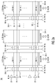
- FIG. 2 a shows ferroelectric memory array 300 with local plate line decoders 307 - 1 - 1 to 307 - m - j , according to one embodiment of the present invention.
- FIG. 2 b shows local plate line decoder 307 , which is suitable for implementing any of local plate line decoders 307 - 1 - 1 to 307 - m - j of FIG. 2 a.
- FIG. 2 c shows driver circuit 350 which provides signals “GPL” and “PRE” to be respectively placed on global plate lines (GPLs) 308 - 1 to 308 - m and pre-charge lines (PREs) 309 - 1 to 309 - m of ferroelectric memory array 300 of FIG. 2 a.
- GPLs global plate lines
- PREs pre-charge lines
- FIG. 3 a illustrates a read operation on a memory cell in ferroelectric memory array 300 under a first mode of operation, according to one embodiment of the present invention.
- FIG. 3 b illustrates a read operation on a memory cell in ferroelectric memory array 300 under a second mode of operation, according to one embodiment of the present invention.
- FIG. 4 a shows ferroelectric memory array 400 with 1T1C memory cells and local plate line decoders of the present invention, suitable for implementing any of memory array sections 302 - 1 , . . . , 302 - m in ferroelectric memory array 300 of FIG. 2 a.
- FIG. 4 b shows ferroelectric memory array 450 with 2T2C memory cells and local plate line decoders of the present invention, suitable for implementing any of memory array sections 302 - 1 , . . . , 302 - m in ferroelectric memory array 300 of FIG. 2 a.
- the present invention provides, in a ferroelectric memory array of a hierarchical plate line architecture, a local plate line decoder to drive a plate line segment.
- the present invention improves write speeds and provides better noise immunity, while providing an option to adjust the write energy that affects data retention.
- the memory may be operated in two or more modes. In one mode, the plate line may be pre-charged to one-half the memory array supply voltage (1 ⁇ 2 Vdda) and may be kept constant at Vdda/2 during read or write operation.
- FIG. 2 a shows ferroelectric memory array 300 with local plate line decoders 307 - 1 - 1 to 307 - m - j , according to one embodiment of the present invention.
- ferroelectric memory array 300 includes m memory array sections 302 - 1 , . . . , 302 - m , each having j rows of memory cells.
- Memory array sections 302 - 1 , . . . , 302 - m are served by j word lines 305 - 1 to 305 - j , driven respectively by word line drivers 401 - 1 to 401 - j .
- each memory array section is served by a local plate line segment (i.e., one of plate line segments 303 - 1 - 1 to 303 - 1 - j ).
- Plate line segments 303 - 1 - 1 to 303 - 1 - j are each driven by a corresponding one of local plate line decoders 307 - 1 - 1 to 307 - m - j .
- Memory array sections 302 - 1 , . . . , 302 - m each include a corresponding one of sense amplifier and input/output circuits 304 - 1 to 304 - m . These sense amplifier and input/output circuits may each be implemented using conventional circuitry such as those shown in FIG. 1 c .
- each of memory array sections 302 - 1 to 302 - m are served by k bit lines.
- Sense amplifier and input/output circuits 304 - 1 to 304 - m handle reading and writing in parallel signals on k/n of the k bit lines in its corresponding memory array section.
- Each memory cell of ferroelectric memory array 300 may be any ferroelectric memory cell, such as the 1T1C memory cell of FIG. 1 a , or the 2T2C memory cell of FIG. 1 b .
- memory array section 302 - 1 to 302 - m are each served by a global plate line (GPL) and a pre-charge control line (PRE), which are shown in FIG. 2 a as GPLs 308 - 1 to 308 - m and PREs 309 - 1 to 309 - m , respectively.
- GPL global plate line
- PREs 309 - 1 to 309 - m pre-charge control line
- FIG. 2 b shows local plate line decoder 307 , which is suitable for implementing any of local plate line decoders 307 - 1 - 1 to 307 - m - j of FIG. 2 a .
- local plate line decoder 307 receives the signals on a corresponding set of word line, GPL and PRE (i.e., word line 305 , GPL 308 and PRE 309 ) to provide a signal on a corresponding plate line segment (i.e., plate line segment 303 ).
- GPL and PRE i.e., word line 305 , GPL 308 and PRE 309
- Local plate line decoder 307 includes (i) MOS transistor 320 , which is controlled at its gate electrode by the signal on word line 305 , MOS transistor 320 connecting GPL 308 to plate line segment 303 , and (ii) MOS transistor 321 , which is controlled at its gate electrode by the signal on PRE 309 , MOS transistor 321 pre-charging plate line segment 303 to a pre-determined voltage VPL.
- Ferroelectric memory array 300 may be operated in one of two modes. In a first mode, to write into a memory cell, a higher voltage difference is imposed across each ferroelectric capacitor. In a second mode, to write into a memory cell, a lower voltage is imposed across each ferroelectric capacitor.
- the first mode provides a longer data retention time (e.g., 10 years or more). While the second mode provides a shorter data retention time (e.g., one year or less), it provides a lower-power operation and a faster random access time.
- FIG. 3 a illustrate a read operation of a memory cell in ferroelectric memory array 300 under the first mode of operation, according to one embodiment of the present invention.
- the signal on the PRE of each memory array section i.e., any of PREs 309 - 1 to 309 - m ; waveform 401 of FIG. 3 a
- V PL e.g. 0.75 to 1.0 volts, or half the memory array supply voltage V dda
- the signal on the PREs 309 - 1 to 309 - m are de-asserted, such that MOS transistor 321 of each local plate line decoder (e.g., any of local plate line decoders 307 - 1 - 1 to 307 - m - j ) is switched off.
- MOS transistor 321 of each local plate line decoder e.g., any of local plate line decoders 307 - 1 - 1 to 307 - m - j
- the signal on each GPL (waveform 402 ) is driven to a predetermined plate line read voltage (e.g., 1.5-2.0 volts, or the memory supply voltage V dda ), while the word line associated with the selected memory cell to be read (e.g., any of word lines 305 - 1 to 305 - j ) is driven to a predetermined read voltage (2.5-3.3 volts; waveform 408 ).
- the predetermined read voltage turns on MOS transistor 320 of the local plate line decoder associated with the selected memory cell to be read, such that the voltage on the associated plate line segment (waveform 403 ) follows the signal on the associated GPL.
- each bit line associated with each ferroelectric capacitor in the memory cell is coupled to a sense amplifier associated with the selected memory cell (i.e., a sense amplifier in the corresponding one of sense amplifier and input/output circuits 304 - 1 to 304 - m )
- FIG. 3 a is taken from an implementation of a 2T2C memory cell, which includes two ferroelectric capacitors storing complementary values.
- FIG. 3 a provides waveforms 404 (BL 0 ) and 405 (BLB 0 ), corresponding to the signals on the bit lines associated with the ferroelectric capacitors storing the “true” and “complement” values, when the memory cell stores the logic ‘0’ value.
- FIG. 3 a also provides waveforms 406 (BL 1 ) and 407 (BLB 1 ), corresponding to the signals on the bit lines associated with the ferroelectric capacitors storing the “true” and “complement” values, when the memory cell stores the logic ‘0’ value.
- waveforms 404 (BL 0 ) and 405 (BLB 0 ) are pulled by the sense amplifier to V dda and ground, respectively.
- waveforms 406 (BL 1 ) and 407 (BLB 1 ) are pulled by the sense amplifier to ground and V dda , respectively.
- a read operation on a ferroelectric memory cell programmed to the logic ‘1’ state may be destructive. Accordingly, a write-back operation is carried out to restore the logic state prior to completing the read operation.
- the signal on the associated GPL (waveform 402 ) is driven to ground so that the voltage on the associated plate line segment (waveform 403 ) follows in time also to ground voltage.
- V dda the voltage difference between the associated plate line segment and the “true” bit line in the memory cell storing the logic ‘1’ value is V dda , which effectuates an effective write-back of the logic value into the corresponding ferroelectric capacitor.
- the voltage difference between the associated plate line segment and the “complement” bit line is V dda , which effectuates an effective write back of the logic value to the corresponding ferroelectric capacitor).
- the write-back operation of FIG. 3 a stores sufficient “charge” into the ferroelectric capacitors for a long retention time (e.g., 10 years or more).
- programming voltage V pp equals the memory array supply voltage V dda .
- the read operation is complete. Accordingly, the signal on the associated word line (i.e., waveform 408 ) is de-asserted, such that MOS transistor 320 of the associated local plate line decoder is turned off. The voltages on the associated bit lines are also returned to quiescent voltage 1 ⁇ 2 V dda . Thereafter, as shown in FIG. 3 a , the signals on the PREs are asserted, such that the plate line segments are driven to quiescent voltage 1 ⁇ 2 V PL , which is also V dda in this example.
- V dda quiescent voltage 1 ⁇ 2 V PL
- FIG. 3 b illustrates a read operation of a memory cell in ferroelectric memory array 300 under a second mode of operation, according to one embodiment of the present invention.
- the signals on the PREs are set to a predetermined voltage that is sufficiently high (e.g., V dda or V PP ) that MOS transistor 321 of each local plate line decoder is constantly conducting. Therefore, in the example of FIG. 3 d , the signals on all plate line segments are maintained at 1 ⁇ 2 V dda (e.g., 0.75-1.0 volts) throughout the read operation.
- the signals on the GPLs are also set to 1 ⁇ 2 V dda throughout.
- FIG. 3 b provides waveforms 404 (BL 0 ) and 405 (BLB 0 ), corresponding to the signals on the bit lines associated with the ferroelectric capacitors storing the “true” and “complement” values, when the memory cell stores the logic ‘0’ value.
- FIG. 3 b provides waveforms 404 (BL 0 ) and 405 (BLB 0 ), corresponding to the signals on the bit lines associated with the ferroelectric capacitors storing the “true” and “complement” values, when the memory cell stores the logic ‘0’ value.
- waveforms 404 (BL 0 ) and 405 (BLB 0 ) are pulled by the sense amplifier to V dda and ground, respectively.
- waveforms 406 (BL 1 ) and 407 (BLB 1 ) are pulled by the sense amplifier to ground and V dda , respectively.
- the write operation for restoring the logic ‘1’ state also begins at time t 1 .
- the voltage difference between the associated plate line segment and the “true” bit line in the memory cell storing the logic ‘1’ value is 1 ⁇ 2 V dda , which also effectuates the write-back of the logic value into the corresponding ferroelectric capacitor.
- the voltage difference between the associated plate line segment and the “complement” bit line is 1 ⁇ 2 V dda , which also effectuates a write-hack of the logic value to the corresponding ferroelectric capacitor).
- the write-back operation of FIG. 3 b stores only sufficient “charge” into the ferroelectric capacitors for a lesser retention time (e.g., 1 year or less).
- the signal on the word line associated with the selected memory cell is de-asserted, as shown in FIG. 3 b , and the read operation is complete.
- FIG. 2 c shows driver circuit 350 which provides signals “GPL” and “PRE” respectively on GPLs 308 - 1 to 308 - m and PREs 309 - 1 to 309 - m of ferroelectric memory array 300 of FIG. 2 a .
- driver circuit 350 receives enable signal EN and control signal CA at terminals 361 and 362 , respectively, and provides output signals GPL and PRE at terminals 363 and 364 , respectively.
- Driver circuit 350 includes NAND gate 351 , NOR gate 352 , inverters 353 , 354 and 355 , PMOS transistor 356 and NMOS transistor 358 .
- signal EN is asserted prior to time t 0 and during the read operation to cause signal PRE to be de-asserted. While de-asserted, signal PRE turns off transistor 321 of local plate line decoder 307 , so that the associated plate line segment can be driven by the associated GPL at memory cells with asserted word line signals. At the same time, de-asserted signal EN turns off NMOS transistor 358 , to allow the voltage of signal GPL to be controlled by PMOS transistors 356 and 367 , respectively.
- control signal CA switches the voltage of signal GPL between V dda and ground through the actions of NAND gate 351 and NOR gate 352 , respectively, on PMOS transistor 356 and NMOS transistor 357 , as required, when the associated sense amplifier reads the logic state of the associated memory cell and during the write-back phase of the read value, respectively.
- signal EN is de-asserted, to assert signal PRE, to turn off PMOS transistor 356 and NMOS transistor 357 , and to turn on NMOS transistor 358 (which provides voltage 1 ⁇ 2 V dda on signal GPL).
- Asserted signal PRE turns on MOS transistor 321 of local plate line decoder 307 to bring the associated plate line segment to quiescent voltage 1 ⁇ 2 V dda .
- signal EN is asserted, so that PMOS transistor 356 and NMOS transistor 357 are turned off by NAND gate 351 and NOR gate 352 , respectively.
- signal EN causes signal PRE to be at logic value ‘1’ and turns on NMOS transistor 358 to provide voltage 1 ⁇ 2 V dda on signal GPL.
- signal PRE turns on MOS transistor 321 of local plate line decoder 307 , thereby driving its associated plate line segment to voltage V PL .
- FIG. 4 a shows ferroelectric memory array 400 with local plate line decoders of the present invention, suitable for implementing any of memory array sections 302 - 1 , . . . , 302 - m in ferroelectric memory array 300 of FIG. 2 a .
- Ferroelectric memory array 400 implements an “open bit line” sensing scheme, known to those of ordinary skill in the art.
- Each memory cell of ferroelectric memory array 400 is a 1T1C cell.
- FIG. 4 b shows ferroelectric memory array 450 with local plate line decoders of the present invention, suitable for implementing any of memory array sections 302 - 1 , . . . , 302 - m in ferroelectric memory array 300 of FIG. 2 a .
- Ferroelectric memory array 450 implements an “open bit line” sensing scheme, known to those of ordinary skill in the art.
- Each memory cell of ferroelectric memory array 450 is a 2T2C cell, storing a data value in “true” and “complement” forms.
Landscapes
- Engineering & Computer Science (AREA)
- Computer Hardware Design (AREA)
- Power Engineering (AREA)
- Microelectronics & Electronic Packaging (AREA)
- Dram (AREA)
- Semiconductor Memories (AREA)
Abstract
Description
Claims (12)
Priority Applications (2)
| Application Number | Priority Date | Filing Date | Title |
|---|---|---|---|
| US16/019,328 US10818334B2 (en) | 2018-06-26 | 2018-06-26 | Ferroelectric memory array with variable plate-line architecture |
| CN201910562601.4A CN110648701B (en) | 2018-06-26 | 2019-06-26 | Ferroelectric memory array with variable plate line architecture |
Applications Claiming Priority (1)
| Application Number | Priority Date | Filing Date | Title |
|---|---|---|---|
| US16/019,328 US10818334B2 (en) | 2018-06-26 | 2018-06-26 | Ferroelectric memory array with variable plate-line architecture |
Publications (2)
| Publication Number | Publication Date |
|---|---|
| US20190392884A1 US20190392884A1 (en) | 2019-12-26 |
| US10818334B2 true US10818334B2 (en) | 2020-10-27 |
Family
ID=68982068
Family Applications (1)
| Application Number | Title | Priority Date | Filing Date |
|---|---|---|---|
| US16/019,328 Active 2038-09-28 US10818334B2 (en) | 2018-06-26 | 2018-06-26 | Ferroelectric memory array with variable plate-line architecture |
Country Status (2)
| Country | Link |
|---|---|
| US (1) | US10818334B2 (en) |
| CN (1) | CN110648701B (en) |
Families Citing this family (3)
| Publication number | Priority date | Publication date | Assignee | Title |
|---|---|---|---|---|
| US11616068B1 (en) * | 2021-11-16 | 2023-03-28 | Micron Technology, Inc. | Deck selection layouts in a memory device |
| CN117133326A (en) * | 2022-05-18 | 2023-11-28 | 华为技术有限公司 | Ferroelectric memory and its control device, methods and equipment for improving its durability |
| CN118737221A (en) * | 2023-03-31 | 2024-10-01 | 华为技术有限公司 | Memory control method, device and electronic device |
Citations (5)
| Publication number | Priority date | Publication date | Assignee | Title |
|---|---|---|---|---|
| US20050226028A1 (en) * | 2004-04-05 | 2005-10-13 | Kazuhiko Takahashi | Ferroelectric memory |
| US20050286289A1 (en) * | 2004-06-24 | 2005-12-29 | Kenya Watanabe | Ferroelectric memory device |
| US20070081374A1 (en) * | 2005-10-06 | 2007-04-12 | Seiko Epson Corporation | Semiconductor memory device and electronic apparatus |
| US9972374B1 (en) * | 2016-10-30 | 2018-05-15 | AUCMOS Technologies USA, Inc. | Ferroelectric random access memory (FeRAM) array with segmented plate lines that are electrically-isolated from each other |
| US20190355404A1 (en) * | 2018-05-18 | 2019-11-21 | AUCMOS Technologies USA, Inc. | Ferroelectric Memory Array with Hierarchical Plate-Line Architecture |
Family Cites Families (7)
| Publication number | Priority date | Publication date | Assignee | Title |
|---|---|---|---|---|
| JP2002269969A (en) * | 2001-03-07 | 2002-09-20 | Nec Corp | Memory cell, non-volatile memory device, and its control method |
| JP3646791B2 (en) * | 2001-10-19 | 2005-05-11 | 沖電気工業株式会社 | Ferroelectric memory device and operation method thereof |
| KR100448921B1 (en) * | 2002-05-21 | 2004-09-16 | 삼성전자주식회사 | High-speed ferroelectric memory device and write methdo thereof |
| US6724645B1 (en) * | 2003-01-30 | 2004-04-20 | Agilent Technologies, Inc. | Method and apparatus for shortening read operations in destructive read memories |
| KR100597629B1 (en) * | 2003-12-22 | 2006-07-07 | 삼성전자주식회사 | Ferroelectric memory device and driving method thereof |
| JP4983062B2 (en) * | 2006-03-20 | 2012-07-25 | 富士通セミコンダクター株式会社 | Memory device |
| JP2016066394A (en) * | 2014-09-24 | 2016-04-28 | ラピスセミコンダクタ株式会社 | Ferroelectric memory |
-
2018
- 2018-06-26 US US16/019,328 patent/US10818334B2/en active Active
-
2019
- 2019-06-26 CN CN201910562601.4A patent/CN110648701B/en not_active Expired - Fee Related
Patent Citations (5)
| Publication number | Priority date | Publication date | Assignee | Title |
|---|---|---|---|---|
| US20050226028A1 (en) * | 2004-04-05 | 2005-10-13 | Kazuhiko Takahashi | Ferroelectric memory |
| US20050286289A1 (en) * | 2004-06-24 | 2005-12-29 | Kenya Watanabe | Ferroelectric memory device |
| US20070081374A1 (en) * | 2005-10-06 | 2007-04-12 | Seiko Epson Corporation | Semiconductor memory device and electronic apparatus |
| US9972374B1 (en) * | 2016-10-30 | 2018-05-15 | AUCMOS Technologies USA, Inc. | Ferroelectric random access memory (FeRAM) array with segmented plate lines that are electrically-isolated from each other |
| US20190355404A1 (en) * | 2018-05-18 | 2019-11-21 | AUCMOS Technologies USA, Inc. | Ferroelectric Memory Array with Hierarchical Plate-Line Architecture |
Also Published As
| Publication number | Publication date |
|---|---|
| CN110648701A (en) | 2020-01-03 |
| CN110648701B (en) | 2022-01-11 |
| US20190392884A1 (en) | 2019-12-26 |
Similar Documents
| Publication | Publication Date | Title |
|---|---|---|
| US5751626A (en) | Ferroelectric memory using ferroelectric reference cells | |
| US5917746A (en) | Cell plate structure for a ferroelectric memory | |
| US5677865A (en) | Ferroelectric memory using reference charge circuit | |
| US5999439A (en) | Ferroelectric memory using ferroelectric reference cells | |
| US5373463A (en) | Ferroelectric nonvolatile random access memory having drive line segments | |
| JP4801125B2 (en) | Nonvolatile ferroelectric memory device and multibit data writing method using the same | |
| US5574698A (en) | Ram row decode circuitry that utilizes a precharge circuit that is deactivated by a feedback from an activated word line driver | |
| US6711051B1 (en) | Static RAM architecture with bit line partitioning | |
| US4730279A (en) | Static semiconductor memory device | |
| US6778435B1 (en) | Memory architecture for TCCT-based memory cells | |
| JPH10340588A (en) | Nonvolatile memory device and writing method thereof | |
| US5881006A (en) | Semiconductor memory device | |
| US6320806B1 (en) | Input/output line precharge circuit and semiconductor memory device adopting the same | |
| US10818334B2 (en) | Ferroelectric memory array with variable plate-line architecture | |
| JP2001118380A (en) | Non-volatile ferroelectric memory device | |
| US4054865A (en) | Sense latch circuit for a bisectional memory array | |
| JP3980417B2 (en) | Integrated circuit memory | |
| EP0573046B1 (en) | Semiconductor memory device with single data line pair shared between memory cell arrays | |
| US6198653B1 (en) | Ferroelectric memory | |
| JP2004213830A (en) | Semiconductor storage device | |
| US6356476B1 (en) | Sensing amplifier of nonvolatile ferroelectric memory device | |
| US6940743B2 (en) | Semiconductor memory devices for outputting bit cell data without separate reference voltage generator and related methods of outputting bit cell data | |
| US7054181B2 (en) | Non-volatile ferroelectric cell array block having hierarchy transfer sensing architecture | |
| US10803918B2 (en) | Ferroelectric memory array with hierarchical plate-line architecture | |
| US6930902B2 (en) | Device for storing information and a method for partial write and restore |
Legal Events
| Date | Code | Title | Description |
|---|---|---|---|
| FEPP | Fee payment procedure |
Free format text: ENTITY STATUS SET TO UNDISCOUNTED (ORIGINAL EVENT CODE: BIG.); ENTITY STATUS OF PATENT OWNER: SMALL ENTITY |
|
| AS | Assignment |
Owner name: AUCMOS TECHNOLOGIES USA, INC., CALIFORNIA Free format text: ASSIGNMENT OF ASSIGNORS INTEREST;ASSIGNOR:ONG, ADRIAN E.;REEL/FRAME:046465/0579 Effective date: 20180627 |
|
| FEPP | Fee payment procedure |
Free format text: ENTITY STATUS SET TO SMALL (ORIGINAL EVENT CODE: SMAL); ENTITY STATUS OF PATENT OWNER: SMALL ENTITY |
|
| STPP | Information on status: patent application and granting procedure in general |
Free format text: NON FINAL ACTION MAILED |
|
| STPP | Information on status: patent application and granting procedure in general |
Free format text: RESPONSE TO NON-FINAL OFFICE ACTION ENTERED AND FORWARDED TO EXAMINER |
|
| STCF | Information on status: patent grant |
Free format text: PATENTED CASE |
|
| AS | Assignment |
Owner name: CHEN, YUNG-TIN, CALIFORNIA Free format text: ASSIGNMENT OF ASSIGNORS INTEREST;ASSIGNOR:AUCMOS TECHNOLOGIES USA, INC.;REEL/FRAME:067314/0379 Effective date: 20240503 |
|
| FEPP | Fee payment procedure |
Free format text: MAINTENANCE FEE REMINDER MAILED (ORIGINAL EVENT CODE: REM.); ENTITY STATUS OF PATENT OWNER: SMALL ENTITY |
|
| FEPP | Fee payment procedure |
Free format text: SURCHARGE FOR LATE PAYMENT, SMALL ENTITY (ORIGINAL EVENT CODE: M2554); ENTITY STATUS OF PATENT OWNER: SMALL ENTITY |
|
| MAFP | Maintenance fee payment |
Free format text: PAYMENT OF MAINTENANCE FEE, 4TH YR, SMALL ENTITY (ORIGINAL EVENT CODE: M2551); ENTITY STATUS OF PATENT OWNER: SMALL ENTITY Year of fee payment: 4 |
|
| AS | Assignment |
Owner name: PASCALINE SYSTEMS, INC., OHIO Free format text: ASSIGNMENT OF ASSIGNORS INTEREST;ASSIGNOR:AUCMOS TECHNOLOGIES, USA, INC.;REEL/FRAME:072908/0856 Effective date: 20250701 |