US10812111B2 - Semiconductor apparatus - Google Patents
Semiconductor apparatus Download PDFInfo
- Publication number
- US10812111B2 US10812111B2 US16/121,323 US201816121323A US10812111B2 US 10812111 B2 US10812111 B2 US 10812111B2 US 201816121323 A US201816121323 A US 201816121323A US 10812111 B2 US10812111 B2 US 10812111B2
- Authority
- US
- United States
- Prior art keywords
- error
- bits
- semiconductor apparatus
- ecc decoder
- selection unit
- Prior art date
- Legal status (The legal status is an assumption and is not a legal conclusion. Google has not performed a legal analysis and makes no representation as to the accuracy of the status listed.)
- Active
Links
Images


Classifications
-
- H—ELECTRICITY
- H03—ELECTRONIC CIRCUITRY
- H03M—CODING; DECODING; CODE CONVERSION IN GENERAL
- H03M13/00—Coding, decoding or code conversion, for error detection or error correction; Coding theory basic assumptions; Coding bounds; Error probability evaluation methods; Channel models; Simulation or testing of codes
- H03M13/29—Coding, decoding or code conversion, for error detection or error correction; Coding theory basic assumptions; Coding bounds; Error probability evaluation methods; Channel models; Simulation or testing of codes combining two or more codes or code structures, e.g. product codes, generalised product codes, concatenated codes, inner and outer codes
- H03M13/2906—Coding, decoding or code conversion, for error detection or error correction; Coding theory basic assumptions; Coding bounds; Error probability evaluation methods; Channel models; Simulation or testing of codes combining two or more codes or code structures, e.g. product codes, generalised product codes, concatenated codes, inner and outer codes using block codes
-
- G—PHYSICS
- G06—COMPUTING OR CALCULATING; COUNTING
- G06F—ELECTRIC DIGITAL DATA PROCESSING
- G06F11/00—Error detection; Error correction; Monitoring
- G06F11/07—Responding to the occurrence of a fault, e.g. fault tolerance
- G06F11/08—Error detection or correction by redundancy in data representation, e.g. by using checking codes
- G06F11/10—Adding special bits or symbols to the coded information, e.g. parity check, casting out 9's or 11's
- G06F11/1008—Adding special bits or symbols to the coded information, e.g. parity check, casting out 9's or 11's in individual solid state devices
- G06F11/1048—Adding special bits or symbols to the coded information, e.g. parity check, casting out 9's or 11's in individual solid state devices using arrangements adapted for a specific error detection or correction feature
-
- G—PHYSICS
- G06—COMPUTING OR CALCULATING; COUNTING
- G06F—ELECTRIC DIGITAL DATA PROCESSING
- G06F11/00—Error detection; Error correction; Monitoring
- G06F11/07—Responding to the occurrence of a fault, e.g. fault tolerance
- G06F11/08—Error detection or correction by redundancy in data representation, e.g. by using checking codes
- G06F11/10—Adding special bits or symbols to the coded information, e.g. parity check, casting out 9's or 11's
- G06F11/1004—Adding special bits or symbols to the coded information, e.g. parity check, casting out 9's or 11's to protect a block of data words, e.g. CRC or checksum
-
- G—PHYSICS
- G06—COMPUTING OR CALCULATING; COUNTING
- G06F—ELECTRIC DIGITAL DATA PROCESSING
- G06F11/00—Error detection; Error correction; Monitoring
- G06F11/07—Responding to the occurrence of a fault, e.g. fault tolerance
- G06F11/08—Error detection or correction by redundancy in data representation, e.g. by using checking codes
- G06F11/10—Adding special bits or symbols to the coded information, e.g. parity check, casting out 9's or 11's
- G06F11/1076—Parity data used in redundant arrays of independent storages, e.g. in RAID systems
-
- G—PHYSICS
- G06—COMPUTING OR CALCULATING; COUNTING
- G06F—ELECTRIC DIGITAL DATA PROCESSING
- G06F11/00—Error detection; Error correction; Monitoring
- G06F11/07—Responding to the occurrence of a fault, e.g. fault tolerance
- G06F11/16—Error detection or correction of the data by redundancy in hardware
- G06F11/18—Error detection or correction of the data by redundancy in hardware using passive fault-masking of the redundant circuits
- G06F11/183—Error detection or correction of the data by redundancy in hardware using passive fault-masking of the redundant circuits by voting, the voting not being performed by the redundant components
-
- H—ELECTRICITY
- H03—ELECTRONIC CIRCUITRY
- H03M—CODING; DECODING; CODE CONVERSION IN GENERAL
- H03M13/00—Coding, decoding or code conversion, for error detection or error correction; Coding theory basic assumptions; Coding bounds; Error probability evaluation methods; Channel models; Simulation or testing of codes
- H03M13/03—Error detection or forward error correction by redundancy in data representation, i.e. code words containing more digits than the source words
- H03M13/05—Error detection or forward error correction by redundancy in data representation, i.e. code words containing more digits than the source words using block codes, i.e. a predetermined number of check bits joined to a predetermined number of information bits
- H03M13/13—Linear codes
- H03M13/19—Single error correction without using particular properties of the cyclic codes, e.g. Hamming codes, extended or generalised Hamming codes
Definitions
- Embodiments described herein relate generally to a semiconductor apparatus.
- a semiconductor apparatus provided with an SRAM includes an ECC encoder and an ECC decoder to correct data errors in the SRAM, whereby functional safety is enhanced.
- ECC encoder and an ECC decoder to correct data errors in the SRAM, whereby functional safety is enhanced.
- ECC decoder to correct data errors in the SRAM, whereby functional safety is enhanced.
- an error of one bit can be corrected while an error of two bits or more can be detected.
- FIG. 1 is a block diagram illustrating a configuration of a semiconductor apparatus according to a first embodiment
- FIG. 2 is a block diagram illustrating a configuration of a semiconductor apparatus according to a modification of the first embodiment
- FIG. 3 is a block diagram illustrating a configuration of a semiconductor apparatus according to a second embodiment
- FIG. 4 is a block diagram illustrating a configuration of a semiconductor apparatus according to a modification of the second embodiment
- FIG. 5 is a block diagram illustrating a configuration of a semiconductor apparatus according to a third embodiment.
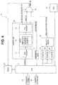
- FIG. 6 is a block diagram illustrating a configuration of a semiconductor apparatus according to a modification of the third embodiment.
- a semiconductor apparatus includes a storage unit, an ECC decoder, and a selection unit.
- the storage unit stores data.
- the ECC decoder can detect and correct an error of a predetermined number of bits in data outputted from the storage unit, and can detect an error equal to or larger than bits larger than the predetermined number of bits in the data.
- the selection unit selects and outputs one of the data outputted from the ECC decoder and a preset fixed value, in accordance with a detection signal indicating whether or not the error equal to or larger than the bits larger than the predetermined number of bits is detected by the ECC decoder.
- FIG. 1 is a block diagram illustrating the configuration of the semiconductor apparatus according to the first embodiment.
- a semiconductor apparatus 1 of the first embodiment includes an ECC encoder 11 , an SRAM 12 , an ECC decoder 13 , a register 14 a , a multiplexer 15 , a CPU 16 , and an error information register 17 .
- the SRAM 12 includes a data storage unit 12 a and an ECC storage unit 12 b.
- Data stored in the SRAM 12 is inputted to the ECC encoder 11 .
- the ECC encoder 11 encodes the inputted data, and outputs the data and an ECC (an error-correction code) to the SRAM 12 .
- the SRAM 12 as the storage unit stores the data from the ECC encoder 11 in the data storage unit 12 a , and stores the ECC in the ECC storage unit 12 b .
- the SRAM 12 is used as the storage unit.
- the storage unit is not limited to the SRAM 12 , but may be a ROM or a NAND flash memory, for example.
- the ECC decoder 13 can detect and correct an error of one bit, and can detect an error of two bits or more in the data.
- the ECC decoder 13 decodes the data and the ECC inputted from the SRAM 12 .
- the ECC decoder 13 outputs the data from the SRAM 12 to the multiplexer 15 .
- the ECC decoder 13 when no error is included in the data from the SRAM 12 , the ECC decoder 13 outputs the data including no error to the multiplexer 15 , and when an error of one bit is included in the data from the SRAM 12 , the ECC decoder 13 outputs, to the multiplexer 15 , resultant data in which the error of one bit has been corrected.
- the ECC decoder 13 cannot correct the error. Accordingly, the ECC decoder 13 outputs the data including the error of two bits or more to the multiplexer 15 .
- the ECC decoder 13 when an error of one bit or more is included in the data from the SRAM 12 , the ECC decoder 13 outputs error information to the error information register 17 .
- the error information held in the error information register 17 can be read out by the CPU 16 , for example.
- the ECC decoder 13 outputs a detection signal regarding an error of two bits or more to the multiplexer 15 .
- the ECC decoder 13 outputs a detection signal “O” to the multiplexer 15 when no error of two bits or more is included in the data from the SRAM 12
- the ECC decoder 13 outputs a detection signal “1” to the multiplexer 15 when an error of two bits or more is included in the data from the SRAM 12 .
- a fixed value (a preset fixed value) for maintaining functional safety of the semiconductor apparatus 1 is stored in the register 14 a .
- the fixed value stored in the register 14 a is inputted to the multiplexer 15 .
- the multiplexer 15 as the selection unit selects one of the data from the ECC decoder 13 and the fixed value from the register 14 a in accordance with the detection signal regarding an error of two bits or more, and outputs the selected one to the CPU 16 . More specifically, when no error of two bits or more is included in the data from the SRAM 12 and the detection signal “0” is inputted to the multiplexer 15 , the multiplexer 15 outputs the data from the ECC decoder 13 to the CPU 16 . When an error of two bits or more is included in the data from the SRAM 12 and the detection signal “1” is inputted to the multiplexer 15 , the multiplexer 15 outputs the fixed value from the register 14 a to the CPU 16 .
- the semiconductor apparatus 1 of the present embodiment includes the ECC decoder 13 capable of detecting and correcting an error of one bit, and detecting an error of two bits or more in the data
- the semiconductor apparatus 1 is not limited to this configuration.
- the ECC decoder 13 may be configured to be capable of detecting and correcting an error of two bits in the data, and detecting an error of three bits or more.
- the ECC decoder 13 may also be configured to be capable of detecting and correcting an error of three bits in the data, and detecting an error of four bits or more.
- the ECC decoder 13 is configured to be capable of detecting and correcting an error of a predetermined number of bits in the data outputted from the SRAM 12 , and detecting an error equal to or larger than bits larger than the predetermined number of bits.
- the multiplexer 15 which serves as the selection unit, selects and outputs to the CPU 16 , one of the data from the ECC decoder 13 and the fixed value from the register 14 a in accordance with the detection signal indicating whether or not the error equal to or larger than the bits larger than the predetermined number of bits is detected by the ECC decoder 13 .
- the semiconductor apparatus 1 is enabled to maintain safety even when the data from the SRAM 12 has an error equal to or larger than bits larger than the predetermined number of bits.
- FIG. 2 is a block diagram illustrating a configuration of a semiconductor apparatus according to the modification of the first embodiment.
- components identical to the components in FIG. 1 are denoted by the same reference numerals, and an explanation of the components is omitted.
- a semiconductor apparatus 1 a is formed by adding a register 14 b , a register 14 c , and a majority circuit 18 to the semiconductor apparatus 1 in FIG. 1 .
- the semiconductor apparatus 1 a is obtained by multiplexing (triplexing, in the case in FIG. 2 ) the register 14 a of the semiconductor apparatus 1 in FIG. 1 .
- the register 14 a of the semiconductor apparatus 1 in FIG. 1 is triplexed.
- the register is not limited to the configuration, but may be quadruplexed.
- Fixed values for securing the safe state of the semiconductor apparatus 1 a are stored in the registers 14 a , 14 b , 14 c .
- the fixed values stored in the registers 14 a , 14 b , 14 c are inputted to the majority circuit 18 .
- the majority circuit 18 determines a majority of the fixed values inputted from the registers 14 a , 14 b , 14 c by making a majority decision, and outputs the fixed value determined by the majority decision to the multiplexer 15 .
- the remaining components are identical to the components of the first embodiment.
- the fixed value held in the register 14 a may be replaced by an unintended fixed value due to a malfunction or noise, etc., in the register 14 a .
- the functional safety of the semiconductor apparatus 1 may not be maintained.
- the fixed values for securing the safe state of the semiconductor apparatus 1 a are inputted from the registers 14 b , 14 c to the majority circuit 18 .
- a fixed value for securing the safe state of the semiconductor apparatus 1 a is selected through a majority decision made by the majority circuit 18 , and is outputted to the multiplexer 15 .
- the functional safety of the semiconductor apparatus 1 a of the modification can be more reliably maintained than the semiconductor apparatus 1 of the first embodiment.
- FIG. 3 is a block diagram illustrating a configuration of a semiconductor apparatus according to the second embodiment.
- components identical to the components in FIG. 1 are denoted by the same reference numerals, and an explanation of the components is omitted.
- a semiconductor apparatus 1 b is formed by adding a bus 21 , a memory unit 22 that holds a vector address, and an interruption controller 23 to the semiconductor apparatus 1 in FIG. 1 .
- the interruption controller 23 includes an interruption selection unit 24 .
- the memory unit 22 that holds a vector address includes the ECC encoder 11 , the SRAM 12 , and the ECC decoder 13 .
- the vector address is inputted to the ECC encoder 11 via the bus 21 .
- the ECC encoder 11 encodes the inputted vector address, and outputs the vector address and an ECC to the SRAM 12 . Accordingly, a plurality of vector addresses are stored in the SRAM 12 .
- a plurality of interrupt factors 25 a , 25 b , . . . are inputted to the interruption selection unit 24 of the interruption controller 23 .
- the interruption selection unit 24 outputs, to the CPU 16 , an interrupt signal so as to cause the CPU 16 to execute an interruption process having the highest priority among the interrupt factors 25 a , 25 b , . . . . Further, the interruption selection unit 24 outputs, to the memory unit 22 , an address selection signal to select a vector address for allowing execution of the interrupt process having the highest priority. As a result, the selected vector address and the ECC are inputted from the SRAM 12 to the ECC decoder 13 .
- the ECC decoder 13 decodes the vector address and the ECC inputted from the SRAM 12 .
- the ECC decoder 13 When no error is included in the vector address from the SRAM 12 , the ECC decoder 13 outputs the vector address including no error to the multiplexer 15 , and when an error of one bit is included in the vector address from the SRAM 12 , the ECC decoder 13 outputs, to the multiplexer 15 , a resultant vector address in which the error of one bit has been corrected.
- the ECC decoder 13 cannot correct the error. Accordingly, the ECC decoder 13 outputs the vector address including the error of two bits or more to the multiplexer 15 .
- the ECC decoder 13 outputs a detection signal regarding an error of two bits or more to the multiplexer 15 . For example, when no error of two bits or more is included in the vector address from the SRAM 12 , the ECC decoder 13 outputs a detection signal “0” to the multiplexer 15 , and when an error of two bits or more is included in the vector address from the SRAM 12 , the ECC decoder 13 outputs a detection signal “I” to the multiplexer 15 .
- the register 14 a stores the vector address for allowing execution of a safe process (a vector address for allowing execution of a preset process), which is inputted via the bus 21 to the register 14 a .
- the vector address for allowing execution of a safe process stored in the register 14 a is inputted to the multiplexer 15 .
- the multiplexer 15 selects one of the vector address from the ECC decoder 13 and the vector address from the register 14 a for allowing execution of a safe process, in accordance with the detection signal regarding an error of two bits or more, and outputs the selected vector address to the CPU 16 . More specifically, when no error of two bits or more is included in the vector address from the SRAM 12 and a detection signal “0” is inputted to the multiplexer 15 , the multiplexer 15 outputs the vector address from the ECC decoder 13 to the CPU 16 .
- the multiplexer 15 When an error of two bits or more is included in the vector address from the SRAM 12 and a detection signal “1” is inputted to the multiplexer 15 , the multiplexer 15 outputs, to the CPU 16 , the vector address from the register 14 a for allowing execution of a safe process.
- the vector address for allowing execution of a safe process is outputted to the CPU 16 .
- the semiconductor apparatus 1 b of the present embodiment is configured such that, when an error of two bits or more is included in the vector address stored in the SRAM 12 , the vector address for allowing execution of a safe process, held in the register 14 a , is selected by the multiplexer 15 and is inputted to the CPU 16 .
- FIG. 4 is a block diagram illustrating a configuration of a semiconductor apparatus according to the modification of the second embodiment.
- components identical to the components in FIG. 3 are denoted by the same reference numerals, and an explanation of the components is omitted.
- a semiconductor apparatus 1 c is formed by adding the register 14 b , the register 14 c , and the majority circuit 18 to the semiconductor apparatus 1 b in FIG. 3 .
- the semiconductor apparatus 1 c is obtained by multiplexing (triplexing in the case in FIG. 4 ) the register 14 a of the semiconductor apparatus 1 b in FIG. 3 .
- the register 14 a of the semiconductor apparatus 1 b in FIG. 3 is triplexed.
- the register is not limited to the configuration, but may be quadruplexed.
- Vector addresses for allowing execution of a safe process inputted to the registers 14 a , 14 b , 14 c via the bus 21 are stored in the registers 14 a , 14 b , 14 c .
- the vector addresses for allowing execution of a safe process stored in the registers 14 a , 14 b , 14 c are inputted to the majority circuit 18 .
- the majority circuit 18 determines a majority of the vector addresses inputted from the registers 14 a , 14 b , 14 c by making a majority decision, and outputs the vector address determined by the majority decision to the multiplexer 15 .
- the remaining components are identical to the components of the second embodiment.
- the vector address for allowing execution of a safe process held in the register 14 a may be replaced by an unintended vector address due to a malfunction or noise, etc., in the register 14 a .
- a runaway of the CPU 16 for example, may be caused, and the functional safety of the semiconductor apparatus 1 b may not be maintained.
- the semiconductor apparatus 1 c of the modification is configured such that, when the vector address for allowing execution of a safe process held in the register 14 a is replaced by an unintended vector address, vector addresses for allowing execution of a safe process are inputted from the registers 14 b , 14 c to the majority circuit 18 .
- a vector address for allowing execution of a safe process is selected through a majority decision made by the majority circuit 18 , and is outputted to the multiplexer 15 .
- the functional safety of the semiconductor apparatus 1 c of the modification can be more reliably maintained than the semiconductor apparatus 1 b of the second embodiment.
- DMAC DMA controller
- FIG. 5 is a block diagram illustrating a configuration of a semiconductor apparatus according to the third embodiment.
- components identical to the components in FIGS. 1 and 3 are denoted by the same reference numerals, and an explanation of the components is omitted.
- a semiconductor apparatus 1 d is formed by adding the bus 21 , a DMAC 31 , a memory unit 32 that holds an instruction code (a command sequence) for the DMAC 31 , a transfer source device 33 , and a transfer destination device 34 to the semiconductor apparatus 1 in FIG. 1 .
- the memory unit 32 that holds the instruction code includes the ECC encoder 11 , the SRAM 12 , and the ECC decoder 13 .
- the ECC encoder 11 encodes the instruction code inputted to the ECC encoder 11 via the bus 21 , and outputs the instruction code and an ECC to the SRAM 12 . Accordingly, a plurality of instruction codes for the DMAC 31 and ECCs are stored in the SRAM 12 .
- the ECC decoder 13 decodes an instruction code and an ECC read from the SRAM 12 .
- the ECC decoder 13 outputs the instruction code including no error to the multiplexer 15 .
- the ECC decoder 13 outputs, to the multiplexer 15 , a resultant instruction code in which the error of one bit has been corrected.
- the ECC decoder 13 cannot correct the error. Accordingly, the ECC decoder 13 outputs the instruction code including the error of two bits or more to the multiplexer 15 .
- the ECC decoder 13 outputs a detection signal regarding an error of two bits or more to the multiplexer 15 . For example, when no error of two bits or more is included in the instruction code from the SRAM 12 , the ECC decoder 13 outputs a detection signal “0” to the multiplexer 15 , and when an error of two bits or more is included in the instruction code from the SRAM 12 , the ECC decoder 13 outputs a detection signal “1” to the multiplexer 15 .
- the register 14 a stores the instruction code for allowing execution of a safe process (instruction code for execution of a preset process), inputted to the register 14 a via the bus 21 .
- the instruction code for allowing execution of a safe process stored in the register 14 a is inputted to the multiplexer 15 .
- the multiplexer 15 selects one of the instruction code from the ECC decoder 13 and the instruction code for allowing execution of a safe process from the register 14 a in accordance with the detection signal regarding an error of two bits or more, and outputs the selected instruction code to the CPU 16 . More specifically, when no error of two bits or more is included in the instruction code from the SRAM 12 and a detection signal “0” is inputted to the multiplexer 15 , the multiplexer 15 outputs the instruction code from the ECC decoder 13 to the CPU 16 .
- the multiplexer 15 When an error of two bits or more is included in the instruction code from the SRAM 12 and a detection signal “1” is inputted to the multiplexer 15 , the multiplexer 15 outputs the instruction code from the register 14 a for allowing execution of a safe process to the CPU 16 .
- the DMAC 31 can perform control to cause direct transfer of data from the transfer source device 33 to the transfer destination device 34 via the bus 21 .
- the instruction code for allowing execution of a safe process stored in the register 14 a is selected by the multiplexer 15 , and is inputted to the DMAC 31 .
- the DMAC 31 executes the inputted instruction code for allowing execution of a safe process, so that erroneous transfer of data can be prevented.
- FIG. 6 is a block diagram illustrating a configuration of a semiconductor apparatus according to the modification of the third embodiment.
- components identical to the components in FIG. 5 are denoted by the same reference numerals, and an explanation of the components is omitted.
- a semiconductor apparatus 1 e is formed by adding the register 14 b , the register 14 c , and the majority circuit 18 to the semiconductor apparatus 1 d in FIG. 5 .
- the semiconductor apparatus 1 e is obtained by multiplexing (triplexing in the case in FIG. 6 ) the register 14 a of the semiconductor apparatus 1 d in FIG. 5 .
- the register 14 a of the semiconductor apparatus 1 d in FIG. 5 is triplexed.
- the register is not limited to the configuration, but may be quadruplexed.
- Instruction codes for allowing execution of a safe process are inputted to the registers 14 a , 14 b , 14 c via the bus 21 , and are stored in the registers 14 a . 14 b , 14 c .
- the instruction codes for allowing execution of a safe process stored in the registers 14 a , 14 b , 14 c are inputted to the majority circuit 18 .
- the majority circuit 18 determines a majority of the instruction codes inputted from the registers 14 a , 14 b , 14 c by making a majority decision, and outputs the instruction code determined by the majority decision to the multiplexer 15 .
- the remaining components are identical to the components of the third embodiment.
- the instruction code for allowing execution of a safe process held in the register 14 a may be replaced by an unintended instruction code due to a malfunction or noise, etc., in the register 14 a .
- the instruction code for allowing execution of a safe process held in the register 14 a is replaced by an unintended instruction code, erroneous transfer of data, for example, may be caused by the DMAC 31 , and the functional safety of the semiconductor apparatus 1 d may not be maintained.
- the semiconductor apparatus 1 c of the modification is configured such that, when the instruction code for allowing execution of a safe process held in the register 14 a is replaced by an unintended instruction code, instruction codes for allowing execution of a safe process are inputted from the registers 14 b , 14 c to the majority circuit 18 .
- An instruction code for allowing execution of a safe process is selected through a majority decision made by the majority circuit 18 , and is outputted to the multiplexer 15 .
- the functional safety of the semiconductor apparatus 1 e of the modification can be more reliably maintained than the semiconductor apparatus 1 d of the third embodiment.
Landscapes
- Engineering & Computer Science (AREA)
- Theoretical Computer Science (AREA)
- Physics & Mathematics (AREA)
- General Engineering & Computer Science (AREA)
- Quality & Reliability (AREA)
- General Physics & Mathematics (AREA)
- Probability & Statistics with Applications (AREA)
- Computer Security & Cryptography (AREA)
- Hardware Redundancy (AREA)
- Detection And Correction Of Errors (AREA)
- Logic Circuits (AREA)
Abstract
Description
Claims (16)
Applications Claiming Priority (2)
| Application Number | Priority Date | Filing Date | Title |
|---|---|---|---|
| JP2018-051138 | 2018-03-19 | ||
| JP2018051138A JP2019164472A (en) | 2018-03-19 | 2018-03-19 | Semiconductor device |
Publications (2)
| Publication Number | Publication Date |
|---|---|
| US20190288709A1 US20190288709A1 (en) | 2019-09-19 |
| US10812111B2 true US10812111B2 (en) | 2020-10-20 |
Family
ID=67904239
Family Applications (1)
| Application Number | Title | Priority Date | Filing Date |
|---|---|---|---|
| US16/121,323 Active US10812111B2 (en) | 2018-03-19 | 2018-09-04 | Semiconductor apparatus |
Country Status (3)
| Country | Link |
|---|---|
| US (1) | US10812111B2 (en) |
| JP (1) | JP2019164472A (en) |
| CN (1) | CN110287057A (en) |
Families Citing this family (2)
| Publication number | Priority date | Publication date | Assignee | Title |
|---|---|---|---|---|
| JP7383589B2 (en) * | 2020-09-23 | 2023-11-20 | 株式会社東芝 | information processing equipment |
| KR20230046740A (en) * | 2021-09-30 | 2023-04-06 | 에스케이하이닉스 주식회사 | Memory and operation method of memory |
Citations (14)
| Publication number | Priority date | Publication date | Assignee | Title |
|---|---|---|---|---|
| US5215537A (en) | 1990-09-13 | 1993-06-01 | Lynn Lawrence A | Septum for a blunt cannula |
| US5608891A (en) * | 1992-10-06 | 1997-03-04 | Mitsubishi Denki Kabushiki Kaisha | Recording system having a redundant array of storage devices and having read and write circuits with memory buffers |
| JPH09282237A (en) | 1996-04-19 | 1997-10-31 | Fujitsu General Ltd | Storage device using EEPROM |
| JP2005149183A (en) | 2003-11-17 | 2005-06-09 | Bosch Automotive Systems Corp | Error failsafe processing method of semiconductor storage element |
| US20060080580A1 (en) * | 2004-10-11 | 2006-04-13 | Conti Gregory R P | Method and system for detecting a security violation using an error correction code |
| JP2006171952A (en) | 2004-12-14 | 2006-06-29 | Renesas Technology Corp | Semiconductor integrated circuit device |
| JP2006285976A (en) | 2005-03-10 | 2006-10-19 | Matsushita Electric Ind Co Ltd | Nonvolatile storage system, nonvolatile storage device, data reading method, and reading program |
| US20070124653A1 (en) * | 2004-10-11 | 2007-05-31 | Texas Instruments Incorporated | Method and System for Detecting a Security Violation Using an Error Correction Code |
| JP2008011078A (en) | 2006-06-28 | 2008-01-17 | Samsung Electronics Co Ltd | Information encoding apparatus, information decoding apparatus, information encoding method, and information decoding method |
| US7424648B2 (en) | 2005-03-10 | 2008-09-09 | Matsushita Electric Industrial Co., Ltd. | Nonvolatile memory system, nonvolatile memory device, data read method, and data read program |
| US20100169546A1 (en) * | 2006-08-15 | 2010-07-01 | Koninklijke Philips Electronics N.V. | Flash memory access circuit |
| US20140229793A1 (en) * | 2013-02-11 | 2014-08-14 | Arm Limited | Apparatus and method for controlling access to a memory device |
| JP5905588B2 (en) | 2012-09-10 | 2016-04-20 | ルネサスエレクトロニクス株式会社 | Semiconductor device and battery voltage monitoring device |
| US20170242823A1 (en) | 2016-02-19 | 2017-08-24 | Denso Corporation | Microcontroller and electronic control unit |
Family Cites Families (7)
| Publication number | Priority date | Publication date | Assignee | Title |
|---|---|---|---|---|
| JPH05143365A (en) * | 1991-11-21 | 1993-06-11 | Nec Corp | Interruption table expansion/protection system |
| JP3080552B2 (en) * | 1994-12-26 | 2000-08-28 | 三菱電機株式会社 | Memory device for multi-computer system |
| JP2007257791A (en) * | 2006-03-24 | 2007-10-04 | Fujitsu Ltd | Semiconductor memory device |
| JP5158030B2 (en) * | 2008-09-29 | 2013-03-06 | 株式会社デンソー | Electronic control device for vehicle |
| JP5813450B2 (en) * | 2011-10-17 | 2015-11-17 | 日立オートモティブシステムズ株式会社 | Electronic control unit |
| JP5915490B2 (en) * | 2012-10-05 | 2016-05-11 | 株式会社デンソー | Electronic control unit |
| KR102324769B1 (en) * | 2015-06-29 | 2021-11-10 | 삼성전자주식회사 | Error correction circuit, semiconductor memory device and memory system including the same |
-
2018
- 2018-03-19 JP JP2018051138A patent/JP2019164472A/en active Pending
- 2018-08-10 CN CN201810906878.XA patent/CN110287057A/en active Pending
- 2018-09-04 US US16/121,323 patent/US10812111B2/en active Active
Patent Citations (17)
| Publication number | Priority date | Publication date | Assignee | Title |
|---|---|---|---|---|
| US5215537A (en) | 1990-09-13 | 1993-06-01 | Lynn Lawrence A | Septum for a blunt cannula |
| US5608891A (en) * | 1992-10-06 | 1997-03-04 | Mitsubishi Denki Kabushiki Kaisha | Recording system having a redundant array of storage devices and having read and write circuits with memory buffers |
| JPH09282237A (en) | 1996-04-19 | 1997-10-31 | Fujitsu General Ltd | Storage device using EEPROM |
| JP2005149183A (en) | 2003-11-17 | 2005-06-09 | Bosch Automotive Systems Corp | Error failsafe processing method of semiconductor storage element |
| US20070124653A1 (en) * | 2004-10-11 | 2007-05-31 | Texas Instruments Incorporated | Method and System for Detecting a Security Violation Using an Error Correction Code |
| US20060080580A1 (en) * | 2004-10-11 | 2006-04-13 | Conti Gregory R P | Method and system for detecting a security violation using an error correction code |
| JP2006171952A (en) | 2004-12-14 | 2006-06-29 | Renesas Technology Corp | Semiconductor integrated circuit device |
| US20060156075A1 (en) | 2004-12-14 | 2006-07-13 | Renesas Technology Corp. | Semiconductor integrated circuit |
| JP2006285976A (en) | 2005-03-10 | 2006-10-19 | Matsushita Electric Ind Co Ltd | Nonvolatile storage system, nonvolatile storage device, data reading method, and reading program |
| US7424648B2 (en) | 2005-03-10 | 2008-09-09 | Matsushita Electric Industrial Co., Ltd. | Nonvolatile memory system, nonvolatile memory device, data read method, and data read program |
| JP2008011078A (en) | 2006-06-28 | 2008-01-17 | Samsung Electronics Co Ltd | Information encoding apparatus, information decoding apparatus, information encoding method, and information decoding method |
| US20100169546A1 (en) * | 2006-08-15 | 2010-07-01 | Koninklijke Philips Electronics N.V. | Flash memory access circuit |
| JP5905588B2 (en) | 2012-09-10 | 2016-04-20 | ルネサスエレクトロニクス株式会社 | Semiconductor device and battery voltage monitoring device |
| US9564765B2 (en) | 2012-09-10 | 2017-02-07 | Renesas Electronics Corporation | Semiconductor device and battery voltage monitoring device |
| US20140229793A1 (en) * | 2013-02-11 | 2014-08-14 | Arm Limited | Apparatus and method for controlling access to a memory device |
| US20170242823A1 (en) | 2016-02-19 | 2017-08-24 | Denso Corporation | Microcontroller and electronic control unit |
| JP2017146897A (en) | 2016-02-19 | 2017-08-24 | 株式会社デンソー | Microcontroller and electronic control device |
Non-Patent Citations (1)
| Title |
|---|
| Chen, P-Y., et al., "An Enhanced EDAC Methodology for Low Power PSRAM", 2006 IEEE International Test Conference, Conference Location: Santa Clara, CA, USA, Date of Conference: Oct. 22-27, 2006, pp. 1-10. (Year: 2006). * |
Also Published As
| Publication number | Publication date |
|---|---|
| JP2019164472A (en) | 2019-09-26 |
| US20190288709A1 (en) | 2019-09-19 |
| CN110287057A (en) | 2019-09-27 |
Similar Documents
| Publication | Publication Date | Title |
|---|---|---|
| US9037941B2 (en) | Systems and methods for error checking and correcting for memory module | |
| US9811429B2 (en) | Microcontroller utilizing redundant address decoders and electronic control device using the same | |
| KR102828487B1 (en) | Memory module, memory system including the same and error correcting method thereof | |
| CN107430540B (en) | Runtime ECC Error Injection Scheme for Hardware Verification | |
| US9164831B2 (en) | Memory controller, semiconductor storage device, and decoding method | |
| KR100921263B1 (en) | Semiconductor storage device and decord method | |
| KR20160027059A (en) | Use of error correction pointers to handle errors in memory | |
| US10795763B2 (en) | Memory system and error correcting method thereof | |
| KR20160084790A (en) | Information processing apparatus and system providing plurality of levels of error correction, and operating method thereof | |
| US10802912B2 (en) | Semiconductor memory device and memory system having the same | |
| US10824507B2 (en) | Semiconductor memory device, controller, and memory system | |
| KR20170035795A (en) | Method and associated decoding circuit for decoding an error correction code | |
| CN109947674B (en) | Data processing device and data processing method | |
| US10812111B2 (en) | Semiconductor apparatus | |
| US10514980B2 (en) | Encoding method and memory storage apparatus using the same | |
| US10340955B2 (en) | Data processing circuit | |
| JP6332134B2 (en) | Memory diagnostic circuit | |
| JP2012003569A (en) | Memory controller, flash memory system including memory controller, and method of controlling flash memory | |
| US9092354B2 (en) | Storage device, CRC generation device, and CRC generation method | |
| JP7182373B2 (en) | Semiconductor integrated circuit, memory device and error correction method | |
| KR102788902B1 (en) | Memory system | |
| US10268547B2 (en) | Memory protection device and method | |
| US20140245101A1 (en) | Semiconductor memory | |
| JP2013069377A (en) | Decoding method, decoding device and storage device | |
| JP2013201503A (en) | Chien search circuit, decoder, storage device and chien search method |
Legal Events
| Date | Code | Title | Description |
|---|---|---|---|
| FEPP | Fee payment procedure |
Free format text: ENTITY STATUS SET TO UNDISCOUNTED (ORIGINAL EVENT CODE: BIG.); ENTITY STATUS OF PATENT OWNER: LARGE ENTITY |
|
| AS | Assignment |
Owner name: TOSHIBA ELECTRONIC DEVICES & STORAGE CORPORATION, Free format text: ASSIGNMENT OF ASSIGNORS INTEREST;ASSIGNOR:LIN, KEISYUN;REEL/FRAME:047421/0446 Effective date: 20180926 Owner name: KABUSHIKI KAISHA TOSHIBA, JAPAN Free format text: ASSIGNMENT OF ASSIGNORS INTEREST;ASSIGNOR:LIN, KEISYUN;REEL/FRAME:047421/0446 Effective date: 20180926 Owner name: TOSHIBA ELECTRONIC DEVICES & STORAGE CORPORATION, JAPAN Free format text: ASSIGNMENT OF ASSIGNORS INTEREST;ASSIGNOR:LIN, KEISYUN;REEL/FRAME:047421/0446 Effective date: 20180926 |
|
| STPP | Information on status: patent application and granting procedure in general |
Free format text: NON FINAL ACTION MAILED |
|
| STPP | Information on status: patent application and granting procedure in general |
Free format text: RESPONSE TO NON-FINAL OFFICE ACTION ENTERED AND FORWARDED TO EXAMINER |
|
| STPP | Information on status: patent application and granting procedure in general |
Free format text: FINAL REJECTION MAILED |
|
| STPP | Information on status: patent application and granting procedure in general |
Free format text: ADVISORY ACTION MAILED |
|
| STPP | Information on status: patent application and granting procedure in general |
Free format text: DOCKETED NEW CASE - READY FOR EXAMINATION |
|
| STPP | Information on status: patent application and granting procedure in general |
Free format text: NOTICE OF ALLOWANCE MAILED -- APPLICATION RECEIVED IN OFFICE OF PUBLICATIONS |
|
| STCF | Information on status: patent grant |
Free format text: PATENTED CASE |
|
| MAFP | Maintenance fee payment |
Free format text: PAYMENT OF MAINTENANCE FEE, 4TH YEAR, LARGE ENTITY (ORIGINAL EVENT CODE: M1551); ENTITY STATUS OF PATENT OWNER: LARGE ENTITY Year of fee payment: 4 |