US10812053B2 - Transmission device and communication system - Google Patents
Transmission device and communication system Download PDFInfo
- Publication number
- US10812053B2 US10812053B2 US16/094,359 US201716094359A US10812053B2 US 10812053 B2 US10812053 B2 US 10812053B2 US 201716094359 A US201716094359 A US 201716094359A US 10812053 B2 US10812053 B2 US 10812053B2
- Authority
- US
- United States
- Prior art keywords
- voltage
- drivers
- driver
- signal
- transmission device
- Prior art date
- Legal status (The legal status is an assumption and is not a legal conclusion. Google has not performed a legal analysis and makes no representation as to the accuracy of the status listed.)
- Active
Links
Images


Classifications
-
- H—ELECTRICITY
- H03—ELECTRONIC CIRCUITRY
- H03K—PULSE TECHNIQUE
- H03K3/00—Circuits for generating electric pulses; Monostable, bistable or multistable circuits
- H03K3/01—Details
- H03K3/012—Modifications of generator to improve response time or to decrease power consumption
-
- H—ELECTRICITY
- H04—ELECTRIC COMMUNICATION TECHNIQUE
- H04L—TRANSMISSION OF DIGITAL INFORMATION, e.g. TELEGRAPHIC COMMUNICATION
- H04L25/00—Baseband systems
- H04L25/02—Details ; arrangements for supplying electrical power along data transmission lines
- H04L25/0264—Arrangements for coupling to transmission lines
- H04L25/0278—Arrangements for impedance matching
-
- H—ELECTRICITY
- H04—ELECTRIC COMMUNICATION TECHNIQUE
- H04B—TRANSMISSION
- H04B1/00—Details of transmission systems, not covered by a single one of groups H04B3/00 - H04B13/00; Details of transmission systems not characterised by the medium used for transmission
- H04B1/02—Transmitters
- H04B1/04—Circuits
-
- H—ELECTRICITY
- H04—ELECTRIC COMMUNICATION TECHNIQUE
- H04B—TRANSMISSION
- H04B1/00—Details of transmission systems, not covered by a single one of groups H04B3/00 - H04B13/00; Details of transmission systems not characterised by the medium used for transmission
- H04B1/06—Receivers
- H04B1/16—Circuits
-
- H—ELECTRICITY
- H04—ELECTRIC COMMUNICATION TECHNIQUE
- H04L—TRANSMISSION OF DIGITAL INFORMATION, e.g. TELEGRAPHIC COMMUNICATION
- H04L25/00—Baseband systems
- H04L25/02—Details ; arrangements for supplying electrical power along data transmission lines
- H04L25/0264—Arrangements for coupling to transmission lines
- H04L25/028—Arrangements specific to the transmitter end
-
- H—ELECTRICITY
- H04—ELECTRIC COMMUNICATION TECHNIQUE
- H04B—TRANSMISSION
- H04B1/00—Details of transmission systems, not covered by a single one of groups H04B3/00 - H04B13/00; Details of transmission systems not characterised by the medium used for transmission
- H04B1/02—Transmitters
- H04B1/04—Circuits
- H04B2001/0408—Circuits with power amplifiers
- H04B2001/0416—Circuits with power amplifiers having gain or transmission power control
Definitions
- the present disclosure relates to a transmission device that transmits signals, and to a communication system that includes such a transmission device.
- a transmission device including a first transmitter, a second transmitter, and a voltage generator.
- the first transmitter has a plurality of drivers that each enable transmission of a signal using a plurality of voltages including a first voltage, a second voltage, and a third voltage between the first voltage and the second voltage, and transmits a sequence of symbols.
- the second transmitter has a plurality of drivers that each enable transmission of a signal using the plurality of voltages, and transmits a sequence of symbols.
- the voltage generator generates the third voltage.
- Each of the drivers of the first transmitter and the drivers of the second transmitter has a switch that transmits the third voltage generated by the voltage generator to an output terminal of the driver through turn-on operation of the switch.
- a communication system including a transmission device and a reception device.
- the transmission device includes a first transmitter, a second transmitter, and a voltage generator.
- the first transmitter has a plurality of drivers that each enable transmission of a signal using a plurality of voltages including a first voltage, a second voltage, and a third voltage between the first voltage and the second voltage, and transmits a sequence of symbols.
- the second transmitter has a plurality of drivers that each enable transmission of a signal using the plurality of voltages, and transmits a sequence of symbols.
- the voltage generator generates the third voltage.
- Each of the drivers of the first transmitter and the drivers of the second transmitter has a switch that transmits the third voltage generated by the voltage generator to an output terminal of the driver through turn-on operation of the switch.
- each of the plurality of drivers in the first transmitter and the plurality of drivers in the second transmitter enables transmission of a signal using the plurality of voltages including the first voltage, the second voltage, and the third voltage.
- the third voltage generated by the voltage generator is transmitted to the output terminal of the driver when the switch is turned on.
- each of the drivers of the first transmitter and the drivers of the second transmitter is provided with the switch that transmits the third voltage generated by the voltage generator to the output terminal of the driver through turn-on operation of the switch, which allows for reduction in power source. It is to be noted that some effects described here are not necessarily limitative, and any of other effects described herein may be achieved.
- FIG. 1 is a block diagram illustrating a configuration example of a communication system according to a first embodiment of the present disclosure.
- FIG. 2 is an explanatory diagram illustrating voltages of signals that the communication system illustrated in FIG. 1 transmits and receives.
- FIG. 3 is a block diagram illustrating a configuration example of a transmission signal generator illustrated in FIG. 1 .
- FIG. 4 is an explanatory diagram illustrating transition of symbols that the communication system illustrated in FIG. 1 transmits and receives.
- FIG. 5 is a table representing an operation example of a transmission symbol generator illustrated in FIG. 4 .
- FIG. 6 is a block diagram illustrating a configuration example of a driver illustrated in FIG. 1 .
- FIG. 7 is a table representing an operation example of a driver controller and the driver illustrated in FIG. 1 .
- FIG. 8 is a circuit diagram illustrating a configuration example of a voltage generator illustrated in FIG. 1 .
- FIG. 9 is a block diagram illustrating a configuration example of a receiver illustrated in FIG. 1 .
- FIG. 10 is an explanatory diagram illustrating an example of receiving operation of the receiver illustrated in FIG. 9 .
- FIG. 11 is an explanatory diagram illustrating an operation example of the driver illustrated in FIG. 6 .
- FIG. 12 is an eye diagram illustrating a characteristic example of the communication system illustrated in FIG. 1 .
- FIG. 13 is a block diagram illustrating a configuration example of a driver according to a comparative example.
- FIG. 14 is an explanatory diagram illustrating an operation example of the driver illustrated in FIG. 13 .
- FIG. 15 is a circuit diagram illustrating a configuration example of a voltage generator according to a modification example.
- FIG. 16 is an eye diagram illustrating a characteristic example of a communication system according to a modification example.
- FIG. 17 is a block diagram illustrating a configuration example of a driver according to another modification example.
- FIG. 18 is a circuit diagram illustrating a configuration example of a voltage generator according to another modification example.
- FIG. 19 is a circuit diagram illustrating a configuration example of a voltage generator according to still another modification example.
- FIG. 20A is a block diagram illustrating a configuration example of a communication system according to a second embodiment.
- FIG. 20B is a block diagram illustrating another configuration example of the communication system according to the second embodiment.
- FIG. 21 is a block diagram illustrating a configuration example of a transmission device illustrated in FIGS. 20A and 20B .
- FIG. 22 is a block diagram illustrating a configuration example of a transmission signal generator illustrated in FIG. 21 .
- FIG. 23 is a block diagram illustrating a configuration example of a selector illustrated in FIG. 21 .
- FIG. 24 is a block diagram illustrating a configuration example of a receiver illustrated in FIG. 20B .
- FIG. 25 is a perspective view of an external appearance configuration of a smartphone to which the communication system according to any of the above-described embodiments is applied.
- FIG. 26 is a block diagram illustrating a configuration example of an application processor to which the communication system according to any of the above-described embodiments is applied.
- FIG. 27 is a block diagram illustrating a configuration example of an image sensor to which the communication system according to any of the above-described embodiments is applied.
- FIG. 28 is a block diagram illustrating a configuration example of a vehicle. control system to which the communication system according to any of the above-described embodiments is applied.
- FIG. 1 illustrates a configuration example of a communication system (communication system 1 ) that includes a transmission device according to a first embodiment of the present disclosure.
- the communication system 1 may perform communication using signals each having three voltage levels.
- the communication system 1 may include a transmission device 10 , a transmission line 100 , and a reception device 30 .
- the communication system 1 may transmit signals from the transmission device 10 to the reception device 30 through the transmission line 100 .
- the transmission device 10 may have output terminals Tout 1 A, Tout 1 B, and Tout 1 C, output terminals Tout 2 A, Tout 2 B, and Tout 2 C, and output terminals Tout 3 A, Tout 3 B, and Tout 3 C.
- the transmission line 100 may have line paths 101 A, 101 B, and 101 C, line paths 102 A, 102 B, and 102 C, and line paths 103 A, 103 B, and 103 C.
- the reception device 30 may have input terminals Tin 1 A, Tin 1 B, and Tin 1 C, input terminals Tin 2 A, Tin 2 B, and Tin 2 C, and input terminals Tin 3 A, Tin 3 B, and Tin 3 C.
- the output terminal Tout 1 A of the transmission device 10 and the input terminal Tin 1 A of the reception device 30 may be coupled to each other through the line path 101 A.
- the output terminal Tout 1 B of the transmission device 10 and the input terminal Tin 1 B of the reception device 30 may be coupled to each other through the line path 101 B.
- the output terminal Tout 1 C of the transmission device 10 and the input terminal Tin 1 C of the reception device 30 may be coupled to each other through the line path 101 C.
- the output terminal Tout 2 A of the transmission device 10 and the input terminal Tin 2 A of the reception device 30 may be coupled to each other through the line path 102 A.
- the output terminal Tout 2 B of the transmission device 10 and the input terminal Tin 2 B of the reception device 30 may be coupled to each other through the line path 102 B.
- the output terminal Tout 2 C of the transmission device 10 and the input terminal Tin 2 C of the reception device 30 may be coupled to each other through the line path 102 C.
- the output terminal Tout 3 A of the transmission device 10 and the input terminal Tin 3 A of the reception device 30 may be coupled to each other through the line path 103 A.
- the output terminal Tout 3 B of the transmission device 10 and the input terminal Tin 3 B of the reception device 30 may be coupled to each other through the line path 103 B.
- the output terminal Tout 3 C of the transmission device 10 and the input terminal Tin 3 C of the reception device 30 may be coupled to each other through the line path 103 C.
- a characteristic impedance of each of the line paths 101 A, 101 B, 101 C, 102 A, 102 B, 102 C, 103 A, 103 B, and 103 C may be about 50 ⁇ in this example.
- the line paths 101 A, 101 B, and 101 C may configure a lane LN 1 .
- the line paths 102 A, 102 B, and 102 C may configure a lane LN 2 .
- the line paths 103 A, 103 B, and 103 C may configure a lane LN 3 .
- the communication system 1 may use the lane LN 1 to transmit a signal SIG 1 A through the line path 101 A; to transmit a signal SIG 1 B through the line path 101 B; and to transmit a signal SIG 1 C through the line path 101 C.
- the communication system 1 may use the lane LN 2 to transmit a signal SIG 2 A through the line path 102 A; to transmit a signal SIG 2 B through the line path 102 B; and to transmit a signal SIG 2 C through the line path 102 C. Further, the communication system 1 may use the lane LN 3 to transmit a signal SIG 3 A through the line path 103 A; to transmit a signal SIG 3 B through the line path 103 B; and to transmit a signal SIG 3 C through the line path 103 C.
- a set of signals SIGA, SIGB, and SIGC may make transition involving three voltage levels (high-level voltage VH, medium-level voltage VM, and low-level voltage VL).
- FIG. 2 illustrates the voltage levels of each of the signals SIGA, SIGB, and SIGC.
- the transmission device 10 may use the three signals SIGA, SIGB, and SIGC to transmit six symbols “+x”, “ ⁇ x”, “+y”, “ ⁇ y”, “+z”, and “ ⁇ z”.
- the transmission device 10 may set the signal SIGA to the high-level voltage VH; may set the signal SIGB to the low-level voltage VL; and may set the signal SIGC to the medium-level voltage VM.
- the transmission device 10 may set the signal SIGA to the low-level voltage VL; may set the signal SIGB to the high-level voltage VH; and may set the signal SIGC to the medium-level voltage VM.
- the transmission device 10 may set the signal SIGA to the medium-level voltage VM; may set the signal SLOB to the high-level voltage VH; and may set the signal SIGC to the low-level voltage VL.
- the transmission device 10 may set the signal SIGA to the medium-level voltage VM; may set the signal SIGB to the low-level voltage VL; and may set the signal SIGC to the high-level voltage VH.
- the transmission device 10 may set the signal SIGA to the low-level voltage VL; may set the signal SIGB to the medium-level voltage VM; and may set the signal SIGC to the high-level voltage VH.
- the transmission device 10 may set the signal SIGA to the high-level voltage VH; may set the signal SIGB to the medium-level voltage VM; and may set the signal SIGC to the low-level voltage VL.
- the transmission device 10 may have a clock generator 11 , a processor 12 , transmission signal generators 131 , 132 , and 133 , driver controllers 141 , 142 , and 143 , drivers 151 , 152 , and 153 , and a voltage generator 16 .
- the clock generator 11 may generate a clock signal TxCK.
- a frequency of the clock signal TxCK may be, for example, about 1.7 GHz. It is to be noted that the frequency of the clock signal TxCK is not limited thereto. For example, when any of circuits in the transmission device 10 is configured with use of a so-called half-rate architecture, it may be possible to set the frequency of the clock signal TxCK at about 0.85 GHz.
- the clock generator 11 may be configured with use of, for example, a PLL (Phase-Locked Loop), and may generate the clock signal TxCK on the basis of a reference clock (not illustrated) that is supplied from an external circuit of the transmission device 10 , for example. Thereafter, the clock generator 11 may provide the clock signal TxCK to the processor 12 , the transmission signal generators 131 , 132 , and 133 , and the driver controllers 141 , 142 , and 143 .
- PLL Phase-Locked Loop
- the processor 12 may generate respective data to be transmitted using the lanes LN 1 , LN 2 , and LN 3 by performing predetermined processing operation. Thereafter, the processor 12 may provide data to be transmitted using the lane LN 1 to the transmission signal generator 131 ; may provide data to be transmitted using the lane LN 2 to the transmission signal generator 132 ; and may provide data to be transmitted using the lane LN 3 to the transmission signal generator 133 .
- the transmission signal generator 131 may generate a transmission signal S 131 on the basis of the data provided from the processor 12 .
- the transmission signal generator 132 may generate a transmission signal S 132 on the basis of the data provided from the processor 12 .
- the transmission signal generator 133 may generate a transmission signal S 133 on the basis of the data provided from the processor 12 .
- FIG. 3 illustrates a configuration example of the transmission signal generator 131 . It is to be noted that a configuration of each of the transmission signal generators 132 and 133 may be also similar to such a configuration example.
- the transmission signal generator 131 may have a mapper 21 , serializers 22 F, 22 R, and 22 P, and a transmission symbol generator 23 .
- the mapper 21 may generate transition signals TxF 0 to TxF 6 , TxR 0 to TxR 6 , and TxP 0 to TxP 6 by performing predetermined mapping processing operation on the basis of the data provided from the processor 12 , and clock signal TxCK.
- a set of the transition signals TxF 0 , TxR 0 , and TxP 0 may indicate symbol transition in a sequence of symbols that the transmission device 10 transmits using the lane LN 1 .
- a set of the transition signals TxF 1 , TxR 1 , and TxP 1 , a set of the transition signals TxF 2 , TxR 2 , and TxP 2 , a set of the transition signals TxF 3 , TxR 3 , and TxP 3 , a set of the transition signals TxF 4 , TxR 4 , and TxP 4 , a set of the transition signals TxF 5 , TxR 5 , and TxP 5 , and a set of the transition signals TxF 6 , TxR 6 , and TxP 6 may each indicate symbol transition.
- the mapper 21 may generate seven sets of the transition signals.
- transition signals TxF, TxR, and TxP are used as appropriate.
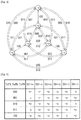
- FIG. 4 illustrates a relationship between the transition signals TxF, TxR, and TxP and symbol transition. Numerical values of three digits given to each transition indicate values of the transition signals TxF, TxR, and TxP in this order.
- the transition signal TxF may cause symbol transition between “+x” and “ ⁇ x”, between “+y” and “ ⁇ y”, and between “+z” and “ ⁇ z”. Specifically, when the transition signal TxF is “1”, the transition may take place to change polarity of the symbol (for example, from “+x” to “ ⁇ x”). When the transition signal TxF is “0”, such transition may not take place.
- the transition signals TxR (Rotation) and TxP (Polarity) may cause symbol transition between “+x” and a symbol other than “ ⁇ x”, between “+y” and a symbol other than “ ⁇ y”, and between “+z” and a symbol other than “ ⁇ z” when the signal TxF is “0”.
- the transition signals TxR and TxP are “1” and “0”, respectively, the transition may take place in a clockwise direction in FIG. 4 while keeping the polarity of the symbol (for example, transition from “+x” to “+y”).
- the transition signals TxR and TxP are “1” and “1”, respectively, the transition may take place in a clockwise direction in FIG.
- transition signals TxR and TxP are “0” and “0”, respectively, the transition may take place in a counterclockwise direction in FIG. 4 while keeping the polarity of the symbol (for example, transition from “+x” to “+z”).
- the transition signals TxR and TxP are “0” and “1”, respectively, the transition may take place in a counterclockwise direction in FIG. 4 while changing the polarity of the symbol (for example, transition from “+x” to “ ⁇ z”).
- the mapper 21 may generate seven sets of these transition signals TxF, TxR, and TxP. From among these seven sets of the transition signals TxF, TxR, and TxP (transition signals TxF 0 to TxF 6 , TxR 0 to TxR 6 , and TxP 0 to TxP 6 ), the mapper 21 may provide the transition signals TxF 0 to TxF 6 to the serializer 22 F; may provide the transition signals TxR 0 to TxR 6 to the serializer 22 R; and may provide the transition signals TxP 0 to TxP 6 to the serializer 22 P.
- the serializer 22 F may generate a transition signal TxF 9 by serializing the transition signals TxF 0 to TxF 6 in this order on the basis of the transition signals TxF 0 to TxF 6 and the clock signal TxCK.
- the serializer 22 R may generate a transition signal TxR 9 by serializing the transition signals TxR 0 to TxR 6 in this order on the basis of the transition signals TxR 0 to TxR 6 and the clock signal TxCK.
- the serializer 22 P may generate a transition signal TxP 9 by serializing the transition signals TxP 0 to TxP 6 in this order on the basis of the transition signals TxP 0 to TxP 6 and the clock signal TxCK.
- the transmission symbol generator 23 may generate symbol signals Tx 1 , Tx 2 , and Tx 3 on the basis of the transition signals TxF 9 , TxR 9 , and TxP 9 and the clock signal TxCK, and may output the symbol signals Tx 1 , Tx 2 , and Tx 3 as a transmission signal S 131 .
- the transmission symbol generator 23 may have a signal generator 24 and a flip-flop (F/F) 25 .
- the signal generator 24 may generate the symbol signals Tx 1 , Tx 2 , and Tx 3 on the basis of the transition signals TxF 9 , TxR 9 , and TxP 9 , and symbol signals D 1 , D 2 , and D 3 .
- the signal generator 24 may determine a symbol NS after transition as illustrated in FIG. 4 on the basis of a symbol (a symbol DS before transition) that the symbol signals D 1 , D 2 , and D 3 indicate, and the transition signals TxF 9 , TxR 9 , and TxP 9 to output the determined symbol DS as the symbol signals Tx 1 , Tx 2 , and Tx 3 .
- the flip-flop 25 may sample the symbol signals Tx 1 , Tx 2 , and Tx 3 on the basis of the clock signal TxCK to output sampling results as the symbol signals D 1 , D 2 , and D 3 , respectively.
- FIG. 5 illustrates an operation example of the transmission symbol generator 23 .
- FIG. 5 represents the symbols NS that are generated on the basis of the symbols DS indicated by the symbol signals D 1 , D 2 , and D 3 , and the transition signals TxF 9 , TxR 9 , and TxP 9 .
- the description is provided by citing an example where the symbol DS is “+x”.
- the symbol NS may be “+z”
- the transition signals TxF 9 , TxR 9 , and TxP 9 are “001”, respectively, the symbol NS may be “ ⁇ z”.
- the symbol NS When the transition signals TxF 9 , TxR 9 , and TxP 9 are “010”, respectively, the symbol NS may be “+y”, and when the transition signals TxF 9 , TxR 9 , and TxP 9 are “011”, respectively, the symbol NS may be “ ⁇ y”. When the transition signals TxF 9 , TxR 9 , and TxP 9 are “1xx”, respectively, the symbol NS may be “ ⁇ x”.
- “X” denotes that either “1” or “0” may be acceptable.
- the operation may be similar also in a case where the symbol DS is “ ⁇ x”, “+y”, “ ⁇ y”, “+z” or “ ⁇ z”.
- the transmission symbol generator 23 may generate the symbol signals Tx 1 , Tx 2 , and Tx 3 to output the resultant symbol signals Tx 1 , Tx 2 , and Tx 3 as the transmission signal S 131 . Thereafter, the transmission symbol generator 23 may provide the transmission signal S 131 to the driver controller 141 .
- the driver controller 141 may generate a signal S 141 on the basis of the transmission signal S 131 and the clock signal TxCK.
- the driver controller 142 may generate a signal S 142 on the basis of the transmission signal S 132 and the clock signal TxCK.
- the driver controller 143 may generate a signal S 143 on the basis of the transmission signal S 133 and the clock signal TxCK.
- Each of the signals S 141 , S 142 , and S 143 may have nine signals UPA, MDA, DNA, UPB, MDB, DNB, UPC, MDC, and DNC.
- the driver 151 may generate signals SIG 1 A, SIG 1 B, and SIG 1 C on the basis of the signal S 141 .
- the driver 152 may generate signals SIG 2 A, SIG 2 B, and SIG 2 C on the basis of the signal S 142 .
- the driver 153 may generate signals SIG 3 A, SIG 3 B, and SIG 3 C on the basis of the signal S 143 .
- FIG. 6 illustrates a configuration example of the driver 151 .
- the drivers 152 and 153 may each have a configuration similar to that of the driver 151 .
- the driver 151 may have drivers 151 A, 151 B, and 151 C.
- the driver 151 A may generate the signal SIG 1 A on the basis of the signals UPA, MDA, and DNA that are included in the signal S 141 .
- the driver 151 B may generate the signal SIG 1 B on the basis of the signals UPB, MDB, and DNB.
- the driver 151 C may generate the signal SIG 1 C on the basis of the signals UPC, MDC, and DNC.
- the driver 151 A may include an M-number of circuits VA (circuits UA 1 to UAM), an M-number of circuits UB (circuits UB 1 to UBM), an M-number of circuits DA (circuits DA 1 to DAM), an M-number of circuits DB (circuits DB 1 to DBM), and a transistor 95 .
- Each of the circuits UA 1 to UAM and UB 1 to UBM may have a transistor 91 and a resistor 92 .
- the transistor 91 may be an N-channel MOS (Metal-Oxide Semiconductor) FET (Field-Effect Transistor).
- the signal UPA may be supplied to a gate of the transistor 91 ; a voltage V 1 may be supplied to a drain thereof; and a source thereof may be coupled to a first end of the resistor 92 .
- the first end of the resistor 92 may be coupled to the source of the transistor 91 , and a second end thereof may be coupled to the output terminal Tout 1 A.
- a sum of an on-resistance of the transistor 91 and a resistance of the resistor 92 may be about “50 ⁇ 2M” ⁇ in this example.
- Each of the circuits DA 1 to DAM and DB 1 to DBM may have a resistor 93 and a transistor 94 .
- the transistor 94 may be an N-channel MOS FET.
- a first end of the resistor 93 may be coupled to the output terminal Tout 1 A, and a second end thereof may be coupled to a drain of the transistor 94 .
- the signal DNA may be supplied to a gate of the transistor 94 ; a drain thereof may be coupled to the second end of the resistor 93 ; and a source thereof may be grounded.
- a sum of a resistance of the resistor 93 and an on-resistance of the transistor 94 may be about “50 ⁇ 2M” ⁇ in this example.
- the transistor 95 may be an N-channel MOS FET in this example.
- the signal MDA may be supplied to a gate of the transistor 95 ; a drain thereof may be coupled to the output terminal Tout 1 A; and a signal Vdc having a voltage corresponding to the medium-level voltage VM may be supplied to a source thereof.
- FIG. 7 illustrates an operation example of the driver controller 141 and the driver 151 ,
- the operation may be similar also in the driver controller 142 and the driver 152 , as well as in the driver controller 143 and the driver 153 .
- the driver controller 141 may determine that the symbol to be outputted is “+x”, and may set the signals UPA, MDA, and DNA to “100” respectively, the signals UPB, MDB, and DNB to “001” respectively, and the signals UPC, MDC, and DNC to “010” respectively.
- the driver 151 A of the driver 151 this may turn on the transistor 91 in each of the circuits UA 1 to UAM and UB 1 to UBM. As a result, a voltage of the signal SIG 1 A may become the high-level voltage VH, and an output termination resistance (output impedance) of the driver 151 A may become about 50 ⁇ . Further, in the driver 151 B of the driver 151 , the transistor 94 in each of the circuits DA 1 to DAM and DB 1 to DBM may be turned on. As a result, a voltage of the signal SIG 1 B may become the low-level voltage VL, and an output termination resistance (output impedance) of the driver 151 B may become about 50 ⁇ .
- the transistor 95 may be turned on, and a voltage of the signal SIG 1 C may become the medium-level voltage VM. In such a manner, the driver 151 may generate the symbol “+x”. This may apply to other symbols as well.
- the voltage generator 16 may generate the signal Vdc having a voltage corresponding to the medium-level voltage VM.
- FIG. 8 illustrates a configuration example of the voltage generator 16 .
- the voltage generator 16 may have an M-number of circuits UC (circuits UC 1 to UCM) and an M-number of circuits DC (circuits DC 1 to DCM).
- the circuit UC may have a configuration similar to a configuration of each of the circuits UA and UB ( FIG. 6 ) in the driver 151
- the circuit DC may have a configuration similar to a configuration of each of the circuits DA and DB ( FIG. 6 ) in the driver 151 .
- the voltage V 1 may be supplied to a gate of a transistor 91 in each of the circuits UC 1 to UCM and a gate of a transistor 94 in each of the circuits DC 1 to DCM.
- a DC current IM may flow from a power source (voltage V 1 ) toward a ground through the circuits UC 1 to UCM and the circuits DC 1 to DCM.
- the voltage generator 16 may generate the signal Vdc having a voltage corresponding to the medium-level voltage VM, and an output impedance of the voltage generator 16 may become about 50 ⁇ .
- the reception device 30 may include receivers 31 , 32 , and 33 , and a processor 34 , as illustrated in FIG. 1 .
- the receiver 31 may receive the signals SIG 1 A, SIG 1 B, and SIG 1 C, and may generate a reception signal S 31 on the basis of these signals SIG 1 A, SIG 1 B, and SIG 1 C.
- the receiver 32 may receive the signals SIG 2 A, SIG 2 B, and SIG 2 C, and may generate a reception signal S 32 on the basis of these signals SIG 2 A, SIG 2 B, and SIG 2 C.
- the receiver 33 may receive the signals SIG 3 A, SIG 3 B, and SIG 3 C, and may generate a reception signal S 33 on the basis of these signals SIG 3 A, SIG 3 B, and SIG 3 C.
- FIG. 9 illustrates a configuration example of the receiver 31 .
- the receivers 32 and 33 may each have a configuration similar to that of the receiver 31 .
- the receiver 31 may include resistors 41 A, 41 B, and 41 C, switches 42 A, 42 B, and 42 C, amplifiers 43 A, 43 B, and 43 C, a clock generator 44 , flip-flops (F/Fs) 45 and 46 , and a signal generator 47 .
- the resistors 41 A, 41 B, and 41 C may function as termination resistors in the lane LN 1 , and may each have a resistance of about 50 ⁇ in this example.
- a first end of the resistor 41 A may be coupled to the input terminal Tin 1 A, and be supplied with the signal SIG 1 A, while a second end thereof may be coupled to a first end of the switch 42 A.
- a first end of the resistor 41 B may be coupled to the input terminal Tin 1 B, and be supplied with the signal SIG 1 B, while a second end thereof may be coupled to a first end of the switch 42 B.
- a first end of the resistor 41 C may be coupled to the input terminal Tin 1 C, and be supplied with the signal SIG 1 C, while a second end thereof may be coupled to a first end of the switch 42 C.
- the first end of the switch 42 A may be coupled to the second end of the resistor 41 A, and a second end thereof may be coupled to second ends of the switches 42 B and 42 C.
- the first end of the switch 42 B may be coupled to the second end of the resistor 41 B, and the second end thereof may be coupled to the second ends of the switches 42 A and 42 C.
- the first end of the switch 42 C may be coupled to the second end of the resistor 41 C, and the second end thereof may be coupled to the second ends of the switches 42 A and 42 B.
- the switches 42 A, 42 B, and 42 C may be set to an ON state, and the resistors 41 A to 41 C may function as termination resistors.
- a positive input terminal of the amplifier 43 A may be coupled to a negative input terminal of the amplifier 43 C and the first end of the resistor 41 A, and may be supplied with the signal SIG 1 A, while a negative input terminal thereof may be coupled to a positive input terminal of the amplifier 43 B and the first end of the resistor 41 B, and may be supplied with the signal SIG 1 B.
- the positive input terminal of the amplifier 43 B may be coupled to the negative input terminal of the amplifier 43 A and the first end of the resistor 41 B, and may be supplied with the signal SIG 1 B, while a negative input terminal thereof may be coupled to a positive input terminal of the amplifier 43 C and the first end of the resistor 41 C, and may be supplied with the signal SIG 1 C.
- the positive input terminal of the amplifier 43 C may be coupled to the negative input terminal of the amplifier 43 B and the first end of the resistor 41 C, and may be supplied with the signal SIG 1 C, and the negative input terminal thereof may be coupled to the positive input terminal of the amplifier 43 A and the first end of the resistor 41 A, and may be supplied with the signal SIG 1 A.
- the amplifier 43 A may output a signal corresponding to a difference AB (SIG 1 A ⁇ SIG 1 B) between the signal SIG 1 A and the signal SIG 1 B; the amplifier 43 B may output a signal corresponding to a difference BC (SIG 1 B ⁇ SIG 1 C) between the signal SIG 1 B and the signal SIG 1 C; and the amplifier 43 C may output a signal corresponding to a difference CA (SIG 1 C ⁇ SIG 1 A) between the signal SIG 1 C and the signal SIG 1 A.
- a difference AB SIG 1 A ⁇ SIG 1 B
- BC SIG 1 B ⁇ SIG 1 C
- CA SIG 1 C ⁇ SIG 1 A
- FIG. 10 illustrates an operation example of the amplifiers 43 A, 43 B, and 43 C in a case where the receiver 31 receives the symbol “+x”.
- the switches 42 A, 42 B, and 42 C remain in the ON state, and thus they are omitted in the illustration.
- a voltage of the signal SIG 1 A may be the high-level voltage VH
- a voltage of the signal SIG 1 B may be the low-level voltage VL
- a voltage of the signal SIG 1 C may be the medium-level voltage VM.
- a current Iin may flow through the input terminal Tin 1 A, the resistor 41 A, the resistor 41 B, and the input terminal Tin 1 B in this order.
- the amplifier 43 A may output “1”.
- the low-level voltage VL and the medium-level voltage VM are respectively provided to the positive input terminal and the negative input terminal of the amplifier 43 B to cause the difference BC to be negative (BC ⁇ 0)
- the amplifier 43 B may output “0”.
- the medium-level voltage VM and the high-level voltage VH are respectively provided to the positive input terminal and the negative input terminal of the amplifier 43 C to cause the difference CA to be negative (CA ⁇ 0)
- the amplifier 43 C may output “0”.
- the clock generator 44 may generate a clock signal RxCK on the basis of output signals of the amplifiers 43 A, 43 B, and 43 C.
- the flip-flop 45 may delay the output signals of the amplifiers 43 A, 43 B, and 43 C by one clock cycle of the clock signal RxCK to output each of such delayed output signals.
- the flip-flop 46 may delay three output signals of the flip-flop 45 by one clock cycle of the clock signal RxCK to output each of such delayed output signals.
- the signal generator 47 may generate transition signals RxF, RxR, and RxP on the basis of the output signals of the flip-flops 45 and 46 , and the clock signal RxCK.
- the transition signals RxF, RxR, and RxP may correspond to the transition signals TxF 9 , TxR 9 , and TxP 9 in the transmission device 10 , respectively ( FIG. 3 ), and may indicate symbol transition.
- the signal generator 47 may identify the symbol transition ( FIG. 4 ) on the basis of a symbol indicated by the output signals of the flip-flop 45 and a symbol indicated by the output signals of the flip-flop 46 to generate the transition signals RxF, RxR, and RxP.
- the receiver 31 may generate the transition signals RxF, RxR, and RxP, and the clock signal RxCK on the basis of the signals SIG 1 A, SIG 1 B, and SIG 1 C. Thereafter, the receiver 31 may output the transition signals RxF, RxR, and RxP, and the clock signal RxCK as the reception signal S 31 .
- the processor 34 may perform predetermined processing operation on the basis of the reception signals S 31 , S 32 , and S 33 .
- the driver 151 corresponds to a specific but not limitative example of a “first transmitter” in one embodiment of the present disclosure.
- the driver 152 corresponds to a specific but not limitative example of a “second transmitter” in one embodiment of the present disclosure.
- the transistor 95 corresponds to a specific but not limitative example of a “switch” in one embodiment of the present disclosure.
- the voltage generator 16 corresponds to a specific but not limitative example of a “voltage generator” in one embodiment of the present disclosure.
- the clock generator 11 of the transmission device 10 may generate the clock signal TxCK.
- the processor 12 may generate respective data to be transmitted using the lanes LN 1 , LN 2 , and LN 3 by performing pre-determined processing operation. Thereafter, the processor 12 may provide the data to be transmitted using the lane LN 1 to the transmission signal generator 131 ; may provide the data to be transmitted using the lane LN 2 to the transmission signal generator 132 ; and may provide the data to be transmitted using the lane LN 3 to the transmission signal generator 133 .
- the transmission signal generator 131 may generate the transmission signal S 131 on the basis of the data provided from the processor 12 .
- the transmission signal generator 132 may generate the transmission signal S 132 on the basis of the data provided from the processor 12 .
- the transmission signal generator 133 may generate the transmission signal S 133 on the basis of the data provided from the processor 12 .
- the mapper 21 may generate the transition signals TxF 0 to TxF 6 , TxR 0 to TxR 6 , and TxP 0 to TxP 6 by performing predetermined mapping processing operation on the basis of the data provided from the processor 12 , and the clock signal TxCK.
- the serializer 22 F may generate the transition signal TxF 9 on the basis of the transition signals TxF 0 to TxF 6 and the clock signal TxCK.
- the serializer 22 R may generate the transition signal TxR 9 on the basis of the transition signals TxR 0 to TxR 6 and the clock signal TxCK.
- the serializer 22 P may generate the transition signal TxP 9 on the basis of the transition signals TxP 0 to TxP 6 and the clock signal TxCK.
- the transmission symbol generator 23 may generate the symbol signals Tx 1 , Tx 2 , and Tx 3 on the basis of the transition signals TxF 9 , TxR 9 , and TxP 9 , and the clock signal TxCK to output the resultant symbol signals Tx 1 , Tx 2 , and Tx 3 as the transmission signals S 131 .
- the driver controller 141 may generate the signal S 141 on the basis of the transmission signal S 131 and the clock signal TxCK.
- the driver controller 142 may generate the signal S 142 on the basis of the transmission signal S 132 and the clock signal TxCK.
- the driver controller 143 may generate the signal S 143 on the basis of the transmission signal S 133 and the clock signal TxCK.
- the voltage generator 16 may generate the signal Vdc having a voltage corresponding to the medium-level voltage VM.
- the driver 151 may generate the signals SIG 1 A, SIG 1 B, and SIG 1 C on the basis of the signal S 141 and the signal Vdc.
- the driver 152 may generate the signals SIG 2 A, SIG 2 B, and SIG 2 C on the basis of the signal S 142 and the signal Vdc.
- the driver 153 may generate the signals SIG 3 A, SIG 3 B, and SIG 3 C on the basis of the signal S 143 and the signal Vdc.
- the receiver 31 may generate the reception signal S 31 on the basis of the signals SIG 1 A, SIG 1 B, and SIG 1 C; the receiver 32 may generate the reception signal S 32 on the basis of the signals SIG 2 A, SIG 2 B, and SIG 2 C; and the receiver 33 may generate the reception signal S 33 on the basis of the signals SIG 3 A, SIG 3 B, and SIG 3 C.
- the processor 34 may perform predetermined processing operation on the basis of the reception signals S 31 to S 33 .
- the voltage generator 16 may generate the signal Vdc having a voltage corresponding to the medium-level voltage VM. Thereafter, the driver 151 may generate the signals SIG 1 A, SIG 1 B, and SIG 1 C on the basis of the signal S 141 and the signal Vdc; the driver 152 may generate the signals SIG 2 A, SIG 2 B, and SIG 2 C on the basis of the signal S 142 and the signal Vdc; and the driver 153 may generate the signals SIG 3 A, SIG 3 B, and SIG 3 C on the basis of the signal S 143 and the signal Vdc.
- this operation is described in detail.
- FIG. 11 illustrates an operation example of the driver 151 in outputting the symbol “+x”.
- each of circuits indicated with solid lines among the circuits UA 1 to UAM and UB 1 to UBM represents a circuit in which the transistor 91 is in an ON state
- each of circuits indicated with dashed lines represents a circuit in which the transistor 91 is in an OFF state.
- each of circuits indicated with solid lines among the circuits DA 1 to DAM and DB 1 to DBM represents a circuit in which the transistor 94 is in the ON state
- each of circuits indicated with dashed lines represents a circuit in which the transistor 94 is in the OFF state.
- each of the circuits UC is indicated with a solid line because the transistor 91 is in the ON state
- each of the circuits DC is indicated with a solid line because the transistor 94 is in the ON state.
- each of the transistors 95 is illustrated with a switch indicating an operating state thereof.
- the driver controller 141 may set the signals UPA, MDA, and DNA to “100” respectively, the signals UPB, MDB, and DNB to “001” respectively, and the signals UPC, MDC, and DNC to “010” respectively, as illustrated in FIG. 7 .
- the transistor 91 in each of the circuits UA 1 to UAM and UB 1 to UBM may turn on, while the transistor 94 in each of the circuits DA 1 to DAM and DB 1 to DBM may turn off, and the transistor 95 may turn off. Consequently, a voltage of the signal SIG 1 A may become the high-level voltage VH, and an output termination resistance (output impedance) of the driver 151 A may become about 50 ⁇ .
- the transistor 91 in each of the circuits UA 1 to UAM and UB 1 to UBM may be turned off, while the transistor 94 in each of the circuits DA 1 to DAM and DB 1 to DBM may be turned on, and the transistor 95 may be turned off. Consequently, a voltage of the signal SIG 1 B may become the low-level voltage VL, and an output termination resistance (output impedance) of the driver 151 B may become about 50 ⁇ .
- the transistor 91 in each of the circuits UA 1 to UAM and UB 1 to UBM may be turned off, while the transistor 94 in each of the circuits DA 1 to DAM and DB 1 to DBM may be turned off, and the transistor 95 may be turned on. Consequently, in the driver 151 C, the signal Vdc that is generated by the voltage generator 16 may be provided to the output terminal Tout 1 C, and a voltage of the output terminal Tout 1 C may be set to the medium-level voltage VM. Meanwhile, in the receiver 31 of the reception device 30 , the high-level voltage VH may be applied to the first end of the resistor 41 A, and the low-level voltage VH may be applied to the first end of the resistor 41 B.
- a voltage (the medium-level voltage VM) that is divided by these resistors 41 A and 41 B may be provided to the input terminal Tin 1 C through the resistor 41 C.
- a voltage of the output terminal Tout 1 C and a voltage of the input terminal Tin 1 C are almost equal to each other, and therefore a current may hardly flow through the line path 101 C.
- a voltage of the signal SIG 1 C may become the medium-level voltage VM.
- the voltage generator 16 may provide the signal Vdc to not only the driver 151 but also the drivers 152 and 153 , as illustrated in FIG. 1 .
- the single voltage generator 16 may be provided for the three drivers 151 , 152 , and 153 . Therefore, when communication is performed in the communication system 1 using the three lanes LN 1 , LN 2 , and LN 3 , these three lanes LN 1 , LN 2 , and LN 3 are likely to have an influence on one another.
- FIG. 12 illustrates an example of an eye diagram in the lane LN 1 in a case where the communication is performed using the three lanes LN 1 , LN 2 , and LN 3 .
- FIG. 12 illustrates eye diagrams of the difference AB between the signal SIG 1 A and the signal SIG 1 B, the difference BC between the signal SIG 1 B and the signal SIG 1 C, and the difference CA between the signal SIG 1 C and the signal SIG 1 A.
- the communication is performed using the three lanes LN 1 , LN 2 , and LN 3 , it is possible to assure sufficient eye apertures in the communication system 1 , which makes it possible to suppress deterioration in waveform quality.
- the single voltage generator 16 is provided for the three drivers 151 , 152 , and 153 , which makes it possible to reduce power consumption while suppressing deterioration in the communication performance, as compared with a comparative example to be described below.
- a method of generating the medium-level voltage VM may be different from the method in the communication system 1 .
- the communication system 1 R includes a transmission device 10 R and a reception device 30 .
- the transmission device 10 R is configured in such a manner that the voltage generator 16 is eliminated; the driver controllers 141 , 142 , and 143 are replaced with driver controllers 141 R, 142 R, and 143 R, respectively; and the drivers 151 , 152 , and 153 are replaced with drivers 151 R, 152 R, and 153 R, respectively in the transmission device 10 according to the present embodiment ( FIG. 1 ).
- the driver controller 141 R generates a signal S 141 R on the basis of the transmission signal S 131 and the clock signal TxCK.
- the driver controller 142 R generates a signal S 142 R on the basis of the transmission signal S 132 and the clock signal TxCK.
- the driver controller 143 R generates a signal S 143 R on the basis of the transmission signal S 133 and the clock signal TxCK.
- Each of the signals S 141 R, S 142 R, and S 143 R has twelve signals UPAA, UPAB, DNAA, DNAB, UPBA, UPBB, DNBA, DNBB, UPCA, UPCB, DNCA, and DNCB.
- the driver 151 R generates signals SIG 1 A, SIG 1 B, and SIG 1 C on the basis of the signal S 141 R.
- the driver 152 R generates signals SIG 2 A, SIG 2 B, and SIG 2 C on the basis of the signal S 142 R.
- the driver 153 B generates signals SIG 3 A, SIG 3 B, and SIG 3 C on the basis of the signal S 143 R.
- FIG. 13 illustrates a configuration example of the driver 151 R.
- the configuration is similar also in the drivers 152 R and 153 R.
- the driver 151 R has drivers 151 RA, 151 RB, and 151 RC.
- the driver 151 RA generates the SIG 1 A on the basis of the signals UPAA, UPAB, DNAA, and DNAB that are included in the signal S 141 R.
- the driver 151 RB generates the SIG 1 B on the basis of the signals UPBA, UPBB, DNBA, and DNBB.
- the driver 151 RC generates the SIG 1 C on the basis of the signals UPCA, UPCB, DNCA, and DNCB.
- the driver 151 RA includes an M-number of circuits VA (circuits UA 1 to UAM), an M-number of circuits UB (circuits UB 1 to UBM), an M-number of circuits DA (circuits DA 1 to DAM), and an M-number of circuits DB (circuits DB 1 to DBM).
- the signal UPAA is supplied to a gate of a transistor 91 in each of the circuits UA 1 to UAM
- the signal UPAB is supplied to a gate of a transistor 91 in each of the circuits UB 1 to UBM.
- the signal DNAA is supplied to a gate of a transistor 94 in each of the circuits DA 1 to DAM, and the signal DNAB is supplied to a gate of a transistor 94 in each of the circuits DB 1 to DBM. This applies to the driver 151 RB and the driver 151 RC as well.
- FIG. 14 illustrates an operation example of the driver 151 R in outputting the symbol “+x”.
- the driver controller 141 R may set the signals UPAA, UPAB, DNAA, and DNAB to “1100” respectively, the signals UPBA, UPBB, DNBA, and DNBB to “0011” respectively, and the signals UPCA, UPCB, DNCA, and DNCB to “1010” respectively, for example.
- the transistor 91 in each of the circuits UA 1 to LAM and UB 1 to UBM may be turned on, and the transistor 94 in each of the circuits DA 1 to DAM and DB 1 to DBM may be turned off. Consequently, a voltage of the signal SIG 1 A may become the high-level voltage VH, and an output termination resistance (output impedance) of the driver 151 RA may become about 50 ⁇ . Further, in the driver 151 RB, the transistor 91 in each of the circuits UA 1 to UAM and UB 1 to UBM may be turned off, and the transistor 94 in each of the circuits DA 1 to DAM and DB 1 to DBM may be turned on.
- a voltage of the signal SIG 1 B may become the low-level voltage VL, and an output termination resistance (output impedance) of the driver 151 RB may become about 50 ⁇ .
- the transistor 91 in each of the circuits UA 1 to UAM and the transistor 94 in each of the circuits DA 1 to DAM may be turned on, and the transistor 91 in each of the circuits UB 1 to UBM and the transistor 94 in each of the circuits DB 1 to DBM may be turned off. Consequently, a voltage of the signal SIG 1 C may become the medium-level voltage VM, and an output termination resistance (output impedance) of the driver 151 RC may become about 50 ⁇ .
- the transistor 91 in each of the circuits UA 1 to UAM and the transistor 94 in each of the circuits DA 1 to DAM may be turned on.
- an output terminal Tout 1 C of the driver 151 RC may be pulled up by a resistor of about 100 ⁇ , and be pulled down by a resistor of about 100 ⁇ . Consequently, a DC current IM may flow through the driver 151 RC via these two resistors.
- the DC current IM may flow through a single driver in the driver 151 R; the DC current IM may flow through a single driver in the driver 152 R; and the DC current IM may flow through a single driver in the driver 153 R. This may result in an increase in power consumption.
- the single voltage generator 16 is provided for the three drivers 151 , 152 , and 153 . This makes it possible to reduce power consumed by the DC current IM, and to reduce power consumption in the transmission device 10 .
- the single voltage generator is provided for a plurality of drivers, which makes it possible to reduce power consumption.
- the signal Vdc is generated by resistance voltage division; however, a method is not limited thereto.
- the signal Vdc may be generated with use of a regulator.
- the voltage generator 16 A may include a reference voltage generator 51 , an operational amplifier 52 , a capacitor 53 , and a resistor 54 .
- the reference voltage generator 51 may be configured to include, for example, a bandgap reference circuit, and may generate a reference voltage Vref corresponding to the medium-level voltage VM.
- the reference voltage Vref may be provided to a positive input terminal of the operational amplifier 52 , and a negative input terminal thereof may be coupled to an output terminal thereof.
- the operational amplifier 52 may operate as a voltage-follower to output the signal Vdc having a voltage corresponding to the medium-level voltage VM. Even when such a voltage generator 16 A is used, it is similarly possible to assure sufficient eye apertures as illustrated in FIG. 16 , which makes it possible to suppress deterioration in waveform quality.
- the output impedance of the voltage generator 16 is set to about 50 ⁇ ; however, the present embodiment is not limited thereto. Alternatively, for example, the output impedance of the voltage generator may be sufficiently reduced, and a termination resistor of about 50 ⁇ may be provided in each driver.
- a communication system 1 B according to the present modification example is described in detail.
- the communication system 1 B may include a transmission device 10 B and the reception device 30 .
- the transmission device 10 B may have drivers 251 , 252 , and 253 , and a voltage generator 16 B.
- FIG. 17 illustrates a configuration example of the driver 251 .
- the drivers 252 and 253 may each have a configuration similar to that of the driver 251 .
- the driver 251 may have drivers 251 A, 251 B, and 251 C.
- the driver 251 A may have a resistor 96 .
- a first end of the resistor 96 may be coupled to the drain of the transistor 95 , and a second end thereof may be coupled to the output terminal Tout 1 A.
- a resistance of the resistor 96 may be about 50 ⁇ . This may apply to the drivers 251 B and 251 C as well.
- FIG. 18 illustrates a configuration example of the voltage generator 16 B.
- the voltage generator 16 B may have resistors 55 and 56 , and a capacitor 57 .
- the voltage VI may be supplied to a first end of the resistor 55 , and a second end thereof may be coupled to a first end of the resistor 56 and a first end of the capacitor 57 .
- the first end of the resistor 56 may be coupled to the second end of the resistor 55 and the first end of the capacitor 57 , and a second end thereof may be grounded.
- a resistance of each of the resistors 55 and 56 may be set to an equal value. Specifically, it may be possible to set the resistance of each of the resistors 55 and 56 to several k ⁇ , for example.
- the first end of the capacitor 57 may be coupled to the second end of the resistor 55 and the first end of the resistor 56 , and the second end thereof may be grounded.
- the voltage generator 16 B makes it possible to generate the signal Vdc having a voltage corresponding to the medium-level voltage VM, as well as to reduce an output impedance of the voltage generator 16 B in a frequency range of signals to be transmitted by the communication system 1 B.
- the communication system 1 B makes it possible to reduce the amount of the DC current IM in the voltage generator 16 B, which allows for reduction in power consumption. Further, each of the drivers 251 A, 251 B, and 251 C has the resistor 96 , and therefore even if the communication is performed using, for example, the three lanes LN 1 , LN 2 , and LN 3 , it is possible to enhance the isolation of the lanes from one. another, which allows for improvement in waveform quality.
- the voltage generator 16 B ( FIG. 18 ) is used in this example; however, a configuration is not limited thereto.
- a voltage generator 16 C illustrated in FIG. 19 may be used.
- the voltage generator 16 C may include the reference voltage generator 51 , the operational amplifier 52 , and a capacitor 53 .
- the voltage generator 16 C may be equivalent to the voltage generator 16 A ( FIG. 15 ) from which the resistor 54 is omitted.
- the present embodiment may use a transmission device having an operation mode of performing communication with use of a signal having three voltage levels and an operation mode of performing communication with use of a differential signal. It is to be noted that any component parts essentially same as those in the communication system 1 according to the above-described first embodiment are denoted with the same reference numerals, and the related descriptions are omitted as appropriate.
- FIG. 20A illustrates a configuration example of the communication system 2 A according to the present embodiment.
- FIG. 20B illustrates a configuration example of the communication system 2 B according to the present embodiment.
- the communication system 2 A may include a transmission device 60 , a transmission line 100 , and a reception device 30 .
- the communication system 2 A may perform communication with use of a signal having three voltage levels.
- the communication system 2 B may include the transmission device 60 , the transmission line 110 , and the reception device 70 .
- the communication system 2 B may perform communication with use of a differential signal.
- the transmission device 60 may have two operation modes MA and MB.
- the transmission device 60 may operate in the operation mode MA when the transmission device 60 is applied to the communication system 2 A, and may operate in the operation mode MB when the transmission device 60 is applied to the communication system 2 B.
- the communication system 2 A may operate in a manner similar to the communication system 1 according to the above-described embodiment.
- the communication system 2 A may use the lane LN 1 to transmit the signal SIG 1 A through the line path 101 A; to transmit the signal SIG 1 B through the line path 101 B; and to transmit the signal SIG 1 C through the line path 101 C.
- the communication system 2 A may use the lane LN 2 to transmit the signal SIG 2 A through the line path 102 A; to transmit the signal SIG 2 B through the line path 102 B; and to transmit the signal SIG 2 C through the line path 102 C.
- the communication system 2 A may use the lane LN 3 to transmit the signal SIG 3 A through the line path 103 A; to transmit the signal SIG 3 B through the line path 103 B; and to transmit the signal SIG 3 C through the line path 103 C.
- the transmission line 110 may have line paths 111 P and 111 N, line paths 112 P and 112 N, line paths 113 P and 113 N, and line paths 114 P and 114 N.
- the reception device 70 may have input terminals Tin 1 P and Tin 1 N, input terminals Tin 2 P and Tin 2 N, input terminals Tin 3 P and Tin 3 N, and input terminals Tin 4 P and Tin 4 N.
- An output terminal Tout 1 A of the transmission device 60 and the input terminal Tin 1 P of the reception device 70 may be coupled to each other through the line path 111 P
- an output terminal Tout 1 B of the transmission device 60 and the input terminal Tin 1 N of the reception device 70 may be coupled to each other through the line path 111 N.
- an output terminal Tout 1 C of the transmission device 60 and the input terminal Tin 2 P of the reception device 70 may be coupled to each other through the line path 112 P, and an output terminal Tout 2 A of the transmission device 60 and the input terminal Tin 2 N of the reception device 70 may be coupled to each other through the line path 112 N.
- an output terminal Tout 2 B of the transmission device 60 and the input terminal Tin 3 P of the reception device 70 may be coupled to each other through the line path 113 P, and an output terminal Tout 2 C of the transmission device 60 and the input terminal Tin 3 N of the reception device 70 may be coupled to each other through the line path 113 N.
- an output terminal Tout 3 A of the transmission device 60 and the input terminal Tin 4 P of the reception device 70 may be coupled to each other through the line path 114 P
- an output terminal Tout 3 B of the transmission device 60 and the input terminal Tin 4 N of the reception device 70 may be coupled to each other through the line path 114 N.
- a characteristic impedance of each of the line paths 111 P, 111 N, 112 P, 112 N, 113 P, 113 N, 114 P, and 114 N may be about 50 ⁇ in this example.
- the line, paths 111 P and 111 N may configure a lane LN 11 ; the line paths 112 P and 112 N may configure a lane LN 12 ; the line paths 113 P and 113 N may configure a lane LN 13 ; and the line paths 114 P and 114 N may configure a lane LN 14 .
- the communication system 2 B may use the lane LN 11 to transmit a signal SIG 1 P through the line path 111 P, and to transmit a signal SIG 1 N through the line path 111 N.
- the communication system 2 B may use the lane LN 12 to transmit a signal SIG 2 P through the line path 112 P, and to transmit a signal SIG 2 N through the line path 112 N.
- the communication system 2 B may use the lane LN 13 to transmit a signal SIG 3 P through the line path 113 P, and to transmit a signal SIG 3 N through the line path 113 N.
- the communication system 2 B may use the lane LN 14 to transmit a signal SIG 4 P through the line path 114 P, and to transmit a signal SIG 4 N through the line path 114 N.
- the signals SIG 1 P and SIG 1 N may configure a differential signal; the signals SIG 2 P and SIG 2 N may configure a differential signal; the signals SIG 3 P and SIG 3 N may configure a differential signal; and the signals SIG 4 P and SIG 4 N may configure a differential signal.
- FIG. 21 illustrates a configuration example of the transmission device 60 .
- the transmission device 60 may include a processor 62 , transmission signal generators 181 to 184 , and selectors 191 to 199 .
- the processor 62 may generate data to be transmitted by performing predetermined processing operation. Further, the processor 62 may select one of the two operation modes MA and MB, and may control the transmission device 60 to operate in the selected operation mode. Specifically, when the transmission device 60 is applied to the communication system 2 A ( FIG. 20A ), the processor 62 may select the operation mode MA to set a signal SET to “1”, and may generate respective data to be transmitted using the lanes LN 1 , LN 2 , and LN 3 .
- the processor 62 may provide data to be transmitted using the lane LN 1 to the transmission signal generator 131 ; may provide data to be transmitted using the lane LN 2 to the transmission signal generator 132 ; and may provide data to be transmitted using the lane LN 3 to the transmission signal generator 133 .
- the processor 62 may select the operation mode MB to set the signal SET to “0”, and may generate respective data to be transmitted using the lanes LN 11 , LN 12 , LN 13 , and LN 14 .
- the processor 62 may provide data to be transmitted using the lane LN 11 to the transmission signal generator 181 ; may provide data to be transmitted using the lane LN 12 to the transmission signal generator 182 ; may provide data to be transmitted using the lane LN 13 to the transmission signal generator 183 , and may provide data to be transmitted using the lane LN 14 to the transmission signal generator 184 .
- the transmission signal generator 181 may generate a transmission signal S 181 on the basis of the data provided from the processor 62 and the clock signal TxCK.
- the transmission signal generator 182 may generate a transmission signal S 182 on the basis of the data provided from the processor 62 and the clock signal TxCK.
- the transmission signal generator 183 may generate a transmission signal S 183 on the basis of the data provided from the processor 62 and the clock signal TxCK.
- the transmission signal generator 184 may generate a transmission signal S 184 on the basis of the data provided from the processor 62 and the clock signal TxCK.
- FIG. 22 illustrates a configuration example of the transmission signal generator 181 .
- the transmission signal generators 182 to 184 may each have a configuration similar to that of the transmission signal generator 181 .
- the transmission signal generator 181 may have a pattern generator 63 , a selector 64 , and a serializer 65 .
- the pattern generator 63 may generate a data pattern to be used in performing deskew of the lanes LN 11 to LN 14 in, for example, the communication system 2 B ( FIG. 20B ) on the basis of the clock signal TxCK.
- the selector 64 may select one of the data provided from the processor 62 and the data generated by the pattern generator 63 on the basis of, for example, a control signal (not illustrated) that is provided from the processor 62 to output the selected data as a signal S 64 .
- the serializer 65 may serialize data (a parallel signal) that is provided from the selector 64 on the basis of the clock signal TxCK, thereby generating a signal S 181 .
- the signal S 181 may include signals UP and DN that are inverted to each other.
- Each of selectors 191 to 199 may control operation of each of the drivers 151 to 153 on the basis of the signal SEL, and the signals S 141 to S 143 and S 181 to S 184 .
- FIG. 23 illustrates an operation example of each of the selectors 191 to 199 .
- the selector 191 may output the signal UPA included in the signal S 141 as a signal UP 1 ; may output the signal MDA as a signal MD 1 and may output the signal DNA as a signal DN 1 .
- the driver 151 A may generate the signal SIG 1 A on the basis of the signals UP 1 , MD 1 , and DN 1 . For example, when the signal MD 1 is “1”, the transistor 95 in the driver 151 A may turn on, thereby setting the voltage of signal SIG 1 A to the medium-level voltage VM, as with the above-described first embodiment.
- the selector 191 may output the signal UP included in the signal S 181 as the signal UP 1 ; may output the signal DN as the signal DN 1 ; and may set the signal MD 1 to “0” (low level).
- the driver 151 A may generate the signal SIG 1 P on the basis of the signals UP 1 , MD 1 , and DN 1 . As a result, in the operation mode MB, the transistor 95 in the driver 151 A may remain in the OFF state.
- the selector 192 may output a signal UPB included in the signal S 141 as a signal UP 2 ; may output a signal MDB as a signal MD 2 ; and may output the signal DNB as a signal DN 2 .
- the driver 151 E may generate the signal SIG 1 B on the basis of the signals UP 2 , MD 2 , and DN 2 .
- the selector 192 may output the signal DN included in the signal S 181 as the signal UP 2 ; may output the signal UP as the signal DN 2 ; and may set the signal MD 2 to “0” (low level).
- the driver 151 B may generate the signal SIG 1 N on the basis of the signals UP 2 , MD 2 , and DN 2 .
- the selector 193 may output the signal UPC included in the signal S 141 as a signal UP 3 ; may output the signal MDC as a signal MD 3 ; and may output the signal DNC as a signal DN 3 .
- the driver 151 C may generate the signal SIG 1 C on the basis of the signals UP 3 , MD 3 , and DN 3 .
- the selector 193 may output the signal UP included in the signal S 182 as the signal UP 3 ; may output the signal DN as the signal DN 3 ; and may set the signal MD 3 to “0” (low level).
- the driver 151 C may generate the signal SIG 2 P on the basis of the signals UP 3 , MD 3 , and DN 3 .
- the selector 194 may output a signal UPA included in the signal S 142 as a signal UP 4 ; may output a signal MDA as a signal MD 4 ; and may output the signal DNA as a signal DN 4 .
- a driver 152 A may generate the signal SIG 2 A on the basis of the signals UP 4 , MD 4 , and DN 4 .
- the selector 194 may output the signal DN included in the signal S 182 as the signal UP 4 ; may output the signal UP as the signal DN 4 ; and may set the signal MD 4 to “0” (low level).
- the driver 152 A may generate the signal SIG 2 N on the basis of the signals UP 4 , MD 4 , and DN 4 .
- the selector 195 may output the signal UPB included in the signal S 142 as a signal UP 5 ; may output a signal MDB as a signal MD 5 ; and may output the signal DNB as a signal DN 5 .
- a driver 152 B may generate the signal SIG 2 B on the basis of the signals UP 5 , MD 5 , and DN 5 .
- the selector 195 may output the signal UP included in the signal S 183 as the signal UP 5 ; may output the signal DN as the signal DN 5 ; and may set the signal MD 5 to “0” (low level).
- the driver 152 B may generate the signal SIG 3 P on the basis of the signals UP 5 , MD 5 , and DN 5 .
- the selector 196 may output the signal UPC included in the signal S 142 as a signal UP 6 ; may output the signal MDC as a signal MD 6 ; and may output the signal DNC as a signal DN 6 .
- a driver 152 C may generate the signal SIG 2 C on the basis of the signals UP 6 , MD 6 , and DN 6 .
- the selector 196 may output the signal DN included in the signal S 183 as the signal UP 6 ; may output the signal UP as the signal DN 6 ; and may set the signal MD 6 to “0” (low level).
- the driver 152 C may generate the signal SIG 3 N on the basis of the signals UP 6 , MD 6 , and DN 6 .
- the selector 197 may output the signal UPA included in the signal S 143 as a signal UP 7 ; may output the signal MDA as a signal MD 7 ; and may output the signal DNA as a signal DN 7 .
- a driver 153 A may generate the signal SIG 3 A on the basis of the signals UP 7 , MD 7 , and DN 7 .
- the selector 197 may output the signal UP included in the signal S 184 as the signal UP 7 ; may output the signal DN as the signal DN 7 ; and may set the signal MD 7 to “0” (low level).
- the driver 153 A may generate the signal SIG 4 P on the basis of the signals UP 7 , MD 7 , and DN 7 .
- the selector 198 may output the signal UPB included in the signal S 143 as a signal UP 8 ; may output the signal MDB as a signal MD 8 ; and may output the signal DNB as a signal DN 8 .
- a driver 153 B may generate the signal SIG 3 B on the basis of the signals UP 8 , MD 8 , and DN 8 .
- the selector 198 may output the signal DN included in the signal S 184 as the signal UP 8 ; may output the signal UP as the signal DN 8 ; and may set the signal MD 8 to “0” (low level).
- the driver 153 B may generate the signal SIG 4 N on the basis of the signals UP 8 , MD 8 , and DN 8 .
- the selector 199 may output the signal UPC included in the signal S 143 as a signal UP 9 ; may output the signal MDC as a signal MD 9 ; and may output the signal DNC as a signal DN 9 .
- a driver 153 C may generate the signal SIG 3 C on the basis of the signals UP 9 , MD 9 , and DN 9 .
- the selector 199 may set each of the signals UP 9 , MD 9 , and DN 9 to “0” (low level).
- the reception device 70 may include receivers 71 , 72 , 73 , and 74 , and a processor 75 .
- the receiver 71 may receive the signals SIG 1 P and SIG 1 N, and may generate a reception signal S 71 on the basis of these signals SIG 1 P and SIG 1 N.
- the receiver 72 may receive the signals SIG 2 P and SIG 2 N, and may generate a reception signal S 72 on the basis of these signals SIG 2 P and SIG 2 N.
- the receiver 73 may receive the signals SIG 3 P and SIG 3 N, and may generate a reception signal S 73 on the basis of these signals SIG 3 P and SIG 3 N.
- the receiver 74 may receive the signals SIG 4 P and SIG 4 N, and may generate a reception signal S 74 on the basis of these signals SIG 4 P and SIG 4 N.
- FIG. 24 illustrates a configuration example of the receiver 71 .
- the receivers 72 to 74 may each have a configuration similar to that of the receiver 71 .
- the receiver 71 may include a resistor 81 , an amplifier 82 , a clock generator 83 , and a flip-flop (F/F) 84 .
- the resistor 81 may function as a termination resistor in the lane LN 11 , and may have a resistance of about 100 ⁇ in this example.
- a first end of the resistor 81 may be coupled to the input terminal Tin 1 P, and be supplied with the signal SIG 1 P, while a second end thereof may be coupled to the input terminal Tin 1 N, and be supplied with the signal SIG 1 N.
- a positive input terminal of the amplifier 82 may be coupled to the first end of the resistor 81 , and be supplied with the signal SIG 1 P, while a negative input terminal thereof may be coupled to the second end of the resistor 81 , and be supplied with the signal SIG 1 N.
- the clock generator 83 may generate the clock signal RxCK on the basis of an output signal of the amplifier 82 .
- the flip-flop 84 may sample the output signal of the amplifier 82 at a transition timing of the clock signal RxCK to output a sampling result as a data signal RxD.
- the receiver 71 may generate the data signal RxD and the clock signal RxCK on the basis of the signals SIG 1 P and SIG 1 N. Thereafter, the receiver 71 may output the data signal RxD and the clock signal RxCK as the reception signal S 71 .
- the processor 75 may perform predetermined processing operation on the basis of the reception signals S 71 to S 74 .
- a plurality of operation modes (two operation modes M 1 and M 2 in this example) are provided, which makes it possible to achieve various interfaces.
- FIG. 25 illustrates an external appearance of a smartphone 300 (multifunctional mobile phone) to which the communication system according to any of the above-described embodiments and the modification examples thereof is applied.
- a smartphone 300 multifunctional mobile phone
- a variety of devices are built into this smartphone 300 , and the communication system according to any of the above-described embodiments and the modification examples thereof is applied to a communication system that exchanges data between these devices.
- FIG. 26 illustrates a configuration example of an application processor 310 used in the smartphone 300 .
- the application processor 310 has a CPU (Central Processing Unit) 311 , a memory controller 312 , a power source controller 313 , an external interface 314 , a GPU (Graphics Processing Unit) 315 , a media processing controller 316 , a display controller 317 , and an MIPI (Mobile Industry Processor Interface) interface 318 .
- the CPU 311 , the memory controller 312 , the power source controller 313 , the external interface 314 , the GPU 315 , the media processor 316 , and the display controller 317 are coupled to a system bus 319 to allow for data exchange therebetween via this system bus 319 .
- a system bus 319 to allow for data exchange therebetween via this system bus 319 .
- the CPU 311 may process various information to be handled in the smartphone 300 in accordance with a program.
- the memory controller 312 may control a memory 501 to be used when the CPU 311 performs information processing operation.
- the power source controller 313 may control a power source of the smartphone 300 .
- the external interface 314 is an interface for communication with external devices, and may be coupled to a wireless communication section 502 and an image sensor 410 in this example.
- the wireless communication section 502 may perform wireless communication with mobile phone base stations, and may include, for example, a baseband section and an RF (Radio Frequency) front-end section.
- the image sensor 410 may acquire an image, and may include, for example, a CMOS sensor.
- the GPU 315 may perform image processing operation.
- the media processor 316 processes information such as voice, characters, and graphics.
- the display controller 317 controls a display 504 via the MIDI interface 318 .
- the interface 318 transmits an image signal to the display 504 .
- an image signal for example, a YUV-format signal, a RGB-format signal, or any other format signal may be used.
- the MIPI interface 318 may operate on the basis of a reference clock to be provided from an oscillator circuit 330 including, for example, a crystal oscillator.
- the communication system according to any of the above-described embodiments and the modification examples thereof may be applied to a communication system between the MIPI interface 318 and the display 504 .
- FIG. 27 illustrates a configuration example of the image sensor 410 .
- the image sensor 410 has a sensor 411 , an ISP (Image Signal Processor) 412 , a JPEG (Joint Photographic Experts Group) encoder 413 , a CPU 414 , a RAM (Random Access Memory) 415 , a ROM (Read Only Memory) 416 , a power source controller 417 , an I 2 C (Inter-Integrated Circuit) interface 418 , and an MIPI interface 419 .
- each of these blocks may be coupled to a system bus 420 to allow for data exchange between these blocks via this system bus 420 .
- the sensor 411 may acquire an image, and may include, for example, a CMOS sensor.
- the ISP 412 may perform predetermined processing operation for the image acquired by the sensor 411 .
- the JPEG encoder 413 may encode the image processed by the ISP 412 to generate a JPEG-format image.
- the CPU 414 may control each block of the image sensor 410 in accordance with a program.
- the RAM 415 may be a memory to be used when the CPU 414 performs information processing operation.
- the ROM 416 may store a program to be executed in the CPU 414 , and a setting value obtained by calibration.
- the power source controller 417 may control a power source of the image sensor 410 .
- the I 2 C interface 418 may receive a control signal from the application processor 310 .
- the image sensor 410 may also receive a clock signal from the application processor 310 in addition to the control signal. Specifically, image sensor 410 may be configured to be operable on the basis of clock signals of various frequencies.
- the MIPI interface 419 may transmit an image signal to the application processor 310 . As such an image signal, for example, a YUV-format signal, a RGB-format signal, or any other format signal may be used.
- the MIPI interface 419 may operate on the basis of a reference clock to be provided from an oscillator circuit 430 including, for example, a crystal oscillator.
- the communication system according to any of the above-described embodiments and the modification examples thereof may be applied to a communication system between the MIPI interface 419 and the application processor 310 .
- FIG. 28 illustrates a configuration example of a vehicle control system 600 to which the communication system according to any of the above-described embodiments and the modification examples thereof is applied.
- the vehicle control system 600 may control operation of an automobile, an electric vehicle, an electric hybrid vehicle, a motorcycle, and any other vehicle.
- the vehicle control system 600 may have a drive-line control unit 610 , a body-line control unit 620 , a battery control unit 630 , an out-vehicle information detector unit 640 , an in-vehicle information detector unit 650 , and an integrated control unit 660 . These units are coupled to one another through a communication network 690 .
- a network in conformity to any standards such as CAN (Controller Area Network), LIN (Local Interconnect Network), LAN (Local Area Network), and FlexRay (registered trademark) may be usable.
- CAN Controller Area Network
- LIN Local Interconnect Network
- LAN Local Area Network
- FlexRay registered trademark
- Each of those units may include, for example, a microcomputer, a storage section, a drive circuit that drives a device to be controlled, a communication interface, or any other component.
- the drive-line control unit 610 may control operation of units associated with a drive line of a vehicle.
- a vehicle state detector 611 may be coupled to the drive-line control unit 610 .
- the vehicle state detector 611 may detect a state of the vehicle, and may include, for example, a gyro-sensor, an acceleration sensor, a sensor that detects the amount of operation of an accelerator pedal or a brake pedal, and a steering angle, and any other sensor.
- the drive-line control unit 610 may control operation of the units associated with the drive line of the vehicle on the basis of information detected by the vehicle state detector 611 .
- the communication system according to any of the above-described embodiments and the modification examples thereof may be applied to a communication system between the drive-line control unit 610 and the vehicle state detector 611 .
- the body-line control unit 620 may control operation of various units provided in the vehicle, such as a keyless entry system, a power window unit, and a variety of lamps.
- the battery control unit 630 may control a battery 631 .
- the battery 631 may be coupled to the battery control unit 630 .
- the battery 631 may supply electric power to a drive motor, and may include, for example, a secondary battery, a cooler, or any other component.
- the battery control unit 630 obtains information such as temperature, an output voltage, and a remaining amount of battery, and may control the cooler or any other component of the battery 631 on the basis of such information.
- the communication system according to any of the above-described embodiments and the modification examples thereof may be applied to a communication system between the battery control unit 630 and the battery 631 .
- the out-vehicle information detector unit 640 may detect information on the outside of the vehicle.
- An imaging section 641 and an out-vehicle information detector 642 may be coupled to the out-vehicle information detector unit 640 .
- the imaging section 641 may take an image outside the vehicle, and may include, for example, a ToF (Time of Flight) camera, a stereo camera, a monocular camera, an infrared camera, or any other camera.
- the out-vehicle information detector 642 may detect information on the outside of the vehicle, and may include, for example, a sensor that detects climate or weather, a sensor that detects other vehicles, obstacles, and pedestrians, etc. on the periphery of the vehicle, or any other sensor.
- the out-vehicle information detector unit 640 may recognize, for example, climate, weather, a road-surface condition, or any other status on the basis of an image acquired by the imaging section 641 , or information detected by the out-vehicle information detector 642 . Thereafter, the out-vehicle information detector unit 640 may detect objects such as other vehicles on the periphery of the vehicle, obstacles, pedestrians, traffic signs, and characters marked on a road surface, etc., or may detect a distance between each of such objects and the vehicle.
- the communication system may be applied to a communication system between the out-vehicle information detector unit 640 and each of the imaging section 641 and an out-vehicle information. detector 642 .
- the in-vehicle information detector unit 650 may detect information on the inside of the vehicle.
- a driver state detector 651 may be coupled to the in-vehicle information detector unit 650 .
- the driver state detector 651 may detect a state of a driver, and may include, for example, a camera, a biological sensor, a microphone, or any other component.
- the in-vehicle information detector unit 650 may monitor, for example, a fatigue degree of the driver, a concentration degree of the driver, and whether the driver is dozing on the basis of information detected by the driver state detector 651 .
- the communication system according to any of the above-described embodiments and the modification examples thereof may be applied to a communication system between the in-vehicle information detector unit 650 and the driver state detector 651 .
- the integrated control unit 660 may control operation of the vehicle control system 600 .
- An operating section 661 , a display 662 , and an instrument panel 663 may be coupled to the integrated control unit 660 .
- the operating section 661 may be manipulated by a passenger, and may include, for example, a touch panel, various buttons, and various switches.
- the display 662 may display an image, and may include, for example, a liquid crystal display panel, or any other panel.
- the instrument panel 663 may display a vehicle state, and may include, for example, meters such as a speed meter, and various alarm lamps.
- the communication system according to any of the above-described embodiments and the modification examples thereof may be applied to a communication system between the integrated control unit 660 and each of the operating section 661 , the display 662 , and the instrument panel 663 .
- the technology is applied to the communication system that performs communication using signals each having three voltage levels; however, the application is not limited thereto.
- the technology may be applied to a communication system that performs communication using signals each having four or more voltage levels.
- effects described herein are merely exemplified and not limitative, and effects of the present disclosure may be other effects or may further include other effects.
- a transmission device including:
- a first transmitter that has a plurality of drivers that each enable transmission of a signal using a plurality of voltages including a first voltage, a second voltage, and a third voltage between the first voltage and the second voltage, and that transmits a sequence of symbols;
- a second transmitter that has a plurality of drivers that each enable transmission of a signal using the plurality of voltages, and that transmits a sequence of symbols;
- each of the drivers of the first transmitter and the drivers of the second transmitter has a switch that transmits the third voltage generated by the voltage generator to an output terminal of the driver through turn-on operation of the switch.
- the drivers of the first transmitter include a first driver, a second driver, and a third driver, and
- each of the first driver, the second driver, and the third driver performs first operation of setting a voltage at its output terminal to a voltage that is different from one another and is one of the first voltage, the second voltage, and the third voltage,
- the transmission device has a first operation mode and a second operation mode
- the first driver, the second driver, and the third driver perform the first operation in the first operation mode.
- each of the first driver and the second driver performs second operation of setting a voltage at its output terminal to a voltage that is different from each other and is one of the first voltage and the second voltage in the second operation mode.
- the drivers of the second transmitter include a fourth driver, a fifth driver, and a sixth driver,
- the fourth driver, the fifth driver, and the sixth driver perform the first operation in the first operation mode
- the third driver and the fourth driver perform the second operation in the second operation mode
- the fifth driver and the sixth driver perform the second operation in the second operation mode.
- the transmission device according to any one of (1) to (5), wherein the voltage. generator has an output impedance corresponding to a line impedance of a transmission line coupled to the transmission device.
- each of drivers of the first transmitter and the drivers of the second transmitter has a resistor
- the switch transmits the third voltage generated by the voltage generator to the output terminal of the driver via the resistor through turn-on operation of the switch.
- the transmission device according to (7), wherein the resistor has a resistance corresponding to a line impedance of a transmission line coupled to the transmission device.
- the transmission device according to any one of (1) to (8), wherein the voltage generator has a plurality of resistors that are provided on a path between a first power source corresponding to the first voltage and a second power source corresponding to the second voltage.
- the transmission device according to any one of (1) to (8), wherein the voltage generator has a regulator that generates the third voltage.
- a first transmitter that has a plurality of drivers that each enable transmission of a signal using a plurality of voltages including a first voltage, a second voltage, and a third voltage between the first voltage and the second voltage, and that transmits a sequence of symbols;
- a second transmitter that has a plurality of drivers that each enable transmission of a signal using the plurality of voltages, and that transmits a sequence of symbols;
- each of the drivers of the first transmitter and the drivers of the second transmitter has a switch that transmits the third voltage generated by the voltage generator to an output terminal of the driver through turn-on operation of the switch.
Landscapes
- Engineering & Computer Science (AREA)
- Computer Networks & Wireless Communication (AREA)
- Signal Processing (AREA)
- Power Engineering (AREA)
- Dc Digital Transmission (AREA)
Abstract
Description
- (1)
- (2)
- (3)
- (4)
- (5)
- (6)
- (7)
- (8)
- (9)
- (10)
- (11)
Claims (24)
Applications Claiming Priority (3)
| Application Number | Priority Date | Filing Date | Title |
|---|---|---|---|
| JP2016-108430 | 2016-05-31 | ||
| JP2016108430A JP6780296B2 (en) | 2016-05-31 | 2016-05-31 | Transmitter and communication system |
| PCT/JP2017/018658 WO2017208841A1 (en) | 2016-05-31 | 2017-05-18 | Transmission device and communication system |
Publications (2)
| Publication Number | Publication Date |
|---|---|
| US20190123724A1 US20190123724A1 (en) | 2019-04-25 |
| US10812053B2 true US10812053B2 (en) | 2020-10-20 |
Family
ID=59009714
Family Applications (1)
| Application Number | Title | Priority Date | Filing Date |
|---|---|---|---|
| US16/094,359 Active US10812053B2 (en) | 2016-05-31 | 2017-05-18 | Transmission device and communication system |
Country Status (5)
| Country | Link |
|---|---|
| US (1) | US10812053B2 (en) |
| EP (1) | EP3466002B1 (en) |
| JP (1) | JP6780296B2 (en) |
| TW (1) | TWI723155B (en) |
| WO (1) | WO2017208841A1 (en) |
Cited By (1)
| Publication number | Priority date | Publication date | Assignee | Title |
|---|---|---|---|---|
| US11290136B2 (en) * | 2019-10-16 | 2022-03-29 | Richwave Technology Corp. | Radio frequency device and voltage generating device thereof |
Families Citing this family (2)
| Publication number | Priority date | Publication date | Assignee | Title |
|---|---|---|---|---|
| TWI722090B (en) * | 2016-02-22 | 2021-03-21 | 日商新力股份有限公司 | Transmission device, transmission method and communication system |
| CN109479039B (en) * | 2016-07-26 | 2022-01-04 | 索尼半导体解决方案公司 | Transmission device, transmission method, and communication system |
Citations (7)
| Publication number | Priority date | Publication date | Assignee | Title |
|---|---|---|---|---|
| US4071705A (en) * | 1961-05-03 | 1978-01-31 | The United States Of America As Represented By The Secretary Of The Navy | Quantized non-synchronous clipped speech multi-channel coded communication system |
| JPH06261092A (en) | 1993-03-02 | 1994-09-16 | Sony Kihara Kenkyusho:Kk | Method and device for sending serial digital data |
| US20050184756A1 (en) | 2003-11-12 | 2005-08-25 | Johannes Hohl | Method and circuit arrangement for the generation of ternary signals |
| US7239169B2 (en) * | 2001-08-23 | 2007-07-03 | Elpida Memory, Inc. | Semiconductor apparatus capable of preventing occurrence of multiple reflection, driving method, and setting method thereof |
| US8064535B2 (en) | 2007-03-02 | 2011-11-22 | Qualcomm Incorporated | Three phase and polarity encoded serial interface |
| US20140198837A1 (en) * | 2010-05-20 | 2014-07-17 | Kandou Labs, S.A. | Methods and Systems for Chip-to-Chip Communication with Reduced Simultaneous Switching Noise |
| US20150066230A1 (en) | 2010-05-20 | 2015-03-05 | Kandou Labs, S.A. | Data-Driven Voltage Regulator |
Family Cites Families (4)
| Publication number | Priority date | Publication date | Assignee | Title |
|---|---|---|---|---|
| CN202634471U (en) * | 2009-03-27 | 2012-12-26 | 拉姆伯斯公司 | Voltage mode transmitter equalizer |
| US9564994B2 (en) * | 2010-05-20 | 2017-02-07 | Kandou Labs, S.A. | Fault tolerant chip-to-chip communication with advanced voltage |
| US8996740B2 (en) * | 2012-06-29 | 2015-03-31 | Qualcomm Incorporated | N-phase polarity output pin mode multiplexer |
| TWI748976B (en) * | 2016-02-02 | 2021-12-11 | 日商新力股份有限公司 | Sending device and communication system |
-
2016
- 2016-05-31 JP JP2016108430A patent/JP6780296B2/en active Active
-
2017
- 2017-04-20 TW TW106113196A patent/TWI723155B/en active
- 2017-05-18 EP EP17727963.5A patent/EP3466002B1/en not_active Not-in-force
- 2017-05-18 WO PCT/JP2017/018658 patent/WO2017208841A1/en not_active Ceased
- 2017-05-18 US US16/094,359 patent/US10812053B2/en active Active
Patent Citations (7)
| Publication number | Priority date | Publication date | Assignee | Title |
|---|---|---|---|---|
| US4071705A (en) * | 1961-05-03 | 1978-01-31 | The United States Of America As Represented By The Secretary Of The Navy | Quantized non-synchronous clipped speech multi-channel coded communication system |
| JPH06261092A (en) | 1993-03-02 | 1994-09-16 | Sony Kihara Kenkyusho:Kk | Method and device for sending serial digital data |
| US7239169B2 (en) * | 2001-08-23 | 2007-07-03 | Elpida Memory, Inc. | Semiconductor apparatus capable of preventing occurrence of multiple reflection, driving method, and setting method thereof |
| US20050184756A1 (en) | 2003-11-12 | 2005-08-25 | Johannes Hohl | Method and circuit arrangement for the generation of ternary signals |
| US8064535B2 (en) | 2007-03-02 | 2011-11-22 | Qualcomm Incorporated | Three phase and polarity encoded serial interface |
| US20140198837A1 (en) * | 2010-05-20 | 2014-07-17 | Kandou Labs, S.A. | Methods and Systems for Chip-to-Chip Communication with Reduced Simultaneous Switching Noise |
| US20150066230A1 (en) | 2010-05-20 | 2015-03-05 | Kandou Labs, S.A. | Data-Driven Voltage Regulator |
Cited By (1)
| Publication number | Priority date | Publication date | Assignee | Title |
|---|---|---|---|---|
| US11290136B2 (en) * | 2019-10-16 | 2022-03-29 | Richwave Technology Corp. | Radio frequency device and voltage generating device thereof |
Also Published As
| Publication number | Publication date |
|---|---|
| TW201743596A (en) | 2017-12-16 |
| EP3466002A1 (en) | 2019-04-10 |
| TWI723155B (en) | 2021-04-01 |
| EP3466002B1 (en) | 2020-07-15 |
| JP6780296B2 (en) | 2020-11-04 |
| JP2017216558A (en) | 2017-12-07 |
| US20190123724A1 (en) | 2019-04-25 |
| WO2017208841A1 (en) | 2017-12-07 |
Similar Documents
| Publication | Publication Date | Title |
|---|---|---|
| US11476893B2 (en) | Transmission device, transmission method, and communication system | |
| US11750421B2 (en) | Transmission device, transmission method, and communication system | |
| US10536300B2 (en) | Transmission device, transmission method, and communication system | |
| US10812053B2 (en) | Transmission device and communication system | |
| US10554234B2 (en) | Transmission device, transmission method, and communication system | |
| US10616007B2 (en) | Transmission device and communication system | |
| US10225110B2 (en) | Transmission device, transmission method, and communication system | |
| US10784906B2 (en) | Transmitting device, transmitting method, and communication system |
Legal Events
| Date | Code | Title | Description |
|---|---|---|---|
| AS | Assignment |
Owner name: SONY CORPORATION, JAPAN Free format text: ASSIGNMENT OF ASSIGNORS INTEREST;ASSIGNORS:HAYASHI, HIROAKI;NAMISE, TOMOHIRO;REEL/FRAME:047255/0735 Effective date: 20181004 |
|
| FEPP | Fee payment procedure |
Free format text: ENTITY STATUS SET TO UNDISCOUNTED (ORIGINAL EVENT CODE: BIG.); ENTITY STATUS OF PATENT OWNER: LARGE ENTITY |
|
| STPP | Information on status: patent application and granting procedure in general |
Free format text: NON FINAL ACTION MAILED |
|
| STPP | Information on status: patent application and granting procedure in general |
Free format text: RESPONSE TO NON-FINAL OFFICE ACTION ENTERED AND FORWARDED TO EXAMINER |
|
| STPP | Information on status: patent application and granting procedure in general |
Free format text: FINAL REJECTION MAILED |
|
| STPP | Information on status: patent application and granting procedure in general |
Free format text: ADVISORY ACTION MAILED |
|
| STPP | Information on status: patent application and granting procedure in general |
Free format text: RESPONSE AFTER FINAL ACTION FORWARDED TO EXAMINER |
|
| STPP | Information on status: patent application and granting procedure in general |
Free format text: NOTICE OF ALLOWANCE MAILED -- APPLICATION RECEIVED IN OFFICE OF PUBLICATIONS |
|
| STPP | Information on status: patent application and granting procedure in general |
Free format text: NOTICE OF ALLOWANCE MAILED -- APPLICATION RECEIVED IN OFFICE OF PUBLICATIONS |
|
| STCF | Information on status: patent grant |
Free format text: PATENTED CASE |
|
| MAFP | Maintenance fee payment |
Free format text: PAYMENT OF MAINTENANCE FEE, 4TH YEAR, LARGE ENTITY (ORIGINAL EVENT CODE: M1551); ENTITY STATUS OF PATENT OWNER: LARGE ENTITY Year of fee payment: 4 |