US10811784B2 - Broadband RF radial waveguide feed with integrated glass transition - Google Patents
Broadband RF radial waveguide feed with integrated glass transition Download PDFInfo
- Publication number
- US10811784B2 US10811784B2 US15/442,320 US201715442320A US10811784B2 US 10811784 B2 US10811784 B2 US 10811784B2 US 201715442320 A US201715442320 A US 201715442320A US 10811784 B2 US10811784 B2 US 10811784B2
- Authority
- US
- United States
- Prior art keywords
- waveguide
- antenna
- aperture
- slots
- feed
- Prior art date
- Legal status (The legal status is an assumption and is not a legal conclusion. Google has not performed a legal analysis and makes no representation as to the accuracy of the status listed.)
- Active, expires
Links
Images


Classifications
-
- H—ELECTRICITY
- H01—ELECTRIC ELEMENTS
- H01Q—ANTENNAS, i.e. RADIO AERIALS
- H01Q21/00—Antenna arrays or systems
- H01Q21/0006—Particular feeding systems
- H01Q21/0037—Particular feeding systems linear waveguide fed arrays
- H01Q21/0043—Slotted waveguides
- H01Q21/005—Slotted waveguides arrays
-
- H—ELECTRICITY
- H01—ELECTRIC ELEMENTS
- H01Q—ANTENNAS, i.e. RADIO AERIALS
- H01Q1/00—Details of, or arrangements associated with, antennas
- H01Q1/36—Structural form of radiating elements, e.g. cone, spiral, umbrella; Particular materials used therewith
- H01Q1/38—Structural form of radiating elements, e.g. cone, spiral, umbrella; Particular materials used therewith formed by a conductive layer on an insulating support
-
- H—ELECTRICITY
- H01—ELECTRIC ELEMENTS
- H01Q—ANTENNAS, i.e. RADIO AERIALS
- H01Q1/00—Details of, or arrangements associated with, antennas
- H01Q1/48—Earthing means; Earth screens; Counterpoises
-
- H—ELECTRICITY
- H01—ELECTRIC ELEMENTS
- H01Q—ANTENNAS, i.e. RADIO AERIALS
- H01Q1/00—Details of, or arrangements associated with, antennas
- H01Q1/52—Means for reducing coupling between antennas; Means for reducing coupling between an antenna and another structure
-
- H—ELECTRICITY
- H01—ELECTRIC ELEMENTS
- H01Q—ANTENNAS, i.e. RADIO AERIALS
- H01Q13/00—Waveguide horns or mouths; Slot antennas; Leaky-waveguide antennas; Equivalent structures causing radiation along the transmission path of a guided wave
- H01Q13/10—Resonant slot antennas
-
- H—ELECTRICITY
- H01—ELECTRIC ELEMENTS
- H01Q—ANTENNAS, i.e. RADIO AERIALS
- H01Q21/00—Antenna arrays or systems
- H01Q21/0006—Particular feeding systems
- H01Q21/0012—Radial guide fed arrays
-
- H—ELECTRICITY
- H01—ELECTRIC ELEMENTS
- H01Q—ANTENNAS, i.e. RADIO AERIALS
- H01Q3/00—Arrangements for changing or varying the orientation or the shape of the directional pattern of the waves radiated from an antenna or antenna system
- H01Q3/26—Arrangements for changing or varying the orientation or the shape of the directional pattern of the waves radiated from an antenna or antenna system varying the relative phase or relative amplitude of energisation between two or more active radiating elements; varying the distribution of energy across a radiating aperture
-
- H—ELECTRICITY
- H01—ELECTRIC ELEMENTS
- H01Q—ANTENNAS, i.e. RADIO AERIALS
- H01Q9/00—Electrically-short antennas having dimensions not more than twice the operating wavelength and consisting of conductive active radiating elements
- H01Q9/04—Resonant antennas
- H01Q9/0407—Substantially flat resonant element parallel to ground plane, e.g. patch antenna
Definitions
- Embodiments of the present invention relate to the field of antennas; more particularly, embodiments of the present invention relate to antennas having a radio-frequency (RF) choke to prevent RF energy from an RF feed wave used to excite antenna elements from exiting an antenna.
- RF radio-frequency
- a quarter-wavelength open transmission line stub was designed to transition from an axial transverse electromagnetic (TEM) mode to a radial TEM mode.
- the quarter wavelength open stub launch depends on the resonant length of the center conductor to transition from a guided mode to a quasi-radiative mode as if radiating into free space.
- the resonance of the launch structure is inherently band limited and difficult to extend beyond 20% bandwidth without adding other tuning mechanisms to compensate for the resonance.
- the free standing probe also limits the average power handling capacity of the launch to roughly 10 watts or less for a standard SubMiniature version A (SMA) center pin. Any heat accumulated at the launch will be dissipated only through radiation or convection, which will be limited due to the surface area of the probe and the air flow within the waveguide cavity.
- SMA SubMiniature version A
- the transition from bottom guide to the top slow wave guide uses one capacitive step to offset inductance caused by the 180 degree e-plane bend. While these approaches are standard for waveguide components, to achieve bandwidths in excess of 30%, it is necessary to use less frequency-dependent methods for the mode transitions and the discontinuity compensation.
- the broadband approach has been to use continuous taper transitions that have smooth transitions from one mode to another.
- An example feed of this feed approach is shown in FIGS. 1A and B.
- This approach attaches the center pin of the connector to a fluted transition shorted to the top guide wall. While this approach can achieve broad bandwidths, the fabrication can become difficult due to the complex curves that create these smooth transitions. These transitions usually must be fabricated using a lathe to follow the complex curvature. If further compensation is needed for matching purposes, the continuous curvature offers only the ability to quicken or slow the transition rather than to offer additional features for capacitive or inductive tuning.
- the layer transitions are typically accomplished using chamfers, which gives the designer only one knob to adjust to achieve broadband matching.
- the radiating aperture is built from a machined aluminum housing that acts as both the radiating elements as well as a manifold for integrating thermal and climate control channels with structural rigidity and alignment.
- the advantage of using aluminum for this function is that aluminum is highly conductive at RF and DC and is readily available and well characterized for machining and assembly.
- some conventional phased arrays utilize printed circuit board (PCB) technology to reduce the amount of “touch labor” involved in antenna assembly while providing design flexibility to the engineer for RF routing and integrated circuit (IC) integration. Both of these manufacturing technologies provide excellent methods with which the assembly of the antenna can be easily grounded to the antenna chassis and RF feed network.
- PCB printed circuit board
- an antenna comprises a radial waveguide; an aperture operable to radiate radio frequency (RF) signals in response to an RF feed wave fed by the radial waveguide; and a radio frequency (RF) choke operable to block RF energy from exiting through a gap between outer portions of the waveguide and the aperture.
- RF radio frequency
- FIGS. 1A and 1B illustrate a single-layered radial line slot antenna and a doubled-layered radial line slot antenna with a radial antenna feed with a fluted launch and chamfered 180° bend.
- FIGS. 2 and 3 illustrate a side view of one embodiment of an antenna with a stepped RF launch and termination, stepped 180° bend with integrated dielectric transition and RF chokes.
- FIG. 4 illustrates one embodiment of a clamping mechanism.
- FIG. 5 illustrates RF performance of the antenna feed of the antenna of FIG. 2 .
- FIG. 6 illustrates one embodiment of an electromagnetic band gap (EBG) structure that is used as an RF choke.
- EMG electromagnetic band gap
- FIG. 7 illustrates a side view of one embodiment of a PCB-based choke having an EBG structure.
- FIG. 8 illustrates one embodiment of an antenna with a cylindrical feed and a EBG choke.
- FIG. 9 illustrates a top view of one embodiment of a coaxial feed that is used to provide a cylindrical wave feed.
- FIG. 10 illustrates an aperture having one or more arrays of antenna elements placed in concentric rings around an input feed of the cylindrically fed antenna.
- FIG. 11 illustrates a perspective view of one row of antenna elements that includes a ground plane and a reconfigurable resonator layer.
- FIG. 12 illustrates one embodiment of a tunable resonator/slot.
- FIG. 13 illustrates a cross section view of one embodiment of a physical antenna aperture.
- FIGS. 14A-D illustrate one embodiment of the different layers for creating the slotted array.
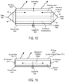
- FIG. 15 illustrates a side view of one embodiment of a cylindrically fed antenna structure.
- FIG. 16 illustrates another embodiment of the antenna system with an outgoing wave.
- FIG. 17 illustrates one embodiment of the placement of matrix drive circuitry with respect to antenna elements.
- FIG. 18 illustrates one embodiment of a TFT package.
- FIG. 19 is a block diagram of one embodiment of a communication system that performs dual reception simultaneously in a television system.
- FIG. 20 is a block diagram of another embodiment of a communication system having simultaneous transmit and receive paths.
- the RF choke assembly allows a glass-based radiating aperture to be coupled to the radial waveguide without a physical direct current (DC) electrical connection at the waveguide outer extents.
- DC direct current
- the use of the RF choke allows feeding an RF wave to a circular radiating aperture with a radial, edge fed waveguide over a broad range of RF frequencies as the RF energy is essentially trapped within the antenna at the outer edges of the radiating aperture and the waveguide.
- the radiating aperture can be substrates other than glass, including, but not limited to, sapphire, fused silicon, quartz, etc.
- the aperture may comprise a liquid crystal display (LCD).
- the RF choke assembly comprises one or more slots.
- the slots comprise milled (machined) slots.
- the slots may act as quarter wave transformers.
- the RF choke assembly comprises an electromagnetic band gap (EBG) choke.
- the EBG choke may be a printed circuit board (PCB)-based EBG choke.
- broadband launch and termination features that may be incorporated into an antenna.
- an antenna comprising a radial waveguide; an aperture operable to radiate radio frequency (RF) signals in response to an RF feed wave fed by the radial waveguide; and a radio frequency (RF) choke operable to block RF energy from exiting through a gap between outer portions of the waveguide and the aperture.
- RF radio frequency
- a slip plane located in proximity to the gap and facilitates potential movement of the waveguide and/or the radiating aperture.
- the waveguide comprises metal and the aperture comprises a glass or liquid crystal display (LCD) substrate, and the coefficient of thermal expansion of the waveguide and the aperture are different. Because they have different coefficients of thermal expansion, during operation of the antenna, heat may be generated that causes them to expand at different rates, which causes their placement with respect to each other to change positions, thereby preventing the waveguide and the radiating aperture from being connected to each other.
- LCD liquid crystal display
- the RF choke comprises one or more slots in the outer portion of the waveguide in the gap with each of the slots being used to block RF energy of a frequency band.
- the slots are part of a pair of rings in the outer portion of the waveguide. The rings are outside the active areas of the aperture used for radiating RF energy.
- the RF choke comprises an electromagnetic band gap (EBG) structure.
- EBG structure comprises a substrate with one or more vias.
- the substrate comprises a printed circuit board (PCB) with one or more electrically conductive patches and the one or more vias are plated with electrically conductive material.
- PCB is attached to the waveguide with conductive adhesive. Note that in one embodiment no vias are needed because the bandwidth is narrow.
- the aperture has a slotted array of antenna elements, wherein the slotted array comprises: a plurality of slots; and a plurality of patches, wherein each of the patches is co-located over and separated from a slot in the plurality of slots, forming a patch/slot pair, each patch/slot pair being turned off or on based on application of a voltage to the patch in the pair.
- the antenna elements are controlled and operable together to form a beam for a frequency band for use in holographic beam steering.
- FIGS. 2 and 3 illustrate a side view of one embodiment of an antenna with an RF choke assembly.
- antenna 200 includes a radial waveguide 201 , an aperture consisting of a substrate or glass layers (panels) 202 with antenna elements (not shown), a ground plane 203 , a dielectric (or other layer) transition 204 , an RF launch (feed) 205 and a termination 206 .
- glass layers 202 comprises two glass layers
- the radiating aperture comprises only one glass layer or other substrate with only one layer.
- the radiating aperture may comprises more than two layers that operate together to radiate RF energy (e.g., a beam).
- the aperture consisting of glass layers (substrate) 202 with antenna elements is operable to radiate radio frequency (RF) signals in response to an RF feed wave fed from RF launch 205 that travels from the central location of RF launch 205 along radial waveguide 201 around ground plane 203 (that acts as a guide plate) and 180° layer transition 210 to glass layers 202 to radiating aperture at the top portion of antenna 200 .
- RF radio frequency
- the antenna elements of glass layers 202 radiate RF energy.
- the RF energy radiated by glass layers in response to the RF energy from the feed wave is in the form of a beam.
- glass layers (or other substrate) 202 is manufactured using commercial television manufacturing techniques and does not have electrically conductive metal at the most external layer. This lack of conductive media on the external layer of the radiating aperture prevents a physical electrical connection between the subassemblies without further invasive processing of the subassemblies.
- an equivalent RF connection is made to prevent radiation from the connection seam.
- RF choke assembly 202 RF choke assembly RF choke 220 is operable to block RF energy from exiting through a gap between outer portions of waveguide 201 and glass layers 202 that form the radiating aperture.
- the difference in the coefficient of thermal expansion of glass layers 202 and feed structure material of waveguide 201 necessitates the need for an intermediate low-friction surface to ensure free planar expansion of the antenna media.
- the glass layers 202 forming the radiating aperture and waveguide housing are made of different materials with different coefficients of thermal expansion, there is some accommodation made at the extents of the housing of waveguide 201 to allow for physical movement as temperatures vary.
- the glass layers 202 are not permanently bonded to waveguide 201 .
- glass layers 202 are held mechanically in close intimate contact with waveguide 201 by clamping type features. That is, to hold glass layers 202 generally in position with respect to waveguide 201 in view of their differences in the coefficient of thermal expansion, a clamping mechanism is included.
- FIG. 4 illustrates an example of such a clamping mechanism. Referring to FIG. 4 , clamping machine 401 is coupled to a radome, which is over the glass layers 202 , and waveguide 201 .
- FIG. 2 illustrates an example of the slip plane location 211 .
- the material is thin film in nature and of a plastic material such as, for example, Acrylic, Acetate, or Polycarbonate and is adhered to the underside of the glass or top of the housing of waveguide 201 .
- a plastic material such as, for example, Acrylic, Acetate, or Polycarbonate
- the thin sheet material when attached to the glass provides some additional structural support and scratch resistance to the glass. The attachment may be made using an adhesive.
- the radial feed is designed such that each individual component can operate over a large bandwidth, i.e., >50%.
- the constituent components that make up the feed are: RF launch 205 , 180° layer transition 210 , termination 206 , intermediate ground plane 203 (guide-plate), the dielectric loading of dielectric transition 204 , and RF choke assembly 220 .
- RF launch 205 has a stepped transition from the input (co)axial mode (direction of propagation is through the conductor) to the radial mode (direction of propagation of the RF wave occurs from the edges of the conductor toward its center). This transition shorts the input pin to a capacitive step that compensates for the probe inductance, then impedance steps out to the full height of radial waveguide 201 .
- the number of steps needed to transition is related to the desired bandwidth of operation and the difference between the initial impedance of the launch and the final impedance of the guide. For example, in one embodiment, for a 10% change in bandwidth, a one step transition is used; for a 20% change in bandwidth, a two-step transition is used; and for a 50% change in bandwidth, a three (or more) step transition is used.
- Shorting the pin to ground plane 203 (the top plate of waveguide 201 ) allows for higher operating power levels by conducting generated heat away from the center pin of RF launch 205 into the housing of waveguide 201 which in one embodiment is metal (e.g., aluminum, copper, brass, gold, etc.). Any risk of dielectric breakdown is reduced by controlling the gaps between the stepped RF launch 205 and the bottom of the housing of waveguide 201 and breaking the sharp edges at the impedance steps.
- the top termination transition of RF launch 205 is designed in the same manner with impedance compensation added for the presence of the slow wave dielectric material. By designing the impedance transitions using discrete steps, RF launch 205 is easily manufactured using a three axis computer numeric control (CNC) end mil.
- CNC computer numeric control
- 180° layer transition 210 is accomplished in a similar manner to the launch and termination design.
- a chamfer or single step is used to compensate for the inductance of the 90 degree bends,
- multiple steps are used and can individually be tuned to accomplish a broadband match.
- the slow wave dielectric transition 204 of the top waveguide is placed at the top 90 degree bend thus adding asymmetry to the full 180 degree transition. This dielectric presence can be compensated for by adding asymmetry to the top and bottom transition steps.
- the equivalent RF grounding connection is accomplished by adding RF choke assembly 220 to the feed waveguide/glass interface such that the RF energy within the intended frequency band is reflected from RF choke assembly 220 interface without radiating into free space, and in-turn adding constructively with the propagating feed signal.
- these chokes are based on traditional waveguide choke flanges that help ensure robust RF connection for high power applications.
- Such chokes may also be based on electromagnetic band gap (EBG) structures as described in further detail below.
- ESG electromagnetic band gap
- RF choke assembly 220 includes waveguide style chokes having one or more slots, or channels, that are integrated into waveguide 201 .
- FIGS. 2 and 3 illustrates two slots. Note that in one embodiment as waveguide 201 is radial, the slots are actually rings that are inside the top of waveguide 201 . In one embodiment, the slots are designed to be placed at an odd integer multiple of a quarter wavelength (e.g., 1 ⁇ 4, 3 ⁇ 4, 5/4, etc.) from the inside of the RF feed junction (i.e., the outer most edge of the inner portion of waveguide 201 through which the feed wave propagates, shown as inner edge 250 in FIG. 2 ).
- a quarter wavelength e.g., 1 ⁇ 4, 3 ⁇ 4, 5/4, etc.
- the choke channels are also one quarter of a wavelength deep such that the reflected power is in phase at the top of the choke channel.
- the total phase length of the choke assembly will in turn be out of phase with the propagating feed signal, which gives the choke assembly (e.g., between the top and bottom of the slot(s)) the equivalent RF performance of an electrical short. This electrical short equivalence maintains the continuity of the feed structure walls without the need for a physical electrical connection.
- two choke slots may be used for each frequency band of the feed wave.
- two choke slots may be used for one receive frequency band while another two slots are used for a different receive frequency band or a transmit frequency band.
- transmit and receive frequency bands may be Ka transmit and receive frequency bands, respectively.
- the two receive frequency bands may be the Ka and Ku frequency bands, or any band in which communication occurs.
- the spacing of the slots is the same as above. That is, the slots would be designed to be placed at an odd integer multiple of a quarter wavelength (e.g., 1 ⁇ 4, 3 ⁇ 4, 5/4, etc.) from the inside of the RF feed junction (e.g., inner edge 250 ) to create a low impedance short.
- the slots of 1 ⁇ 4 ⁇ deep with a width sized for high impedance (where the ⁇ is that of the frequency to be blocked). While the each of the slots resonate at one frequency (to block energy at that frequency), the choke will likely block a band of frequencies. For example, while the slots resonates at one frequency of the ku band, the choke covers the entire ku band.
- FIG. 5 illustrates RF performance of the feed in FIG. 2 .
- the input return loss is better than 10 dB for more than 50% bandwidth.
- the antenna may include electromagnetic band gap (EBG) materials-based chokes.
- electromagnetic band gap (EBG) materials-based chokes are designed as unit cells that prevent propagation over specific frequency bands.
- the unit cells designed for separate frequency bands can be combined to provide multi-band or broadband operation.
- FIGS. 6 and 7 illustrate an example of an EBG unit cell choke.
- unit cell 600 comprises a printed circuit board (PCB) 601 with multiple vias, such as vias 602 A- 602 D. Depending on the thickness of the PCB board and the size of the vias, the via spacing may have to be adjusted.
- PCB printed circuit board
- Teflon, fiberglass or other materials may be used instead of a PCB.
- vias 602 A- 602 D are not filled and are electroplated with conductive plating, such as, for example, copper, aluminum, etc. Another material, such as, for example, n, may be deposited over the conductive plating for protection. In another alternative embodiment, vias 602 A- 602 D are filled with a material, such as, for example, epoxy.
- Each of vias 602 A- 602 D has an electrically conductive patch plated or attached over it, such as patches 603 A- 603 D, respectively.
- the patch and its via act as an LC resonator that looks like a short. Note that the patch is not required, and is not used in other embodiments.
- the four vias, vias 602 A- 602 D are used as an RF choke for two frequency bands.
- vias 602 A and 602 C operate as an RF choke for a transmit frequency band
- vias 602 B and 602 D operate as an RF choke for a receive frequency band. Note that both sets of two vias could be used for receive frequency bands or both for transmit frequency bands.
- FIG. 7 illustrates a side view of the EBG structure of FIG. 6 attached to a waveguide.
- PCB 601 is coupled to the waveguide using adhesive.
- the first via such as via 602 A, is aligned with the side of the waveguide.
- via 602 A is part of the choke for a transmit frequency band. Therefore, there is a slight overhang of PCB 601 over the inner side wall of the waveguide.
- one or more cushions may be between the EBG unit cell and the glass layers or substrate that operates as the radiating aperture.
- FIG. 8 illustrates a cylindrical feed with an EBG choke, such as the chokes shown in FIG. 7 .
- a via-free board is used and simplified assembly (since no conductive glue is needed).
- the techniques described above may be used with flat panel antennas. Embodiments of such flat panel antennas are disclosed.
- the flat panel antennas include one or more arrays of antenna elements on an antenna aperture.
- the antenna elements comprise liquid crystal cells.
- the flat panel antenna is a cylindrically fed antenna that includes matrix drive circuitry to uniquely address and drive each of the antenna elements that are not placed in rows and columns. Note that the feed need not be circular. In one embodiment, the elements are placed in rings.
- the antenna aperture having the one or more arrays of antenna elements is comprised of multiple segments coupled together. When coupled together, the combination of the segments form closed concentric rings of antenna elements. In one embodiment, the concentric rings are concentric with respect to the antenna feed.
- the flat panel antenna is part of a metamaterial antenna system.
- a metamaterial antenna system for communications satellite earth stations are described.
- the antenna system is a component or subsystem of a satellite earth station (ES) operating on a mobile platform (e.g., aeronautical, maritime, land, etc.) that operates using either Ka-band frequencies or Ku-band frequencies for civil commercial satellite communications.
- ES satellite earth station
- mobile platform e.g., aeronautical, maritime, land, etc.
- embodiments of the antenna system also can be used in earth stations that are not on mobile platforms (e.g., fixed or transportable earth stations).
- the antenna system uses surface scattering metamaterial technology to form and steer transmit and receive beams through separate antennas.
- the antenna systems are analog systems, in contrast to antenna systems that employ digital signal processing to electrically form and steer beams (such as phased array antennas).
- the antenna system is comprised of three functional subsystems: (1) a wave guiding structure consisting of a cylindrical wave feed architecture; (2) an array of wave scattering metamaterial unit cells that are part of antenna elements; and (3) a control structure to command formation of an adjustable radiation field (beam) from the metamaterial scattering elements using holographic principles.
- a wave guiding structure consisting of a cylindrical wave feed architecture
- an array of wave scattering metamaterial unit cells that are part of antenna elements
- a control structure to command formation of an adjustable radiation field (beam) from the metamaterial scattering elements using holographic principles.
- FIG. 9 illustrates a top view of one embodiment of a coaxial feed that is used to provide a cylindrical wave feed.
- the coaxial feed includes a center conductor and an outer conductor.
- the cylindrical wave feed architecture feeds the antenna from a central point with an excitation that spreads outward in a cylindrical manner from the feed point. That is, a cylindrically fed antenna creates an outward travelling concentric feed wave. Even so, the shape of the cylindrical feed antenna around the cylindrical feed can be circular, square or any shape.
- a cylindrically fed antenna creates an inward travelling feed wave. In such a case, the feed wave most naturally comes from a circular structure.
- FIG. 10 illustrates an aperture having one or more arrays of antenna elements placed in concentric rings around an input feed of the cylindrically fed antenna.
- the antenna elements comprise a group of patch antennas.
- This group of patch antennas comprises an array of scattering metamaterial elements.
- each scattering element in the antenna system is part of a unit cell that consists of a lower conductor, a dielectric substrate and an upper conductor that embeds a complementary electric inductive-capacitive resonator (“complementary electric LC” or “CELL”) that is etched in or deposited onto the upper conductor.
- complementary electric LC complementary electric inductive-capacitive resonator
- a liquid crystal is disposed in the gap around the scattering element. This LC is driven by the direct drive embodiments described above.
- liquid crystal is encapsulated in each unit cell and separates the lower conductor associated with a slot from an upper conductor associated with its patch.
- Liquid crystal has a permittivity that is a function of the orientation of the molecules comprising the liquid crystal, and the orientation of the molecules (and thus the permittivity) can be controlled by adjusting the bias voltage across the liquid crystal.
- the liquid crystal integrates an on/off switch for the transmission of energy from the guided wave to the CELC. When switched on, the CELC emits an electromagnetic wave like an electrically small dipole antenna. Note that the teachings herein are not limited to having a liquid crystal that operates in a binary fashion with respect to energy transmission.
- the feed geometry of this antenna system allows the antenna elements to be positioned at forty five degree)(45° angles to the vector of the wave in the wave feed. Note that other positions may be used (e.g., at 40° angles). This position of the elements enables control of the free space wave received by or transmitted/radiated from the elements.
- the antenna elements are arranged with an inter-element spacing that is less than a free-space wavelength of the operating frequency of the antenna. For example, if there are four scattering elements per wavelength, the elements in the 30 GHz transmit antenna will be approximately 2.5 mm (i.e., 1 ⁇ 4th the 10 mm free-space wavelength of 30 GHz).
- the two sets of elements are perpendicular to each other and simultaneously have equal amplitude excitation if controlled to the same tuning state. Rotating them +/ ⁇ 45 degrees relative to the feed wave excitation achieves both desired features at once. Rotating one set 0 degrees and the other 90 degrees would achieve the perpendicular goal, but not the equal amplitude excitation goal. Note that 0 and 90 degrees may be used to achieve isolation when feeding the array of antenna elements in a single structure from two sides.
- the amount of radiated power from each unit cell is controlled by applying a voltage to the patch (potential across the LC channel) using a controller. Traces to each patch are used to provide the voltage to the patch antenna. The voltage is used to tune or detune the capacitance and thus the resonance frequency of individual elements to effectuate beam forming. The voltage required is dependent on the liquid crystal mixture being used.
- the voltage tuning characteristic of liquid crystal mixtures is mainly described by a threshold voltage at which the liquid crystal starts to be affected by the voltage and the saturation voltage, above which an increase of the voltage does not cause major tuning in liquid crystal. These two characteristic parameters can change for different liquid crystal mixtures.
- a matrix drive is used to apply voltage to the patches in order to drive each cell separately from all the other cells without having a separate connection for each cell (direct drive). Because of the high density of elements, the matrix drive is an efficient way to address each cell individually.
- the control structure for the antenna system has 2 main components: the antenna array controller, which includes drive electronics, for the antenna system, is below the wave scattering structure, while the matrix drive switching array is interspersed throughout the radiating RF array in such a way as to not interfere with the radiation.
- the drive electronics for the antenna system comprise commercial off-the shelf LCD controls used in commercial television appliances that adjust the bias voltage for each scattering element by adjusting the amplitude or duty cycle of an AC bias signal to that element.
- the antenna array controller also contains a microprocessor executing the software.
- the control structure may also incorporate sensors (e.g., a GPS receiver, a three axis compass, a 3-axis accelerometer, 3-axis gyro, 3-axis magnetometer, etc.) to provide location and orientation information to the processor.
- sensors e.g., a GPS receiver, a three axis compass, a 3-axis accelerometer, 3-axis gyro, 3-axis magnetometer, etc.
- the location and orientation information may be provided to the processor by other systems in the earth station and/or may not be part of the antenna system.
- the antenna array controller controls which elements are turned off and those elements turned on and at which phase and amplitude level at the frequency of operation.
- the elements are selectively detuned for frequency operation by voltage application.
- a controller supplies an array of voltage signals to the RF patches to create a modulation, or control pattern.
- the control pattern causes the elements to be turned to different states.
- multistate control is used in which various elements are turned on and off to varying levels, further approximating a sinusoidal control pattern, as opposed to a square wave (i.e., a sinusoid gray shade modulation pattern).
- some elements radiate more strongly than others, rather than some elements radiate and some do not.
- Variable radiation is achieved by applying specific voltage levels, which adjusts the liquid crystal permittivity to varying amounts, thereby detuning elements variably and causing some elements to radiate more than others.
- the generation of a focused beam by the metamaterial array of elements can be explained by the phenomenon of constructive and destructive interference.
- Individual electromagnetic waves sum up (constructive interference) if they have the same phase when they meet in free space and waves cancel each other (destructive interference) if they are in opposite phase when they meet in free space.
- the slots in a slotted antenna are positioned so that each successive slot is positioned at a different distance from the excitation point of the guided wave, the scattered wave from that element will have a different phase than the scattered wave of the previous slot. If the slots are spaced one quarter of a guided wavelength apart, each slot will scatter a wave with a one fourth phase delay from the previous slot.
- the number of patterns of constructive and destructive interference that can be produced can be increased so that beams can be pointed theoretically in any direction plus or minus ninety degrees (90°)from the bore sight of the antenna array, using the principles of holography.
- the antenna can change the direction of the main beam.
- the time required to turn the unit cells on and off dictates the speed at which the beam can be switched from one location to another location.
- the antenna system produces one steerable beam for the uplink antenna and one steerable beam for the downlink antenna.
- the antenna system uses metamaterial technology to receive beams and to decode signals from the satellite and to form transmit beams that are directed toward the satellite.
- the antenna systems are analog systems, in contrast to antenna systems that employ digital signal processing to electrically form and steer beams (such as phased array antennas).
- the antenna system is considered a “surface” antenna that is planar and relatively low profile, especially when compared to conventional satellite dish receivers.
- FIG. 11 illustrates a perspective view of one row of antenna elements that includes a ground plane and a reconfigurable resonator layer.
- Reconfigurable resonator layer 1230 includes an array of tunable slots 1210 .
- the array of tunable slots 1210 can be configured to point the antenna in a desired direction.
- Each of the tunable slots can be tuned/adjusted by varying a voltage across the liquid crystal.
- Control module 1280 is coupled to reconfigurable resonator layer 1230 to modulate the array of tunable slots 1210 by varying the voltage across the liquid crystal in FIG. 11 .
- Control module 1280 may include a Field Programmable Gate Array (“FPGA”), a microprocessor, a controller, System-on-a-Chip (SoC), or other processing logic.
- control module 1280 includes logic circuitry (e.g., multiplexer) to drive the array of tunable slots 1210 .
- control module 1280 receives data that includes specifications for a holographic diffraction pattern to be driven onto the array of tunable slots 1210 .
- the holographic diffraction patterns may be generated in response to a spatial relationship between the antenna and a satellite so that the holographic diffraction pattern steers the downlink beams (and uplink beam if the antenna system performs transmit) in the appropriate direction for communication.
- a control module similar to control module 1280 may drive each array of tunable slots described in the figures of the disclosure.
- Radio Frequency (“RF”) holography is also possible using analogous techniques where a desired RF beam can be generated when an RF reference beam encounters an RF holographic diffraction pattern.
- the reference beam is in the form of a feed wave, such as feed wave 1205 (approximately 20 GHz in some embodiments).
- feed wave 1205 approximately 20 GHz in some embodiments.
- an interference pattern is calculated between the desired RF beam (the object beam) and the feed wave (the reference beam).
- the interference pattern is driven onto the array of tunable slots 1210 as a diffraction pattern so that the feed wave is “steered” into the desired RF beam (having the desired shape and direction).
- the feed wave encountering the holographic diffraction pattern “reconstructs” the object beam, which is formed according to design requirements of the communication system.
- FIG. 12 illustrates one embodiment of a tunable resonator/slot 1210 .
- Tunable slot 1210 includes an iris/slot 1212 , a radiating patch 1211 , and liquid crystal 1213 disposed between iris 1212 and patch 1211 .
- radiating patch 1211 is co-located with iris 1212 .
- FIG. 13 illustrates a cross section view of one embodiment of a physical antenna aperture.
- the antenna aperture includes ground plane 1245 , and a metal layer 1236 within iris layer 1233 , which is included in reconfigurable resonator layer 1230 .
- the antenna aperture of FIG. 13 includes a plurality of tunable resonator/slots 1210 of FIG. 12 .
- Iris/slot 1212 is defined by openings in metal layer 1236 .
- a feed wave such as feed wave 1205 of FIG. 11 , may have a microwave frequency compatible with satellite communication channels. The feed wave propagates between ground plane 1245 and resonator layer 1230 .
- Reconfigurable resonator layer 1230 also includes gasket layer 1232 and patch layer 1231 .
- Gasket layer 1232 is disposed below patch layer 1231 and iris layer 1233 .
- a spacer could replace gasket layer 1232 .
- iris layer 1233 is a printed circuit board (“PCB”) that includes a copper layer as metal layer 1236 .
- iris layer 1233 is glass. Iris layer 1233 may be other types of substrates.
- Openings may be etched in the copper layer to form slots 1212 .
- iris layer 1233 is conductively coupled by a conductive bonding layer to another structure (e.g., a waveguide) in FIG. 13 . Note that in an embodiment the iris layer is not conductively coupled by a conductive bonding layer and is instead interfaced with a non-conducting bonding layer.
- Patch layer 1231 may also be a PCB that includes metal as radiating patches 1211 .
- gasket layer 1232 includes spacers 1239 that provide a mechanical standoff to define the dimension between metal layer 1236 and patch 1211 .
- the spacers are 75 microns, but other sizes may be used (e.g., 3-200 mm).
- the antenna aperture of FIG. 13 includes multiple tunable resonator/slots, such as tunable resonator/slot 1210 includes patch 1211 , liquid crystal 1213 , and iris 1212 of FIG. 12 .
- the chamber for liquid crystal 1213 is defined by spacers 1239 , iris layer 1233 and metal layer 1236 . When the chamber is filled with liquid crystal, patch layer 1231 can be laminated onto spacers 1239 to seal liquid crystal within resonator layer 1230 .
- the resonant frequency of slot 1210 affects the energy radiated from feed wave 1205 propagating through the waveguide.
- the resonant frequency of a slot 1210 may be adjusted (by varying the capacitance) to 17 GHz so that the slot 1210 couples substantially no energy from feed wave 1205 .
- the resonant frequency of a slot 1210 may be adjusted to 20 GHz so that the slot 1210 couples energy from feed wave 1205 and radiates that energy into free space.
- the examples given are binary (fully radiating or not radiating at all), full gray scale control of the reactance, and therefore the resonant frequency of slot 1210 is possible with voltage variance over a multi-valued range.
- the energy radiated from each slot 1210 can be finely controlled so that detailed holographic diffraction patterns can be formed by the array of tunable slots.
- tunable slots in a row are spaced from each other by ⁇ /5. Other spacings may be used. In one embodiment, each tunable slot in a row is spaced from the closest tunable slot in an adjacent row by ⁇ /2, and, thus, commonly oriented tunable slots in different rows are spaced by ⁇ /4, though other spacings are possible (e.g., ⁇ /5, ⁇ /6.3). In another embodiment, each tunable slot in a row is spaced from the closest tunable slot in an adjacent row by ⁇ /3.
- Embodiments use reconfigurable metamaterial technology, such as described in U.S. patent application Ser. No. 14/550,178, entitled “Dynamic Polarization and Coupling Control from a Steerable Cylindrically Fed Holographic Antenna”, filed Nov. 21, 2014 and U.S. patent application Ser. No. 14/610,502, entitled “Ridged Waveguide Feed Structures for Reconfigurable Antenna”, filed Jan. 30, 2015.
- FIGS. 14A-D illustrate one embodiment of the different layers for creating the slotted array.
- the antenna array includes antenna elements that are positioned in rings, such as the example rings shown in FIG. 10 . Note that in this example the antenna array has two different types of antenna elements that are used for two different types of frequency bands.
- FIG. 14A illustrates a portion of the first iris board layer with locations corresponding to the slots.
- the circles are open areas/slots in the metallization in the bottom side of the iris substrate, and are for controlling the coupling of elements to the feed (the feed wave). Note that this layer is an optional layer and is not used in all designs.
- FIG. 14B illustrates a portion of the second iris board layer containing slots.
- FIG. 14C illustrates patches over a portion of the second iris board layer.
- FIG. 14D illustrates a top view of a portion of the slotted array.
- FIG. 15 illustrates a side view of one embodiment of a cylindrically fed antenna structure.
- the antenna produces an inwardly travelling wave using a double layer feed structure (i.e., two layers of a feed structure).
- the antenna includes a circular outer shape, though this is not required. That is, non-circular inward travelling structures can be used.
- the antenna structure in FIG. 15 includes the coaxial feed of FIG. 9 .
- a coaxial pin 1601 is used to excite the field on the lower level of the antenna.
- coaxial pin 1601 is a 50 ⁇ coax pin that is readily available.
- Coaxial pin 1601 is coupled (e.g., bolted) to the bottom of the antenna structure, which is conducting ground plane 1602 .
- interstitial conductor 1603 Separate from conducting ground plane 1602 is interstitial conductor 1603 , which is an internal conductor.
- conducting ground plane 1602 and interstitial conductor 1603 are parallel to each other.
- the distance between ground plane 1602 and interstitial conductor 1603 is 0.1-0.15′′. In another embodiment, this distance may be ⁇ /2, where ⁇ is the wavelength of the travelling wave at the frequency of operation.
- Ground plane 1602 is separated from interstitial conductor 1603 via a spacer 1604 .
- spacer 1604 is a foam or air-like spacer.
- spacer 1604 comprises a plastic spacer.
- dielectric layer 1605 On top of interstitial conductor 1603 is dielectric layer 1605 .
- dielectric layer 1605 is plastic.
- the purpose of dielectric layer 1605 is to slow the travelling wave relative to free space velocity. In one embodiment, dielectric layer 1605 slows the travelling wave by 30% relative to free space.
- the range of indices of refraction that are suitable for beam forming are 1.2-1.8, where free space has by definition an index of refraction equal to 1.
- Other dielectric spacer materials such as, for example, plastic, may be used to achieve this effect. Note that materials other than plastic may be used as long as they achieve the desired wave slowing effect.
- a material with distributed structures may be used as dielectric 1605 , such as periodic sub-wavelength metallic structures that can be machined or lithographically defined, for example.
- An RF-array 1606 is on top of dielectric 1605 .
- the distance between interstitial conductor 1603 and RF-array 606 is 0.1-0.15′′. In another embodiment, this distance may be ⁇ eff /2, where ⁇ eff is the effective wavelength in the medium at the design frequency.
- the antenna includes sides 1607 and 1608 .
- Sides 1607 and 1608 are angled to cause a travelling wave feed from coax pin 1601 to be propagated from the area below interstitial conductor 1603 (the spacer layer) to the area above interstitial conductor 1603 (the dielectric layer) via reflection.
- the angle of sides 1607 and 1608 are at 45° angles.
- sides 1607 and 1608 could be replaced with a continuous radius to achieve the reflection. While FIG. 15 shows angled sides that have angle of 45 degrees, other angles that accomplish signal transmission from lower level feed to upper level feed may be used.
- the 45° angles are replaced with a single step.
- the steps on one end of the antenna go around the dielectric layer, interstitial the conductor, and the spacer layer. The same two steps are at the other ends of these layers.
- the wave In operation, when a feed wave is fed in from coaxial pin 1601 , the wave travels outward concentrically oriented from coaxial pin 1601 in the area between ground plane 1602 and interstitial conductor 1603 .
- the concentrically outgoing waves are reflected by sides 1607 and 1608 and travel inwardly in the area between interstitial conductor 1603 and RF array 1606 .
- the reflection from the edge of the circular perimeter causes the wave to remain in phase (i.e., it is an in-phase reflection).
- the travelling wave is slowed by dielectric layer 1605 . At this point, the travelling wave starts interacting and exciting with elements in RF array 1606 to obtain the desired scattering.
- a termination 1609 is included in the antenna at the geometric center of the antenna.
- termination 1609 comprises a pin termination (e.g., a 50 ⁇ pin).
- termination 1609 comprises an RF absorber that terminates unused energy to prevent reflections of that unused energy back through the feed structure of the antenna. These could be used at the top of RF array 1606 .
- FIG. 16 illustrates another embodiment of the antenna system with an outgoing wave.
- two ground planes 1610 and 1611 are substantially parallel to each other with a dielectric layer 1612 (e.g., a plastic layer, etc.) in between ground planes.
- RF absorbers 1619 e.g., resistors
- a coaxial pin 1615 e.g., 50 ⁇ feeds the antenna.
- An RF array 1616 is on top of dielectric layer 1612 and ground plane 1611 .
- a feed wave is fed through coaxial pin 1615 and travels concentrically outward and interacts with the elements of RF array 1616 .
- the cylindrical feed in both the antennas of FIGS. 15 and 16 improves the service angle of the antenna.
- the antenna system has a service angle of seventy five degrees (75°) from the bore sight in all directions.
- the overall antenna gain is dependent on the gain of the constituent elements, which themselves are angle-dependent.
- the overall antenna gain typically decreases as the beam is pointed further off bore sight. At 75 degrees off bore sight, significant gain degradation of about 6 dB is expected.
- Embodiments of the antenna having a cylindrical feed solve one or more problems. These include dramatically simplifying the feed structure compared to antennas fed with a corporate divider network and therefore reducing total required antenna and antenna feed volume; decreasing sensitivity to manufacturing and control errors by maintaining high beam performance with coarser controls (extending all the way to simple binary control); giving a more advantageous side lobe pattern compared to rectilinear feeds because the cylindrically oriented feed waves result in spatially diverse side lobes in the far field; and allowing polarization to be dynamic, including allowing left-hand circular, right-hand circular, and linear polarizations, while not requiring a polarizer.
- RF array 1606 of FIG. 15 and RF array 1616 of FIG. 16 include a wave scattering subsystem that includes a group of patch antennas (i.e., scatterers) that act as radiators. This group of patch antennas comprises an array of scattering metamaterial elements.
- each scattering element in the antenna system is part of a unit cell that consists of a lower conductor, a dielectric substrate and an upper conductor that embeds a complementary electric inductive-capacitive resonator (“complementary electric LC” or “CELC”) that is etched in or deposited onto the upper conductor.
- a complementary electric inductive-capacitive resonator (“complementary electric LC” or “CELC”) that is etched in or deposited onto the upper conductor.
- a liquid crystal is injected in the gap around the scattering element.
- Liquid crystal is encapsulated in each unit cell and separates the lower conductor associated with a slot from an upper conductor associated with its patch.
- Liquid crystal has a permittivity that is a function of the orientation of the molecules comprising the liquid crystal, and the orientation of the molecules (and thus the permittivity) can be controlled by adjusting the bias voltage across the liquid crystal. Using this property, the liquid crystal acts as an on/off switch for the transmission of energy from the guided wave to the CELC. When switched on, the CELC emits an electromagnetic wave like an electrically small dipole antenna.
- Controlling the thickness of the LC increases the beam switching speed.
- a fifty percent (50%) reduction in the gap between the lower and the upper conductor results in a fourfold increase in speed.
- the thickness of the liquid crystal results in a beam switching speed of approximately fourteen milliseconds (14 ms).
- the LC is doped in a manner well-known in the art to improve responsiveness so that a seven millisecond (7 ms) requirement can be met.
- the CELC element is responsive to a magnetic field that is applied parallel to the plane of the CELC element and perpendicular to the CELC gap complement.
- a voltage is applied to the liquid crystal in the metamaterial scattering unit cell, the magnetic field component of the guided wave induces a magnetic excitation of the CELC, which, in turn, produces an electromagnetic wave in the same frequency as the guided wave.
- the phase of the electromagnetic wave generated by a single CELC can be selected by the position of the CELC on the vector of the guided wave.
- Each cell generates a wave in phase with the guided wave parallel to the CELC. Because the CELCs are smaller than the wave length, the output wave has the same phase as the phase of the guided wave as it passes beneath the CELC.
- the cylindrical feed geometry of this antenna system allows the CELC elements to be positioned at forty five degree (45°) angles to the vector of the wave in the wave feed. This position of the elements enables control of the polarization of the free space wave generated from or received by the elements.
- the CELCs are arranged with an inter-element spacing that is less than a free-space wavelength of the operating frequency of the antenna. For example, if there are four scattering elements per wavelength, the elements in the 30 GHz transmit antenna will be approximately 2.5 mm (i.e., 1 ⁇ 4th the 10 mm free-space wavelength of 30 GHz).
- the CELCs are implemented with patch antennas that include a patch co-located over a slot with liquid crystal between the two.
- the metamaterial antenna acts like a slotted (scattering) wave guide. With a slotted wave guide, the phase of the output wave depends on the location of the slot in relation to the guided wave.
- the antenna elements are placed on the cylindrical feed antenna aperture in a way that allows for a systematic matrix drive circuit.
- the placement of the cells includes placement of the transistors for the matrix drive.
- FIG. 17 illustrates one embodiment of the placement of matrix drive circuitry with respect to antenna elements.
- row controller 1701 is coupled to transistors 1711 and 1712 , via row select signals Row 1 and Row 2 , respectively, and column controller 1702 is coupled to transistors 1711 and 1712 via column select signal Column1.
- Transistor 1711 is also coupled to antenna element 1721 via connection to patch 1731
- transistor 1712 is coupled to antenna element 1722 via connection to patch 1732 .
- the cells are placed on concentric rings and each of the cells is connected to a transistor that is placed beside the cell and acts as a switch to drive each cell separately.
- the matrix drive circuitry is built in order to connect every transistor with a unique address as the matrix drive approach requires. Because the matrix drive circuit is built by row and column traces (similar to LCDs) but the cells are placed on rings, there is no systematic way to assign a unique address to each transistor. This mapping problem results in very complex circuitry to cover all the transistors and leads to a significant increase in the number of physical traces to accomplish the routing. Because of the high density of cells, those traces disturb the RF performance of the antenna due to coupling effect. Also, due to the complexity of traces and high packing density, the routing of the traces cannot be accomplished by commercially available layout tools.
- the matrix drive circuitry is predefined before the cells and transistors are placed. This ensures a minimum number of traces that are necessary to drive all the cells, each with a unique address. This strategy reduces the complexity of the drive circuitry and simplifies the routing, which subsequently improves the RF performance of the antenna.
- the cells are placed on a regular rectangular grid composed of rows and columns that describe the unique address of each cell.
- the cells are grouped and transformed to concentric circles while maintaining their address and connection to the rows and columns as defined in the first step.
- a goal of this transformation is not only to put the cells on rings but also to keep the distance between cells and the distance between rings constant over the entire aperture. In order to accomplish this goal, there are several ways to group the cells.
- a TFT package is used to enable placement and unique addressing in the matrix drive.
- FIG. 18 illustrates one embodiment of a TFT package. Referring to FIG. 18 , a TFT and a hold capacitor 1803 is shown with input and output ports. There are two input ports connected to traces 1801 and two output ports connected to traces 1802 to connect the TFTs together using the rows and columns. In one embodiment, the row and column traces cross in 90° angles to reduce, and potentially minimize, the coupling between the row and column traces. In one embodiment, the row and column traces are on different layers.
- the combined antenna apertures are used in a television system that operates in conjunction with a set top box.
- satellite signals received by the antenna are provided to a set top box (e.g., a DirecTV receiver) of a television system.
- the combined antenna operation is able to simultaneously receive RF signals at two different frequencies and/or polarizations. That is, one sub-array of elements is controlled to receive RF signals at one frequency and/or polarization, while another sub-array is controlled to receive signals at another, different frequency and/or polarization. These differences in frequency or polarization represent different channels being received by the television system.
- the two antenna arrays can be controlled for two different beam positions to receive channels from two different locations (e.g., two different satellites) to simultaneously receive multiple channels.
- FIG. 19 is a block diagram of one embodiment of a communication system that performs dual reception simultaneously in a television system.
- antenna 1401 includes two spatially interleaved antenna apertures operable independently to perform dual reception simultaneously at different frequencies and/or polarizations as described above. Note that while only two spatially interleaved antenna operations are mentioned, the TV system may have more than two antenna apertures (e.g., 3, 4, 5, etc. antenna apertures).
- antenna 1401 is coupled to diplexer 1430 .
- the coupling may include one or more feeding networks that receive the signals from elements of the two slotted arrays to produce two signals that are fed into diplexer 1430 .
- diplexer 1430 is a commercially available diplexer (e.g., model PB1081WA Ku-band sitcom diplexor from A1 Microwave).
- Diplexer 1430 is coupled to a pair of low noise block down converters (LNBs) 1426 and 1427 , which perform a noise filtering function, a down conversion function, and amplification in a manner well-known in the art.
- LNBs 1426 and 1427 are in an out-door unit (ODU).
- ODU out-door unit
- LNBs 1426 and 1427 are integrated into the antenna apparatus.
- LNBs 1426 and 1427 are coupled to a set top box 1402 , which is coupled to television 1403 .
- Set top box 1402 includes a pair of analog-to-digital converters (ADCs) 1421 and 1422 , which are coupled to LNBs 1426 and 1427 , to convert the two signals output from diplexer 1430 into digital format.
- ADCs analog-to-digital converters
- the signals are demodulated by demodulator 1423 and decoded by decoder 1424 to obtain the encoded data on the received waves.
- the decoded data is then sent to controller 1425 , which sends it to television 1403 .
- Controller 1450 controls antenna 1401 , including the interleaved slotted array elements of both antenna apertures on the single combined physical aperture.
- FIG. 20 is a block diagram of another embodiment of a communication system having simultaneous transmit and receive paths. While only one transmit path and one receive path are shown, the communication system may include more than one transmit path and/or more than one receive path.
- antenna 1401 includes two spatially interleaved antenna arrays operable independently to transmit and receive simultaneously at different frequencies as described above.
- antenna 1401 is coupled to diplexer 1445 .
- the coupling may be by one or more feeding networks.
- diplexer 1445 combines the two signals and the connection between antenna 1401 and diplexer 1445 is a single broad-band feeding network that can carry both frequencies.
- Diplexer 1445 is coupled to a low noise block down converter (LNBs) 1427 , which performs a noise filtering function and a down conversion and amplification function in a manner well-known in the art.
- LNB 1427 is in an out-door unit (ODU).
- ODU out-door unit
- LNB 1427 is integrated into the antenna apparatus.
- LNB 1427 is coupled to a modem 1460 , which is coupled to computing system 1440 (e.g., a computer system, modem, etc.).
- Modem 1460 includes an analog-to-digital converter (ADC) 1422 , which is coupled to LNB 1427 , to convert the received signal output from diplexer 1445 into digital format. Once converted to digital format, the signal is demodulated by demodulator 1423 and decoded by decoder 1424 to obtain the encoded data on the received wave. The decoded data is then sent to controller 1425 , which sends it to computing system 1440 .
- ADC analog-to-digital converter
- Modem 1460 also includes an encoder 1430 that encodes data to be transmitted from computing system 1440 .
- the encoded data is modulated by modulator 1431 and then converted to analog by digital-to-analog converter (DAC) 1432 .
- DAC digital-to-analog converter
- the analog signal is then filtered by a BUC (up-convert and high pass amplifier) 1433 and provided to one port of diplexer 1445 .
- BUC 1433 is in an out-door unit (ODU).
- Diplexer 1445 operating in a manner well-known in the art provides the transmit signal to antenna 1401 for transmission.
- Controller 1450 controls antenna 1401 , including the two arrays of antenna elements on the single combined physical aperture.
- the full duplex communication system shown in FIG. 20 has a number of applications, including but not limited to, internet communication, vehicle communication (including software updating), etc.
- the present invention also relates to apparatus for performing the operations herein.
- This apparatus may be specially constructed for the required purposes, or it may comprise a general purpose computer selectively activated or reconfigured by a computer program stored in the computer.
- a computer program may be stored in a computer readable storage medium, such as, but is not limited to, any type of disk including floppy disks, optical disks, CD-ROMs, and magnetic-optical disks, read-only memories (ROMs), random access memories (RAMs), EPROMs, EEPROMs, magnetic or optical cards, or any type of media suitable for storing electronic instructions, and each coupled to a computer system bus.
- a machine-readable medium includes any mechanism for storing or transmitting information in a form readable by a machine (e.g., a computer).
- a machine-readable medium includes read only memory (“ROM”); random access memory (“RAM”); magnetic disk storage media; optical storage media; flash memory devices; etc.
Landscapes
- Variable-Direction Aerials And Aerial Arrays (AREA)
- Waveguide Aerials (AREA)
- Details Of Aerials (AREA)
- Aerials With Secondary Devices (AREA)
Abstract
Description
Claims (28)
Priority Applications (8)
| Application Number | Priority Date | Filing Date | Title |
|---|---|---|---|
| US15/442,320 US10811784B2 (en) | 2016-03-01 | 2017-02-24 | Broadband RF radial waveguide feed with integrated glass transition |
| JP2018545813A JP6913690B2 (en) | 2016-03-01 | 2017-02-27 | Wideband RF radial waveguide feeding section with integrated glass transition |
| CN201780014723.9A CN108713276B (en) | 2016-03-01 | 2017-02-27 | Antenna with broadband RF radial waveguide feed |
| PCT/US2017/019743 WO2017151520A1 (en) | 2016-03-01 | 2017-02-27 | Broadband rf radial waveguide feed with integrated glass transition |
| ES17711403T ES2874634T3 (en) | 2016-03-01 | 2017-02-27 | Wideband RF radial waveguide feed with integrated glass transcription |
| KR1020187027301A KR102272577B1 (en) | 2016-03-01 | 2017-02-27 | Broadband RF radial waveguide feed with integrated glass transition |
| EP17711403.0A EP3424105B1 (en) | 2016-03-01 | 2017-02-27 | Broadband rf radial waveguide feed with integrated glass transition |
| IL261334A IL261334B (en) | 2016-03-01 | 2018-08-23 | Broadband rf radial waveguide feed with integrated glass transition |
Applications Claiming Priority (2)
| Application Number | Priority Date | Filing Date | Title |
|---|---|---|---|
| US201662302042P | 2016-03-01 | 2016-03-01 | |
| US15/442,320 US10811784B2 (en) | 2016-03-01 | 2017-02-24 | Broadband RF radial waveguide feed with integrated glass transition |
Publications (2)
| Publication Number | Publication Date |
|---|---|
| US20170256865A1 US20170256865A1 (en) | 2017-09-07 |
| US10811784B2 true US10811784B2 (en) | 2020-10-20 |
Family
ID=59722334
Family Applications (1)
| Application Number | Title | Priority Date | Filing Date |
|---|---|---|---|
| US15/442,320 Active 2038-08-07 US10811784B2 (en) | 2016-03-01 | 2017-02-24 | Broadband RF radial waveguide feed with integrated glass transition |
Country Status (8)
| Country | Link |
|---|---|
| US (1) | US10811784B2 (en) |
| EP (1) | EP3424105B1 (en) |
| JP (1) | JP6913690B2 (en) |
| KR (1) | KR102272577B1 (en) |
| CN (1) | CN108713276B (en) |
| ES (1) | ES2874634T3 (en) |
| IL (1) | IL261334B (en) |
| WO (1) | WO2017151520A1 (en) |
Cited By (7)
| Publication number | Priority date | Publication date | Assignee | Title |
|---|---|---|---|---|
| US20210273311A1 (en) * | 2020-05-19 | 2021-09-02 | Kymeta Corporation | Expansion compensation structure for an antenna |
| US11322843B2 (en) * | 2016-09-14 | 2022-05-03 | Kymeta Corporation | Impedance matching for an aperture antenna |
| US20220239000A1 (en) * | 2019-04-12 | 2022-07-28 | Kymeta Corporation | Non-circular center-fed antenna and method for using the same |
| US11489258B2 (en) * | 2018-01-17 | 2022-11-01 | Kymeta Corporation | Broad tunable bandwidth radial line slot antenna |
| US11569584B2 (en) * | 2016-11-03 | 2023-01-31 | Kymeta Corporation | Directional coupler feed for flat panel antennas |
| US20230238711A1 (en) * | 2019-12-30 | 2023-07-27 | Kymeta Corporation | Multiband guiding structures for antennas |
| US20230344118A1 (en) * | 2021-03-23 | 2023-10-26 | Beijing Boe Technology Development Co., Ltd. | Antenna Unit, Preparation Method Therefor, and Electronic Device |
Families Citing this family (25)
| Publication number | Priority date | Publication date | Assignee | Title |
|---|---|---|---|---|
| US9490540B1 (en) * | 2015-09-02 | 2016-11-08 | Hand Held Products, Inc. | Patch antenna |
| CN109314145B (en) * | 2016-06-09 | 2021-07-13 | 夏普株式会社 | TFT substrate, scanning antenna including TFT substrate, and method of manufacturing TFT substrate |
| US10903572B2 (en) * | 2016-10-24 | 2021-01-26 | Kymeta Corporation | Dual resonator for flat panel antennas |
| CN110998965B (en) * | 2017-08-09 | 2021-09-07 | 夏普株式会社 | Scanning antenna and manufacturing method of scanning antenna |
| US20190103681A1 (en) * | 2017-10-04 | 2019-04-04 | Kymeta Corporation | Feed lamination tool |
| DE112019000636B4 (en) * | 2018-02-02 | 2025-10-16 | AGC Inc. | Antenna device, window pane for a vehicle and window pane structure |
| US11139695B2 (en) | 2018-02-12 | 2021-10-05 | Ossia Inc. | Flat panel substrate with integrated antennas and wireless power transmission system |
| US20200044326A1 (en) * | 2018-08-03 | 2020-02-06 | Kymeta Corporation | Composite stack-up for flat panel metamaterial antenna |
| CN109462027B (en) * | 2018-12-21 | 2023-05-26 | 中国电子科技集团公司第五十四研究所 | A method of manufacturing a waveguide slot radiation unit |
| SE542733C2 (en) * | 2019-02-08 | 2020-06-30 | Gapwaves Ab | Antenna array based on one or more metamaterial structures |
| JP7599428B2 (en) * | 2019-03-08 | 2024-12-13 | アプライド マテリアルズ インコーポレイテッド | Chucking process and system for a substrate processing chamber - Patents.com |
| CN110061348B (en) * | 2019-04-04 | 2020-08-11 | 东南大学 | A Radial Multi-Beam Gap Waveguide Slot Antenna Array Applied in Microwave Section |
| CN111697341B (en) * | 2020-06-28 | 2023-08-25 | 京东方科技集团股份有限公司 | Slit antenna and communication device |
| US11394429B2 (en) | 2020-12-02 | 2022-07-19 | Dupont Electronics, Inc. | Panel having integrated antennas for enhancing range of telecommunication signal transmissions inside buildings |
| US12401136B2 (en) * | 2020-12-22 | 2025-08-26 | A.D.S. International S.R.L. | Antenna and antenna system for satellite communications |
| CN112366447B (en) * | 2021-01-13 | 2021-04-02 | 成都天锐星通科技有限公司 | Antenna unit and antenna unit manufacturing method |
| CN114824766B (en) * | 2021-01-19 | 2023-05-26 | 大唐移动通信设备有限公司 | Multi-mode navigation antenna |
| KR102411398B1 (en) * | 2021-02-23 | 2022-06-22 | 한국해양대학교 산학협력단 | High gain antenna for radar system for monitoring coastline erosion environment |
| CN113258305B (en) * | 2021-04-30 | 2022-07-29 | 西南电子技术研究所(中国电子科技集团公司第十研究所) | Method for preparing high-frequency liquid crystal radiation area subarray of electric control holographic antenna |
| US11784413B2 (en) * | 2021-06-12 | 2023-10-10 | The Johns Hopkins University | Wideband radial line slot array antenna |
| US12176616B2 (en) * | 2021-08-13 | 2024-12-24 | Kymeta Corporation | Dual beam launcher |
| CN113970562B (en) * | 2021-08-30 | 2023-08-29 | 杭州电子科技大学 | Microwave/millimeter wave waveguide sensor with filtering function |
| US12438281B2 (en) * | 2021-11-19 | 2025-10-07 | Sderotech, Inc. | Variable dielectric based antenna with improved response time |
| WO2025206802A1 (en) * | 2024-03-29 | 2025-10-02 | 주식회사 에이피알 | Antenna device |
| WO2025206801A1 (en) * | 2024-03-29 | 2025-10-02 | 주식회사 에이피알 | Antenna device |
Citations (12)
| Publication number | Priority date | Publication date | Assignee | Title |
|---|---|---|---|---|
| DE4026432A1 (en) | 1989-08-21 | 1991-02-28 | Radial Antenna Lab Ltd | PLANAR ANTENNA |
| EP1122813A2 (en) | 2000-02-04 | 2001-08-08 | Hughes Electronics Corporation | An improved phased array terminal for equatorial satellite constellations |
| EP1229342A2 (en) | 2001-01-31 | 2002-08-07 | Qinetiq Limited | Signal detection using a phased array antenna |
| US20040233117A1 (en) | 2003-05-23 | 2004-11-25 | Milroy William W. | Variable inclination continuous transverse stub array |
| US7009558B1 (en) | 2005-03-14 | 2006-03-07 | Delphi Technologies, Inc. | Vehicle mounted satellite tracking system |
| EP1863114A1 (en) | 2006-06-01 | 2007-12-05 | BSH Bosch und Siemens Hausgeräte GmbH | Electromagnetic bandgap seal for microwave energy |
| US20080068263A1 (en) | 2006-09-19 | 2008-03-20 | Tekawy Jonathan A | Method and system for attitude determination of a platform using global navigation satellite system and a steered antenna |
| WO2013134585A2 (en) | 2012-03-09 | 2013-09-12 | Viasat, Inc. | Aperiodic phased array antenna with single bit phase shifters |
| US20150236412A1 (en) | 2014-02-19 | 2015-08-20 | Adam Bily | Dynamic polarization and coupling control from a steerable cylindrically fed holographic antenna |
| US20150288063A1 (en) * | 2014-04-07 | 2015-10-08 | Mikala C. Johnson | Beam shaping for reconfigurable holographic antennas |
| US20150380789A1 (en) * | 2013-02-15 | 2015-12-31 | Technische Universität Darmstadt | Phase shift device |
| US20160006121A1 (en) | 2014-07-07 | 2016-01-07 | Qatar Foundation For Education, Science And Community Development | Reconfigurable radio direction finder system and method |
Family Cites Families (13)
| Publication number | Priority date | Publication date | Assignee | Title |
|---|---|---|---|---|
| US4647940A (en) * | 1982-09-27 | 1987-03-03 | Rogers Corporation | Parallel plate waveguide antenna |
| US5049895A (en) * | 1985-01-24 | 1991-09-17 | Yoshiharu Ito | Flat circular waveguide device |
| JPH03219706A (en) * | 1989-11-30 | 1991-09-27 | Rajiaru Antenna Kenkyusho:Kk | Planer antenna |
| JPH07202557A (en) * | 1993-12-28 | 1995-08-04 | Toshiba Corp | Radial waveguide beam tilt antenna device |
| US6201508B1 (en) * | 1999-12-13 | 2001-03-13 | Space Systems/Loral, Inc. | Injection-molded phased array antenna system |
| FR2843833B1 (en) * | 2002-08-23 | 2004-10-01 | Thomson Licensing Sa | RLSA ANTENNA WITH DOUBLE ORTHOGONAL LINEAR POLARIZATIONS |
| JP2007166115A (en) * | 2005-12-12 | 2007-06-28 | Matsushita Electric Ind Co Ltd | Antenna device |
| EP2343774A4 (en) * | 2008-10-29 | 2013-11-27 | Panasonic Corp | HIGH FREQUENCY WAVEGUIDE AND PHASE - LESS USING RADIATOR, ELECTRONIC DEVICE USING THE PHASE - DISPENSER AND RADIATOR, ANTENNA DEVICE, AND ELECTRONIC DEVICE EQUIPPED WITH SAME |
| CN103326126A (en) * | 2012-03-20 | 2013-09-25 | 西门子公司 | Leaking transmission wire and MIMO communication system based on same |
| CN103904408B (en) * | 2014-03-11 | 2016-08-31 | 西安电子科技大学昆山创新研究院 | Stable phase angle center measurement type antenna |
| US9490535B2 (en) * | 2014-06-30 | 2016-11-08 | Huawei Technologies Co., Ltd. | Apparatus and assembling method of a dual polarized agile cylindrical antenna array with reconfigurable radial waveguides |
| CN104600419B (en) * | 2015-01-05 | 2018-11-06 | 北京邮电大学 | Radial line Fed Dielectric Resonator aerial array |
| CN105006631B (en) * | 2015-07-24 | 2017-11-03 | 哈尔滨工业大学 | Automatically controlled zero scan wave guide wave leakage antenna excessively based on liquid crystal |
-
2017
- 2017-02-24 US US15/442,320 patent/US10811784B2/en active Active
- 2017-02-27 KR KR1020187027301A patent/KR102272577B1/en active Active
- 2017-02-27 EP EP17711403.0A patent/EP3424105B1/en active Active
- 2017-02-27 JP JP2018545813A patent/JP6913690B2/en active Active
- 2017-02-27 ES ES17711403T patent/ES2874634T3/en active Active
- 2017-02-27 CN CN201780014723.9A patent/CN108713276B/en not_active Expired - Fee Related
- 2017-02-27 WO PCT/US2017/019743 patent/WO2017151520A1/en not_active Ceased
-
2018
- 2018-08-23 IL IL261334A patent/IL261334B/en unknown
Patent Citations (12)
| Publication number | Priority date | Publication date | Assignee | Title |
|---|---|---|---|---|
| DE4026432A1 (en) | 1989-08-21 | 1991-02-28 | Radial Antenna Lab Ltd | PLANAR ANTENNA |
| EP1122813A2 (en) | 2000-02-04 | 2001-08-08 | Hughes Electronics Corporation | An improved phased array terminal for equatorial satellite constellations |
| EP1229342A2 (en) | 2001-01-31 | 2002-08-07 | Qinetiq Limited | Signal detection using a phased array antenna |
| US20040233117A1 (en) | 2003-05-23 | 2004-11-25 | Milroy William W. | Variable inclination continuous transverse stub array |
| US7009558B1 (en) | 2005-03-14 | 2006-03-07 | Delphi Technologies, Inc. | Vehicle mounted satellite tracking system |
| EP1863114A1 (en) | 2006-06-01 | 2007-12-05 | BSH Bosch und Siemens Hausgeräte GmbH | Electromagnetic bandgap seal for microwave energy |
| US20080068263A1 (en) | 2006-09-19 | 2008-03-20 | Tekawy Jonathan A | Method and system for attitude determination of a platform using global navigation satellite system and a steered antenna |
| WO2013134585A2 (en) | 2012-03-09 | 2013-09-12 | Viasat, Inc. | Aperiodic phased array antenna with single bit phase shifters |
| US20150380789A1 (en) * | 2013-02-15 | 2015-12-31 | Technische Universität Darmstadt | Phase shift device |
| US20150236412A1 (en) | 2014-02-19 | 2015-08-20 | Adam Bily | Dynamic polarization and coupling control from a steerable cylindrically fed holographic antenna |
| US20150288063A1 (en) * | 2014-04-07 | 2015-10-08 | Mikala C. Johnson | Beam shaping for reconfigurable holographic antennas |
| US20160006121A1 (en) | 2014-07-07 | 2016-01-07 | Qatar Foundation For Education, Science And Community Development | Reconfigurable radio direction finder system and method |
Non-Patent Citations (4)
| Title |
|---|
| International Preliminary Report on Patentability received for PCT Patent Application No. PCT/US2017/019743, dated Sep. 13, 2018, 10 pages. |
| International Preliminary Report on Patentability received for PCT Patent Application No. PCT/US2017/020232, dated Sep. 13, 2018, 11 pages. |
| International Search Report and Written Opinion received for PCT Patent Application No. PCT/US2017/020232, dated Jun. 20, 2017, 13 pages. |
| PCT Application No. PCT/US2017/019743, International Search Report and the Written Opinion, dated May 31, 2017, 15 pgs. |
Cited By (14)
| Publication number | Priority date | Publication date | Assignee | Title |
|---|---|---|---|---|
| US11322843B2 (en) * | 2016-09-14 | 2022-05-03 | Kymeta Corporation | Impedance matching for an aperture antenna |
| US11569584B2 (en) * | 2016-11-03 | 2023-01-31 | Kymeta Corporation | Directional coupler feed for flat panel antennas |
| US12027785B2 (en) | 2018-01-17 | 2024-07-02 | Kymeta Corporation | Broad tunable bandwidth radial line slot antenna |
| US11489258B2 (en) * | 2018-01-17 | 2022-11-01 | Kymeta Corporation | Broad tunable bandwidth radial line slot antenna |
| US12542354B1 (en) | 2018-01-17 | 2026-02-03 | Kymeta Corporation | Broad tunable bandwidth radial line slot antenna |
| US20220239000A1 (en) * | 2019-04-12 | 2022-07-28 | Kymeta Corporation | Non-circular center-fed antenna and method for using the same |
| US11670858B2 (en) * | 2019-04-12 | 2023-06-06 | Kymeta Corporation | Non-circular center-fed antenna and method for using the same |
| US20230238711A1 (en) * | 2019-12-30 | 2023-07-27 | Kymeta Corporation | Multiband guiding structures for antennas |
| US11799211B2 (en) * | 2019-12-30 | 2023-10-24 | Kymeta Corporation | Multiband guiding structures for antennas |
| US11909091B2 (en) * | 2020-05-19 | 2024-02-20 | Kymeta Corporation | Expansion compensation structure for an antenna |
| US20240258677A1 (en) * | 2020-05-19 | 2024-08-01 | Kymeta Corporation | Expansion compensation structure for an antenna |
| US20210273311A1 (en) * | 2020-05-19 | 2021-09-02 | Kymeta Corporation | Expansion compensation structure for an antenna |
| US20230344118A1 (en) * | 2021-03-23 | 2023-10-26 | Beijing Boe Technology Development Co., Ltd. | Antenna Unit, Preparation Method Therefor, and Electronic Device |
| US12068534B2 (en) * | 2021-03-23 | 2024-08-20 | Beijing Boe Technology Development Co., Ltd. | Antenna unit, preparation method therefor, and electronic device |
Also Published As
| Publication number | Publication date |
|---|---|
| CN108713276A (en) | 2018-10-26 |
| KR102272577B1 (en) | 2021-07-06 |
| US20170256865A1 (en) | 2017-09-07 |
| WO2017151520A1 (en) | 2017-09-08 |
| EP3424105A1 (en) | 2019-01-09 |
| JP6913690B2 (en) | 2021-08-04 |
| ES2874634T3 (en) | 2021-11-05 |
| IL261334B (en) | 2022-01-01 |
| IL261334A (en) | 2018-10-31 |
| JP2019507556A (en) | 2019-03-14 |
| CN108713276B (en) | 2021-11-19 |
| EP3424105B1 (en) | 2021-04-07 |
| KR20180121549A (en) | 2018-11-07 |
Similar Documents
| Publication | Publication Date | Title |
|---|---|---|
| US10811784B2 (en) | Broadband RF radial waveguide feed with integrated glass transition | |
| US20220328962A1 (en) | Impedance matching for an aperture antenna | |
| US12542354B1 (en) | Broad tunable bandwidth radial line slot antenna | |
| US10547097B2 (en) | Antenna aperture with clamping mechanism | |
| US11700054B2 (en) | Modular metasurface antenna with high instantaneous bandwidth | |
| US11049658B2 (en) | Storage capacitor for use in an antenna aperture | |
| US20190089065A1 (en) | Apparatus with rectangular waveguide to radial mode transition | |
| EP4154356A1 (en) | Single-layer wide angle impedance matching (waim) | |
| US20190097299A1 (en) | Integrated transceiver for antenna systems | |
| US11799211B2 (en) | Multiband guiding structures for antennas | |
| US11670858B2 (en) | Non-circular center-fed antenna and method for using the same |
Legal Events
| Date | Code | Title | Description |
|---|---|---|---|
| AS | Assignment |
Owner name: KYMETA CORPORATION, WASHINGTON Free format text: ASSIGNMENT OF ASSIGNORS INTEREST;ASSIGNORS:SIKES, BENJAMIN;SAZEGAR, MOHSEN;MOREY, ROBERT;AND OTHERS;SIGNING DATES FROM 20170227 TO 20170308;REEL/FRAME:041585/0487 |
|
| STPP | Information on status: patent application and granting procedure in general |
Free format text: DOCKETED NEW CASE - READY FOR EXAMINATION |
|
| STPP | Information on status: patent application and granting procedure in general |
Free format text: NON FINAL ACTION MAILED |
|
| STPP | Information on status: patent application and granting procedure in general |
Free format text: RESPONSE TO NON-FINAL OFFICE ACTION ENTERED AND FORWARDED TO EXAMINER |
|
| STPP | Information on status: patent application and granting procedure in general |
Free format text: FINAL REJECTION MAILED |
|
| STPP | Information on status: patent application and granting procedure in general |
Free format text: NOTICE OF ALLOWANCE MAILED -- APPLICATION RECEIVED IN OFFICE OF PUBLICATIONS |
|
| STPP | Information on status: patent application and granting procedure in general |
Free format text: PUBLICATIONS -- ISSUE FEE PAYMENT RECEIVED |
|
| STCF | Information on status: patent grant |
Free format text: PATENTED CASE |
|
| MAFP | Maintenance fee payment |
Free format text: PAYMENT OF MAINTENANCE FEE, 4TH YR, SMALL ENTITY (ORIGINAL EVENT CODE: M2551); ENTITY STATUS OF PATENT OWNER: SMALL ENTITY Year of fee payment: 4 |
|
| AS | Assignment |
Owner name: TRINITY CAPITAL INC., ARIZONA Free format text: SECURITY INTEREST;ASSIGNOR:KYMETA CORPORATION;REEL/FRAME:068276/0105 Effective date: 20240703 |
|
| AS | Assignment |
Owner name: GATES FRONTIER, LLC, WASHINGTON Free format text: SECURITY INTEREST;ASSIGNOR:KYMETA CORPORATION;REEL/FRAME:070154/0001 Effective date: 20250131 |