US10811559B2 - Method for manufacturing indium gallium nitride/gallium nitride quantum-well pyramid - Google Patents
Method for manufacturing indium gallium nitride/gallium nitride quantum-well pyramid Download PDFInfo
- Publication number
- US10811559B2 US10811559B2 US16/232,285 US201816232285A US10811559B2 US 10811559 B2 US10811559 B2 US 10811559B2 US 201816232285 A US201816232285 A US 201816232285A US 10811559 B2 US10811559 B2 US 10811559B2
- Authority
- US
- United States
- Prior art keywords
- gallium nitride
- pyramid
- indium
- layer
- epitaxial reaction
- Prior art date
- Legal status (The legal status is an assumption and is not a legal conclusion. Google has not performed a legal analysis and makes no representation as to the accuracy of the status listed.)
- Expired - Fee Related, expires
Links
Images


Classifications
-
- H01L33/007—
-
- H01L21/02403—
-
- H01L21/02414—
-
- H01L21/02458—
-
- H01L21/0254—
-
- H01L21/02609—
-
- H01L33/04—
-
- H01L33/20—
-
- H—ELECTRICITY
- H10—SEMICONDUCTOR DEVICES; ELECTRIC SOLID-STATE DEVICES NOT OTHERWISE PROVIDED FOR
- H10H—INORGANIC LIGHT-EMITTING SEMICONDUCTOR DEVICES HAVING POTENTIAL BARRIERS
- H10H20/00—Individual inorganic light-emitting semiconductor devices having potential barriers, e.g. light-emitting diodes [LED]
- H10H20/01—Manufacture or treatment
- H10H20/011—Manufacture or treatment of bodies, e.g. forming semiconductor layers
- H10H20/013—Manufacture or treatment of bodies, e.g. forming semiconductor layers having light-emitting regions comprising only Group III-V materials
- H10H20/0133—Manufacture or treatment of bodies, e.g. forming semiconductor layers having light-emitting regions comprising only Group III-V materials with a substrate not being Group III-V materials
- H10H20/01335—Manufacture or treatment of bodies, e.g. forming semiconductor layers having light-emitting regions comprising only Group III-V materials with a substrate not being Group III-V materials the light-emitting regions comprising nitride materials
-
- H—ELECTRICITY
- H10—SEMICONDUCTOR DEVICES; ELECTRIC SOLID-STATE DEVICES NOT OTHERWISE PROVIDED FOR
- H10H—INORGANIC LIGHT-EMITTING SEMICONDUCTOR DEVICES HAVING POTENTIAL BARRIERS
- H10H20/00—Individual inorganic light-emitting semiconductor devices having potential barriers, e.g. light-emitting diodes [LED]
- H10H20/80—Constructional details
- H10H20/81—Bodies
- H10H20/811—Bodies having quantum effect structures or superlattices, e.g. tunnel junctions
-
- H—ELECTRICITY
- H10—SEMICONDUCTOR DEVICES; ELECTRIC SOLID-STATE DEVICES NOT OTHERWISE PROVIDED FOR
- H10H—INORGANIC LIGHT-EMITTING SEMICONDUCTOR DEVICES HAVING POTENTIAL BARRIERS
- H10H20/00—Individual inorganic light-emitting semiconductor devices having potential barriers, e.g. light-emitting diodes [LED]
- H10H20/80—Constructional details
- H10H20/81—Bodies
- H10H20/819—Bodies characterised by their shape, e.g. curved or truncated substrates
-
- H—ELECTRICITY
- H10—SEMICONDUCTOR DEVICES; ELECTRIC SOLID-STATE DEVICES NOT OTHERWISE PROVIDED FOR
- H10P—GENERIC PROCESSES OR APPARATUS FOR THE MANUFACTURE OR TREATMENT OF DEVICES COVERED BY CLASS H10
- H10P14/00—Formation of materials, e.g. in the shape of layers or pillars
- H10P14/20—Formation of materials, e.g. in the shape of layers or pillars of semiconductor materials
- H10P14/24—Formation of materials, e.g. in the shape of layers or pillars of semiconductor materials using chemical vapour deposition [CVD]
-
- H—ELECTRICITY
- H10—SEMICONDUCTOR DEVICES; ELECTRIC SOLID-STATE DEVICES NOT OTHERWISE PROVIDED FOR
- H10P—GENERIC PROCESSES OR APPARATUS FOR THE MANUFACTURE OR TREATMENT OF DEVICES COVERED BY CLASS H10
- H10P14/00—Formation of materials, e.g. in the shape of layers or pillars
- H10P14/20—Formation of materials, e.g. in the shape of layers or pillars of semiconductor materials
- H10P14/29—Formation of materials, e.g. in the shape of layers or pillars of semiconductor materials characterised by the substrates
- H10P14/2901—Materials
- H10P14/2913—Materials being Group IIB-VIA materials
- H10P14/2914—Oxides
-
- H—ELECTRICITY
- H10—SEMICONDUCTOR DEVICES; ELECTRIC SOLID-STATE DEVICES NOT OTHERWISE PROVIDED FOR
- H10P—GENERIC PROCESSES OR APPARATUS FOR THE MANUFACTURE OR TREATMENT OF DEVICES COVERED BY CLASS H10
- H10P14/00—Formation of materials, e.g. in the shape of layers or pillars
- H10P14/20—Formation of materials, e.g. in the shape of layers or pillars of semiconductor materials
- H10P14/29—Formation of materials, e.g. in the shape of layers or pillars of semiconductor materials characterised by the substrates
- H10P14/2901—Materials
- H10P14/2918—Materials being semiconductor metal oxides
-
- H—ELECTRICITY
- H10—SEMICONDUCTOR DEVICES; ELECTRIC SOLID-STATE DEVICES NOT OTHERWISE PROVIDED FOR
- H10P—GENERIC PROCESSES OR APPARATUS FOR THE MANUFACTURE OR TREATMENT OF DEVICES COVERED BY CLASS H10
- H10P14/00—Formation of materials, e.g. in the shape of layers or pillars
- H10P14/20—Formation of materials, e.g. in the shape of layers or pillars of semiconductor materials
- H10P14/29—Formation of materials, e.g. in the shape of layers or pillars of semiconductor materials characterised by the substrates
- H10P14/2901—Materials
- H10P14/2921—Materials being crystalline insulating materials
-
- H—ELECTRICITY
- H10—SEMICONDUCTOR DEVICES; ELECTRIC SOLID-STATE DEVICES NOT OTHERWISE PROVIDED FOR
- H10P—GENERIC PROCESSES OR APPARATUS FOR THE MANUFACTURE OR TREATMENT OF DEVICES COVERED BY CLASS H10
- H10P14/00—Formation of materials, e.g. in the shape of layers or pillars
- H10P14/20—Formation of materials, e.g. in the shape of layers or pillars of semiconductor materials
- H10P14/32—Formation of materials, e.g. in the shape of layers or pillars of semiconductor materials characterised by intermediate layers between substrates and deposited layers
- H10P14/3202—Materials thereof
- H10P14/3214—Materials thereof being Group IIIA-VA semiconductors
- H10P14/3216—Nitrides
-
- H—ELECTRICITY
- H10—SEMICONDUCTOR DEVICES; ELECTRIC SOLID-STATE DEVICES NOT OTHERWISE PROVIDED FOR
- H10P—GENERIC PROCESSES OR APPARATUS FOR THE MANUFACTURE OR TREATMENT OF DEVICES COVERED BY CLASS H10
- H10P14/00—Formation of materials, e.g. in the shape of layers or pillars
- H10P14/20—Formation of materials, e.g. in the shape of layers or pillars of semiconductor materials
- H10P14/32—Formation of materials, e.g. in the shape of layers or pillars of semiconductor materials characterised by intermediate layers between substrates and deposited layers
- H10P14/3202—Materials thereof
- H10P14/3241—Materials thereof being conductive materials
-
- H—ELECTRICITY
- H10—SEMICONDUCTOR DEVICES; ELECTRIC SOLID-STATE DEVICES NOT OTHERWISE PROVIDED FOR
- H10P—GENERIC PROCESSES OR APPARATUS FOR THE MANUFACTURE OR TREATMENT OF DEVICES COVERED BY CLASS H10
- H10P14/00—Formation of materials, e.g. in the shape of layers or pillars
- H10P14/20—Formation of materials, e.g. in the shape of layers or pillars of semiconductor materials
- H10P14/32—Formation of materials, e.g. in the shape of layers or pillars of semiconductor materials characterised by intermediate layers between substrates and deposited layers
- H10P14/3242—Structure
- H10P14/3244—Layer structure
- H10P14/3251—Layer structure consisting of three or more layers
-
- H—ELECTRICITY
- H10—SEMICONDUCTOR DEVICES; ELECTRIC SOLID-STATE DEVICES NOT OTHERWISE PROVIDED FOR
- H10P—GENERIC PROCESSES OR APPARATUS FOR THE MANUFACTURE OR TREATMENT OF DEVICES COVERED BY CLASS H10
- H10P14/00—Formation of materials, e.g. in the shape of layers or pillars
- H10P14/20—Formation of materials, e.g. in the shape of layers or pillars of semiconductor materials
- H10P14/34—Deposited materials, e.g. layers
- H10P14/3402—Deposited materials, e.g. layers characterised by the chemical composition
- H10P14/3414—Deposited materials, e.g. layers characterised by the chemical composition being group IIIA-VIA materials
- H10P14/3416—Nitrides
-
- H—ELECTRICITY
- H10—SEMICONDUCTOR DEVICES; ELECTRIC SOLID-STATE DEVICES NOT OTHERWISE PROVIDED FOR
- H10P—GENERIC PROCESSES OR APPARATUS FOR THE MANUFACTURE OR TREATMENT OF DEVICES COVERED BY CLASS H10
- H10P14/00—Formation of materials, e.g. in the shape of layers or pillars
- H10P14/20—Formation of materials, e.g. in the shape of layers or pillars of semiconductor materials
- H10P14/34—Deposited materials, e.g. layers
- H10P14/3466—Crystal orientation
Definitions
- the present invention generally relates to a method for manufacturing a light-emitting-diode crystal and, more particularly, to a method for manufacturing an indium gallium nitride/gallium nitride quantum-well pyramid.
- Light-emitting diodes have the advantages of higher luminous intensity, lower energy consumption and lower heat production over traditional lighting elements. Thus, light-emitting diodes are often used as lightings for daily use or light sources for display devices.
- Group III nitrides e.g, gallium nitride
- the light-emitting diode dies made of group III nitrides have good luminous efficiency and good heat conductivity.
- MOCVD metal-organic chemical vapor deposition
- LPE liquid phase epitaxy
- MBE molecular beam epitaxy
- one objective of the present invention is to provide a method for manufacturing an indium gallium nitride/gallium nitride quantum-well pyramid having a simplified manufacturing procedure.
- Another objective of the present invention is to provide a method for manufacturing an indium gallium nitride/gallium nitride quantum-well pyramid to fabricate a light-emitting diode die of small size.
- a further objective of the present invention is to provide a method for manufacturing an indium gallium nitride/gallium nitride quantum-well pyramid to fabricate a light-emitting diode die capable of emitting lights of three primary colors.
- a further objective of the present invention is to provide a method for manufacturing an indium gallium nitride/gallium nitride quantum-well pyramid with the success rate of epitaxy increased.
- a method for manufacturing indium gallium nitride/gallium nitride quantum-well pyramid includes performing a first epitaxial reaction and then a second epitaxial reaction on a substrate under 600-650° C. to form a gallium nitride pyramid.
- a flux ratio of nitrogen to gallium of the first epitaxial reaction is 25:1-35:1.
- a flux ratio of nitrogen to gallium of the second epitaxial reaction is 130:1-150:1.
- a first indium gallium nitride layer is grown on an end face of the gallium nitride pyramid, where the end face is away from the substrate.
- a first gallium nitride layer is grown on the first indium gallium nitride layer.
- the gallium nitride pyramid is grown along a specific direction by applying different flux ratios of nitrogen to gallium in the first epitaxial reaction and the second epitaxial reaction.
- it is able to obtain a single indium gallium nitride/gallium nitride quantum-well pyramid die without a cutting step.
- the complexity of the manufacturing process is reduced and the convenience of controlling the size of a die is increased.
- the substrate is a LiAlO 2 substrate, a LiGaO 2 substrate or a ZnO substrate.
- the lattice matching between the substrate and other materials is enhanced and the success rate of the manufacturing process is increased.
- a gallium wetting layer is formed on the substrate.
- the first epitaxial reaction is performed on the gallium wetting layer.
- the gallium nitride pyramid can be formed on the gallium wetting layer, which has a material property similar to that of the gallium nitride pyramid.
- the success rate of epitaxy of the gallium nitride pyramid is increased.
- the first epitaxial reaction and the second epitaxial reaction is performed under 630° C.
- the flux ratio of nitrogen to gallium of the first epitaxial reaction is 29:1, and the flux ratio of nitrogen to gallium of the second epitaxial reaction is 138.8:1.
- the quality of the gallium nitride pyramid is enhanced.
- the first epitaxial reaction is performed for 35 minutes.
- it is convenient of controlling the size of the gallium nitride pyramid.
- the second epitaxial reaction is performed for 70 minutes.
- it is convenient of controlling the size of the gallium nitride pyramid.
- the first indium gallium nitride layer is grown for 1.5 minutes with a flux ratio of indium to gallium to nitrogen being 1.55:1:165.09 and under 780° C.
- a flux ratio of indium to gallium to nitrogen being 1.55:1:165.09 and under 780° C.
- an indium wetting layer is formed on the end face, and the first indium gallium nitride layer is grown on the indium wetting layer.
- the first indium gallium nitride layer can be formed on the indium wetting layer, which has a material property similar to that of the first indium gallium nitride layer. The success rate of epitaxy of the first indium gallium nitride layer is increased.
- the method for manufacturing indium gallium nitride/gallium nitride quantum-well pyramid further includes growing a second indium gallium nitride layer on the first gallium nitride layer after the first gallium nitride layer is grown, growing a second gallium nitride layer on the second indium gallium nitride layer, growing a third indium gallium nitride layer on the second gallium nitride layer, and growing a third gallium nitride layer on the third indium gallium nitride layer.
- the luminous efficiency of the indium gallium nitride/gallium nitride quantum-well pyramid is increased.
- FIG. 1 is a text flowchart illustrating an embodiment of a method according to the present invention.
- FIG. 2 is a graphic flowchart illustrating the embodiment of the method according to the present invention.
- FIG. 3 is a longitudinal sectional view of an indium gallium nitride/gallium nitride quantum-well pyramid made by the embodiment of the method according to the present invention.
- FIG. 4 a is a scanning electron microscopy image of a plurality of indium gallium nitride/gallium nitride quantum-well pyramid samples made by the embodiment of the method according to the present invention.
- FIG. 4 b is a top view of a sample of indium gallium nitride/gallium nitride quantum-well pyramid made by the embodiment of the method according to the present invention.
- FIG. 4 c is a side view of the sample shown in FIG. 4 b.
- FIG. 4 d is a magnified top view the sample shown in FIG. 4 b.
- FIG. 4 e is a magnified side view the sample shown in FIG. 4 b.
- FIG. 5 is a photoluminescence spectrum of the sample shown in FIG. 4 b and two regions shown in FIG. 4 a.
- FIG. 6 is a cathodoluminescence spectrum of the sample shown in FIG. 4 b.
- FIG. 7 a is a secondary electron image of the sample shown in FIG. 4 b.
- FIG. 7 b is a cathodoluminescence image of the sample shown in FIG. 4 b at room temperature with photon energy of 3.371 eV.
- FIG. 7 c is a cathodoluminescence image of the sample shown in FIG. 4 b at room temperature with photon energy of 2.893 eV.
- FIG. 7 d is a cathodoluminescence image of the sample shown in FIG. 4 b at room temperature with photon energy of 2.250 eV.
- FIG. 7 e is a secondary electron image of the sample shown in FIG. 4 b at 10 K.
- FIG. 7 f is a cathodoluminescence image of the sample shown in FIG. 4 b at 10 K with photon energy of 2.893 eV.
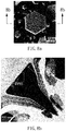
- FIG. 8 a is a top view of another sample of indium gallium nitride/gallium nitride quantum-well pyramid made by the embodiment according to the present invention.
- FIG. 8 b is a transmission electron microscopy image of the other sample shown in FIG. 8 a.
- FIG. 8 c is a high-angle annular dark-field image of the other sample shown in FIG. 8 a.
- FIG. 8 d is a magnified transmission electron microscopy image of a region DP 01 as shown in FIG. 8 b.
- FIG. 8 e is a magnified transmission electron microscopy image of a region HR 01 as shown in FIG. 8 d.
- FIG. 8 f is a magnified transmission electron microscopy image of a region HR 02 as shown in FIG. 8 d.
- FIG. 8 g is a magnified transmission electron microscopy image of a region HR 03 as shown in FIG. 8 d.
- FIG. 8 h is a magnified transmission electron microscopy image of a region HR 04 as shown in FIG. 8 d.
- electrophotonescence effect means recombination of an electron and an electron hole at a p-n junction of a light-emitting diode to emit lights while a current flows through the p-n junction of the light-emitting diode, which can be appreciated by one having ordinary skill in the art.
- wurtzite referred to herein means a crystal structure of a hexagonal crystal system, with the c-axis of the crystal structure is the [0001] direction of a 4-axis coordinate system, which can be appreciated by one having ordinary skill in the art.
- a method for manufacturing an indium gallium nitride/gallium nitride quantum-well pyramid includes a gallium nitride pyramid forming step S 1 , an indium gallium nitride layer forming step S 2 and a gallium nitride layer forming step S 3 .
- An indium gallium nitride/gallium nitride quantum-well pyramid is fabricated through the above steps.
- a substrate 1 for the indium gallium nitride/gallium nitride quantum-well pyramid to grow on can be cleaned to remove impurities on a surface of the substrate 1 , so as to enhance the quality of epitaxial product.
- the surface of the substrate 1 can be washed sequentially in acetone, isopropanol, deionized water, phosphoric acid solution and deionized water.
- the substrate 1 is heated (e.g. heated to 750° C. for 10 minutes) after the liquid on the surface of the substrate 1 is removed by nitrogen gas to assure that the surface of the substrate 1 is clean.
- the substrate 1 can be a LiAlO 2 substrate, a LiGaO 2 substrate or a ZnO substrate in order to enhance the lattice matching between the substrate and other materials (e.g. gallium nitride used in the following step) and to increase the success rate of the manufacturing process.
- materials e.g. gallium nitride used in the following step
- the gallium nitride pyramid forming step S 1 includes a first pyramid forming step S 11 and a second pyramid forming step S 12 , to fabricate a gallium nitride pyramid 2 by the two steps. Therefore, a size of the indium gallium nitride/gallium nitride quantum-well pyramid can be controlled.
- the first pyramid forming step S 11 is taken under 600-650° C. to form a semi-finished gallium nitride pyramid on the substrate 1 by performing a first epitaxial reaction on the substrate 1 , where a flux ratio of nitrogen to gallium of the first epitaxial reaction is 25:1-35:1.
- the first pyramid forming step S 11 can be taken under 630° C., with the flux ratio of nitrogen to gallium of the first epitaxial reaction being 29:1 and the first epitaxial reaction performed for 35 minutes.
- the semi-finished gallium nitride pyramid with good crystal structure can be obtained.
- the second pyramid forming step S 12 is taken under 600-650° C. to form the gallium nitride pyramid 2 from the semi-finished gallium nitride pyramid by performing a second epitaxial reaction on the substrate 1 , where a flux ratio of nitrogen to gallium of the second epitaxial reaction is 130:1-150:1.
- the second pyramid forming step S 12 can be taken under 630° C., with the flux ratio of nitrogen to gallium of the second epitaxial reaction being 138.8:1 and the second epitaxial reaction performed for 70 minutes.
- the gallium nitride pyramid 2 with good crystal structure can be obtained.
- the gallium nitride pyramid 2 includes an end face 2 a away from the substrate 1 .
- the end face 2 a with a large area is for following epitaxial reactions to be performed on.
- a gallium wetting layer 3 can be formed on the substrate 1 , and then the first epitaxial reaction is performed on the gallium wetting layer 3 . Due to the similarity of the material property between the gallium wetting layer 3 and gallium nitride for the gallium nitride pyramid 2 , the connection between the substrate 1 and the gallium nitride pyramid 2 is enhanced by applying the gallium wetting layer 3 and the success rate of epitaxy of the gallium nitride pyramid 2 is increased.
- the gallium wetting layer 3 can be formed by following steps: providing a vapor containing gallium under 630° C., and depositing gallium elements of the vapor containing gallium on the substrate 1 for 5 minutes to form the gallium wetting layer 3 on the surface of the substrate 1 .
- the indium gallium nitride forming step S 2 is aimed to form an indium gallium nitride layer 4 .
- An epitaxial reaction can be performed for 1.5 minutes under 780° C. with a flux ratio of indium to gallium to nitrogen be 1.55:1:165.09 (for example, the pressure of indium, gallium and nitrogen can be controlled at 8.5 ⁇ 10 ⁇ 8 , 5.5 ⁇ 10 ⁇ 8 and 9.08 ⁇ 10 ⁇ 6 Torr, respectively) to form a first indium gallium nitride layer 41 .
- an indium wetting layer 5 can be formed on the end face 2 a , and then the first indium gallium nitride layer 41 is grown on the indium wetting layer 5 . Due to the similarity of the material property between indium wetting layer 5 and indium gallium nitride for the first indium gallium nitride layer 41 , the connection between the gallium nitride pyramid 2 and the first indium gallium nitride layer 41 is enhanced by applying the indium wetting layer 5 and the success rate of epitaxy of the first indium gallium nitride layer 41 is increased.
- the indium wetting layer 5 can be formed by following steps: providing a vapor containing indium under 780° C., and depositing indium elements of the vapor containing indium on the end face 2 a for 1 minute to form the indium wetting layer 5 on the end face 2 a.
- the gallium nitride layer forming step S 3 is aimed to form a gallium nitride layer 6 on the indium gallium nitride 4 .
- the gallium nitride layer 6 can protect the indium gallium nitride layer 4 and the diffusion of ions into the indium gallium nitride layer 4 is avoided, so the service life of the indium gallium nitride layer 4 is increased.
- a gallium nitride epitaxial reaction can be preferably performed with a flux ratio of nitrogen to gallium being 165.09:1 (for example, the pressure of nitrogen and gallium can be controlled at 9.08 ⁇ 10 ⁇ 6 and 5.5 ⁇ 10 ⁇ 8 Torr, respectively).
- the gallium nitride epitaxial reaction can be performed for 30 seconds under 780° C. to fabricate a gallium nitride cap layer on the first indium gallium nitride layer 41 .
- gallium nitride epitaxial reaction can be preferably performed with a flux ratio of nitrogen to gallium being 70.39:1 (for example, the pressure of nitrogen and gallium can be controlled at 9.08 ⁇ 10 ⁇ 6 and 1.29 ⁇ 10 ⁇ 7 Torr, respectively).
- the other gallium nitride epitaxial reaction can be performed for 10 minutes under 780° C. to fabricate a gallium nitride barrier layer on the gallium nitride cap layer.
- the gallium nitride cap layer and the gallium nitride barrier layer jointly form a first gallium nitride layer 61 .
- the indium gallium nitride/gallium nitride quantum-well pyramid can be obtained, where the indium gallium nitride/gallium nitride quantum-well pyramid includes the gallium nitride pyramid 2 , the indium gallium nitride layer 4 and the gallium nitride layer 6 .
- the indium gallium nitride layer 4 can emit lights because of the electroluminescence effect.
- the color of lights emitted from the indium gallium nitride layer 4 is determined by the element ratio of the indium gallium nitride layer 4 .
- the indium gallium nitride layer 4 can emit lights with different colors if the element ratio of indium to gallium of the indium gallium nitride layer 4 is changed by adjusting the flux ratio of indium to gallium to nitrogen of the epitaxial reaction in the indium gallium nitride layer forming step S 2 .
- indium gallium nitride layers 4 and a plurality of gallium nitride layers 6 are able to fabricate a plurality of indium gallium nitride layers 4 and a plurality of gallium nitride layers 6 on the end face 2 a of the gallium nitride pyramid 2 by repeating the indium gallium nitride layer forming step S 2 and the gallium nitride layer forming step S 3 .
- the luminous efficiency of the indium gallium nitride/gallium nitride quantum-well pyramid is increased.
- the indium gallium nitride layer forming step S 2 and the gallium nitride layer forming step S 3 can be repeated twice after finishing the first time of the indium gallium nitride layer forming step S 2 and the gallium nitride layer forming step S 3 .
- a second and a third indium gallium nitride layers 42 , 43 and a second and a third gallium nitride layers 62 , 63 are formed, where the second indium gallium nitride 42 layer is on the first gallium nitride layer 61 , the second gallium nitride layer 62 is on the second indium gallium nitride layer 42 , the third indium gallium nitride layer 43 is on the second gallium nitride layer 62 , and the third gallium nitride layer 63 is on the third indium gallium nitride layer 43 , in order to form the layered structure shown in FIG. 3 .
- the element ratio of indium to gallium among the first, the second and the third indium gallium nitride layers 41 , 42 , 43 can be different in order for the first, the second and the third indium gallium nitride layers 41 , 42 , 43 to emit lights with different colors.
- a red-light indium gallium nitride layer, a green-light indium gallium nitride layer and a blue-light indium gallium nitride layer can be form as the three indium gallium nitride layers 4 . Therefore, the three indium gallium nitride layers 4 can emit lights of three primary colors, i.e. the three indium gallium nitride layers 4 can emit red light, green light and blue light. Lights of other colors can be emitted from the indium gallium nitride/gallium nitride quantum-well pyramid by modifying the intensity of the lights of three primary colors.
- a single indium gallium nitride/gallium nitride quantum-well pyramid can be utilized as a pixel of a display device, and the convenience of utilization of the indium gallium nitride/gallium nitride quantum-well pyramid is enhanced.
- FIG. 4 a is an SEM image of a plurality of indium gallium nitride/gallium nitride quantum-well pyramid samples on a substrate.
- a sample P and two regions bg 1 , bg 2 circled with broken lines are taken as the specimen and the background levels for following experiments respectively.
- the sample P, the region bg 1 and the region bg 2 are the indium gallium nitride/gallium nitride quantum-well pyramid, a three-dimensional c-plane of a gallium nitride wurtzite structure and a two-dimensional M-plane of the gallium nitride wurtzite structure respectively.
- FIGS. 4 b -4 e are magnified images of the sample P, where FIGS. 4 b and 4 d are top views of the sample P and FIGS. 4 c and 4 e are side views of the sample P.
- FIGS. 4 b -4 e show that the diameter of a top surface of the sample P, which does not connect with the substrate 1 , is about 2.9 ⁇ m, and that the sample P is in a form of a hexagonal pyramid.
- FIG. 5 is a PL spectrum of the sample P and the two regions bg 1 , bg 2 .
- FIG. 5 shows that three peaks are observed from the sample P at photon energy of (2.210 ⁇ 0.001), (2.935 ⁇ 0.001) and (3.359 ⁇ 0.001) eV, two peaks are observed from the region bg 1 at photon energy of (2.206 ⁇ 0.001) and (3.373 ⁇ 0.001) eV, and only one peak is observed from region bg 2 at photon energy of (3.412 ⁇ 0.002) eV.
- Peaks can be observed from the sample P, the region bg 1 and the region bg 2 when photon energy is 3.359-3.412 eV.
- the peaks observed at photon energy of 3.359-3.412 eV are attributed to the bandgap transition of the three-dimensional c-plane or the two-dimensional M-plane of the gallium nitride wurtzite structure.
- the value of the peaks observed from the sample P and the region bg 1 at photon energy of 3.359-3.412 eV is less than that from the region bg 2 due to the quantum size effect. Rest of peaks from the sample P and the region bg 1 will be analyzed by cathodoluminescence (CL) spectroscopy.
- CL cathodoluminescence
- FIG. 6 is a CL spectrum of the sample P and shows that three peaks are observed from the sample P at photon energy of (2.250 ⁇ 0.002), (2.893 ⁇ 0.003) and (3.371 ⁇ 0.002) eV.
- FIGS. 7 a -7 d are CL images of the sample P under room temperature.
- FIG. 7 a is a secondary electron image (SEI) of the sample P.
- FIG. 7 b is the CL image of the sample P at photon energy of 3.371 eV (photon wavelength ⁇ 336 nm). From FIG. 7 b , the peak at photon energy of 3.371 eV is attributed to bandgap transition of gallium nitride crystal with wurtzite structure, and, more particularly, is attributed to bandgap transition of gallium nitride crystals around the sample P.
- FIG. 7 c is the CL image of the sample P at photon energy of 2.893 eV (photon wavelength ⁇ 426 nm).
- FIG. 7 d is the CL image of the sample P at photon energy of 2.250 eV (photon wavelength ⁇ 555 nm). From FIG. 7 d , the peak at photon energy of 2.250 eV is attributed to bandgap transition or structural defect levels of both the sample P and the gallium nitride crystals around the sample P. From these results, the peak at photon energy of 2.893 eV can be observed only from the sample P with three-dimensional c-plane structure.
- FIG. 7 e is a secondary electron image (SEI) of the sample P under 10 K.
- FIG. 7 f is a CL image of the sample P at photon energy of 2.893 eV under 10 K.
- FIGS. 7 e -7 f show that the luminous intensity of the sample P is enhanced due to the quantum confinement effect.
- FIG. 8 a is an SEM image of another sample P′, where the other sample P′ is another indium gallium nitride/gallium nitride quantum-well pyramid.
- FIGS. 8 b -8 h are TEM images of the other sample P′ shown in FIG. 8 a
- FIGS. 8 b -8 h are taken of a longitudinal section of the other sample P′ divided along the 8 b - 8 b line in FIG. 8 a .
- FIGS. 8 b -8 h are observed along a [1 1 00] direction.
- FIG. 8 b shows that, the gallium nitride pyramid of the other sample P′ has lateral faces.
- the angle Al between each of the lateral faces and the c-axis of the 4-axis coordinate system is about 28°.
- the gallium nitride pyramid is grown into a form of an awl because of the lateral overgrowth of the epitaxial reactions. Specifically, the nitrogen atoms are caught by the edged gallium atoms during the epitaxial reactions, and thus make the gallium nitride pyramid into the form of the awl.
- FIG. 8 c is the high-angle annular dark-field (HAADF) image of the other sample P′.
- HAADF high-angle annular dark-field
- FIG. 8 d is a magnified image of region DP 01 in FIG. 8 b . It is measured that a distance D 1 between two of the three indium gallium nitride layers is 57.6 nm in FIG. 8 d .
- FIGS. 8 e -8 h are magnified images of region HR 01 -HR 04 respectively. Periodically aligned wurtzite structure of the gallium nitride pyramid is observed in FIG. 8 e .
- FIGS. 8 f -8 h it is observed that one of the three indium gallium nitride layers is formed between the gallium nitride pyramid and one of the three gallium nitride layers, or between two of the three gallium nitride layers.
- the gallium nitride pyramid is grown along a specific direction by applying different flux ratios of nitrogen to gallium in the first epitaxial reaction and the second epitaxial reaction.
- it is able to obtain a single indium gallium nitride/gallium nitride quantum-well pyramid die without a cutting step.
- the complexity of the manufacturing process is reduced and the convenience of controlling the size of a die is increased.
Landscapes
- Led Devices (AREA)
- Chemical & Material Sciences (AREA)
- Crystallography & Structural Chemistry (AREA)
Abstract
Description
Claims (14)
Applications Claiming Priority (3)
| Application Number | Priority Date | Filing Date | Title |
|---|---|---|---|
| TW107146512A | 2018-12-21 | ||
| TW107146512A TWI682053B (en) | 2018-12-21 | 2018-12-21 | Method for manufacturing indium gallium nitride/gallium nitride quantum-well reversed pyramid |
| TW107146512 | 2018-12-21 |
Publications (2)
| Publication Number | Publication Date |
|---|---|
| US20200203555A1 US20200203555A1 (en) | 2020-06-25 |
| US10811559B2 true US10811559B2 (en) | 2020-10-20 |
Family
ID=69942872
Family Applications (1)
| Application Number | Title | Priority Date | Filing Date |
|---|---|---|---|
| US16/232,285 Expired - Fee Related US10811559B2 (en) | 2018-12-21 | 2018-12-26 | Method for manufacturing indium gallium nitride/gallium nitride quantum-well pyramid |
Country Status (2)
| Country | Link |
|---|---|
| US (1) | US10811559B2 (en) |
| TW (1) | TWI682053B (en) |
Families Citing this family (2)
| Publication number | Priority date | Publication date | Assignee | Title |
|---|---|---|---|---|
| JP7081428B2 (en) | 2018-09-28 | 2022-06-07 | トヨタ自動車株式会社 | Precipitation index estimator |
| TWI857763B (en) * | 2023-08-25 | 2024-10-01 | 國立中山大學 | Method of forming indium gallium nitride quantum well structures |
Citations (4)
| Publication number | Priority date | Publication date | Assignee | Title |
|---|---|---|---|---|
| US20140110664A1 (en) * | 2012-10-19 | 2014-04-24 | National Sun Yat-Sen University | Iii-nitride quantum well structure, a method for producing the same, and a light-emitting unit using the same |
| CN104205294A (en) | 2012-02-14 | 2014-12-10 | 昆南诺股份有限公司 | Electronic devices based on gallium nitride nanowires |
| TWI500072B (en) | 2004-08-31 | 2015-09-11 | 學校法人上智學院 | Light-emitting element manufacturing method |
| US20170183776A1 (en) * | 2014-02-11 | 2017-06-29 | Kenneth Scott Alexander Butcher | Electrostatic control of metal wetting layers during deposition |
-
2018
- 2018-12-21 TW TW107146512A patent/TWI682053B/en not_active IP Right Cessation
- 2018-12-26 US US16/232,285 patent/US10811559B2/en not_active Expired - Fee Related
Patent Citations (8)
| Publication number | Priority date | Publication date | Assignee | Title |
|---|---|---|---|---|
| TWI500072B (en) | 2004-08-31 | 2015-09-11 | 學校法人上智學院 | Light-emitting element manufacturing method |
| US9362717B2 (en) | 2004-08-31 | 2016-06-07 | Sophia School Corporation | Columnar crystal containing light emitting element and method of manufacturing the same |
| US20160254138A1 (en) | 2004-08-31 | 2016-09-01 | Sophia School Corporation | Columnar crystal containing light emitting element and method of manufacturing the same |
| CN104205294A (en) | 2012-02-14 | 2014-12-10 | 昆南诺股份有限公司 | Electronic devices based on gallium nitride nanowires |
| US9653286B2 (en) | 2012-02-14 | 2017-05-16 | Hexagem Ab | Gallium nitride nanowire based electronics |
| US10236178B2 (en) | 2012-02-14 | 2019-03-19 | Hexagem Ab | Gallium nitride nanowire based electronics |
| US20140110664A1 (en) * | 2012-10-19 | 2014-04-24 | National Sun Yat-Sen University | Iii-nitride quantum well structure, a method for producing the same, and a light-emitting unit using the same |
| US20170183776A1 (en) * | 2014-02-11 | 2017-06-29 | Kenneth Scott Alexander Butcher | Electrostatic control of metal wetting layers during deposition |
Also Published As
| Publication number | Publication date |
|---|---|
| US20200203555A1 (en) | 2020-06-25 |
| TWI682053B (en) | 2020-01-11 |
| TW202024385A (en) | 2020-07-01 |
Similar Documents
| Publication | Publication Date | Title |
|---|---|---|
| US8735867B2 (en) | Group III nitride nanorod light emitting device | |
| TWI419368B (en) | Group III nitride compound semiconductor light-emitting element and method of manufacturing same | |
| JP2012033893A (en) | Group iii nitride light-emitting diode | |
| US20250176316A1 (en) | Semiconductor template and fabrication method | |
| US11322649B2 (en) | Three color light sources integrated on a single wafer | |
| US20110175126A1 (en) | Light-emitting diode structure | |
| Yang et al. | InGaN/GaN multiple quantum wells on selectively grown GaN microfacets and the applications for phosphor-free white light-emitting diodes | |
| US10811559B2 (en) | Method for manufacturing indium gallium nitride/gallium nitride quantum-well pyramid | |
| US8916458B2 (en) | III-nitride quantum well structure, a method for producing the same, and a light-emitting unit using the same | |
| Gustafsson et al. | From InGaN pyramids to micro-LEDs characterized by cathodoluminescence | |
| Funato et al. | A review of three-dimensional structure-controlled InGaN quantum wells for efficient visible polychromatic light emitters | |
| TWI540752B (en) | Luminescent body with three-group nitride quantum well structure | |
| US20230073455A1 (en) | Group-iii-nitride structures and manufacturing methods thereof | |
| TWI889830B (en) | Optoelectronic device and manufacturing method thereof | |
| Cho et al. | High quality GaN tetrapodal structures hetero-integrated on 3D Si surfaces | |
| Kapoor | Core-shell InGaN/GaN wires for flexible LEDs | |
| Li et al. | Confocal microscopy study on spatial variation of photoluminescence in blue-emitting InGaN/GaN MQWs with different growth parameters | |
| US9728404B2 (en) | Method of growing nitride semiconductor layer, nitride semiconductor device, and method of fabricating the same | |
| EP4521475A1 (en) | Semiconductor structure, optoelectronic device and fabrication method | |
| O’Neill et al. | Defect observations in GaN MQW structures | |
| US20250072164A1 (en) | Method of forming indium gallium nitride quantum well structure | |
| GB2636348A (en) | Light emitting diode | |
| Rais et al. | Fabrication of InxGa1-xN/GaN Multi-Quantum Well Structure for Green Light Emitting Diode on Patterned Sapphire Substrate by Metal Organic Chemical Vapour Deposition | |
| Li et al. | Multifacet microrod light-emitting diode with full visible spectrum emission | |
| Albert et al. | Selective area growth of III-nitride nanorods on polar, semi-polar, and non-polar orientations: device applications |
Legal Events
| Date | Code | Title | Description |
|---|---|---|---|
| AS | Assignment |
Owner name: NATIONAL SUN YAT-SEN UNIVERSITY, TAIWAN Free format text: ASSIGNMENT OF ASSIGNORS INTEREST;ASSIGNORS:LO, I-KAI;TSAI, CHENG-DA;WANG, YING-CHIEH;AND OTHERS;REEL/FRAME:047852/0168 Effective date: 20181130 |
|
| FEPP | Fee payment procedure |
Free format text: ENTITY STATUS SET TO UNDISCOUNTED (ORIGINAL EVENT CODE: BIG.); ENTITY STATUS OF PATENT OWNER: SMALL ENTITY |
|
| FEPP | Fee payment procedure |
Free format text: ENTITY STATUS SET TO SMALL (ORIGINAL EVENT CODE: SMAL); ENTITY STATUS OF PATENT OWNER: SMALL ENTITY |
|
| STPP | Information on status: patent application and granting procedure in general |
Free format text: FINAL REJECTION MAILED |
|
| STPP | Information on status: patent application and granting procedure in general |
Free format text: PUBLICATIONS -- ISSUE FEE PAYMENT RECEIVED |
|
| STCF | Information on status: patent grant |
Free format text: PATENTED CASE |
|
| FEPP | Fee payment procedure |
Free format text: MAINTENANCE FEE REMINDER MAILED (ORIGINAL EVENT CODE: REM.); ENTITY STATUS OF PATENT OWNER: SMALL ENTITY |
|
| LAPS | Lapse for failure to pay maintenance fees |
Free format text: PATENT EXPIRED FOR FAILURE TO PAY MAINTENANCE FEES (ORIGINAL EVENT CODE: EXP.); ENTITY STATUS OF PATENT OWNER: SMALL ENTITY |
|
| STCH | Information on status: patent discontinuation |
Free format text: PATENT EXPIRED DUE TO NONPAYMENT OF MAINTENANCE FEES UNDER 37 CFR 1.362 |
|
| FP | Lapsed due to failure to pay maintenance fee |
Effective date: 20241020 |