US10790286B2 - Apparatuses including 3D memory arrays, methods of forming the apparatuses, and related electronic systems - Google Patents
Apparatuses including 3D memory arrays, methods of forming the apparatuses, and related electronic systems Download PDFInfo
- Publication number
- US10790286B2 US10790286B2 US16/212,418 US201816212418A US10790286B2 US 10790286 B2 US10790286 B2 US 10790286B2 US 201816212418 A US201816212418 A US 201816212418A US 10790286 B2 US10790286 B2 US 10790286B2
- Authority
- US
- United States
- Prior art keywords
- odd
- digit
- lines
- group
- digit lines
- Prior art date
- Legal status (The legal status is an assumption and is not a legal conclusion. Google has not performed a legal analysis and makes no representation as to the accuracy of the status listed.)
- Active, expires
Links
Images


Classifications
-
- H01L27/108—
-
- G—PHYSICS
- G11—INFORMATION STORAGE
- G11C—STATIC STORES
- G11C11/00—Digital stores characterised by the use of particular electric or magnetic storage elements; Storage elements therefor
- G11C11/21—Digital stores characterised by the use of particular electric or magnetic storage elements; Storage elements therefor using electric elements
- G11C11/34—Digital stores characterised by the use of particular electric or magnetic storage elements; Storage elements therefor using electric elements using semiconductor devices
- G11C11/40—Digital stores characterised by the use of particular electric or magnetic storage elements; Storage elements therefor using electric elements using semiconductor devices using transistors
- G11C11/401—Digital stores characterised by the use of particular electric or magnetic storage elements; Storage elements therefor using electric elements using semiconductor devices using transistors forming cells needing refreshing or charge regeneration, i.e. dynamic cells
- G11C11/403—Digital stores characterised by the use of particular electric or magnetic storage elements; Storage elements therefor using electric elements using semiconductor devices using transistors forming cells needing refreshing or charge regeneration, i.e. dynamic cells with charge regeneration common to a multiplicity of memory cells, i.e. external refresh
- G11C11/405—Digital stores characterised by the use of particular electric or magnetic storage elements; Storage elements therefor using electric elements using semiconductor devices using transistors forming cells needing refreshing or charge regeneration, i.e. dynamic cells with charge regeneration common to a multiplicity of memory cells, i.e. external refresh with three charge-transfer gates, e.g. MOS transistors, per cell
-
- H—ELECTRICITY
- H10—SEMICONDUCTOR DEVICES; ELECTRIC SOLID-STATE DEVICES NOT OTHERWISE PROVIDED FOR
- H10B—ELECTRONIC MEMORY DEVICES
- H10B12/00—Dynamic random access memory [DRAM] devices
-
- G—PHYSICS
- G11—INFORMATION STORAGE
- G11C—STATIC STORES
- G11C11/00—Digital stores characterised by the use of particular electric or magnetic storage elements; Storage elements therefor
- G11C11/21—Digital stores characterised by the use of particular electric or magnetic storage elements; Storage elements therefor using electric elements
- G11C11/34—Digital stores characterised by the use of particular electric or magnetic storage elements; Storage elements therefor using electric elements using semiconductor devices
- G11C11/40—Digital stores characterised by the use of particular electric or magnetic storage elements; Storage elements therefor using electric elements using semiconductor devices using transistors
- G11C11/401—Digital stores characterised by the use of particular electric or magnetic storage elements; Storage elements therefor using electric elements using semiconductor devices using transistors forming cells needing refreshing or charge regeneration, i.e. dynamic cells
- G11C11/4063—Auxiliary circuits, e.g. for addressing, decoding, driving, writing, sensing or timing
- G11C11/407—Auxiliary circuits, e.g. for addressing, decoding, driving, writing, sensing or timing for memory cells of the field-effect type
- G11C11/408—Address circuits
- G11C11/4085—Word line control circuits, e.g. word line drivers, - boosters, - pull-up, - pull-down, - precharge
-
- G—PHYSICS
- G11—INFORMATION STORAGE
- G11C—STATIC STORES
- G11C11/00—Digital stores characterised by the use of particular electric or magnetic storage elements; Storage elements therefor
- G11C11/21—Digital stores characterised by the use of particular electric or magnetic storage elements; Storage elements therefor using electric elements
- G11C11/34—Digital stores characterised by the use of particular electric or magnetic storage elements; Storage elements therefor using electric elements using semiconductor devices
- G11C11/40—Digital stores characterised by the use of particular electric or magnetic storage elements; Storage elements therefor using electric elements using semiconductor devices using transistors
- G11C11/401—Digital stores characterised by the use of particular electric or magnetic storage elements; Storage elements therefor using electric elements using semiconductor devices using transistors forming cells needing refreshing or charge regeneration, i.e. dynamic cells
- G11C11/4063—Auxiliary circuits, e.g. for addressing, decoding, driving, writing, sensing or timing
- G11C11/407—Auxiliary circuits, e.g. for addressing, decoding, driving, writing, sensing or timing for memory cells of the field-effect type
- G11C11/409—Read-write [R-W] circuits
- G11C11/4091—Sense or sense/refresh amplifiers, or associated sense circuitry, e.g. for coupled bit-line precharging, equalising or isolating
-
- H01L23/528—
-
- H01L27/10844—
-
- H01L27/10897—
-
- H01L28/60—
-
- H—ELECTRICITY
- H10—SEMICONDUCTOR DEVICES; ELECTRIC SOLID-STATE DEVICES NOT OTHERWISE PROVIDED FOR
- H10B—ELECTRONIC MEMORY DEVICES
- H10B12/00—Dynamic random access memory [DRAM] devices
- H10B12/01—Manufacture or treatment
-
- H—ELECTRICITY
- H10—SEMICONDUCTOR DEVICES; ELECTRIC SOLID-STATE DEVICES NOT OTHERWISE PROVIDED FOR
- H10B—ELECTRONIC MEMORY DEVICES
- H10B12/00—Dynamic random access memory [DRAM] devices
- H10B12/50—Peripheral circuit region structures
-
- H—ELECTRICITY
- H10—SEMICONDUCTOR DEVICES; ELECTRIC SOLID-STATE DEVICES NOT OTHERWISE PROVIDED FOR
- H10D—INORGANIC ELECTRIC SEMICONDUCTOR DEVICES
- H10D1/00—Resistors, capacitors or inductors
- H10D1/60—Capacitors
- H10D1/68—Capacitors having no potential barriers
- H10D1/692—Electrodes
-
- H—ELECTRICITY
- H10—SEMICONDUCTOR DEVICES; ELECTRIC SOLID-STATE DEVICES NOT OTHERWISE PROVIDED FOR
- H10W—GENERIC PACKAGES, INTERCONNECTIONS, CONNECTORS OR OTHER CONSTRUCTIONAL DETAILS OF DEVICES COVERED BY CLASS H10
- H10W20/00—Interconnections in chips, wafers or substrates
- H10W20/40—Interconnections external to wafers or substrates, e.g. back-end-of-line [BEOL] metallisations or vias connecting to gate electrodes
- H10W20/41—Interconnections external to wafers or substrates, e.g. back-end-of-line [BEOL] metallisations or vias connecting to gate electrodes characterised by their conductive parts
- H10W20/43—Layouts of interconnections
-
- G—PHYSICS
- G11—INFORMATION STORAGE
- G11C—STATIC STORES
- G11C11/00—Digital stores characterised by the use of particular electric or magnetic storage elements; Storage elements therefor
- G11C11/21—Digital stores characterised by the use of particular electric or magnetic storage elements; Storage elements therefor using electric elements
- G11C11/34—Digital stores characterised by the use of particular electric or magnetic storage elements; Storage elements therefor using electric elements using semiconductor devices
- G11C11/40—Digital stores characterised by the use of particular electric or magnetic storage elements; Storage elements therefor using electric elements using semiconductor devices using transistors
- G11C11/401—Digital stores characterised by the use of particular electric or magnetic storage elements; Storage elements therefor using electric elements using semiconductor devices using transistors forming cells needing refreshing or charge regeneration, i.e. dynamic cells
- G11C11/4063—Auxiliary circuits, e.g. for addressing, decoding, driving, writing, sensing or timing
- G11C11/407—Auxiliary circuits, e.g. for addressing, decoding, driving, writing, sensing or timing for memory cells of the field-effect type
- G11C11/409—Read-write [R-W] circuits
- G11C11/4097—Bit-line organisation, e.g. bit-line layout, folded bit lines
Definitions
- Embodiments of the disclosure relate to the field of semiconductor device design and fabrication. More specifically, embodiments of the present disclosure relate to apparatuses including 3D memory arrays, to methods of forming the apparatuses, and to related electronic systems.
- semiconductor device designers often desire to increase the level of integration or density of features within a semiconductor device by reducing the dimensions of the individual features and by reducing the separation distance between neighboring features.
- semiconductor device designers often desire to design architectures that are not only compact, but offer performance advantages, as well as simplified designs.
- Memory devices are generally provided as internal integrated circuits in computers or other electronic devices. There are many types of memory including, but not limited to, random-access memory (RAM), read only memory (ROM), dynamic random access memory (DRAM), synchronous dynamic random access memory (SDRAM), flash memory, and resistance variable remory.
- RAM random-access memory
- ROM read only memory
- DRAM dynamic random access memory
- SDRAM synchronous dynamic random access memory
- flash memory and resistance variable remory.
- Non-limiting examples of resi stance variable memory include resistive random access memory (RRAM), conductive bridge random access memory (conductive bridge RAM), magnetic random access memory (MRAM), phase change material (PCM) memory, phase change random access memory (PCRAM), spin-torque-transfer random access memory (STTRAM), oxygen vacancy-based memory, and programmable conductor memory.
- RRAM resistive random access memory
- MRAM magnetic random access memory
- PCM phase change material
- PCRAM phase change random access memory
- STTRAM spin-torque-trans
- a typical memory cell of a memory device includes one access device, such as a transistor, and one memory storage structure, such as a capacitor.
- Modern applications for semiconductor devices can employ significant quantities of memory cells, arranged in memory arrays exhibiting rows and columns of the memory cells.
- the memory cells may be electrically accessed through digit lines (e.g., bit lines, data lines) and word lines (e.g., access lines) arranged along the rows and columns of the memory cells of the memory arrays.
- Memory arrays can be two-dimensional (2D) so as to exhibit a single deck (e.g., a single tier, a single level) of the memory cells, or can be three-dimensional (3D) so as to exhibit multiple decks (e.g., multiple levels, multiple tiers) of the memory cells.
- Control logic devices within a base structure underlying a memory array of a memory device have been used to control operations (e.g., access operations, read operations, write operations) on the memory cells of the memory device.
- An assembly of the control logic devices may be provided in electrical communication with the memory cells of the memory array by way of routing and interconnect structures.
- electrically connecting the memory cells of the different decks of the 3D memory array to the assembly of control logic devices within the base control logic structure can create sizing and spacing complications associated with the increased quantities and dimensions of routing and interconnect structures required to facilitate the electrical connection.
- the quantities, dimensions, and arrangements of the different control logic devices employed within the base control logic structure can also undesirably impede reductions to the size of a memory device, increases to the storage density of the memory device, and/or reductions in fabrication costs.
- FIG. 1 is a simplified side elevation schematic view of an apparatus, in accordance with embodiments of the disclosure.
- FIG. 2 is simplified top-down schematic view of the apparatus shown in FIG. 1 , in accordance with embodiments of the disclosure.
- FIG. 3 is a simplified side elevation electrical schematic view of the apparatus shown in FIG. 1 , in accordance with embodiments of the disclosure.
- FIGS. 4 and 5 are simplified plan views showing digit line termination regions within the apparatus shown in FIG. 1 , in accordance with embodiments of the disclosure.
- FIG. 6 is a simplified perspective view showing word line termination regions within the apparatus shown in FIG. 1 , in accordance with embodiments of the disclosure.
- FIG. 7 is a simplified plan view of an orthogonal quilt layout of the base structure of the apparatus shown in FIG. 1 , in accordance with embodiments of the disclosure.
- FIG. 8 is a simplified plan view showing a portion of the orthogonal quilt layout shown in FIG. 7 in more detail.
- FIG. 9 is a simplified plan view of a woven quilt layout of the base structure of the apparatus shown in FIG. 1 , in accordance with additional embodiments of the disclosure.
- FIG. 10 is a simplified plan view of a non-quilted layout of the base structure of the apparatus shown in FIG. 1 , in accordance with further embodiments of the disclosure.
- FIGS. 11A through 11N are simplified cross-sectional views illustrating embodiments of a method of forming an apparatus structure, in accordance with embodiments of the disclosure.
- FIG. 12 is a block diagram of an illustrative electronic system according to embodiments of the disclosure.
- the terms “configured” and “configuration” refer to a size, shape, material composition, material distribution, orientation, and arrangement of one or more of at least one structure and at least one apparatus facilitating operation of one or more of the structure and the apparatus in a predetermined way.
- the terms “longitudinal,” “vertical,” “lateral,” and “horizontal” are in reference to a major plane of a substrate (e.g., base material, base structure, base construction, etc.) in or on which one or more structures and/or features are formed and are not necessarily defined by earth's gravitational field.
- a “lateral” or “horizontal” direction is a direction that is substantially parallel to the major plane of the substrate, while a “longitudinal” or “vertical” direction is a direction that is substantially perpendicular to the major plane of the substrate.
- the major plane of the substrate is defined by a surface of the substrate having a relatively large area compared to other surfaces of the substrate.
- vertical-neighboring or “longitudinally-neighboring” features (e.g., structures, devices) means and includes features located most vertically proximate (e.g., vertically closest) one another.
- horizontal-neighboring or “laterally-neighboring” features (e.g., structures, devices) means and includes features located most horizontally proximate (e.g., horizontally closest) one another.
- spatially relative terms such as “beneath,” “below,” “lower,” “bottom,” “above,” “upper,” “top,” “front,” “rear,” “left,” “right,” and the like, may be used for ease of description to describe one element's or feature's relationship to another element(s) or feature(s) as illustrated in the figures.
- the spatially relative terms are intended to encompass different orientations of the materials in addition to the orientation depicted in the figures. For example, if materials in the figures are inverted, elements described as “below” or “beneath” or “under” or “on bottom of” other elements or features would then be oriented “above” or “on top of” the other elements or features.
- the term “below” can encompass both an orientation of above and below, depending on the context in which the term is used, which will be evident to one of ordinary skill in the art.
- the materials may be otherwise oriented (e.g., rotated 90 degrees, inverted, flipped, etc.) and the spatially relative descriptors used herein interpreted accordingly.
- the term “substantially” in reference to a given parameter, property, or condition means and includes to a degree that one of ordinary skill in the art would understand that the given parameter, property, or condition is met with a degree of variance, such as within acceptable manufacturing tolerances.
- the parameter, property, or condition may be at least 90.0% met, at least 95.0% met, at least 99.0% met, at least 99.9% met, or even 100.0% met.
- FIG. 1 shows a simplified side elevation schematic view of an apparatus 100 (e.g., a semiconductor device; a memory device, such as a DRAM device), in accordance with embodiments of the disclosure.
- the apparatus 100 includes a memory structure 101 and a base structure 104 underlying the memory structure 101 .
- the memory structure 101 includes a plurality of 3D memory arrays 103 each including a plurality of memory decks 102 (e.g., memory levels, memory tiers) in a vertically stacked arrangement relative to one another.
- the memory decks 102 of each 3D memory array 103 are each in electrical communication with the base structure 104 .
- FIG. 1 shows a simplified side elevation schematic view of an apparatus 100 (e.g., a semiconductor device; a memory device, such as a DRAM device), in accordance with embodiments of the disclosure.
- the apparatus 100 includes a memory structure 101 and a base structure 104 underlying the memory structure 101 .
- the memory structure 101 includes a plurality of 3D memory
- FIG. 2 illustrates a simplified, partial top-down schematic view of the apparatus 100 shown in FIG. 1 .
- FIG. 2 shows components of the third memory deck 102 C of one of the 3D memory arrays 103 of the memory structure 101 of the apparatus 100 , as well as components of the base structure 104 thereunder electrically connected to the components of the third memory deck 102 C.
- the other memory decks 102 e.g., the first memory deck 102 A ( FIG. 1 ), the second memory deck 102 B ( FIG. 1 )
- the 3D memory array 103 may exhibit similar components and component arrangements to those of the third memory deck 102 C.
- the odd digit lines 110 may be connected to and route from (e.g., in the negative Y-direction) the odd digit line interconnect structures 126 at first peripheral end of the 3D memory array 103
- the even digit lines 112 may be connected to and route from (e.g., in the positive Y-direction) the even digit line interconnect structures 128 at a second peripheral end of the 3D memory array 103 opposing the first peripheral end of the 3D memory array 103 .
- the word lines 114 of the memory deck 102 include odd word lines 116 and even word lines 118 .
- the odd word lines 116 laterally alternate (e.g., in the Y-direction) with the even word lines 118 .
- Some rows of the memory cells 120 are operatively associated with the odd word lines 116
- additional rows of the memory cells 120 are operatively associated with the even word lines 118 .
- the word lines 114 e.g., the odd word lines 116 and the even word lines 118
- the odd word lines 116 may be connected to and route from (e.g., in the positive X-direction) the odd word line interconnect structures 134 at third peripheral end of the 3D memory array 103
- the even word lines 118 may be connected to and route from (e.g., in the negative X-direction) the even word line interconnect structures 136 at a fourth peripheral end of the 3D memory array 103 opposing the third peripheral end of the 3D memory array 103 .
- each of the memory cells 120 may comprise two (2) transistors, and one (1) capacitor vertically between and electrically coupled to the two (2) transistors.
- the vertical arrangement of the two (2) transistors of each of the memory cells 120 may permit the digit lines 108 operatively associated with the memory cells 120 to be relatively shorter than the digit lines of conventional configurations, reducing digit line resistance and making it relatively easier to drive current through the digit lines 108 .
- each of the memory cells 120 may be operatively associated with two (2) of the digit lines 108 .
- the first odd digit line 110 may be connected to a first odd digit line interconnect structure 126 electrically connected to an odd sense amplifier 122 ; and the second odd digit line 110 may be connected to a second odd digit line interconnect structure 126 electrically connected to the odd sense amplifier 122 .
- additional columns of the memory cells 120 operatively associated with the even digit lines 112 may each individually exhibit a first even digit line 112 thereunder (or thereover) and a second even digit line 112 thereover (or thereunder).
- the first even digit line 112 may underlie and be connected to first (e.g., lower) transistors of the memory cells 120 of the additional column, and the second even digit line 112 may overlie and be connected to second (e.g., upper) transistors of the memory cells 120 of the additional column.
- the first even digit line 112 may be connected to a first even digit line interconnect structure 128 electrically connected to an even sense amplifier 124 ; and the second even digit line 112 may be connected to a second even digit line interconnect structure 128 electrically connected to the even sense amplifier 124 .
- the third memory deck 102 C (as well as the other memory decks 102 ( FIG. 1 ) of the 3D memory array 103 including the third memory deck 102 C, and the memory decks 102 ( FIG. 1 ) of each other 3D memory array 103 of the memory structure 101 ) includes a hexagonal pattern (e.g., a hexagonal arrangement, a hexagonal grid, a hexagonal array) of the memory cells 120 .
- the hexagonal pattern exhibits a repeating lateral arrangement of seven (7) memory cells 120 , wherein one (1) of the seven (7) memory cells 120 is substantially laterally centered between six (6) other of the seven (7) memory cells 120 .
- the hexagonal pattern exhibits different three (3) axes of symmetry 115 (e.g., a first axis of symmetry 115 A, a second axis of symmetry 115 B, and a third axis of symmetry 115 C) in the same lateral plane (e.g., the XY plane) about a center of the laterally-centered memory cell 120 of the seven (7) memory cells 120 .
- axes of symmetry 115 e.g., a first axis of symmetry 115 A, a second axis of symmetry 115 B, and a third axis of symmetry 115 C
- the same lateral plane e.g., the XY plane
- FIG. 1 are configured and positioned to facilitate the hexagonal pattern of the memory cells 120 of each of the memory decks 102 ( FIG. 1 ) of each of the 3D memory arrays 103 ( FIG. 1 ) of the memory structure 101 ( FIG. 1 ), as described in further detail below.
- FIG. 3 shows a simplified, partial side elevation electrical schematic view of the apparatus 100 shown in FIG. 1 .
- FIG. 3 depicts one of the 3D memory arrays 103 of the memory structure 101 , as well as interactions between components of the 3D memory array 103 and components of the base structure 104 . As shown in FIG.
- the memory cells 120 of each of the memory decks 102 each individually include a first transistor 120 A (e.g., a vertically lower transistor), a second transistor 120 B (e.g., a vertically upper transistor), and a capacitor 120 C (e.g., storage node structure) vertically between and electrically coupled to the first transistor 120 A and the second transistor 120 B.
- a first transistor 120 A e.g., a vertically lower transistor
- a second transistor 120 B e.g., a vertically upper transistor
- a capacitor 120 C e.g., storage node structure
- some of the memory cells 120 are connected to a pair of odd digit lines 110 and other of the memory cells 120 are connected to a pair of even digit lines 112 .
- first transistors 120 A of a portion of the memory cells 120 within the first memory deck 102 A may be connected to a first odd digit line 110 A and second transistors 120 B of the portion of the memory cells 120 may be connected to a second odd digit line 110 B overlying the first odd digit line 110 A; and first transistors 120 A of another portion of the memory cells 120 within the first memory deck 102 A may be connected to a first even digit line 112 A and second transistors 120 B of the another portion of the memory cells 120 may be connected to a second even digit line 112 B overlying the first even digit line 112 A.
- first transistors 120 A of a portion of the memory cells 120 within the second memory deck 102 B may be connected to the second odd digit line 110 B and second transistors 120 B of the portion of the memory cells 120 may be connected to a third odd digit line 110 C overlying the second odd digit line 110 B; and first transistors 120 A of another portion of the memory cells 120 within the second memory deck 102 B may be connected to the second even digit line 112 B and second transistors 120 B of the another portion of the memory cells 120 may be connected to a third even digit line 112 C overlying the second even digit line 112 B.
- first transistors 120 A of a portion of the memory cells 120 within the third memory deck 102 C may be connected to the third odd digit line 110 C and second transistors 120 B of the portion of the memory cells 120 may be connected to a fourth odd digit line 110 D overlying the third odd digit line 110 C; and first transistors 120 A of another portion of the memory cells 120 within the third memory deck 102 C may be connected to the third even digit line 112 C and second transistors 120 B of the another portion of the memory cells 120 may be connected to a fourth even digit line 112 D overlying the third even digit line 112 C.
- an odd sense amplifier 122 (e.g., one of the first odd sense amplifier 122 A, the second odd sense amplifier 122 B, and the third odd sense amplifier 122 C shown in FIG. 2 ) is electrically connected to a vertical stack of the odd digit lines 110 (e.g., the first odd digit line 110 A, the second odd digit line 110 B, the third odd digit line 110 C, and the fourth odd digit line 110 D); and an even sense amplifier 124 (e.g., one of the first even sense amplifier 124 A, the second even sense amplifier 124 B, and the third even sense amplifier 124 C shown in FIG.
- the odd sense amplifier 122 is electrically connected to a pair of odd base digit lines 138 , including a first odd base digit line 138 A (e.g., a “true” digit line) and a second odd base digit line 138 B (e.g., a “complementary” digit line, a digit bar line).
- a first odd base digit line 138 A e.g., a “true” digit line
- a second odd base digit line 138 B e.g., a “complementary” digit line, a digit bar line.
- the first odd base digit line 138 A and the second odd base digit line 138 B may connect to different regions (e.g., opposing ends) of the odd sense amplifier 122 than one another, and may be positioned laterally adjacent one another within the base structure 104 .
- the even sense amplifier 124 is electrically connected to a pair of even base digit lines 140 , including a first even base digit line 140 A (e.g., an additional “true” digit line) and a second even base digit line 140 B (e.g., an additional “complementary” digit line, an additional digit bar line).
- the first even base digit line 140 A and the second even base digit line 140 B may connect to different regions (e.g., opposing ends) of the even sense amplifier 124 than one another, and may be positioned laterally adjacent one another within the base structure 104 .
- the odd base digit lines 138 (e.g., the first odd base digit line 138 A, the second odd base digit line 138 B) connected to the odd sense amplifier 122 within the base structure 104 may be electrically connected to the odd digit lines 110 (e.g., the first odd digit line 110 A, the second odd digit line 110 B, the third odd digit line 110 C, and the fourth odd digit line 110 D) of the vertical stack of the odd digit lines 110 by way of the odd digit line interconnect structures 126 . As shown in FIG.
- the first odd digit line 110 A may be electrically connected to the first odd base digit line 138 A through a first odd digit line interconnect structure 126 A extending (e.g., vertically extending) between the first odd digit line 110 A and the first odd base digit line 138 A.
- the second odd digit line 110 B may be electrically connected to the second odd base digit line 138 B through a second odd digit line interconnect structure 126 B extending (e.g., vertically extending) between the second odd digit line 110 B and the second odd base digit line 138 B.
- the third odd digit line 110 C may be electrically connected to the first odd base digit line 138 A through a third odd digit line interconnect structure 126 C extending (e.g., vertically extending) between the third odd digit line 110 C and the first odd base digit line 138 A.
- the fourth odd digit line 110 D may be electrically connected to the second odd base digit line 138 B through a fourth odd digit line interconnect structure 126 D extending (e.g., vertically extending) between the fourth odd digit line 110 D and the second odd base digit line 138 B.
- the even base digit lines 140 (e.g., the first even base digit line 140 A, the second even base digit line 140 B) connected to the even sense amplifier 124 within the base structure 104 may be electrically connected to the even digit lines 112 (e.g., the first even digit line 112 A, the second even digit line 112 B, the third even digit line 112 C, and the fourth even digit line 112 D) of the vertical stack of the even digit lines 112 by way of the even digit line interconnect structures 128 . As shown in FIG.
- the first even digit line 112 A may be electrically connected to the second even base digit line 140 B through a first even digit line interconnect structure 128 A extending (e.g., vertically extending) between the first even digit line 112 A and the second even base digit line 140 B.
- the second even digit line 112 B may be electrically connected to the first even base digit line 140 A through a second even digit line interconnect structure 128 B extending (e.g., vertically extending) between the second even digit line 112 B and the first even base digit line 140 A.
- the third even digit line 112 C may be electrically connected to the second even base digit line 140 B through a third even digit line interconnect structure 128 C extending (e.g., vertically extending) between the third even digit line 112 C and the second even base digit line 140 B.
- the fourth even digit line 112 D may be electrically connected to the first even base digit line 140 A through a fourth even digit line interconnect structure 140 D extending (e.g., vertically extending) between the fourth even digit line 112 D and the first even base digit line 140 A.
- FIG. 3 depicts the vertical stack of the odd digit lines 110 (as well as the portion of the memory cells 120 , the odd sense amplifier 122 , the odd base digit lines 138 , and the odd digit line interconnect structures 126 operatively associated therewith) as being positioned laterally adjacent the vertical stack of the even digit lines 112 in the Y-direction (as well as the additional portion of the memory cells 120 , the even sense amplifier 124 , the even base digit lines 140 , and the even digit line interconnect structures 128 operatively associated therewith).
- the vertical stack of the even digit lines 112 (as well as the additional portion of the memory cells 120 , the even sense amplifier 124 , the even base digit lines 140 , and the even digit line interconnect structures 128 operatively associated therewith) would be positioned behind (e.g., into the page) the vertical stack of the odd digit lines 110 (as well as the portion of the memory cells 120 , the odd sense amplifier 122 , the odd base digit lines 138 , and the odd digit line interconnect structures 126 operatively associated therewith), such that the vertical stack of the even digit lines 112 is positioned laterally adjacent the vertical stack of the odd digit lines 110 in the X-direction in a manner consistent with the arrangement (e.g., layout, pattern) depicted in FIG. 2 .
- odd digit line interconnect structures 126 e.g., the first odd digit line interconnect structure 126 A, the second odd digit line interconnect structure 126 B, the third odd digit line interconnect structure 126 C, the fourth odd digit line interconnect structure 126 D
- odd digit line interconnect structures 126 associated with different odd digit lines 110 (e.g., the first odd digit line 110 A, the second odd digit line 110 B, the third odd digit line 110 C, the fourth odd digit line 110 D) of individual vertical stacks of the odd digit lines 110 may be at least partially laterally offset from (e.g., unaligned with) one another (e.g., in the Y-direction) to facilitate connection to ends of the different odd digit lines 110 .
- laterally-winding paths e.g., routes
- laterally-winding paths at the ends of the different odd digit lines 110 and/or laterally-winding conductive routing structures coupled to but vertically offset from the ends of the different odd digit lines 110 may also be employed to connect the different odd digit lines 110 to the odd digit line interconnect structures 126 .
- FIGS. 4 and 5 show the connections between different odd digit line interconnect structures 126 and the different odd digit lines 110 of one of the 3D memory arrays 103 of the memory structure 101 of the apparatus 100 .
- FIG. 4 illustrates a simplified plan view of digit line termination regions for first odd digit lines 110 A and second odd digit lines 110 B of different vertical stacks of odd digit lines 110 ( FIG. 3 ).
- the dashed rectangle 127 surrounds a grouping of four (4) different odd digit line interconnect structures 126 (e.g., including a first odd digit line interconnect structure 126 A, a second odd digit line interconnect structure 126 B, a third odd digit line interconnect structure 126 C, and a fourth odd digit line interconnect structure 126 D) that may be operatively associate with a single (e.g., only one) vertical stack of odd digit lines 110 ( FIG. 3 ) and a single odd sense amplifier 122 ( FIG.
- the grouping pattern is repeated throughout in the X-direction, with each grouping individually corresponding to different odd digit line interconnect structures 126 ( FIG. 3 ) operatively associated with a single vertical stack of odd digit lines 110 ( FIG. 3 ) and a single odd sense amplifier 122 ( FIG. 3 ).
- the third odd digit line interconnect structures 126 C and the fourth odd digit line interconnect structures 126 D shown in FIG. 4 vertically extend to vertically higher odd digit lines 110 (e.g., third odd digit lines 110 C, fourth odd digit lines 110 D as shown in FIG. 3 ) of the 3D memory array 103 ( FIG. 3 ), as described in further detail below with reference to FIG. 5 .
- the first odd digit line interconnect structure 126 A, the second odd digit line interconnect structure 126 B, the third odd digit line interconnect structure 126 C, and the fourth odd digit line interconnect structure 126 D associated with each vertical stack of odd digit lines 110 ( FIG. 3 ) of the 3D memory array 103 ( FIG. 3 ) may be laterally offset from one another (e.g., in the X-direction and in the Y-direction). For example, within the area of the dashed rectangle 127 depicted in FIG.
- the first odd digit line interconnect structure 126 A, the second odd digit line interconnect structure 126 B, the third odd digit line interconnect structure 126 C, and the fourth odd digit line interconnect structure 126 D may all be diagonally positioned relative to one another.
- end portions of the first odd digit lines 110 A may individually substantially linearly extend to and contact the first odd digit line interconnect structures 126 A. Put another way, the end portions of the first odd digit lines 110 A may not laterally extend in substantially non-linear paths (e.g., winding paths, curved paths) to the first odd digit line interconnect structure 126 A.
- end portions of the second odd digit lines 110 B may individually substantially linearly extend to and contact the second odd digit line interconnect structures 126 B. Put another way, the end portions of the second odd digit lines 110 B may not laterally extend in substantially non-linear paths (e.g., winding paths, curved paths) to the second odd digit line interconnect structures 126 B.
- first even digit lines 112 A and second even digit lines 112 B of the 3D memory array may exhibit end portions positioned laterally between (e.g., in the X-direction) parts of the end portions of the first odd digit lines 110 A and the second odd digit lines 110 B.
- the first even digit lines 112 A and second even digit lines 112 B respectively route from first even digit line interconnect structures and second even digit line interconnect structures positioned at a different peripheral end of the 3D memory array 103 ( FIGS. 1 through 3 ) than the first odd digit line interconnect structures 126 A and the second odd digit line interconnect structures 126 B.
- FIG. 5 illustrates a simplified plan view of digit line termination regions for third odd digit lines 110 C and fourth odd digit lines 110 D of different vertical stacks of odd digit lines 110 ( FIG. 3 ).
- end portions of the third odd digit lines 110 C may individually non-linearly extend to and contact the third odd digit line interconnect structures 126 C.
- the end portion of the third odd digit line 110 C thereof may wind around the first odd digit line interconnect structure 126 A and the second odd digit line interconnect structure 126 B operatively associated with the vertical stack to route to and contact the third odd digit line interconnect structure 126 C operatively associated with the vertical stack.
- the end portions of the third odd digit lines 110 C may include multiple connected segments extending in different lateral directions (e.g., the X-direction, the Y-direction) than one another to path (e.g., route) around the first odd digit line interconnect structures 126 A and the second odd digit line interconnect structures 126 B and to the third odd digit line interconnect structures 126 C.
- end portions of the fourth odd digit lines 110 D may be connected to conductive routing structures 129 that individually non-linearly extend to and contact the fourth odd digit line interconnect structures 126 D.
- the conductive routing structures 129 may be located at a different vertical position (e.g., a vertically below) the end portions of the third odd digit lines 110 C. For each vertical stack of odd digit lines 110 ( FIG.
- conductive routing structures 129 connected to the fourth odd digit line interconnect structures 126 D may wind around the first odd digit line interconnect structure 126 A, the second odd digit line interconnect structure 126 B, and the third odd digit line interconnect structures 126 C operatively associated with the vertical stack to route to and contact the fourth odd digit line interconnect structure 126 D operatively associated with the vertical stack.
- the conductive routing structures 129 may, for example, be formed and connected to the end portions of the fourth odd digit lines 110 D through convention conventional litho-etch-litho-etch (LELE) processes, which are not described in detail herein.
- even digit line interconnect structures 128 (e.g., the first even digit line interconnect structure 128 A, the second even digit line interconnect structure 128 B, the third even digit line interconnect structure 128 C, the fourth even digit line interconnect structure 128 D) associated with different even digit lines 112 (e.g., the first even digit line 112 A, the second even digit line 112 B, the third even digit line 112 C, the fourth even digit line 112 D) of individual vertical stacks of the even digit lines 112 of the apparatus 100 may also be at least partially laterally offset from (e.g., unaligned with) one another (e.g., in the Y-direction) to facilitate connection to ends of the different even digit lines 112 .
- even digit line interconnect structures 128 e.g., the first even digit line interconnect structure 128 A, the second even digit line interconnect structure 128 B, the third even digit line interconnect structure 128 C, the fourth even digit
- Laterally-winding paths e.g., routes
- additional laterally-winding conductive routing structures coupled to but vertically offset from the ends of the different even digit lines 112 may also be employed to connect the different even digit lines 112 to the even digit line interconnect structures 128 .
- the connections between different even digit line interconnect structures 128 and the different even digit lines 112 of the 3D memory array 103 of the apparatus 100 may be substantially similar to those of the different odd digit line interconnect structures 126 and the different odd digit lines 110 previously discussed with reference to FIGS. 4 and 5 , but at a different, opposing peripheral end of the 3D memory array 103 .
- FIG. 6 illustrates a simplified perspective view of word line termination regions for different odd word lines 116 within a 3D memory array 103 ( FIGS. 1-3 ) of the memory structure 101 ( FIGS. 1 and 2 ).
- the odd word lines 116 include a first pair of odd word lines 116 A, a second pair of odd word lines 116 B, a third pair of odd word lines 116 C, and a fourth pair of odd word lines 116 D.
- the first pair of odd word lines 116 A includes a first lower word line 116 A-L and a first upper word line 116 A-U;
- the second pair of odd word lines 116 B includes a second lower word line 116 B-L and a second upper word line 116 B-U;
- the third pair of odd word lines 116 C includes a third lower word line 116 C-L and a third upper word line 116 C-U;
- the fourth pair of odd word lines 116 D includes a fourth lower word line 116 D-L and a fourth upper word line 116 D-U.
- the first pair of odd word lines 116 A and the second pair of odd word lines 116 B may form a first vertical stack of odd word lines 116 , wherein the first upper word line 116 A-U vertically overlies the first lower word line 116 A-L, the second lower word line 116 B-L vertically overlies the first upper word line 116 A-U, and the second upper word line 116 B-U vertically overlies the second lower word line 116 B-L.
- the third pair of odd word lines 116 C and the fourth pair of odd word lines 116 D may form a second vertical stack of odd word lines 116 laterally offset from the first vertical, wherein the third upper word line 116 C-U vertically overlies the third lower word line 116 C-L, the fourth lower word line 116 D-L vertically overlies the third upper word line 116 C-U, and the fourth upper word line 116 D-U vertically overlies the fourth lower word line 116 D-L.
- Each of the odd word lines 116 of the first vertical stack (e.g., each of the first lower word line 116 A-L, the first upper word line 116 A-U, the second lower word line 116 B-L, and the second upper word line 116 B-U) may be substantially laterally aligned with one another; and the each of the odd word lines 116 of the second vertical stack (e.g., each of the third lower word line 116 C-L, the third upper word line 116 C-U, the fourth lower word line 116 D-L, and the fourth upper word line 116 D-U) may be substantially laterally aligned with one another.
- the different pairs of the odd word lines 116 may be connected to different memory cells 120 ( FIGS. 2 and 3 ) of the 3D memory array 103 ( FIGS. 1-3 ) of the memory structure 101 ( FIGS. 1 and 2 ).
- the first lower word line 116 A-L and the first upper word line 116 A-U of the first pair of odd word lines 116 A may respectively be connected to first transistors 120 A ( FIG. 3 ) and second transistors 120 B ( FIG. 3 ) of memory cells 120 ( FIG. 3 ) within a first memory deck 102 A of the 3D memory array 103 ( FIG.
- the second lower word line 116 B-L and the second upper word line 116 B-U of the second pair of odd word lines 116 B may respectively be connected to first transistors 120 A ( FIG. 3 ) and second transistors 120 B ( FIG. 3 ) of memory cells 120 ( FIG. 3 ) within a second memory deck 102 B ( FIG. 3 ) of the 3D memory array 103 ( FIG. 3 ).
- the third lower word line 116 C-L and the third upper word line 116 C-U of the third pair of odd word lines 116 C may respectively be connected to first transistors 120 A ( FIG. 3 ) and second transistors 120 B ( FIG. 3 ) of additional memory cells 120 ( FIG.
- the fourth lower word line 116 D-L and the fourth upper word line 116 D-U of the fourth pair of odd word lines 116 D may respectively be connected to first transistors 120 A ( FIG. 3 ) and second transistors 120 B ( FIG. 3 ) of additional memory cells 120 ( FIG. 3 ) within the second memory deck 102 B ( FIG. 3 ) of the 3D memory array 103 ( FIG. 3 ).
- each pair of the odd word lines 116 (e.g., each of the first pair of odd word lines 116 A, the second pair of odd word lines 116 B, the third pair of odd word lines 116 C, and the fourth pair of odd word lines 116 D) by way of a conductive connection structure 146 .
- a conductive connection structure 146 For example, as shown in FIG. 6
- the first lower word line 116 A-L and the first upper word line 116 A-U of the first pair of odd word lines 116 A may be shorted together by way of a first conductive connection structure 146 A; the second lower word line 116 B-L and the second upper word line 116 B-U of the second pair of odd word lines 116 B may be shorted together by way of a second conductive connection structure 146 B; the third lower word line 116 C-L and the third upper word line 116 C-U of the third pair of odd word lines 116 C may be shorted together by way of a third conductive connection structure 146 C; and the fourth lower word line 116 D-L and the fourth upper word line 116 D-U of the fourth pair of odd word lines 116 D may be shorted together by way of a fourth conductive connection structure 146 D.
- Shorting the lower word line and upper word line of each pair of odd word lines 116 has no effect on the respective functions (e.g., electrical functions) of thereof since the first transistors 120 A ( FIG. 3 ) and the second transistors 120 B ( FIG. 3 ) of the memory cells 120 ( FIG. 3 ) connected to the pairs of the odd word lines 116 utilize the same signal.
- shorting the lower word line and the upper word line of each pair of odd word lines 116 advantageously facilitates a reduction in the amount and lateral area of conductive material needed to electrically connect the lower word line and the upper word line of each pair of odd word lines 116 to the odd word line drivers 130 ( FIG. 2 ) of the apparatus 100 ( FIG. 2 ), and may effectuate increased lateral space for additional structures (e.g., additional contact structures), as described in further detail below.
- a single (e.g., only one) conductive line structure 148 may laterally extend between the conductive connection structure 146 and one of the odd word line interconnect structures 134 .
- a single conductive line structure 148 e.g., a portion of a lower word line, a portion of an upper word line, a portion of the conductive connection structure 146 , another conductive structure
- only a first conductive line structure 148 A (e.g., a portion first lower word line 116 A-L) may route between the first conductive connection structure 146 A and one of the odd word line interconnect structures 134 (e.g., the first upper word line 116 A-U may terminate at or proximate the first conductive connection structure 146 A); only a second conductive line structure 148 B (e.g., a portion of the second upper word line 116 B-U) may route between the second conductive connection structure 146 B and one of the odd word line interconnect structures 134 (e.g., the second lower word line 116 B-L may terminate at or proximate the second conductive connection structure 146 B); only a third conductive line structure 148 C (e.g., a portion of the third lower word line 116 C-L) may route between the third conductive connection structure 146 C and one of the odd word line interconnect structures 134 (e.g., the third upper word line 116 C-U may terminate
- the conductive line structures 148 routing between the conductive connection structures 146 and the odd word line interconnect structures 134 may be substantially laterally aligned with one another.
- the second conductive line structure 148 B laterally extending to one of the odd word line interconnect structures 134 may vertical overlie and be substantially laterally aligned with the portion of the first conductive line structure 148 A laterally extending to another one of the odd word line interconnect structures 134 ; and the fourth conductive line structure 148 D laterally extending to an additional one of the odd word line interconnect structures 134 may vertical overlie and be substantially laterally aligned with the third conductive line structure 148 C laterally extending to a further one of the odd word line interconnect structures 134 .
- additional interconnect structures 144 may be located within lateral spaces between portions of laterally-neighboring vertical stacks of the conductive line structures 148 .
- the additional interconnect structures 144 may be provided laterally between a first vertical stack including the first conductive line structure 148 A and the second conductive line structure 148 B and a second vertical stack including the third conductive line structure 148 C and the fourth conductive line structure 148 D.
- the additional interconnect structures 144 may vertically extend to the base structure 104 ( FIGS. 1-3 ) underlying the memory structure 101 ( FIGS.
- the positions of the additional interconnect structures 144 are at least partially facilitated by the lateral space saved through the combination of shorting the pairs of the odd word lines 116 (e.g., the first pair of odd word lines 116 A, the second pair of odd word lines 116 B, the third pair of odd word lines 116 C, the fourth pair of odd word lines 116 D), the use of a single (e.g., only one) conductive line structure 148 to connect each pair of the odd word lines 116 to the odd word line interconnect structures 134 , and the lateral alignment of conductive line structure 148 within the same vertical stack as one another.
- V cc supply voltage
- word line termination regions for different even word lines 118 within a 3D memory array 103 ( FIGS. 1-3 ) of the memory structure 101 ( FIGS. 1 and 2 ) may be exhibit configurations (including arrangements of and connections between the even word lines 118 and the even word line interconnect structures 136 ) substantially similar to those of the word line termination regions for the different odd word lines 116 described above with reference to FIG. 6 .
- the base structure 104 underlying the memory structure 101 may exhibit a layout (e.g., arrangement, floor plan) of the various components thereof (e.g., sense amplifiers, word line drives, interconnect structures, contacts, lines, other structures, openings) facilitating the configuration of each of the 3D memory arrays 103 (including the configurations of the various components thereof, such as the memory cells 120 , the digit lines 108 , the word lines 114 ) previously described with reference to FIGS. 1 through 6 .
- a layout e.g., arrangement, floor plan
- the various components thereof e.g., sense amplifiers, word line drives, interconnect structures, contacts, lines, other structures, openings
- Some such layouts of the base structure 104 are described in further detail below.
- FIG. 7 shows a simplified plan view of an orthogonal quilt layout 105 A of the base structure 104 ( FIGS. 1-3 ), in accordance with embodiments of the disclosure.
- the orthogonal quilt layout 105 A includes first linear openings 123 A laterally extending to parallel to one another and in substantially the same direction (e.g., the X-direction) as the word lines 114 of the 3D memory arrays 103 ( FIGS. 1-3 ) thereover, and second linear openings 131 A laterally extending parallel to one another and substantially orthogonal to the first linear openings 123 A (e.g., in substantially the same direction, such as the Y-direction, as the digit lines 108 of the 3D memory arrays ( FIGS.
- Pairs of the first linear openings 123 A and pairs of the second linear openings 131 A may laterally bound and define tiles 125 A (shown with dashed lines in FIG. 7 ).
- the tiles 125 A may be laterally staggered (e.g., laterally offset, laterally unaligned) in the direction (e.g., the X-direction) of the first linear openings 123 A, and may each individually include a region of odd sense amplifiers 122 , a region of even sense amplifiers 124 , at least two regions of odd word line drivers 130 , and at least two regions of even word line drivers 132 .
- the at least two regions of the odd word line drivers 130 and the at least two regions of the even word line drivers 132 may be positioned laterally between the (e.g., in the Y-direction) the region of the odd sense amplifiers 122 and the region of the even sense amplifiers 124 .
- an additional first linear opening 123 B (e.g., in addition to the pair of first linear openings 123 A bounding and partially defining the tile 125 A) may laterally intervene between (e.g., in the Y-direction) and separate the at least two regions of the odd word line drivers 130 and may laterally intervene between (e.g., in the Y-direction) and separate the at least two regions of the even word line drivers 132 .
- the additional first linear opening 123 B within the tile 125 A may effectuate a break in the lateral continuity of the 3D memory array 103 ( FIGS. 1-3 ) overlying the tile 125 A.
- the first linear openings 123 A may laterally contain digit line interconnect structures (e.g., the odd digit line interconnect structures 126 and the even digit line interconnect structures 128 previously described with reference to FIGS. 2-5 ) vertically extending to the digit lines 108 , as well as column select routing for the memory decks 102 ( FIGS. 1-3 ).
- digit line interconnect structures e.g., the odd digit line interconnect structures 126 and the even digit line interconnect structures 128 previously described with reference to FIGS. 2-5
- the first linear openings 123 A positioned laterally adjacent the region of the odd sense amplifiers 122 may laterally contain the odd digit line interconnect structures 126 ( FIGS. 2-5 ) electrically connecting the odd sense amplifiers 122 to the odd digit lines 110 of a 3D memory array 103 ( FIGS.
- the odd digit lines 110 may route from the odd digit line interconnect structures 126 ( FIGS. 2-5 ), and the even digit lines 112 may route from the even digit line interconnect structures 128 ( FIGS. 2 and 3 ).
- Odd sense amplifiers 122 and even sense amplifiers 124 within each of the tiles 125 A may be operatively associated with (e.g., shared by) laterally-neighboring 3D memory arrays 103 ( FIGS. 1-3 ) (e.g., a 3D memory array 103 overlying the tile 125 A, and another 3D memory array 103 laterally-neighboring the 3D memory array 103 in the Y-direction) of the memory structure 101 ( FIG. 1-3 ), as indicated by the solid and dashed portions of the odd digit lines 110 and the even digit lines 112 .
- the second linear openings 131 A may laterally contain word line interconnect structures (e.g., the odd word line interconnect structures 134 and the even word line interconnect structures 136 previously described with reference to FIGS. 2 and 6 ) vertically extending to the word lines 114 , as well as additional contact structures (e.g., the additional interconnect structures 144 previously described with reference to FIG. 6 ).
- word line interconnect structures e.g., the odd word line interconnect structures 134 and the even word line interconnect structures 136 previously described with reference to FIGS. 2 and 6
- additional contact structures e.g., the additional interconnect structures 144 previously described with reference to FIG. 6 .
- the odd word lines 116 may route from the odd word line interconnect structures 134 ( FIG. 2 ), and the even word lines 118 may route from the even word line interconnect structures 136 ( FIG. 2 ).
- Odd word line drivers 130 and even word line drivers 132 within each of the tiles 125 A may be operatively associated with (e.g., shared by) laterally-neighboring 3D memory arrays 103 ( FIGS. 1-3 ) (e.g., a 3D memory array 103 overlying the tile 125 A, and another 3D memory array 103 laterally-neighboring the 3D memory array 103 in the X-direction) of the memory structure 101 ( FIG. 1-3 ), as indicated by the solid and dashed portions of the odd word lines 116 and the even word lines 118 .
- the orthogonal quilt layout 105 A of the base structure 104 may exhibit a smaller overall lateral dimensions than a non-quilted layout of the base structure 104 ( FIGS. 1-3 ) for the same quantities and configurations of the memory cells 120 ( FIGS. 2 and 3 ) of the memory structure 101 ( FIG. 103 ) overlying the base structure 104 ( FIGS. 1-3 ).
- the example, the orthogonal quilt layout 105 A may exhibit smaller overall lateral dimension (e.g., width) in the direction of the first linear openings 123 A than a non-quilted layout, such the overall lateral area of the orthogonal quilt layout 105 A is smaller than that of the non-quilted layout.
- the overall lateral area of the orthogonal quilt layout 105 A is about twenty-two (22) percent smaller than that of a non-quilted layout.
- the configuration of the orthogonal quilt layout 105 A also facilitates an interface between the word line drivers (e.g., the odd word line drivers 130 , and the even word line drivers 132 ) of each tile 125 A thereof and the 3D memory array 103 ( FIGS. 1-3 ) overlying the tile 125 A.
- FIG. 8 is a simplified plan view showing a portion 142 of the orthogonal quilt layout 105 A shown in FIG. 7 in more detail.
- the odd digit line interconnect structures 126 previously described with reference to FIGS. 2 and 3 may be located within the first linear openings 123 A positioned laterally adjacent (e.g., in the Y-direction) the regions of the odd sense amplifiers 122 .
- the odd digit line interconnect structures 126 may be connected to the odd base digit lines 138 connected to the odd sense amplifiers 122 , and may also be connected to the odd digit lines 110 ( FIGS. 2 and 3 ) of the memory structure 101 ( FIGS. 1-3 ).
- Pairs of the odd base digit lines 138 may be connected to groups of the odd digit line interconnect structures 126 connected to different vertical stacks of the odd digit lines 110 ( FIG. 3 ).
- a first odd base digit line 138 A of a first pair of the odd base digit lines 138 may be connected to a first odd digit line interconnect structure 126 A and a third odd digit line interconnect structure 126 C, which may respectively be connected to a first odd digit line 110 A ( FIG. 3 ) and a third odd digit line 110 C ( FIG. 3 ) of a first vertical stack of the odd digit lines 110 ( FIG. 3 ) in the manner previously discussed with reference to FIGS.
- a second odd base digit line 138 B of the first pair of the odd base digit lines 138 may be connected to a second odd digit line interconnect structure 126 B and a fourth odd digit line interconnect structure 126 D, which may respectively be connected to a second odd digit line 110 B ( FIG. 2 ) and a fourth odd digit line 110 D of the first vertical stack of the odd digit lines 110 ( FIG. 3 ) in the manner previously discussed with reference to FIGS. 3-5 .
- odd word line interconnect structures 134 may be located within the second linear openings 131 A positioned laterally adjacent (e.g., in the X-direction) the regions of the odd sense amplifiers 122 .
- the odd word line interconnect structures 134 may be connected to odd word line drivers 130 ( FIG. 7 ), and may also be connected to the odd word lines 116 ( FIGS. 2 and 6 ) of the memory structure 101 ( FIGS. 1-3 ).
- Different groups of the odd word line interconnect structures 134 may be connected to different vertical stacks of the odd word lines 116 ( FIG. 2 ) within the 3D memory arrays 103 ( FIGS. 1-3 ) of the memory structure 101 ( FIGS. 1-3 ), as previously described with reference to FIG. 6 .
- different odd word line interconnect structures 134 within an individual row (e.g., extending in the X-direction) of the odd word line interconnect structures 134 may individually be connected to different pairs (e.g., the first pair of odd word lines 116 A and the second pair of odd word lines 116 B) of odd word lines 116 ( FIG. 6 ) located at different vertical positions than one another within an individual vertical stack (e.g., the first vertical stack) of the odd word lines 116 ( FIG. 6 ).
- the additional interconnect structures 144 may be located within the second linear openings 131 A.
- the additional interconnect structures 144 may be positioned laterally between the odd sense amplifiers 122 and odd word line interconnect structures 134 in a first lateral direction (e.g., the X-direction), and may be positioned laterally between different groups (e.g., rows) of the odd word line interconnect structures 134 in a second lateral direction (e.g., the Y-direction).
- the presence and lateral positions of the additional interconnect structures 144 may be facilitated by the configurations of the connections between the odd word line interconnect structures 134 and the odd word lines 116 ( FIG.
- FIGS. 2 and 3 operatively associated with the memory cells 120 ( FIGS. 2 and 3 ) of the different memory decks 102 ( FIGS. 1-3 ) of the 3D memory arrays 103 ( FIGS. 1-3 ) of the memory structure 101 ( FIGS. 1-3 ).
- first linear openings 123 A positioned laterally adjacent (e.g., in the Y-direction) the regions of the even sense amplifiers 124 may individually include even digit line interconnect structures 128 ( FIGS. 2 and 3 ) individually connected to even digit lines 112 ( FIGS. 2 and 3 ) and even base digit lines 140 ( FIG. 2 ) coupled to the even sense amplifiers 124 in a manner similar to that previously described with respect to how the odd digit line interconnect structures 126 are individually connected to the odd digit lines 110 ( FIGS.
- second linear openings 131 A positioned laterally adjacent (e.g., in the X-direction) the regions of the even sense amplifiers 124 may individually include even word line interconnect structures 136 ( FIG. 2 ) individually connected to even word lines 118 ( FIG. 2 ) and even word line drivers 132 ( FIG. 2 ) in a manner similar to that previously described with respect to how the odd word line interconnect structures 134 ( FIG. 8 ) are individually connected to the odd word lines 116 ( FIGS. 2 and 6 ) and the odd word line drivers 130 .
- the second linear openings 131 A positioned laterally adjacent (e.g., in the X-direction) the regions of the even sense amplifiers 124 may also include additional contacts substantially similar to the additional interconnect structures 144 , wherein such additional contacts are located laterally between the even sense amplifiers 124 and the even word line interconnect structures 136 ( FIG. 2 ) in a first lateral direction (e.g., the X-direction), and are also located laterally between different groups (e.g., rows) of the even word line interconnect structures 136 ( FIG. 2 ) in a second lateral direction (e.g., the Y-direction).
- FIG. 9 shows a simplified plan view of a woven quilt layout 105 B of the base structure 104 ( FIGS. 1-3 ), in accordance with additional embodiments of the disclosure.
- the woven quilt layout 105 B includes first linear openings 123 B laterally extending to parallel to one another and in substantially the same direction (e.g., the X-direction) as the word lines 114 of the 3D memory arrays ( FIGS. 1-3 ) thereover, and second linear openings 131 B laterally extending parallel to one another and substantially orthogonal to the first linear openings 123 B (e.g., in substantially the same direction, such as the Y-direction, as the digit lines 108 of the 3D memory arrays ( FIGS.
- Pairs of the first linear openings 123 B and pairs of the second linear openings 131 B may laterally bound and define tiles 125 B (shown with dashed lines in FIG. 9 ).
- the tiles 125 B may be laterally staggered (e.g., laterally offset, laterally unaligned) in the direction (e.g., the X-direction) of the first linear openings 123 B, and may each individually include a region of odd sense amplifiers 122 , a region of even sense amplifiers 124 , at least two regions of odd word line drivers 130 , and at least two regions of even word line drivers 132 .
- the at least two regions of the odd word line drivers 130 and the at least two regions of the even word line drivers 132 may be positioned laterally between the (e.g., in the Y-direction) the region of the odd sense amplifiers 122 and the region of the even sense amplifiers 124 .
- the woven quilt layout 105 B is configured such that the tiles 125 B thereof are free of additional first linear openings 123 B (e.g., in addition to the pairs of first linear openings 123 B bounding and partially defining the tiles 125 B) laterally intervening between (e.g., in the Y-direction) and separating the regions of the odd word line drivers 130 and laterally intervening between (e.g., in the Y-direction) and separating the regions of the even word line drivers 132 . As shown in FIG.
- each of the first linear openings 123 B of the woven quilt layout 105 B partially defining the lateral boundaries (e.g., boundaries in the Y-direction) of each of the tiles 125 B may terminate at or before the lateral boundaries (e.g., in the Y-direction) of each other tile 125 B laterally adjacent thereto.
- the first linear openings 123 B of the woven quilt layout 105 B may laterally extend (e.g., in the X-direction) discontinuously, such that the first linear openings 123 B do not laterally extend through middle regions of the tiles 125 B of the woven quilt layout 105 B.
- the 3D memory arrays 103 ( FIGS. 1-3 ) overlying the tiles 125 B may each individually be substantially free of breaks in the lateral continuity thereof.
- the first linear openings 123 B may laterally contain digit line interconnect structures (e.g., the odd digit line interconnect structures 126 and the even digit line interconnect structures 128 previously described with reference to FIGS. 2-5 ) vertically extending to the digit lines 108 , as well as column select routing for the memory decks 102 ( FIGS. 1-3 ).
- digit line interconnect structures e.g., the odd digit line interconnect structures 126 and the even digit line interconnect structures 128 previously described with reference to FIGS. 2-5
- the first linear openings 123 B positioned laterally adjacent the region of the odd sense amplifiers 122 may laterally contain the odd digit line interconnect structures 126 ( FIGS. 2-5 ) electrically connecting the odd sense amplifiers 122 to the odd digit lines 110 of a 3D memory array 103 ( FIGS.
- Odd digit lines 110 may route from the odd digit line interconnect structures 126 ( FIGS. 2-5 ), and the even digit lines 112 may route from the even digit line interconnect structures 128 ( FIGS. 2 and 3 ).
- Odd sense amplifiers 122 and even sense amplifiers 124 within each of the tiles 125 B may be operatively associated with (e.g., shared by) laterally-neighboring 3D memory arrays 103 ( FIGS. 1-3 ) (e.g., a 3D memory array 103 overlying the tile 125 B, and another 3D memory array 103 laterally-neighboring the 3D memory array 103 in the Y-direction) of the memory structure 101 ( FIG. 1-3 ), as indicated by the solid and dashed portions of the odd digit lines 110 and the even digit lines 112 .
- the second linear openings 131 B may laterally contain word line interconnect structures (e.g., the odd word line interconnect structures 134 and the even word line interconnect structures 136 previously described with reference to FIGS. 2 and 6 ) vertically extending to the word lines 114 , as well as additional contact structures (e.g., the additional interconnect structures 144 previously described with reference to FIG. 6 ).
- word line interconnect structures e.g., the odd word line interconnect structures 134 and the even word line interconnect structures 136 previously described with reference to FIGS. 2 and 6
- additional contact structures e.g., the additional interconnect structures 144 previously described with reference to FIG. 6 .
- one of the second linear openings 131 B positioned laterally adjacent at least one of the regions of the odd word line drivers 130 may laterally contain the odd word line interconnect structures 134 ( FIGS. 2 and 6 ) electrically connecting the odd word line drivers 130 to the odd word lines 116 of a 3D memory array 103 ( FIGS.
- the odd word lines 116 may route from the odd word line interconnect structures 134 ( FIGS. 2 and 6 ), and the even word lines 118 may route from the even word line interconnect structures 136 ( FIG. 2 ).
- Odd word line drivers 130 and even word line drivers 132 within each of the tiles 125 B may be operatively associated with (e.g., shared by) laterally-neighboring 3D memory arrays 103 ( FIGS. 1-3 ) (e.g., a 3D memory array 103 overlying the tile 125 B, and another 3D memory array 103 laterally-neighboring the 3D memory array 103 in the X-direction) of the memory structure 101 ( FIGS. 1-3 ), as indicated by the solid and dashed portions of the odd word lines 116 and the even word lines 118 .
- the woven quilt layout 105 B of the base structure 104 may exhibit a smaller overall lateral dimensions than the orthogonal quilt layout 105 A ( FIG. 7 ) of the base structure 104 ( FIGS. 1-3 ) for the same quantities and configurations of the memory cells 120 ( FIGS. 2 and 3 ) of the memory structure 101 ( FIG. 103 ) overlying the base structure 104 ( FIGS. 1-3 ).
- the example, the woven quilt layout 105 B may exhibit one or more smaller overall lateral dimensions (e.g., in the Y-direction) than the orthogonal quilt layout 105 A ( FIG. 7 ).
- the overall lateral area of the woven quilt layout 105 B is smaller than that the orthogonal quilt layout 105 A ( FIG. 7 ). In some embodiments, the overall lateral area of the woven quilt layout 105 B is about twenty-nine (29) percent smaller than that of a non-quilted layout of the base structure 104 ( FIGS. 1-3 ).
- the configuration of the woven quilt layout 105 B also facilitates an interface between the word line drivers (e.g., the odd word line drivers 130 , and the even word line drivers 132 ) of each tile 125 B thereof and the 3D memory array 103 ( FIGS. 1-3 ) overlying the tile 125 B.
- FIG. 10 shows a simplified plan view of a non-quilted layout 105 C of the base structure 104 ( FIGS. 1-3 ), in accordance with further embodiments of the disclosure.
- the non-quilted layout 105 C may include first linear openings 123 C laterally extending in a direction (e.g., the X-direction) perpendicular to a direction (e.g., the Y-direction) in which the digit lines 108 of the 3D memory array 103 ( FIGS. 1-3 ) extend.
- regions of odd sense amplifiers 122 , regions of even sense amplifiers 124 , regions of odd word line drivers 130 , and regions of even word line drivers 132 may be positioned laterally between (e.g., in the Y-direction) pairs of the first linear openings 123 C.
- Each region of odd sense amplifiers 122 may be positioned laterally adjacent (e.g., in the Y-direction) a region of the even sense amplifiers 124 ; and each region of odd word line drivers 130 may be positioned laterally adjacent (e.g., in the Y-direction) a region of the even word line drivers 132 .
- Laterally adjacent (e.g., in the Y-direction) regions of the odd word line drivers 130 and the even word line drivers 132 may laterally intervene (e.g., in the X-direction) between and separate pairs of lateral adjacent (e.g., in the Y-direction) regions of the odd sense amplifiers 122 and the even sense amplifiers 124 .
- laterally adjacent (e.g., in the Y-direction) regions of the odd word line drivers 130 and the even word line drivers 132 may laterally alternate (e.g., in the X-direction) with laterally adjacent (e.g., in the Y-direction) regions of the odd sense amplifiers 122 and the even sense amplifiers 124 .
- the first linear openings 123 C may laterally contain digit line interconnect structures (e.g., the odd digit line interconnect structures 126 and the even digit line interconnect structures 128 previously described with reference to FIGS. 2-5 ) vertically extending to the digit lines 108 , as well as column select routing for the memory decks 102 ( FIGS. 1-3 ) of each of the 3D memory arrays 103 ( FIGS. 1-3 ) of the memory structure 101 ( FIGS. 1-3 ).
- One of the first linear openings 123 C positioned laterally adjacent the region of the odd sense amplifiers 122 may laterally contain the odd digit line interconnect structures 126 ( FIGS.
- the odd digit lines 110 may route from the odd digit line interconnect structures 126 ( FIGS. 2-5 ), and the even digit lines 112 may route from the even digit line interconnect structures 128 ( FIGS. 2 and 3 ).
- an apparatus comprises base structure, a memory structure, and digit line interconnect structures.
- the base structure comprises odd sense amplifiers and even sense amplifiers.
- the memory structure vertically overlies the base structure and comprises 3D memory arrays having decks each individually comprising digit lines, additional digit lines, memory cells, and word lines.
- the digit lines extend in a first lateral direction and comprise odd digit lines and even digit lines laterally alternating with the odd digit lines.
- the additional digit lines extend in the first lateral direction and comprise additional odd digit lines and additional even digit lines laterally alternating with the additional odd digit lines.
- the memory cells vertically extend between and are electrically connected to the digit lines and the additional digit lines.
- Each of the memory cells comprises a first transistor, a second transistor, and a capacitor vertically between the first transistor and the second transistor.
- the word lines are electrically connected to the memory cells and extending in a second lateral direction orthogonal to the first lateral direction.
- the word lines comprise odd word lines and even word lines laterally alternating with the odd word lines.
- the digit line interconnect structures comprise odd digit line interconnect structures and even digit line interconnect structures.
- the odd digit line interconnect structures vertically extend between and electrically connect the odd sense amplifiers to the odd digit lines and the additional odd digit lines.
- the even digit line interconnect structures vertically extend between and electrically connect the even sense amplifiers to the even digit lines and the additional even digit lines.
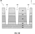
- FIGS. 11A through 11M are simplified partial cross-sectional views illustrating embodiments of a method of forming an apparatus structure, such as one of the memory decks 102 of one of the 3D memory arrays 103 of the memory structure 101 previously described with reference to FIGS. 1 through 3 .
- an apparatus structure such as one of the memory decks 102 of one of the 3D memory arrays 103 of the memory structure 101 previously described with reference to FIGS. 1 through 3 .
- an apparatus structure 200 includes digit lines 202 , digit line contacts 204 on or over the digit lines 202 , a first dielectric material 206 on or over the digit line contacts 204 , a sacrificial dielectric material 208 on or over the first dielectric material 206 , a second dielectric material 210 on or over the sacrificial dielectric material 208 , and a sacrificial material 212 on or over the second dielectric material 210 .
- the digit lines 202 may be formed of and include at least one electrically conductive material, such as one or more of a metal, an alloy, a conductive metal oxide, a conductive metal nitride, a conductive metal silicide, and a conductively doped semiconductor material.
- electrically conductive material such as one or more of a metal, an alloy, a conductive metal oxide, a conductive metal nitride, a conductive metal silicide, and a conductively doped semiconductor material.
- the digit lines 202 may be formed of and include one or more of tungsten (W), tungsten nitride (WN), nickel (Ni), tantalum (Ta), tantalum nitride (TaN), tantalum silicide (TaSi), platinum (Pt), copper (Cu), silver (Ag), gold (Au), aluminum (Al), molybdenum (Mo), titanium (Ti), titanium nitride (TiN), titanium silicide (TiSi), titanium silicon nitride (TiSiN), titanium aluminum nitride (TiAlN), molybdenum nitride (MoN), iridium (Ir), iridium oxide (IrO x ), ruthenium (Ru), ruthenium oxide (RuO x ), and conductively doped silicon.
- the digit lines 202 are formed of and include W.
- Digit line contacts 204 may be formed of and include at least one N-type conductivity material.
- the digit line contacts 204 may serve as drain regions of subsequently formed transistors, as described in further detail below.
- the N-type conductivity material may comprise polysilicon doped with at least one N-type dopant (e.g., arsenic ions, phosphorous ions, antimony ions).
- the first dielectric material 206 may be formed of and include one or more dielectric materials having etch selectivity relative to the sacrificial dielectric material 208 . As described in further detail below, portions of the sacrificial dielectric material 208 may be selectively removed relative to the first dielectric material 206 and the second dielectric material 210 .
- the first dielectric material 206 may comprise an oxide dielectric material, such as one or more of silicon dioxide (SiO 2 ), aluminum oxide (Al 2 O 3 ), phosphosilicate glass, borosilicate glass, borophosphosilicate glass, and fluorosilicate glass. In some embodiments, the first dielectric material 206 comprises SiO 2 .
- the first dielectric material 206 may be substantially undoped, or may doped.
- the sacrificial dielectric material 208 may be formed of and include one or more dielectric materials having etch selectivity relative to the first dielectric material 206 and the second dielectric material 210 .
- the sacrificial dielectric material 208 may comprise a nitride dielectric material, such as silicon nitride (Si 3 N 4 ).
- the sacrificial dielectric material 208 comprises Si 3 N 4 .
- the second dielectric material 210 may be formed of and include one or more dielectric materials having etch selectivity relative to the sacrificial dielectric material 208 .
- the second dielectric material 210 may comprise an oxide dielectric material, such as one or more of SiO 2 , Al 2 O 3 , phosphosilicate glass, borosilicate glass, borophosphosilicate glass, and fluorosilicate glass.
- a material composition of the second dielectric material 210 may be substantially the same as or may be different than that of the first dielectric material 206 .
- the second dielectric material 210 comprises SiO 2 .
- the second dielectric material 210 may be substantially undoped, or may doped.
- the sacrificial material 212 may be formed of and include one or more materials having etch selectivity relative to the second dielectric material 210 . As described in further detail below, portions of the sacrificial material 212 may be selectively removed relative to the second dielectric material 210 .
- the sacrificial material 212 may be formed of and include polysilicon.
- the sacrificial material 212 may be doped, or may be substantially undoped. In some embodiments, the sacrificial material 212 comprises substantially undoped polysilicon.
- openings 214 may be formed in and extend through portions of the sacrificial material 212 , the second dielectric material 210 , the sacrificial dielectric material 208 , and the first dielectric material 206 .
- the openings 214 may vertical extend from an upper surface of the sacrificial material 212 to upper surfaces of the digit line contacts 204 .
- the size, shape, and spacing of each of the openings 214 may at least partially depend upon the size, shape, and spacing structures to be formed within the openings 214 , as described in further detail below.
- the openings 214 each individually exhibit a substantially circular lateral cross-sectional shape. Centers of the openings 214 may be substantially laterally aligned (e.g., in a lateral direction orthogonal to the X-direction shown in FIG. 11B ) with centers of the digit line contacts 204 thereunder.
- channel structures 216 may be formed within the openings 214 .
- each of the channel structures 216 may comprise a container-shaped structure including a floor, and at least one sidewall integral and continuous with the floor and at least defining a void space comprising a remaining (e.g., unfilled) portion of the opening 214 associated with the channel structure 216 .
- the channel structures 216 each include a generally tubular sidewall integral and continuous with a floor. Accordingly, each of the channel structures 216 may exhibit a generally annular lateral cross-sectional shape above the floor thereof.
- dielectric structures 218 made be formed within remaining (e.g., unfilled) portions of the openings 214 ( FIG. 11C ). As shown in FIG. 11D , the dielectric structures 218 may be confined with boundaries (e.g., vertical boundaries, lateral boundaries) of the channel structures 216 . The dielectric structures 218 may exhibit sizes, shapes, and spacing corresponding to those of the void spaces previously defined by the channel structure 216 . In some embodiments, the dielectric structures 218 comprise pillars exhibiting generally circular lateral cross-sectional shapes.
- the dielectric structures 218 may be formed of and include one or more dielectric materials having etch selectivity relative to the sacrificial dielectric material 208 .
- the dielectric structures 218 may comprise an oxide dielectric material, such as one or more of SiO 2 , Al 2 O 3 , phosphosilicate glass, borosilicate glass, borophosphosilicate glass, and fluorosilicate glass.
- a material composition of the dielectric structures 218 may be substantially the same as or may be different than that of one or more (e.g., each) of the first dielectric material 206 and the second dielectric material 210 .
- the dielectric structures 218 are formed of and include SiO 2 .
- the dielectric structures 218 may be formed by non-conformally forming (e.g., non-conformally depositing through a PVD process) a dielectric material (e.g., an oxide dielectric material) on exposed surfaces of the channel structures 216 and the sacrificial material 212 inside and outside of the openings 214 , and then removing (e.g., through an abrasive planarization process, such as a CMP process) portions of the semiconductive material outside of the boundaries (e.g., the vertical boundaries, the lateral boundaries) of the openings 214 .
- a dielectric material e.g., an oxide dielectric material
- capacitor contacts 222 may be formed on exposed upper surfaces of the channel structures 216 and the second dielectric material 210 .
- the capacitor contacts 222 may be positioned laterally adjacent the exposed surfaces of the upper portions of the dielectric structures 218 .
- Each of the capacitor contacts 222 may individually substantially laterally surround one of the dielectric structures 218 .
- the capacitor contacts 222 may serve as source regions of subsequently formed transistors, as described in further detail below.
- the capacitor contacts 222 may be formed of and include at least one N-type conductivity material.
- the N-type conductivity material may comprise polysilicon doped with at least one N-type dopant (e.g., arsenic ions, phosphorous ions, antimony ions).
- a material composition of the capacitor contacts 222 may be substantially the same as or may be different than that of the digit line contacts 204 .
- the capacitor contacts 222 may be formed using conventional processes and conventional processing equipment, which are not described in detail herein.
- an N-type conductivity material may be conformally formed (e.g., deposited through one or more of a PVD process, a CVD process, an ALD process, and a spin-coating process) over exposed surfaces of the dielectric structures 218 , the channel structures 216 , and the second dielectric material 210 , and then an anisotropic etching process may be performed to remove the N-type conductivity material from upper surfaces of the dielectric structures 218 and from portions of the upper surfaces of the second dielectric material 210 , while maintaining the gate material on the upper surfaces of the channel structures 216 and on the sidewalls of the upper portions of the dielectric structures 218 .
- portions of the second dielectric material 210 , the sacrificial dielectric material 208 , and the first dielectric material 206 not covered by the capacitor contacts 222 may be selectively removed to form linear trenches 224 .
- the linear trenches 224 may vertically extend from upper surfaces of the capacitor contacts 222 to one or more locations in the first dielectric material 206 above a lowermost boundary of the first dielectric material 206 .
- the linear trenches 224 may laterally extending a direction substantially orthogonal to a direction (e.g., the X-direction) in which the digit lines 202 .
- the linear trenches 224 may expose portions of the sacrificial dielectric material 208 for subsequent removal, as described in further detail below.
- the capacitor contacts 222 may protect portions of the second dielectric material 210 , the sacrificial dielectric material 208 , and the first dielectric material 206 covered thereby from removal.
- the linear trenches 224 may be formed using conventional processes and conventional processing equipment, which are not described in detail herein.
- the second dielectric material 210 , the sacrificial dielectric material 208 , and the first dielectric material 206 may be exposed to at least one anisotropic etching process (e.g., at least one dry anisotropic etching process, such as at least one of a reactive ion etching (RIE) process, a deep RIE process, a plasma etching process, a reactive ion beam etching process, and a chemically assisted ion beam etching process) to form the linear trenches 224 .
- RIE reactive ion etching
- a third dielectric material 226 may be formed within the linear trenches 224 ( FIG. 11G ).
- the third dielectric material 226 may substantially fill the linear trenches 224 ( FIG. 11G ).
- the third dielectric material 226 may have etch selectivity relative to the sacrificial dielectric material 208 .
- the third dielectric material 226 may comprise an oxide dielectric material, such as one or more of SiO 2 , Al 2 O 3 , phosphosilicate glass, borosilicate glass, borophosphosilicate glass, and fluorosilicate glass.
- a material composition of the third dielectric material 226 may be substantially the same as or may be different than that of one or more (e.g., each) of the first dielectric material 206 , the second dielectric material 210 , and the dielectric structures 218 .
- the third dielectric material 226 is SiO 2 .
- the third dielectric material 226 may be formed using conventional processes and conventional processing equipment, which are not described in detail herein.
- a dielectric material e.g., an oxide dielectric material
- a dielectric material may be non-conformally formed (e.g., non-conformally deposited through a PVD process) on exposed surfaces of the first dielectric material 206 , the sacrificial dielectric material 208 , the second dielectric material 210 , the capacitor contacts 222 , and the dielectric structures 218 , and then portions of the dielectric material outside of the boundaries (e.g., the vertical boundaries, the lateral boundaries) of the linear trenches 224 ( FIG. 11G ) may be removed (e.g., by way of an abrasive planarization process, such as a CMP process).
- an abrasive planarization process such as a CMP process
- portions of the third dielectric material 226 may be removed to form apertures 228 (e.g., vias, open, holes) extending through remaining portions of the third dielectric material 226 ( FIG. 11H ) and exposing portions of the sacrificial dielectric material 208 .
- the apertures 228 expose side surfaces of the sacrificial dielectric material 208 .
- the apertures 228 exhibit geometric configurations (e.g., different sizes, different shapes) than the linear trenches 224 ( FIG. 11G ) within which the third dielectric material 226 ( FIG. 11I ) is formed.
- the apertures 228 may each individually exhibit a generally columnar (e.g., circular columnar) shape. Accordingly, the apertures 228 may be partially laterally surrounded (e.g., in a direction orthogonal to the X-direction shown in FIG. 11I ) by remaining portions of the third dielectric material 226 ( FIG. 11H , omitted from FIG. 11I for clarity and ease of understanding of the drawings and related description with respect to the apertures 228 ). Put another way, some portions of the sidewalls of the sacrificial dielectric material 208 may be exposed by the apertures 228 , while other portions of the sidewalls of the sacrificial dielectric material 208 may remain covered by remaining portions of the third dielectric material 226 .
- the apertures 228 may be formed in the third dielectric material 226 ( FIG. 11I ) using conventional processes, which are not described in detail herein.
- portions (e.g., less than all) of the third dielectric material 226 ( FIG. 11I ) may be subjected to anisotropic etching (e.g., anisotropic dry etching, such as one or more of RIE, deep RIE, plasma etching, reactive ion beam etching, and chemically assisted ion beam etching) to form the apertures 228 .
- anisotropic etching e.g., anisotropic dry etching, such as one or more of RIE, deep RIE, plasma etching, reactive ion beam etching, and chemically assisted ion beam etching
- the sacrificial dielectric material 208 may be selectively removed to form tunnels 230 laterally adjacent the channel structures 216 and linearly extending a direction substantially orthogonal to a direction (e.g., the X-direction) in which the digit lines 202 .
- the tunnels 230 are accessible by way of the apertures 228 (delineated, for clarity and ease of understanding of the drawings and related description, in FIG. 11J from the tunnels 230 by way of dashed lines).
- Portions of the tunnels 230 not directly adjacent the apertures 228 may be substantially surrounded and defined by surfaces of the channel structures 216 , and surfaces of remaining portions of the first dielectric material 206 , the second dielectric material 210 , and the third dielectric material 226 ( FIG. 11H , omitted from FIG. 11J for clarity and ease of understanding of the drawings and related description with respect to the apertures 228 ).
- the sacrificial dielectric material 208 may be selectively removed (e.g., exhumed) by way of the apertures 228 by treating the apparatus structure 200 with at least one etchant (e.g., wet etchant) formulated to selectively remove sacrificial dielectric material 208 ( FIG. 11I ) without substantially removing exposed portions of the channel structures 216 , the capacitor contacts 222 , the first dielectric material 206 , the second dielectric material 210 , the third dielectric material 226 , and the dielectric structures 218 .
- etchant e.g., wet etchant
- the apparatus structure 200 may be exposed to the etchant using conventional processes (e.g., spin-coating process, a spray-coating process, an immersion-coating process, a vapor-coating process, a soaking process, combinations thereof) and conventional processing equipment, which are not described in detail herein.
- conventional processes e.g., spin-coating process, a spray-coating process, an immersion-coating process, a vapor-coating process, a soaking process, combinations thereof
- conventional processing equipment which are not described in detail herein.
- a gate dielectric material 232 may be formed on exposed surfaces of the channel structures 216 , and word lines 234 may be formed within the tunnels 230 ( FIG. 11J ) and the apertures 228 ( FIG. 11J ). The gate dielectric material 232 may laterally intervene between the word lines 234 and the channel structures 216 .
- the gate dielectric material 232 may substantially cover portions of the sidewalls of the channel structures 216 not covered by the first dielectric material 206 , the second dielectric material 210 , the third dielectric material 226 ( FIG. 11H ), and the dielectric structures 218 .
- the gate dielectric material 232 may, for example, comprise an oxide dielectric material, such as one or more of SiO 2 , Al 2 O 3 , hafnium oxide (HfO 2 ), a hafnium silicon oxide (HfSiO x ), an aluminum silicon oxide (AlSiO x ), a phosphosilicate glass, borosilicate glass, borophosphosilicate glass, and fluorosilicate glass.
- a material composition of the gate dielectric material 232 may be substantially the same as or may be different than that of one or more (e.g., each) of the first dielectric material 206 , the second dielectric material 210 , the third dielectric material 226 ( FIG. 11H ), and the dielectric structures 218 .
- the gate dielectric material 232 is SiO 2 .
- the gate dielectric material 232 may be formed using conventional processes and conventional processing equipment, which are not described in detail herein.
- the gate dielectric material 232 may be grown (e.g., epitaxially grown) on the channel structures 216 through a thermal oxidation process.
- the thermal oxidation process may include exposing the channel structures 216 to at least one oxidizing agent at a temperature within a range of from about 800° C. to about 1200° C.
- the word lines 234 may substantially (e.g., completely) fill portions of the tunnels 230 ( FIG. 11J ) not occupied by the gate dielectric material 232 , and may also partially (e.g., less than completely) fill the apertures 228 . As shown in FIG. 11K , the word lines 234 may include elevated portions 236 and recessed portions 238 . The elevated portions 236 may be located (e.g., confined) within the tunnels 230 ( FIG. 11J ) may be laterally extend in a direction substantially orthogonal to a direction (e.g., the X-direction) in which the digit lines 202 laterally extend.
- the recessed portions 238 may located (e.g., confined) within the apertures 228 , laterally extend (e.g., in the X-direction) from and between the elevated portions 236 .
- the elevated portions 236 of the word lines 234 are delineated, for clarity and ease of understanding of the drawings and related description, from the recessed portions 238 of the word lines 234 by way of dashed lines.
- the elevated portions 236 and the recessed portions 238 of the word lines 234 are formed to be integral and continuous with another.
- the word lines 234 may be formed of and include at least one electrically conductive material, such as one or more of a metal, an alloy, a conductive metal oxide, a conductive metal nitride, a conductive metal silicide, and a conductively doped semiconductor material.
- the word lines 234 may be formed of and include one or more of W, WN, Ni, Ta, TaN, TaSi, Pt, Cu, Ag, Au, Al, Mo, Ti, TiN, TiSi, TiSiN, TiAlN, MoN, Ir, IrO x , Ru, RuO x , and conductively doped silicon.
- a material composition of the word lines 234 may be substantially the same as or may be different than that of the digit lines 202 .
- the word lines 234 are formed of and include TiN.
- the word lines 234 may be formed using conventional processes (e.g., conventional material deposition processes, conventional material removal processes) and conventional processing equipment, which are not described in detail herein.
- an electrically conductive material may be deposited within the tunnels 230 ( FIG. 11J ) and the apertures 228 using one or more of a PVD process, a CVD process, and an ALD process.
- the digit line contacts 204 , the channel structures 216 , the capacitor contacts 222 , the gate dielectric material 232 , and the word lines 234 may form transistors 240 of the apparatus structure 200 .
- the transistors 240 may correspond to the first transistors 120 A ( FIG. 3 ) or the second transistors 120 B ( FIG. 3 ) of the memory cells 120 ( FIG. 3 ) of one of memory decks 102 ( FIG. 3 ) of the apparatus 100 previously described with reference to FIGS. 1 through 3 .
- the apparatus structure 200 may be subjected to additional processing to form the addition components (e.g., the other of the first transistors 120 A and the second transistors 120 B; the capacitors 120 C) of the memory cells 120 ( FIG. 3 ), as described in further detail below.
- a fourth dielectric material 242 may be formed within remaining (e.g., unfilled) portions of the apertures 228 ( FIG. 11K ).
- the fourth dielectric material 242 may substantially fill the remaining portions of the apertures 228 ( FIG. 11K ).
- the fourth dielectric material 242 may, for example, comprise an oxide dielectric material, such as one or more of SiO 2 , Al 2 O 3 , HfO 2 , HfSiO x , AlSiO x , a phosphosilicate glass, borosilicate glass, borophosphosilicate glass, and fluorosilicate glass.
- a material composition of the fourth dielectric material 242 may be substantially the same as or may be different than that of one or more (e.g., each) of the first dielectric material 206 , the second dielectric material 210 , the third dielectric material 226 , and the dielectric structures 218 .
- the fourth dielectric material 242 is SiO 2 .
- the fourth dielectric material 242 may be formed using conventional processes and conventional processing equipment, which are not described in detail herein.
- a dielectric material e.g., an oxide dielectric material
- a dielectric material may be non-conformally formed (e.g., non-conformally deposited through a PVD process) on exposed surfaces of the word lines 234 , the second dielectric material 210 , the capacitor contacts 222 , and the dielectric structures 218 , and then portions of the dielectric material outside of the boundaries (e.g., the vertical boundaries, the lateral boundaries) of the apertures 228 ( FIG. 11K ) may be removed (e.g., by way of an abrasive planarization process, such as a CMP process).
- an abrasive planarization process such as a CMP process
- the apparatus structure 200 may, optionally, be formed to include p-well contacts 243 laterally extending from and between channel structures 216 of laterally-neighboring transistors 240 .
- the p-well contacts 243 may be formed of and include at least one P-type conductivity material.
- the P-type conductivity material may comprise polysilicon doped with at least one P-type dopant (e.g., boron ions).
- the p-well contacts 243 may be formed by forming (e.g., through convention material removal and material deposition processes) a pattern (e.g., an X-shaped pattern) of intersecting P-type conductivity spacers within the sacrificial dielectric material 208 ( FIG. 11A ) and then proceeding with the method steps previously described with reference to FIGS. 11B through 11L . Portions of the P-type conductivity material remaining within the remaining portions of the sacrificial dielectric material 208 ( FIG. 11B ) following the formation of the openings 214 ( FIG.
- the apparatus structure 200 may be subjected to additional processing to form an array of memory cells including the transistors 240 .
- capacitors 244 may be formed vertically over and in electrical communication with the capacitor contacts 222 of the transistors 240 , and then additional transistors 240 ′ may be formed vertically over and in electrical communication with the capacitors 244 .
- the capacitors 244 may be laterally separated from one another by a fifth dielectric material 246 (e.g., an oxide dielectric material) having a material composition substantially similar to or different than that of one or more of the first dielectric material 206 , the second dielectric material 210 , the third dielectric material 226 , the fourth dielectric material 242 , and the dielectric structures 218 .
- the transistors 240 , the capacitors 244 , and the additional transistors 240 ′ may form memory cells 248 corresponding to the memory cells 120 previously described herein with reference to FIG. 3 .
- the transistors 240 may correspond to (e.g., be employed as) the first transistors 120 A ( FIG.
- the capacitors 244 may correspond to the capacitors 120 C, and the additional transistors 240 ′ may correspond to the second transistors 120 B.
- the apparatus structure 200 may, for example, correspond to one of the memory decks 102 of one of the 3D memory arrays 103 of the memory structure 101 of the apparatus 100 previously described with reference to FIGS. 1 through 3 .
- FIG. 11N a feature designated by a reference numeral that as a prime (′) of a reference numeral of a previously-described feature will be understood to be substantially similar to the previously-described feature and will also be understood to be formed in substantially the same manner as the previously-described feature.
- an additional first dielectric material 206 ′, an additional second dielectric material 210 ′, an additional fourth dielectric material 242 ′, additional dielectric structures 218 ′, additional channel structures 216 ′, and additional word lines 234 ′ may respectively be substantially similar to and may formed in substantially the same manner as the first dielectric material 206 , the second dielectric material 210 , the fourth dielectric material 242 , the dielectric structures 218 , the channel structures 216 , and the word lines 234 previously described with reference to FIGS. 12A through 12L . As shown in FIG.
- additional capacitor contacts 222 ′ of the additional transistors 240 ′ may exhibit different geometric configurations than the capacitor contacts 222 of the transistors 240 as a result of the different arrangement of the additional transistors 240 ′ relative to the capacitors 244 , as may additional digit line contacts 204 ′ (e.g., geometric configuration more similar to the capacitor contacts 222 ) of the additional transistors 240 ′.
- the additional capacitor contacts 222 ′ of the additional transistors 240 ′ may be formed through conventional processes, and may serve substantially the same function as the capacitor contacts 222 of the transistors 240 .
- additional digit line contacts 204 ′ of the additional transistors 240 ′ may be formed in substantially the same manner as the capacitor contacts 222 of the transistors 240 , and may serve substantially the same function as the digit line contacts 204 of the transistors 240 .
- Additional digit lines 202 ′ may be substantially similar to the digit lines 202 , and may be formed over the additional digit line contacts 204 ′ through processes substantially similar to those employed to form the digit lines 202 .
- a method of forming an apparatus comprises forming a stack structure comprising digit lines, digit line contacts over the digit lines, a first dielectric material over the digit line contacts, a sacrificial dielectric material over the first dielectric material, a second dielectric material over the sacrificial dielectric material, and a sacrificial material over the second dielectric material.
- Channel structures are formed to vertically extend from an upper surface of the sacrificial material to upper surfaces of the digit line contacts, each of the channel structures comprising a generally tubular sidewall integral and continuous with a floor. Portions of the sacrificial material and the channel structures above upper boundaries of the second dielectric material are removed.
- Capacitor contacts are formed on exposed upper surfaces of the channel structures and the second dielectric material.
- Linear trenches are formed between the capacitor contacts, the linear trenches vertically extending from upper surfaces of the capacitors contacts to the first dielectric material and laterally extending substantially orthogonal to a direction of the digit lines.
- the linear trenches are formed with a third dielectric material. Portions of the third dielectric material are removed to form apertures exposing portions of the sacrificial dielectric material. Portions of the sacrificial dielectric material are removed to form tunnels laterally extending substantially orthogonal to the direction of the digit lines. Word lines are formed within the tunnels and lower portions of the apertures.
- FIG. 12 is a block diagram of an illustrative electronic system 300 according to embodiments of disclosure.
- the electronic system 300 may comprise, for example, a computer or computer hardware component, a server or other networking hardware component, a cellular telephone, a digital camera, a personal digital assistant (PDA), portable media (e.g., music) player, a Wi-Fi or cellular-enabled tablet such as, for example, an iPad® or SURFACE® tablet, an electronic book, a navigation device, etc.
- PDA personal digital assistant
- the electronic system 300 includes at least one memory device 302 (e.g., at least one DRAM device).
- the memory device 302 may comprise, for example, an embodiment of one or more of an apparatus structure (e.g., the apparatus structure 200 ) and an apparatus (e.g., the apparatus 100 ) previously described herein.
- the electronic system 300 may further include at least one electronic signal processor device 304 (often referred to as a “microprocessor”).
- the electronic signal processor device 304 may, optionally, include an embodiment of an apparatus structure (e.g., the apparatus structure 200 ) and an apparatus (e.g., the apparatus 100 ) previously described herein.
- the electronic system 300 may further include one or more input devices 306 for inputting information into the electronic system 300 by a user, such as, for example, a mouse or other pointing device, a keyboard, a touchpad, a button, or a control panel.
- the electronic system 300 may further include one or more output devices 308 for outputting information (e.g., visual or audio output) to a user such as, for example, a monitor, a display, a printer, an audio output jack, a speaker, etc.
- the input device 306 and the output device 308 may comprise a single touchscreen device that can be used both to input information to the electronic system 300 and to output visual information to a user.
- the input device 306 and the output device 308 may communicate electrically with one or more of the memory device 302 and the electronic signal processor device 304 .
- an electronic system comprises an input device, an output device, a processor device operably coupled to the input device and the output device, and a memory device operably coupled to the processor device.
- the memory device comprises a base structure, a memory structure, odd digit line interconnect structures, even digit line interconnect structures, odd word line interconnect structures, and even word line interconnect structures.
- the base structure comprises odd sense amplifier regions, even sense amplifier regions, odd word line driver regions, and even word line driver regions.
- the memory structure overlies the base structure and comprises memory decks.
- the memory decks each comprise digit lines, additional digit lines, memory cells, and word lines.
- the digit lines comprise odd digit lines and even digit lines laterally alternating with the odd digit lines.
- the additional digit lines comprise additional odd digit lines and additional even digit lines laterally alternating with the additional odd digit lines.
- the memory cells are vertically between and electrically connected to the digit lines and the additional digit lines. Each memory cell comprises a lower transistor, an upper transistor, and a capacitor vertically between the lower transistor and the upper transistor.
- the word lines are electrically electrical connected to the memory cells and laterally extend orthogonal to the digit lines.
- the word lines comprise odd word lines and even word lines laterally alternating with the odd word lines.
- the odd digit line interconnect structures electrically connect the odd sense amplifier regions of the base structure to the odd digit lines and the additional odd digit lines of the memory structure.
- the even digit line interconnect structures electrically connect the even sense amplifier regions of the base structure to the even digit lines and the additional even digit lines of the memory structure.
- the odd word line interconnect structures electrically connect the odd word line driver regions of the base structure to the odd word lines of the memory structure.
- the even word line interconnect structures electrically connect the even word line driver regions of the base structure to the even word lines of the memory structure.
- the devices, structures, and methods of the disclosure advantageously facilitate improved apparatus (e.g., semiconductor device; memory device, such as DRAM device) performance, reduced costs (e.g., manufacturing costs, material costs), increased miniaturization of components, and greater packaging density as compared to conventional devices, conventional structures, and conventional methods.
- the devices, structures, and methods of the disclosure may also improve performance, scalability, efficiency, and simplicity as compared to conventional devices, conventional structures, and conventional methods.
Landscapes
- Engineering & Computer Science (AREA)
- Microelectronics & Electronic Packaging (AREA)
- Computer Hardware Design (AREA)
- Manufacturing & Machinery (AREA)
- Physics & Mathematics (AREA)
- Geometry (AREA)
- Semiconductor Memories (AREA)
Abstract
Description
Claims (26)
Priority Applications (1)
| Application Number | Priority Date | Filing Date | Title |
|---|---|---|---|
| US16/212,418 US10790286B2 (en) | 2018-12-06 | 2018-12-06 | Apparatuses including 3D memory arrays, methods of forming the apparatuses, and related electronic systems |
Applications Claiming Priority (1)
| Application Number | Priority Date | Filing Date | Title |
|---|---|---|---|
| US16/212,418 US10790286B2 (en) | 2018-12-06 | 2018-12-06 | Apparatuses including 3D memory arrays, methods of forming the apparatuses, and related electronic systems |
Publications (2)
| Publication Number | Publication Date |
|---|---|
| US20200185385A1 US20200185385A1 (en) | 2020-06-11 |
| US10790286B2 true US10790286B2 (en) | 2020-09-29 |
Family
ID=70971892
Family Applications (1)
| Application Number | Title | Priority Date | Filing Date |
|---|---|---|---|
| US16/212,418 Active 2039-02-19 US10790286B2 (en) | 2018-12-06 | 2018-12-06 | Apparatuses including 3D memory arrays, methods of forming the apparatuses, and related electronic systems |
Country Status (1)
| Country | Link |
|---|---|
| US (1) | US10790286B2 (en) |
Cited By (5)
| Publication number | Priority date | Publication date | Assignee | Title |
|---|---|---|---|---|
| US11069385B1 (en) * | 2020-03-31 | 2021-07-20 | Micron Technology, Inc. | Integrated assemblies comprising folded-digit-line-configurations |
| US11152056B1 (en) * | 2020-09-14 | 2021-10-19 | Micron Technology, Inc. | Integrated assemblies |
| US11410980B2 (en) | 2018-12-07 | 2022-08-09 | Micron Technology, Inc. | Integrated assemblies comprising vertically-stacked decks |
| US11900989B2 (en) | 2019-04-09 | 2024-02-13 | Micron Technology, Inc. | Memory array with multiplexed digit lines |
| US20240290374A1 (en) * | 2023-02-24 | 2024-08-29 | Micron Technology, Inc. | Microelectronic devices, and related memory devices and electronic systems |
Families Citing this family (8)
| Publication number | Priority date | Publication date | Assignee | Title |
|---|---|---|---|---|
| US11538808B2 (en) | 2018-09-07 | 2022-12-27 | Intel Corporation | Structures and methods for memory cells |
| US20220189957A1 (en) * | 2020-12-10 | 2022-06-16 | Intel Corporation | Transistors, memory cells, and arrangements thereof |
| US12148734B2 (en) * | 2020-12-10 | 2024-11-19 | Intel Corporation | Transistors, memory cells, and arrangements thereof |
| US11849578B2 (en) | 2021-07-29 | 2023-12-19 | Sandisk Technologies Llc | Three-dimensional memory device with a columnar memory opening arrangement and method of making thereof |
| US12471289B2 (en) | 2021-12-22 | 2025-11-11 | Intel Corporation | Diagonal memory with vertical transistors and wrap-around control lines |
| CN117479527A (en) * | 2022-09-21 | 2024-01-30 | 北京超弦存储器研究院 | A storage structure, electronic device |
| US20240407151A1 (en) * | 2023-05-30 | 2024-12-05 | Macronix International Co., Ltd. | Memory cell circuit, memory cell array structure and manufacturing method thereof |
| CN120712916A (en) * | 2024-01-24 | 2025-09-26 | 长江存储科技有限责任公司 | Semiconductor device and method for manufacturing the same |
Citations (15)
| Publication number | Priority date | Publication date | Assignee | Title |
|---|---|---|---|---|
| US4920517A (en) | 1986-04-24 | 1990-04-24 | Matsushita Electric Industrial Co., Ltd. | Semiconductor memory device having sub bit lines |
| US6043562A (en) * | 1996-01-26 | 2000-03-28 | Micron Technology, Inc. | Digit line architecture for dynamic memory |
| US6075737A (en) | 1998-12-02 | 2000-06-13 | Micron Technology, Inc. | Row decoded biasing of sense amplifier for improved one's margin |
| US6504756B2 (en) | 1998-04-08 | 2003-01-07 | Micron Technology, Inc. | Dual floating gate programmable read only memory cell structure and method for its fabrication and operation |
| US20030223292A1 (en) | 2002-05-16 | 2003-12-04 | Hasan Nejad | Stacked 1T-nmemory cell structure |
| US20090207681A1 (en) * | 2008-02-19 | 2009-08-20 | Micron Technology, Inc. | Systems and devices including local data lines and methods of using, making, and operating the same |
| US20090238010A1 (en) | 2008-03-20 | 2009-09-24 | Micron Technology, Inc. | Systems and devices including multi-transistor cells and methods of using, making, and operating the same |
| US20110267912A1 (en) | 2008-03-10 | 2011-11-03 | Micron Technology, Inc. | Digit line equilibration using access devices at the edge of sub arrays |
| US20140117507A1 (en) | 2012-10-30 | 2014-05-01 | Globalfoundries Inc. | Double trench well formation in sram cells |
| US8872247B2 (en) * | 2009-11-04 | 2014-10-28 | Micron Technology, Inc. | Memory cells having a folded digit line architecture |
| US9190494B2 (en) | 2008-02-19 | 2015-11-17 | Micron Technology, Inc. | Systems and devices including fin field-effect transistors each having U-shaped semiconductor fin |
| US9715918B1 (en) | 2016-05-23 | 2017-07-25 | Micron Technology, Inc. | Power reduction for a sensing operation of a memory cell |
| US9773728B1 (en) | 2016-12-27 | 2017-09-26 | Micron Technology, Inc. | Memory arrays |
| US20170278559A1 (en) * | 2016-03-28 | 2017-09-28 | Micron Technology, Inc. | Apparatuses and methods for data movement |
| US9847337B1 (en) | 2016-12-27 | 2017-12-19 | Micron Technology, Inc. | Memory arrays comprising ferroelectric capacitors |
-
2018
- 2018-12-06 US US16/212,418 patent/US10790286B2/en active Active
Patent Citations (15)
| Publication number | Priority date | Publication date | Assignee | Title |
|---|---|---|---|---|
| US4920517A (en) | 1986-04-24 | 1990-04-24 | Matsushita Electric Industrial Co., Ltd. | Semiconductor memory device having sub bit lines |
| US6043562A (en) * | 1996-01-26 | 2000-03-28 | Micron Technology, Inc. | Digit line architecture for dynamic memory |
| US6504756B2 (en) | 1998-04-08 | 2003-01-07 | Micron Technology, Inc. | Dual floating gate programmable read only memory cell structure and method for its fabrication and operation |
| US6075737A (en) | 1998-12-02 | 2000-06-13 | Micron Technology, Inc. | Row decoded biasing of sense amplifier for improved one's margin |
| US20030223292A1 (en) | 2002-05-16 | 2003-12-04 | Hasan Nejad | Stacked 1T-nmemory cell structure |
| US9190494B2 (en) | 2008-02-19 | 2015-11-17 | Micron Technology, Inc. | Systems and devices including fin field-effect transistors each having U-shaped semiconductor fin |
| US20090207681A1 (en) * | 2008-02-19 | 2009-08-20 | Micron Technology, Inc. | Systems and devices including local data lines and methods of using, making, and operating the same |
| US20110267912A1 (en) | 2008-03-10 | 2011-11-03 | Micron Technology, Inc. | Digit line equilibration using access devices at the edge of sub arrays |
| US20090238010A1 (en) | 2008-03-20 | 2009-09-24 | Micron Technology, Inc. | Systems and devices including multi-transistor cells and methods of using, making, and operating the same |
| US8872247B2 (en) * | 2009-11-04 | 2014-10-28 | Micron Technology, Inc. | Memory cells having a folded digit line architecture |
| US20140117507A1 (en) | 2012-10-30 | 2014-05-01 | Globalfoundries Inc. | Double trench well formation in sram cells |
| US20170278559A1 (en) * | 2016-03-28 | 2017-09-28 | Micron Technology, Inc. | Apparatuses and methods for data movement |
| US9715918B1 (en) | 2016-05-23 | 2017-07-25 | Micron Technology, Inc. | Power reduction for a sensing operation of a memory cell |
| US9773728B1 (en) | 2016-12-27 | 2017-09-26 | Micron Technology, Inc. | Memory arrays |
| US9847337B1 (en) | 2016-12-27 | 2017-12-19 | Micron Technology, Inc. | Memory arrays comprising ferroelectric capacitors |
Cited By (7)
| Publication number | Priority date | Publication date | Assignee | Title |
|---|---|---|---|---|
| US11410980B2 (en) | 2018-12-07 | 2022-08-09 | Micron Technology, Inc. | Integrated assemblies comprising vertically-stacked decks |
| US12249598B2 (en) | 2018-12-07 | 2025-03-11 | Micron Technology, Inc. | Integrated assemblies comprising vertically-stacked decks with interconnected conductive lines |
| US11900989B2 (en) | 2019-04-09 | 2024-02-13 | Micron Technology, Inc. | Memory array with multiplexed digit lines |
| US11069385B1 (en) * | 2020-03-31 | 2021-07-20 | Micron Technology, Inc. | Integrated assemblies comprising folded-digit-line-configurations |
| US11152056B1 (en) * | 2020-09-14 | 2021-10-19 | Micron Technology, Inc. | Integrated assemblies |
| US20240290374A1 (en) * | 2023-02-24 | 2024-08-29 | Micron Technology, Inc. | Microelectronic devices, and related memory devices and electronic systems |
| US12603123B2 (en) * | 2023-02-24 | 2026-04-14 | Micron Technology, Inc. | Microelectronic devices including a control circuitry structure bonded to a memory array structure |
Also Published As
| Publication number | Publication date |
|---|---|
| US20200185385A1 (en) | 2020-06-11 |
Similar Documents
| Publication | Publication Date | Title |
|---|---|---|
| US10790286B2 (en) | Apparatuses including 3D memory arrays, methods of forming the apparatuses, and related electronic systems | |
| US12040041B2 (en) | Control logic assemblies | |
| US8669144B2 (en) | Methods of forming memory arrays | |
| US8859363B2 (en) | Semiconductor devices including vertical channel transistors and methods of fabricating the same | |
| US9070640B2 (en) | Method of forming fine patterns of semiconductor device | |
| US11437318B2 (en) | Microelectronic devices including staircase structures, and related memory devices and electronic systems | |
| US11688689B2 (en) | Electronic devices including stair step structures, and related memory devices, systems, and methods | |
| US11424184B2 (en) | Methods of forming microelectronic devices, and related microelectronic devices, memory devices, and electronic systems | |
| US11908932B2 (en) | Apparatuses comprising vertical transistors having gate electrodes at least partially recessed within channel regions, and related methods and systems | |
| US20240244820A1 (en) | Microelectronic devices, and related memory devices, and electronic systems | |
| US20240074142A1 (en) | Microelectronic devices, related memory devices, electronic systems, and methods | |
| US20260040577A1 (en) | Microelectronic devices, and related methods of forming microelectronic devices | |
| US20250048618A1 (en) | Microelectronic devices, and related methods, memory devices, and electronic systems | |
| US20240334700A1 (en) | Microelectronic devices including vertical planar memory cell structures, and related memory devices and electronic systems | |
| US20240196606A1 (en) | Microelectronic devices including stadium structures, and related memory devices and electronic systems | |
| US20250061936A1 (en) | Microelectronic devices and memory devices including vertically spaced transistors and storage devices, and related electronic systems | |
| US20240315009A1 (en) | Semiconductor memory device |
Legal Events
| Date | Code | Title | Description |
|---|---|---|---|
| AS | Assignment |
Owner name: MICRON TECHNOLOGY, INC., IDAHO Free format text: ASSIGNMENT OF ASSIGNORS INTEREST;ASSIGNOR:JUENGLING, WERNER;REEL/FRAME:047698/0462 Effective date: 20181206 |
|
| FEPP | Fee payment procedure |
Free format text: ENTITY STATUS SET TO UNDISCOUNTED (ORIGINAL EVENT CODE: BIG.); ENTITY STATUS OF PATENT OWNER: LARGE ENTITY |
|
| AS | Assignment |
Owner name: JPMORGAN CHASE BANK, N.A., AS COLLATERAL AGENT, ILLINOIS Free format text: SUPPLEMENT NO. 3 TO PATENT SECURITY AGREEMENT;ASSIGNOR:MICRON TECHNOLOGY, INC.;REEL/FRAME:048951/0902 Effective date: 20190416 Owner name: MORGAN STANLEY SENIOR FUNDING, INC., AS COLLATERAL AGENT, MARYLAND Free format text: SUPPLEMENT NO. 12 TO PATENT SECURITY AGREEMENT;ASSIGNOR:MICRON TECHNOLOGY, INC.;REEL/FRAME:048948/0677 Effective date: 20190416 |
|
| AS | Assignment |
Owner name: MICRON TECHNOLOGY, INC., IDAHO Free format text: RELEASE BY SECURED PARTY;ASSIGNOR:MORGAN STANLEY SENIOR FUNDING, INC., AS COLLATERAL AGENT;REEL/FRAME:050724/0392 Effective date: 20190731 |
|
| AS | Assignment |
Owner name: MICRON TECHNOLOGY, INC., IDAHO Free format text: RELEASE BY SECURED PARTY;ASSIGNOR:JPMORGAN CHASE BANK, N.A., AS COLLATERAL AGENT;REEL/FRAME:051041/0317 Effective date: 20190731 |
|
| STPP | Information on status: patent application and granting procedure in general |
Free format text: AWAITING TC RESP, ISSUE FEE PAYMENT VERIFIED |
|
| STCF | Information on status: patent grant |
Free format text: PATENTED CASE |
|
| CC | Certificate of correction | ||
| MAFP | Maintenance fee payment |
Free format text: PAYMENT OF MAINTENANCE FEE, 4TH YEAR, LARGE ENTITY (ORIGINAL EVENT CODE: M1551); ENTITY STATUS OF PATENT OWNER: LARGE ENTITY Year of fee payment: 4 |