US10777423B2 - Chemical mechanical polishing method - Google Patents
Chemical mechanical polishing method Download PDFInfo
- Publication number
- US10777423B2 US10777423B2 US16/003,111 US201816003111A US10777423B2 US 10777423 B2 US10777423 B2 US 10777423B2 US 201816003111 A US201816003111 A US 201816003111A US 10777423 B2 US10777423 B2 US 10777423B2
- Authority
- US
- United States
- Prior art keywords
- region
- polishing slurry
- contact angle
- surfactant
- cmp
- Prior art date
- Legal status (The legal status is an assumption and is not a legal conclusion. Google has not performed a legal analysis and makes no representation as to the accuracy of the status listed.)
- Active
Links
Images


Classifications
-
- H01L21/3212—
-
- H—ELECTRICITY
- H10—SEMICONDUCTOR DEVICES; ELECTRIC SOLID-STATE DEVICES NOT OTHERWISE PROVIDED FOR
- H10P—GENERIC PROCESSES OR APPARATUS FOR THE MANUFACTURE OR TREATMENT OF DEVICES COVERED BY CLASS H10
- H10P52/00—Grinding, lapping or polishing of wafers, substrates or parts of devices
- H10P52/40—Chemomechanical polishing [CMP]
- H10P52/403—Chemomechanical polishing [CMP] of conductive or resistive materials
-
- H01L21/28—
-
- H01L21/31053—
-
- H—ELECTRICITY
- H10—SEMICONDUCTOR DEVICES; ELECTRIC SOLID-STATE DEVICES NOT OTHERWISE PROVIDED FOR
- H10D—INORGANIC ELECTRIC SEMICONDUCTOR DEVICES
- H10D64/00—Electrodes of devices having potential barriers
- H10D64/01—Manufacture or treatment
- H10D64/011—Manufacture or treatment of electrodes ohmically coupled to a semiconductor
-
- H—ELECTRICITY
- H10—SEMICONDUCTOR DEVICES; ELECTRIC SOLID-STATE DEVICES NOT OTHERWISE PROVIDED FOR
- H10P—GENERIC PROCESSES OR APPARATUS FOR THE MANUFACTURE OR TREATMENT OF DEVICES COVERED BY CLASS H10
- H10P95/00—Generic processes or apparatus for manufacture or treatments not covered by the other groups of this subclass
- H10P95/06—Planarisation of inorganic insulating materials
- H10P95/062—Planarisation of inorganic insulating materials involving a dielectric removal step
Definitions
- CMP Chemical mechanical polishing
- FIG. 1A , FIG. 1B and FIG. 1C are schematic cross-sectional views illustrating a chemical mechanical polishing (CMP) method in accordance with some embodiments of the present disclosure.
- CMP chemical mechanical polishing
- FIG. 2 is a flowchart illustrating a method for planarizing a substrate in accordance with various aspects of the present disclosure.
- FIG. 3 is a flowchart illustrating a chemical mechanical polishing (CMP) method in accordance with various aspects of the present disclosure.
- FIG. 4 , FIG. 5 and FIG. 6 are schematic diagrams of a planarization method in accordance with various aspects of some embodiments of the present disclosure.
- FIG. 7 , FIG. 7A and FIG. 8 are schematic diagrams of a planarization method in accordance with various aspects of some embodiments of the present disclosure.
- FIG. 9 , FIG. 9A and FIG. 10 are schematic diagrams of a planarization method in accordance with various aspects of some embodiments of the present disclosure.
- FIG. 11A , FIG. 11B , FIG. 11C and FIG. 11D are schematic cross-sectional views illustrating a CMP method in accordance with some embodiments of the present disclosure.
- first and second features are formed in direct contact
- additional features may be formed between the first and second features, such that the first and second features may not be in direct contact
- present disclosure may repeat reference numerals and/or letters in the various examples. This repetition is for the purpose of simplicity and clarity and does not in itself dictate a relationship between the various embodiments and/or configurations discussed.
- spatially relative terms such as “beneath,” “below,” “lower,” “above,” “upper,” “on” and the like, may be used herein for ease of description to describe one element or feature's relationship to another element(s) or feature(s) as illustrated in the figures.
- the spatially relative terms are intended to encompass different orientations of the device in use or operation in addition to the orientation depicted in the figures.
- the apparatus may be otherwise oriented (rotated 90 degrees or at other orientations) and the spatially relative descriptors used herein may likewise be interpreted accordingly.
- first and second describe various elements, components, regions, layers and/or sections, these elements, components, regions, layers and/or sections should not be limited by these terms. These terms may be only used to distinguish one element, component, region, layer or section from another.
- the terms such as “first” and “second” when used herein do not imply a sequence or order unless clearly indicated by the context.
- the term “substantially” refers to the complete or nearly complete extent or degree of an action, characteristic, property, state, structure, item, or result.
- a surface that is “substantially” coplanar with another surface would mean that these two surfaces are either completely located in the same plane or nearly completely located in the same plane.
- the exact allowable degree of deviation from absolute completeness may in some cases depend on the specific context. However, generally speaking the nearness of completion will be so as to have the same overall result as if absolute and total completion is obtained.
- polishing slurry refers to include an aqueous mixture having a chemical composition that may enhance, reduce, or otherwise modify a substrate polishing rate.
- the polishing slurry may also include polishing abrasives, chemical reagents and other additives.
- the term “contact angle” is defined as the angle formed by a drop of liquid in contact with the surface of the substrate.
- the value of the contact angle indicates the degree of hydrophobicity or hydrophilicity of the substrate. In some cases, when the contact angle is equal to or greater than 90 degrees, the substrate is hydrophobic. When the contact angle is less than 90 degrees, the substrate is hydrophilic.
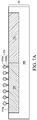
- FIG. 1A , FIG. 1B and FIG. 1C are schematic cross-sectional views illustrating a chemical mechanical polishing (CMP) method in accordance with some embodiments of the present disclosure.
- CMP chemical mechanical polishing
- a semiconductor structure 10 is provided.
- the semiconductor structure 10 includes a substrate 100 , a first material 102 and a second material 104 .
- the first material 102 and the second material 104 have different degrees of hydrophobicity or hydrophilicity.
- the first material 102 may be configured as dielectric layer, and the second material 104 may be configured as conductive vias.
- the second material 104 over the first material 102 may need to be removed to form a plurality of separated conductive vias, and the surface of the first material 102 and the second material 104 may need to be planarized for successive operations.
- a polishing slurry 120 may be dispensed over the semiconductor structure 10 , and a CMP operation may be performed to remove the second material 104 over the first material 102 .
- the abrasives of the polishing slurry 120 may be uniformly distributed over the second material 104 , and the polishing rate is substantially uniform throughout the second material 104 at the beginning of the CMP operation.
- first region 110 and a second region 111 formed from different materials will be formed.
- the first region 110 and the second region 111 have different degrees of hydrophobicity or hydrophilicity.
- the first region 110 is a hydrophobic region and the second region 111 is a hydrophilic region.
- the hydrophobic first region 110 includes a hydrophobic surface 110 a and the hydrophilic second region 111 includes a hydrophilic surface 111 a . Due to the different degrees of hydrophobicity or hydrophilicity between the first region 110 and the second region 111 , the polishing slurry 120 are tended to approach and concentrate on the hydrophilic surface 111 a than on the hydrophobic surface 110 a.
- the polishing rate in the hydrophilic second region 111 with more polishing slurry 120 is higher than the polishing rate in the hydrophobic first region 110 with less polishing slurry 120 , and therefore the concentrated polishing slurry 120 may cause dishing in the hydrophilic region 111 during the CMP operation.
- a planarization method is provided to mitigate dishing of the substrate or the overlying layer(s) on the substrate.
- the method may include a surface treatment by adding a pH adjuster, a surfactant or a corrosion inhibitor to the polishing slurry.
- the pH adjuster may modify the polishing slurry 120 to an alkaline or an acidic condition, which may help to transform a material of the hydrophobic region into another hydrophilic material.
- the surfactant or the corrosion inhibitor are configured to selectively bonded to the surface of one of the hydrophobic region and the hydrophilic region to alter the degree of hydrophobicity or hydrophilicity, and thus may render its degree of hydrophilicity of the hydrophobic region similar to that of the surface of the other one of the hydrophobic region and the hydrophilic region.
- the surfactant or the corrosion inhibitor tends to bond to one of the hydrophobic region and the hydrophilic region than to the other one of the hydrophobic region and the hydrophilic region by ionic bond, hydrogen bond or the like. Therefore, the polishing slurry will be uniformly dispersed on the hydrophobic region and the hydrophilic region such that dishing can be mitigated.
- a planarizing method is disclosed.
- a substrate is polished by a planarizing method 200 .
- the method 200 includes a number of operations, and the description and illustration are not deemed as a limitation as the sequence of the operations.
- FIG. 2 is a flowchart illustrating a method for planarizing a substrate in accordance with various aspects of the present disclosure.
- the method 200 begins with operation 210 in which a substrate is provided, wherein a surface of the substrate includes a first region and a second region having different degrees of hydrophobicity or hydrophilicity.
- the method 200 continues with operation 220 in which a surface treatment is performed to the first region to render the degree of hydrophobicity or hydrophilicity of the first region in proximity to the degree of hydrophobicity or hydrophilicity of the second region.
- the method 200 proceeds with operation 230 in which the surface of the substrate is polished using a polishing slurry to planarize the surface of the substrate.
- the method 200 is merely an example, and is not intended to limit the present disclosure beyond what is explicitly recited in the claims. Additional operations can be provided before, during, and after the method 200 , and some operations described can be replaced, eliminated, or moved around for additional embodiments of the method.
- the surface treatment is performed by transforming a material of the first region into another material having a degree of hydrophobicity or hydrophilicity similar to a degree of hydrophobicity or hydrophilicity of a material of the second region.
- the material of the first region is transformed into another material by adding a pH adjuster to the polishing slurry.
- the pH adjuster may help to modify the polishing slurry to an alkaline or an acidic condition, which may help to transform the original material of the first region into another material having the degree of hydrophobicity or hydrophilicity similar to that of the material of the second region. Accordingly, the polishing rates in the first region and the second region are similar, and dishing during CMP operation can be alleviated.
- the pH adjuster includes maleic acid, sulfuric acid, nitric acid, potassium hydroxide, amine, sodium hypochlorite, tetramethylammonium hydroxide (TMAH), ammonium, or a combination thereof, but the material of the pH adjuster is not limited thereto.
- the surface treatment is performed by adding a surfactant to the polishing slurry.
- the surfactant is liable to bond to the surface of the first region than to the surface of the second region by ionic bond, hydrogen bond or the like.
- the surfactant includes a functional group having a degree of hydrophobicity or hydrophilicity similar to a degree of hydrophobicity or hydrophilicity of a material of the second region. As the surfactant bonds to the surface of the first region, the surface of the first region and the surface of the second region may have similar degree of hydrophobicity or hydrophilicity. Accordingly, the polishing rates in the first region and the second region are similar, and dishing during CMP operation can be alleviated.
- the surfactant includes an anionic surfactant, a cationic surfactant, an amphoteric surfactant, a nonionic surfactant, or a combination thereof.
- the surface treatment is performed by adding a corrosion inhibitor to the polishing slurry.
- the corrosion inhibitor is liable to bond to the surface of the first region than to the surface of the second region by ionic bond, hydrogen bond or the like.
- the corrosion inhibitor has a degree of hydrophobicity or hydrophilicity similar to a degree of hydrophobicity or hydrophilicity of a material of the second region. As the corrosion inhibitor bonds to the surface of the first region, the surface of the first region and the surface of the second region may have similar degree of hydrophobicity or hydrophilicity. Accordingly, the polishing rates in the first region and the second region are similar, and dishing during CMP operation can be alleviated.
- the corrosion inhibitor includes a short carbon chain corrosion inhibitor with a carbon number less than 20. Compared to a long carbon chain corrosion inhibitor, the short carbon chain corrosion inhibitor is apt to bond to the hydrophobic first region.
- the material of the first region has a degree of hydrophilicity similar to a degree of a material of the second region.
- the polishing slurry can be dispersed on the first region and the second region more uniformly, and thus dishing can be mitigated.
- FIG. 3 is a flowchart illustrating a chemical mechanical polishing (CMP) method in accordance with various aspects of the present disclosure.
- the method 400 begins with operation 410 in which a substrate is provided, wherein the substrate has a first material and a second material formed thereon, the second material is over a side surface and an upper surface of the first material, and a degree of hydrophobicity or hydrophilicity of the first material is different from that of the second material.
- the method 400 continues with operation 420 in which a polishing slurry is provided on the substrate.
- the method 400 proceeds with operation 430 in which a CMP operation is performed to remove the second material over the upper surface of the first material to expose the upper surface of the first material and an upper surface of the second material, wherein the polishing slurry and the upper surface of the second material have a first contact angle, and the polishing slurry and the upper surface of the first material have a second contact angle.
- the method 400 proceeds with operation 440 in which the upper surface of the second material is modified to make a contact angle difference between the first contact angle and the second contact angle equal to or less than 30 degrees.
- the method 400 proceeds with operation 450 in which the CMP operation is continued to perform on the first material and the second material with the polishing slurry.
- the method 400 is merely an example, and is not intended to limit the present disclosure beyond what is explicitly recited in the claims. Additional operations can be provided before, during, and after the method 400 , and some operations described can be replaced, eliminated, or moved around for additional embodiments of the method.
- FIG. 4 , FIG. 5 and FIG. 6 are schematic diagrams of a planarization method in accordance with various aspects of some embodiments of the present disclosure.
- a semiconductor structure 30 including a substrate 300 is provided.
- a surface 300 a of the substrate 300 includes a first region 310 and a second region 311 .
- the first region 310 and the second region 311 include different materials.
- the first region 310 is a hydrophobic region having a hydrophobic surface 310 a
- the second region 311 is a hydrophilic region having a hydrophilic surface 311 a .
- the semiconductor structure 30 may include a dielectric layer having via holes, and a metal layer over the dielectric layer and filled in the via holes.
- the first region 310 may be formed from metal material such as cobalt, copper, tungsten or other suitable metal materials, while the second region 311 may be formed from dielectric material such as silicon oxide, silicon nitride or other suitable dielectric materials.
- the first region 310 may be formed from semiconductor material such as polycrystalline silicon, while the second region 311 may be formed from dielectric material such as silicon oxide, silicon nitride or other suitable dielectric materials.
- the first region 310 may be formed from dielectric material such as silicon nitride, while the second region 311 may be formed from dielectric material such as silicon oxide.
- a polishing slurry 302 is dispensed on the surface 310 a of the first region 310 and the surface 311 a of the second region 311 .
- the polishing slurry 302 includes a plurality of polishing abrasives 308 .
- the plurality of polishing abrasives 308 is made of corundum, tungsten carbide, silicon carbide (carborundum), titanium carbide, boron, boron nitride, rhenium diboride, stishovite, titanium diboride, diamond, carbonado, or the like.
- the polishing slurry 302 shows a bead shaped drop having a smaller contact area with the surface 310 a .
- the polishing slurry 302 is spread out on the surface 311 a of the second region 311 , and has a larger contact area with the surface 311 a .
- the polishing slurry 302 and the surface 310 a of the first region 310 have a first contact angle 312
- the polishing slurry 302 and the surface 311 a of the second region 311 have a second contact angle 314
- the first contact angle 312 is larger than the second contact angle 314 .
- the first contact angle 312 is greater than 90 degrees.
- the contact angle difference between the first contact angle 312 and the second contact angle 314 is greater than 30 degrees.
- a surface treatment is carried out to modify the surface 310 a of the first region 310 by transforming a material of the first region 310 into another material.
- the surface 310 a of the first region 310 is modified by adding a pH adjuster to the polishing slurry 302 .
- the material of the first region 310 is transformed to form an oxide compound on the surface 310 a of the first region 310 .
- the pH adjuster includes maleic acid, sulfuric acid, nitric acid, potassium hydroxide, amine, sodium hypochlorite, tetramethylammonium hydroxide (TMAH), ammonium, or a combination thereof.
- the material of the first region 310 is apt to be oxidized in an alkaline environment, such as cobalt or copper. In some embodiments, the material of the first region 310 is apt to be oxidized in an acidic environment, such as tungsten. Therefore, the pH value of the polishing slurry 302 may be modified to form the oxide compound based on the material of the first region 310 .
- an alkaline pH adjuster is selected to enhance formation of metal oxide such as cobalt oxide or copper oxide on the surface 310 a of the first region 310 .
- an acidic pH adjuster is selected to enhance formation of metal oxide such as tungsten oxide on the surface 310 a of the first region 310 .
- the polishing slurry 302 and the oxide compound 320 on the surface 310 a of the first region 310 have a third contact angle 316 after the surface treatment.
- the third contact angle 316 is less than 90 degrees.
- the contact angle difference between the second contact angle 314 and the third contact angle 316 is equal to or less than 30 degrees.
- the polishing slurry 302 can be dispersed on the oxide compound 320 of the first region 310 and the surface 311 a of the second region 311 more uniformly after the surface treatment.
- the plurality of polishing abrasives 308 can also be dispersed on the oxide compound 320 of the first region 310 and the surface 311 a of the second region 311 more uniformly during CMP operation.
- the oxide compound 320 on the surface 310 a of the first region 310 may be polished as well, and the surface 310 a of the first region 310 may be exposed.
- the surface 310 a of the first region 310 will keep on being oxidized, and a new layer of oxide compound 320 will be formed as the pH adjuster of the polishing slurry 302 is presented as illustrated in FIG. 5 .
- the surface 310 a of the first region 310 and the second surface 311 a of the second region 311 can constantly have similar degree of hydrophilicity, and therefore the surface 310 a of the first region 310 and the second surface 311 a of the second region 311 can be polished uniformly.
- the pH value of the polishing slurry 302 can be adjusted to inhibit formation of the oxide compound 320 on the surface 310 a of the first region 310 .
- FIG. 7 , FIG. 7A and FIG. 8 are schematic diagrams of a planarization method in accordance with various aspects of some embodiments of the present disclosure. As shown in FIG. 7 , the surface 310 a of the first region 310 is hydrophobic, and the surface 311 a of the second region 311 is hydrophilic.
- a surface treatment is carried out to modify the surface 310 a of the first region 310 by adding a surfactant 330 to the polishing slurry 302 .
- the surfactant 330 may be configured to prevent particles such as polishing abrasives 308 from being adhered to the surfaces 310 a and 311 a .
- the material of the surfactant 330 is selected to be bonded to the surface 310 a of the first region 310 than to the surface 311 a of the second region 311 .
- the surfactant 330 which is being neutral or carries a few positive charges, is liable to bond to the surface 310 a of the first region 310 than to the surface 311 a of the second region 311 by ionic bond because the hydrophobic first region 310 carries fewer negative charges than the hydrophilic second region 311 .
- the surface 310 a of the first region 310 can be modified to have a degree of hydrophilicity similar to that of the surface 311 a of the second region 311 .
- the third contact angle 316 is less than 90 degrees.
- the contact angle difference between the second contact angle 314 and the third contact angle 316 is equal to or less than 30 degrees.
- the surfactant 330 may help to alter the degree of hydrophilicity of the first region 310 , and therefore reduces the contact angle difference between the second contact angle 314 and the third contact angle 316 .
- the surfactant 330 includes a hydrophilic end 330 A and a hydrophobic end 330 B.
- the hydrophobic end 330 B is bonded to the surface 310 a of the first region 310 by ionic bond, for example, while the hydrophilic end 330 A is in the polishing slurry 302 .
- the surfactant 330 includes an anionic surfactant, a cationic surfactant, an amphoteric surfactant, a nonionic surfactant, or a combination thereof.
- the material for the surfactant 330 may include, but is not limited to, Acetate cationic surfactant, sulfate cationic surfactant, polyacrylic acid or the like.
- the polishing slurry 302 can be dispersed on the surface 310 a of the first region 310 and the surface 311 a of the second region 311 more uniformly.
- the plurality of polishing abrasives 308 can also be dispersed on the surface 310 a of the first region 310 and the surface 311 a of the second region 311 more uniformly during CMP operation.
- the surfactant 330 on the surface 310 a of the first region 310 may be polished as well, and the surface 310 a of the first region 310 may be exposed.
- the surfactant 330 of the polishing slurry 302 will keep on bonding to the surface 310 a of the first region 310 as illustrated in FIG. 7 . Accordingly, the surface 310 a of the first region 310 and the second surface 311 a of the second region 311 can constantly have similar degree of hydrophilicity, and therefore the surface 310 a of the first region 310 and the second surface 311 a of the second region 311 can be polished uniformly.
- the surfactant 330 of the polishing slurry 302 can be reduced such that the surfactant 330 is not bonded to the surface 310 a of the first region 310 .
- FIG. 9 , FIG. 9A and FIG. 10 are schematic diagrams of a planarization method in accordance with various aspects of some embodiments of the present disclosure. As shown in FIG. 9 , the surface 310 a of the first region 310 is hydrophobic and the surface 311 a of the second region 311 is hydrophilic.
- a surface treatment is performed to modify the surface 310 a of the first region 310 by adding a corrosion inhibitor 340 to the polishing slurry 302 .
- the corrosion inhibitor 340 may be configured to alleviate corrosion of the material (such as metal) of the first region 310 or the second region 311 .
- the material of the corrosion inhibitor 340 is selected to be bonded to the surface 310 a of the first region 310 than to the surface 311 a of the second region 311 .
- the corrosion inhibitor 340 which is being neutral or carries a few positive charges, is liable to bond to the surface 310 a of the first region 310 than to the surface 311 a of the second region 311 by ionic bond because the hydrophobic first region 310 carries fewer negative charges than the hydrophilic second region 311 .
- the corrosion inhibitor 340 bonded to the surface 310 a of the first region 310 , the surface 310 a of the first region 310 can be modified to have a degree of hydrophilicity similar to that of the surface 311 a of the second region 311 .
- the third contact angle 316 is less than 90 degrees.
- the contact angle difference between the second contact angle 314 and the third contact angle 316 is equal to or less than 30 degrees.
- the corrosion inhibitor 340 may help to alter the degree of hydrophilicity of the first region 310 , and therefore reduces the contact angle difference between the second contact angle 314 and the third contact angle 316 .
- the corrosion inhibitor 340 may include a carbon chain 340 A and a functional group 340 B.
- the functional group 340 B is bonded to the surface 310 a of the first region 310 by ionic bond, hydrogen bond or the like, while the carbon chain 340 A is in the polishing slurry 302 .
- the corrosion inhibitor 340 includes a short carbon chain corrosion inhibitor with a carbon number less than 20. Compared to a long carbon chain corrosion inhibitor, the short carbon chain corrosion inhibitor 340 is more hydrophilic. Therefore, the short carbon chain corrosion inhibitor 340 bonded to the hydrophobic first region 310 can increase the degree of hydrophilicity of the surface 310 a of the first region 310 .
- Examples of the material for the corrosion inhibitor 340 may include, but is not limited to, Benzotriazole (BTA), phosphate cationic inhibitor, amine cationic inhibitor, histidine or the like. Accordingly, the polishing slurry 302 can be dispersed on the surface 310 a of the first region 310 and the surface 311 a of the second region 311 more uniformly after the surface 310 a of the first region 310 is modified by the corrosion inhibitor 340 . Accordingly, the plurality of polishing abrasives 308 can also be dispersed on the surface 310 a of the first region 310 and the surface 311 a of the second region 311 more uniformly during CMP operation.
- BTA Benzotriazole
- the corrosion inhibitor 340 on the surface 310 a of the first region 310 may be polished as well, and the surface 310 a of the first region 310 may be exposed.
- the corrosion inhibitor 340 of the polishing slurry 302 will keep on bonding to the surface 310 a of the first region 310 as illustrated in FIG. 9 . Accordingly, the surface 310 a of the first region 310 and the second surface 311 a of the second region 311 can constantly have similar degree of hydrophilicity, and therefore the surface 310 a of the first region 310 and the second surface 311 a of the second region 311 can be polished uniformly.
- the corrosion inhibitor 340 of the polishing slurry 302 can be reduced such that the corrosion inhibitor 340 is not bonded to the surface 310 a of the first region 310 .
- FIG. 11A , FIG. 11B , FIG. 11C and FIG. 11D are schematic cross-sectional views illustrating a CMP method in accordance with some embodiments of the present disclosure.
- a semiconductor structure 10 is provided.
- the semiconductor structure 10 includes a substrate 100 , a first material 102 and a second material 104 .
- the second material 104 is formed over a side surface 102 S and an upper surface 102 U of the first material 102 .
- the first material 102 and the second material 104 have different degrees of hydrophobicity or hydrophilicity.
- the first material 102 may include a dielectric material such as silicon oxide compound or silicon nitride compound configured as dielectric layer.
- the second material 104 may include a conductive material such as metal material configured as conductive vias.
- the second material 104 over the first material 102 may need to be removed to form a plurality of separated conductive vias, and the upper surface 102 U of the first material 102 and the upper surface 104 U of the second material 104 may need to be planarized for successive operations.
- the first material 102 may include a dielectric material such as silicon oxide compound configured as a dielectric layer
- the second material 104 may include a semiconductor material such as polycrystalline silicon configured as poly gate or dummy poly gate.
- the first material 102 may include a dielectric material such as silicon nitride compound configured as a hard mask
- the second material 104 may include another dielectric material such as silicon oxide compound configured as a dielectric layer.
- a polishing slurry 120 may be dispensed over the semiconductor structure 10 , and a CMP operation may be performed to remove the second material 104 over the first material 102 . As shown in FIG. 11A , since the second material 104 has the same degree of hydrophobicity or hydrophilicity, the abrasives of the polishing slurry 120 may be uniformly distributed over the second material 104 .
- the polishing slurry 120 and the upper surface 104 U of the second material 104 have a first contact angle (as shown in FIG. 4 , FIG. 8 or FIG. 10 ), and the polishing slurry 120 and the upper surface 102 U of the first material 102 have a second contact angle (as shown in FIG. 4 , FIG. 8 or FIG. 10 ).
- the upper surface 104 U of the second material 104 is modified to make a contact angle difference between the first contact angle and the second contact angle equal to or less than 30 degrees.
- the upper surface 104 U of the second material 104 may be modified by adding the pH adjuster, surfactant or corrosion inhibitor as described in the embodiments of FIGS. 4-10 , for example.
- the CMP operation is continued to perform on the first material 102 and the second material 104 with the polishing slurry 120 uniformly dispensed on the upper surface 102 U of the first material 102 and the upper surface 104 U of the second material 104 . Accordingly, dishing during the CMP operation may be mitigated.
- the planarization method uses a surface treatment to modify the surface of the substrate or its overlying layer(s), such that the substrate or the overlying layer(s) may have similar degree of hydrophobicity or hydrophilicity. With similar degree of hydrophobicity or hydrophilicity across different regions, the polishing slurry can be uniformly dispersed on the substrate. Consequently, dishing can be alleviated during the planarization operation.
- a planarization method comprises providing a substrate, wherein a surface of the substrate includes a first region and a second region having different degrees of hydrophobicity or hydrophilicity, performing a surface treatment to the first region to render the degree of hydrophobicity or hydrophilicity of the first region in proximity to that of the second region, and polishing the surface of the substrate using a polishing slurry to planarize the surface of the substrate.
- a chemical mechanical polishing (CMP) method comprises providing a substrate having a first material and a second material formed thereon, wherein the second material is over a side surface and an upper surface of the first material, and a degree of hydrophobicity or hydrophilicity of the first material is different from that of the second material; providing a polishing slurry on the substrate; performing a CMP operation to remove the second material over the upper surface of the first material to expose the upper surface of the first material and an upper surface of the second material, wherein the polishing slurry and the upper surface of the second material have a first contact angle, and the polishing slurry and the upper surface of the first material have a second contact angle; modifying the upper surface of the second material to make a contact angle difference between the first contact angle and the second contact angle equal to or less than 30 degrees; and continuing to perform the CMP operation on the first material and the second material with the polishing slurry.
- CMP chemical mechanical polishing
- a chemical mechanical polishing (CMP) method comprises providing a substrate having a dielectric material and a metal material formed thereon, wherein the metal material is over a side surface and an upper surface of the dielectric material, and the dielectric material and the metal material have different degrees of hydrophobicity or hydrophilicity; providing a polishing slurry over the substrate; performing a CMP operation to remove the metal material over the upper surface of the dielectric material to expose the upper surface of the dielectric material and an upper surface of the metal material; performing a surface treatment to the metal material to render the degree of hydrophobicity or hydrophilicity of the metal material in proximity to that of the dielectric material, such that the polishing slurry is uniformly dispensed on the upper surface of the dielectric material and the upper surface of the metal material; and continuing to perform the CMP operation on the dielectric material and the metal material with the polishing slurry uniformly dispensed on the upper surface of the dielectric material and the upper surface of the metal material; and continuing to perform the CMP operation on the
Landscapes
- Mechanical Treatment Of Semiconductor (AREA)
Abstract
Description
Claims (20)
Priority Applications (6)
| Application Number | Priority Date | Filing Date | Title |
|---|---|---|---|
| US16/003,111 US10777423B2 (en) | 2017-11-22 | 2018-06-08 | Chemical mechanical polishing method |
| TW107135455A TWI769329B (en) | 2017-11-22 | 2018-10-08 | Chemical mechanical polishing method |
| CN201811273778.4A CN109822400B (en) | 2017-11-22 | 2018-10-30 | chemical mechanical polishing method |
| US17/019,234 US11373879B2 (en) | 2017-11-22 | 2020-09-12 | Chemical mechanical polishing method |
| US17/847,290 US12300508B2 (en) | 2017-11-22 | 2022-06-23 | Chemical mechanical polishing method |
| US19/177,677 US20250308928A1 (en) | 2017-11-22 | 2025-04-14 | Chemical mechanical polishing method |
Applications Claiming Priority (2)
| Application Number | Priority Date | Filing Date | Title |
|---|---|---|---|
| US201762590068P | 2017-11-22 | 2017-11-22 | |
| US16/003,111 US10777423B2 (en) | 2017-11-22 | 2018-06-08 | Chemical mechanical polishing method |
Related Child Applications (1)
| Application Number | Title | Priority Date | Filing Date |
|---|---|---|---|
| US17/019,234 Continuation US11373879B2 (en) | 2017-11-22 | 2020-09-12 | Chemical mechanical polishing method |
Publications (2)
| Publication Number | Publication Date |
|---|---|
| US20190157103A1 US20190157103A1 (en) | 2019-05-23 |
| US10777423B2 true US10777423B2 (en) | 2020-09-15 |
Family
ID=66532536
Family Applications (4)
| Application Number | Title | Priority Date | Filing Date |
|---|---|---|---|
| US16/003,111 Active US10777423B2 (en) | 2017-11-22 | 2018-06-08 | Chemical mechanical polishing method |
| US17/019,234 Active US11373879B2 (en) | 2017-11-22 | 2020-09-12 | Chemical mechanical polishing method |
| US17/847,290 Active 2039-04-28 US12300508B2 (en) | 2017-11-22 | 2022-06-23 | Chemical mechanical polishing method |
| US19/177,677 Pending US20250308928A1 (en) | 2017-11-22 | 2025-04-14 | Chemical mechanical polishing method |
Family Applications After (3)
| Application Number | Title | Priority Date | Filing Date |
|---|---|---|---|
| US17/019,234 Active US11373879B2 (en) | 2017-11-22 | 2020-09-12 | Chemical mechanical polishing method |
| US17/847,290 Active 2039-04-28 US12300508B2 (en) | 2017-11-22 | 2022-06-23 | Chemical mechanical polishing method |
| US19/177,677 Pending US20250308928A1 (en) | 2017-11-22 | 2025-04-14 | Chemical mechanical polishing method |
Country Status (3)
| Country | Link |
|---|---|
| US (4) | US10777423B2 (en) |
| CN (1) | CN109822400B (en) |
| TW (1) | TWI769329B (en) |
Families Citing this family (2)
| Publication number | Priority date | Publication date | Assignee | Title |
|---|---|---|---|---|
| US11189727B2 (en) * | 2019-08-23 | 2021-11-30 | Taiwan Semiconductor Manufacturing Company, Ltd. | FinFET contacts and method forming same |
| CN111082067B (en) * | 2019-11-12 | 2022-08-19 | 上海电气集团股份有限公司 | Fuel cell gas diffusion layer and preparation method thereof |
Citations (6)
| Publication number | Priority date | Publication date | Assignee | Title |
|---|---|---|---|---|
| US20030168627A1 (en) | 2002-02-22 | 2003-09-11 | Singh Rajiv K. | Slurry and method for chemical mechanical polishing of metal structures including refractory metal based barrier layers |
| CN101292333A (en) | 2005-08-23 | 2008-10-22 | 巴特尔纪念研究院 | Methods of modifying dielectric materials |
| US20120028467A1 (en) * | 2010-07-29 | 2012-02-02 | Fujifilm Corporation | Polishing fluid and polishing method |
| CN102737986A (en) | 2011-04-13 | 2012-10-17 | 南亚科技股份有限公司 | Chemical mechanical polishing method |
| CN102822949A (en) | 2010-03-30 | 2012-12-12 | 东京毅力科创株式会社 | Surface cleaning and selective deposition of metal-containing cap layers for semiconductor devices |
| US20130061876A1 (en) * | 2011-09-14 | 2013-03-14 | Taiwan Semiconductor Manufacturing Company, Ltd. | Semiconductor Device Surface Clean |
Family Cites Families (6)
| Publication number | Priority date | Publication date | Assignee | Title |
|---|---|---|---|---|
| US6376377B1 (en) * | 2000-04-03 | 2002-04-23 | Taiwan Semiconductor Manufacturing Company | Post chemical mechanical polish (CMP) planarizing substrate cleaning method employing enhanced substrate hydrophilicity |
| JP5121273B2 (en) * | 2007-03-29 | 2013-01-16 | 富士フイルム株式会社 | Polishing liquid for metal and polishing method |
| US20100164106A1 (en) * | 2008-12-31 | 2010-07-01 | Cheil Industries Inc. | CMP Slurry Composition for Barrier Polishing for Manufacturing Copper Interconnects, Polishing Method Using the Composition, and Semiconductor Device Manufactured by the Method |
| CN102623327B (en) * | 2011-01-31 | 2015-04-29 | 中芯国际集成电路制造(上海)有限公司 | Chemical mechanical lapping method |
| US8974692B2 (en) * | 2013-06-27 | 2015-03-10 | Air Products And Chemicals, Inc. | Chemical mechanical polishing slurry compositions and method using the same for copper and through-silicon via applications |
| WO2016170942A1 (en) * | 2015-04-22 | 2016-10-27 | Jsr株式会社 | Treatment composition for chemical mechanical polishing, chemical mechanical polishing method, and cleaning method |
-
2018
- 2018-06-08 US US16/003,111 patent/US10777423B2/en active Active
- 2018-10-08 TW TW107135455A patent/TWI769329B/en active
- 2018-10-30 CN CN201811273778.4A patent/CN109822400B/en active Active
-
2020
- 2020-09-12 US US17/019,234 patent/US11373879B2/en active Active
-
2022
- 2022-06-23 US US17/847,290 patent/US12300508B2/en active Active
-
2025
- 2025-04-14 US US19/177,677 patent/US20250308928A1/en active Pending
Patent Citations (7)
| Publication number | Priority date | Publication date | Assignee | Title |
|---|---|---|---|---|
| US20030168627A1 (en) | 2002-02-22 | 2003-09-11 | Singh Rajiv K. | Slurry and method for chemical mechanical polishing of metal structures including refractory metal based barrier layers |
| CN101292333A (en) | 2005-08-23 | 2008-10-22 | 巴特尔纪念研究院 | Methods of modifying dielectric materials |
| CN102822949A (en) | 2010-03-30 | 2012-12-12 | 东京毅力科创株式会社 | Surface cleaning and selective deposition of metal-containing cap layers for semiconductor devices |
| US20120028467A1 (en) * | 2010-07-29 | 2012-02-02 | Fujifilm Corporation | Polishing fluid and polishing method |
| TW201207093A (en) | 2010-07-29 | 2012-02-16 | Fujifilm Corp | Polishing agent and polishing method |
| CN102737986A (en) | 2011-04-13 | 2012-10-17 | 南亚科技股份有限公司 | Chemical mechanical polishing method |
| US20130061876A1 (en) * | 2011-09-14 | 2013-03-14 | Taiwan Semiconductor Manufacturing Company, Ltd. | Semiconductor Device Surface Clean |
Non-Patent Citations (8)
| Title |
|---|
| Bhattacharya et al. (Contact angle measurements on polysilicon for surface micromachining applications, Proceedings of SPIE vol. 5062 (2003)) (Year: 2003). * |
| Bhattacharya, Enakshi et al., Contact angle measurements on polysilicon for surface micromachining applications, Proceedings of SPIE, May 10, 2002. |
| Junko Enomoto et al. "Gold cleaning methods for preparation of cell culture surfaces for self-assembledmonolayers of zwitterionic oligopeptides", Journal of Bioscience and Bioengineering vol. 125 No. 5, 606e612, 2018, pp. 606-6012 . . . Used Only as Evidence. (Year: 2018). * |
| Kaufman, Frank et al., Wettability of Polished Silicon Oxide Surfaces, Journal of electrochemical society, Feb. 28, 1996. |
| Office action dated Mar. 17, 2020 issued by the Taiwan Intellectual Property Office for counterpart application 107135455. |
| Office Action dated May 15, 2020 of the corresponding China patent application 201811273778.4 from CNIPA. |
| Search Report dated Oct. 9, 2019 issued by the Chinese National Intellectual Property Administration (CNIPA) for counterpart application 201811273778.4. |
| Thomas et al. (Wettabilily of Polished Silicon Oxide Surfaces .1 Electrochem. Soc., vol. 143, No. 1, Feb. 1996) (Year: 1996). * |
Also Published As
| Publication number | Publication date |
|---|---|
| TWI769329B (en) | 2022-07-01 |
| US20200411329A1 (en) | 2020-12-31 |
| US20250308928A1 (en) | 2025-10-02 |
| US11373879B2 (en) | 2022-06-28 |
| TW201926448A (en) | 2019-07-01 |
| US12300508B2 (en) | 2025-05-13 |
| CN109822400B (en) | 2020-11-20 |
| US20190157103A1 (en) | 2019-05-23 |
| CN109822400A (en) | 2019-05-31 |
| US20230078573A1 (en) | 2023-03-16 |
Similar Documents
| Publication | Publication Date | Title |
|---|---|---|
| US20250308928A1 (en) | Chemical mechanical polishing method | |
| US6368190B1 (en) | Electrochemical mechanical planarization apparatus and method | |
| JP6023125B2 (en) | Chemical mechanical polishing slurry composition and method for copper using it and through silicon via application | |
| US6416685B1 (en) | Chemical mechanical planarization of low dielectric constant materials | |
| KR101224321B1 (en) | Compositions for polishing aluminum/copper and titanium in damascene structures | |
| EP3444309B1 (en) | Chemical mechanical planarization (cmp) composition and methods therefore for copper and through silica via (tsv) applications | |
| CN102893376A (en) | Chemical Planarization of Copper Wafer Grinding | |
| CN102341896B (en) | Cmp method | |
| US6869336B1 (en) | Methods and compositions for chemical mechanical planarization of ruthenium | |
| KR102459546B1 (en) | Chemical mechanical polishing method for cobalt | |
| CN1748292A (en) | Slurry composition for chemical mechanical polishing, method for flattening surface of semiconductor element using same, and method for controlling selectivity ratio of slurry composition | |
| WO2018120808A1 (en) | Chem-mechanical polishing liquid for barrier layer | |
| WO2018120809A1 (en) | Chemical-mechanical polishing liquid for flattening barrier layer | |
| US20080182413A1 (en) | Selective chemistry for fixed abrasive cmp | |
| US11066575B2 (en) | Chemical mechanical planarization for tungsten-containing substrates | |
| US6736992B2 (en) | Chemical mechanical planarization of low dielectric constant materials | |
| JP2018129508A (en) | Chemical mechanical polishing method for tungsten | |
| US10937691B2 (en) | Methods of forming an abrasive slurry and methods for chemical-mechanical polishing | |
| US10640682B2 (en) | Chemical mechanical polishing method for tungsten | |
| CN101208399B (en) | Slurry for chemical mechanical polishing of aluminum | |
| CN102732157A (en) | Chemical mechanical polishing slurry, system and method | |
| JP3692066B2 (en) | CMP slurry and method of manufacturing semiconductor device | |
| JPWO2004100243A1 (en) | Chemical mechanical polishing slurry composition capable of compensating for nanotopography effect and surface planarization method of semiconductor device using the same | |
| US7422700B1 (en) | Compositions and methods of electrochemical removal of material from a barrier layer of a wafer | |
| JP2004356326A (en) | Polishing composition |
Legal Events
| Date | Code | Title | Description |
|---|---|---|---|
| FEPP | Fee payment procedure |
Free format text: ENTITY STATUS SET TO UNDISCOUNTED (ORIGINAL EVENT CODE: BIG.); ENTITY STATUS OF PATENT OWNER: LARGE ENTITY |
|
| AS | Assignment |
Owner name: TAIWAN SEMICONDUCTOR MANUFACTURING COMPANY LTD., T Free format text: ASSIGNMENT OF ASSIGNORS INTEREST;ASSIGNORS:CHEN, TUNG-KAI;TSAI, CHING-HSIANG;LIAO, KAO-FENG;AND OTHERS;SIGNING DATES FROM 20180613 TO 20180619;REEL/FRAME:046456/0001 Owner name: TAIWAN SEMICONDUCTOR MANUFACTURING COMPANY LTD., TAIWAN Free format text: ASSIGNMENT OF ASSIGNORS INTEREST;ASSIGNORS:CHEN, TUNG-KAI;TSAI, CHING-HSIANG;LIAO, KAO-FENG;AND OTHERS;SIGNING DATES FROM 20180613 TO 20180619;REEL/FRAME:046456/0001 |
|
| STPP | Information on status: patent application and granting procedure in general |
Free format text: NON FINAL ACTION MAILED |
|
| STPP | Information on status: patent application and granting procedure in general |
Free format text: RESPONSE TO NON-FINAL OFFICE ACTION ENTERED AND FORWARDED TO EXAMINER |
|
| STPP | Information on status: patent application and granting procedure in general |
Free format text: FINAL REJECTION MAILED |
|
| STPP | Information on status: patent application and granting procedure in general |
Free format text: DOCKETED NEW CASE - READY FOR EXAMINATION |
|
| STPP | Information on status: patent application and granting procedure in general |
Free format text: NON FINAL ACTION MAILED |
|
| STPP | Information on status: patent application and granting procedure in general |
Free format text: RESPONSE TO NON-FINAL OFFICE ACTION ENTERED AND FORWARDED TO EXAMINER |
|
| STPP | Information on status: patent application and granting procedure in general |
Free format text: NOTICE OF ALLOWANCE MAILED -- APPLICATION RECEIVED IN OFFICE OF PUBLICATIONS |
|
| STPP | Information on status: patent application and granting procedure in general |
Free format text: AWAITING TC RESP., ISSUE FEE NOT PAID |
|
| STPP | Information on status: patent application and granting procedure in general |
Free format text: NOTICE OF ALLOWANCE MAILED -- APPLICATION RECEIVED IN OFFICE OF PUBLICATIONS |
|
| STPP | Information on status: patent application and granting procedure in general |
Free format text: PUBLICATIONS -- ISSUE FEE PAYMENT VERIFIED |
|
| STCF | Information on status: patent grant |
Free format text: PATENTED CASE |
|
| MAFP | Maintenance fee payment |
Free format text: PAYMENT OF MAINTENANCE FEE, 4TH YEAR, LARGE ENTITY (ORIGINAL EVENT CODE: M1551); ENTITY STATUS OF PATENT OWNER: LARGE ENTITY Year of fee payment: 4 |