US10772218B2 - React-on-demand (ROD) fabrication method for high performance printed electronics - Google Patents
React-on-demand (ROD) fabrication method for high performance printed electronics Download PDFInfo
- Publication number
- US10772218B2 US10772218B2 US15/723,887 US201715723887A US10772218B2 US 10772218 B2 US10772218 B2 US 10772218B2 US 201715723887 A US201715723887 A US 201715723887A US 10772218 B2 US10772218 B2 US 10772218B2
- Authority
- US
- United States
- Prior art keywords
- pva
- substrate
- silver
- coating
- printing
- Prior art date
- Legal status (The legal status is an assumption and is not a legal conclusion. Google has not performed a legal analysis and makes no representation as to the accuracy of the status listed.)
- Expired - Fee Related
Links
- 238000000034 method Methods 0.000 title claims abstract description 55
- 238000004519 manufacturing process Methods 0.000 title claims abstract description 19
- 239000000758 substrate Substances 0.000 claims abstract description 39
- 238000000576 coating method Methods 0.000 claims abstract description 36
- 229920000642 polymer Polymers 0.000 claims abstract description 33
- 239000011248 coating agent Substances 0.000 claims abstract description 31
- 238000007639 printing Methods 0.000 claims abstract description 20
- SQGYOTSLMSWVJD-UHFFFAOYSA-N silver(1+) nitrate Chemical group [Ag+].[O-]N(=O)=O SQGYOTSLMSWVJD-UHFFFAOYSA-N 0.000 claims description 100
- 229920002451 polyvinyl alcohol Polymers 0.000 claims description 73
- 229910001961 silver nitrate Inorganic materials 0.000 claims description 47
- CIWBSHSKHKDKBQ-JLAZNSOCSA-N Ascorbic acid Chemical compound OC[C@H](O)[C@H]1OC(=O)C(O)=C1O CIWBSHSKHKDKBQ-JLAZNSOCSA-N 0.000 claims description 40
- XLYOFNOQVPJJNP-UHFFFAOYSA-N water Substances O XLYOFNOQVPJJNP-UHFFFAOYSA-N 0.000 claims description 22
- 239000004372 Polyvinyl alcohol Substances 0.000 claims description 19
- 239000002904 solvent Substances 0.000 claims description 18
- 235000010323 ascorbic acid Nutrition 0.000 claims description 17
- 239000011668 ascorbic acid Substances 0.000 claims description 17
- 229960005070 ascorbic acid Drugs 0.000 claims description 17
- 238000010521 absorption reaction Methods 0.000 claims description 15
- 239000003638 chemical reducing agent Substances 0.000 claims description 15
- 229910052751 metal Inorganic materials 0.000 claims description 14
- 239000002184 metal Substances 0.000 claims description 14
- 229920000139 polyethylene terephthalate Polymers 0.000 claims description 13
- 239000005020 polyethylene terephthalate Substances 0.000 claims description 13
- -1 polyethylene terephthalate Polymers 0.000 claims description 11
- 150000003839 salts Chemical class 0.000 claims description 9
- 239000013078 crystal Substances 0.000 claims description 8
- 238000004528 spin coating Methods 0.000 claims description 8
- 230000015572 biosynthetic process Effects 0.000 claims description 7
- 238000007641 inkjet printing Methods 0.000 claims description 7
- 229920002873 Polyethylenimine Polymers 0.000 claims description 4
- 239000004642 Polyimide Substances 0.000 claims description 4
- 239000004205 dimethyl polysiloxane Substances 0.000 claims description 4
- 238000007646 gravure printing Methods 0.000 claims description 4
- 239000002923 metal particle Substances 0.000 claims description 4
- 229920000435 poly(dimethylsiloxane) Polymers 0.000 claims description 4
- 229920001721 polyimide Polymers 0.000 claims description 4
- 239000000443 aerosol Substances 0.000 claims description 3
- 238000001704 evaporation Methods 0.000 claims description 3
- 238000007650 screen-printing Methods 0.000 claims description 3
- WQZGKKKJIJFFOK-GASJEMHNSA-N Glucose Natural products OC[C@H]1OC(O)[C@H](O)[C@@H](O)[C@@H]1O WQZGKKKJIJFFOK-GASJEMHNSA-N 0.000 claims description 2
- 239000004676 acrylonitrile butadiene styrene Substances 0.000 claims description 2
- WQZGKKKJIJFFOK-VFUOTHLCSA-N beta-D-glucose Chemical compound OC[C@H]1O[C@@H](O)[C@H](O)[C@@H](O)[C@@H]1O WQZGKKKJIJFFOK-VFUOTHLCSA-N 0.000 claims description 2
- 238000003618 dip coating Methods 0.000 claims description 2
- 239000008103 glucose Substances 0.000 claims description 2
- 238000007645 offset printing Methods 0.000 claims description 2
- 239000004626 polylactic acid Substances 0.000 claims description 2
- 239000004800 polyvinyl chloride Substances 0.000 claims description 2
- 238000005507 spraying Methods 0.000 claims description 2
- BQCADISMDOOEFD-UHFFFAOYSA-N Silver Chemical compound [Ag] BQCADISMDOOEFD-UHFFFAOYSA-N 0.000 abstract description 64
- 229910052709 silver Inorganic materials 0.000 abstract description 64
- 239000004332 silver Substances 0.000 abstract description 64
- 239000002245 particle Substances 0.000 abstract description 9
- 238000005516 engineering process Methods 0.000 abstract description 8
- 238000013459 approach Methods 0.000 abstract description 5
- 239000002086 nanomaterial Substances 0.000 abstract description 3
- 230000001960 triggered effect Effects 0.000 abstract description 2
- 239000000976 ink Substances 0.000 description 65
- 239000000243 solution Substances 0.000 description 32
- 239000010408 film Substances 0.000 description 19
- 239000000523 sample Substances 0.000 description 12
- 230000008569 process Effects 0.000 description 10
- 230000001965 increasing effect Effects 0.000 description 8
- 238000005452 bending Methods 0.000 description 7
- 230000008859 change Effects 0.000 description 7
- 239000002105 nanoparticle Substances 0.000 description 7
- PEDCQBHIVMGVHV-UHFFFAOYSA-N Glycerine Chemical compound OCC(O)CO PEDCQBHIVMGVHV-UHFFFAOYSA-N 0.000 description 6
- 238000011068 loading method Methods 0.000 description 6
- 239000003550 marker Substances 0.000 description 6
- 239000000463 material Substances 0.000 description 6
- 230000009467 reduction Effects 0.000 description 6
- 238000003756 stirring Methods 0.000 description 6
- 238000004833 X-ray photoelectron spectroscopy Methods 0.000 description 5
- 238000001878 scanning electron micrograph Methods 0.000 description 5
- CSCPPACGZOOCGX-UHFFFAOYSA-N Acetone Chemical compound CC(C)=O CSCPPACGZOOCGX-UHFFFAOYSA-N 0.000 description 4
- LFQSCWFLJHTTHZ-UHFFFAOYSA-N Ethanol Chemical compound CCO LFQSCWFLJHTTHZ-UHFFFAOYSA-N 0.000 description 4
- 150000000996 L-ascorbic acids Chemical class 0.000 description 4
- 238000002441 X-ray diffraction Methods 0.000 description 4
- 238000002474 experimental method Methods 0.000 description 4
- 239000006260 foam Substances 0.000 description 4
- 239000002082 metal nanoparticle Substances 0.000 description 4
- 230000003287 optical effect Effects 0.000 description 4
- 230000001603 reducing effect Effects 0.000 description 4
- NDVLTYZPCACLMA-UHFFFAOYSA-N silver oxide Chemical compound [O-2].[Ag+].[Ag+] NDVLTYZPCACLMA-UHFFFAOYSA-N 0.000 description 4
- 239000000230 xanthan gum Substances 0.000 description 4
- 229920001285 xanthan gum Polymers 0.000 description 4
- 229940082509 xanthan gum Drugs 0.000 description 4
- 235000010493 xanthan gum Nutrition 0.000 description 4
- ZZZCUOFIHGPKAK-UHFFFAOYSA-N D-erythro-ascorbic acid Natural products OCC1OC(=O)C(O)=C1O ZZZCUOFIHGPKAK-UHFFFAOYSA-N 0.000 description 3
- FOIXSVOLVBLSDH-UHFFFAOYSA-N Silver ion Chemical compound [Ag+] FOIXSVOLVBLSDH-UHFFFAOYSA-N 0.000 description 3
- 229930003268 Vitamin C Natural products 0.000 description 3
- 239000000654 additive Substances 0.000 description 3
- 238000001228 spectrum Methods 0.000 description 3
- 239000000126 substance Substances 0.000 description 3
- 238000003786 synthesis reaction Methods 0.000 description 3
- 235000019154 vitamin C Nutrition 0.000 description 3
- 239000011718 vitamin C Substances 0.000 description 3
- 229920002799 BoPET Polymers 0.000 description 2
- NHNBFGGVMKEFGY-UHFFFAOYSA-N Nitrate Chemical compound [O-][N+]([O-])=O NHNBFGGVMKEFGY-UHFFFAOYSA-N 0.000 description 2
- 230000008901 benefit Effects 0.000 description 2
- 229910052799 carbon Inorganic materials 0.000 description 2
- 238000006243 chemical reaction Methods 0.000 description 2
- 239000003795 chemical substances by application Substances 0.000 description 2
- 238000001816 cooling Methods 0.000 description 2
- 230000000875 corresponding effect Effects 0.000 description 2
- 238000000445 field-emission scanning electron microscopy Methods 0.000 description 2
- 238000001914 filtration Methods 0.000 description 2
- 238000011065 in-situ storage Methods 0.000 description 2
- 238000005259 measurement Methods 0.000 description 2
- 239000011259 mixed solution Substances 0.000 description 2
- 238000002156 mixing Methods 0.000 description 2
- 239000012429 reaction media Substances 0.000 description 2
- 229910001923 silver oxide Inorganic materials 0.000 description 2
- 229910000108 silver(I,III) oxide Inorganic materials 0.000 description 2
- 238000005245 sintering Methods 0.000 description 2
- TUSDEZXZIZRFGC-UHFFFAOYSA-N 1-O-galloyl-3,6-(R)-HHDP-beta-D-glucose Natural products OC1C(O2)COC(=O)C3=CC(O)=C(O)C(O)=C3C3=C(O)C(O)=C(O)C=C3C(=O)OC1C(O)C2OC(=O)C1=CC(O)=C(O)C(O)=C1 TUSDEZXZIZRFGC-UHFFFAOYSA-N 0.000 description 1
- 238000010146 3D printing Methods 0.000 description 1
- OKTJSMMVPCPJKN-UHFFFAOYSA-N Carbon Chemical compound [C] OKTJSMMVPCPJKN-UHFFFAOYSA-N 0.000 description 1
- RYGMFSIKBFXOCR-UHFFFAOYSA-N Copper Chemical compound [Cu] RYGMFSIKBFXOCR-UHFFFAOYSA-N 0.000 description 1
- 239000001263 FEMA 3042 Substances 0.000 description 1
- 229910002651 NO3 Inorganic materials 0.000 description 1
- XOJVVFBFDXDTEG-UHFFFAOYSA-N Norphytane Natural products CC(C)CCCC(C)CCCC(C)CCCC(C)C XOJVVFBFDXDTEG-UHFFFAOYSA-N 0.000 description 1
- 239000004677 Nylon Substances 0.000 description 1
- LRBQNJMCXXYXIU-PPKXGCFTSA-N Penta-digallate-beta-D-glucose Natural products OC1=C(O)C(O)=CC(C(=O)OC=2C(=C(O)C=C(C=2)C(=O)OC[C@@H]2[C@H]([C@H](OC(=O)C=3C=C(OC(=O)C=4C=C(O)C(O)=C(O)C=4)C(O)=C(O)C=3)[C@@H](OC(=O)C=3C=C(OC(=O)C=4C=C(O)C(O)=C(O)C=4)C(O)=C(O)C=3)[C@H](OC(=O)C=3C=C(OC(=O)C=4C=C(O)C(O)=C(O)C=4)C(O)=C(O)C=3)O2)OC(=O)C=2C=C(OC(=O)C=3C=C(O)C(O)=C(O)C=3)C(O)=C(O)C=2)O)=C1 LRBQNJMCXXYXIU-PPKXGCFTSA-N 0.000 description 1
- 206010044334 Trance Diseases 0.000 description 1
- 238000000026 X-ray photoelectron spectrum Methods 0.000 description 1
- 230000009471 action Effects 0.000 description 1
- 238000005054 agglomeration Methods 0.000 description 1
- 230000002776 aggregation Effects 0.000 description 1
- 238000004458 analytical method Methods 0.000 description 1
- 230000000740 bleeding effect Effects 0.000 description 1
- 150000001875 compounds Chemical class 0.000 description 1
- 229920001940 conductive polymer Polymers 0.000 description 1
- 229910052802 copper Inorganic materials 0.000 description 1
- 239000010949 copper Substances 0.000 description 1
- 230000002596 correlated effect Effects 0.000 description 1
- 239000002537 cosmetic Substances 0.000 description 1
- 229920006037 cross link polymer Polymers 0.000 description 1
- 238000000151 deposition Methods 0.000 description 1
- 230000008021 deposition Effects 0.000 description 1
- 238000011161 development Methods 0.000 description 1
- 239000002270 dispersing agent Substances 0.000 description 1
- 239000012153 distilled water Substances 0.000 description 1
- 238000009826 distribution Methods 0.000 description 1
- 238000012377 drug delivery Methods 0.000 description 1
- 238000001035 drying Methods 0.000 description 1
- 238000005265 energy consumption Methods 0.000 description 1
- 238000004146 energy storage Methods 0.000 description 1
- 230000002708 enhancing effect Effects 0.000 description 1
- 230000007613 environmental effect Effects 0.000 description 1
- 230000003628 erosive effect Effects 0.000 description 1
- 230000008020 evaporation Effects 0.000 description 1
- 230000001747 exhibiting effect Effects 0.000 description 1
- 238000001125 extrusion Methods 0.000 description 1
- 239000012467 final product Substances 0.000 description 1
- 238000007306 functionalization reaction Methods 0.000 description 1
- 239000007789 gas Substances 0.000 description 1
- 238000010438 heat treatment Methods 0.000 description 1
- 238000007731 hot pressing Methods 0.000 description 1
- 238000005224 laser annealing Methods 0.000 description 1
- 238000007648 laser printing Methods 0.000 description 1
- 239000007788 liquid Substances 0.000 description 1
- 229910001338 liquidmetal Inorganic materials 0.000 description 1
- 230000007246 mechanism Effects 0.000 description 1
- 230000005499 meniscus Effects 0.000 description 1
- 239000000203 mixture Substances 0.000 description 1
- 231100000956 nontoxicity Toxicity 0.000 description 1
- 230000006911 nucleation Effects 0.000 description 1
- 238000010899 nucleation Methods 0.000 description 1
- 229920001778 nylon Polymers 0.000 description 1
- 230000001590 oxidative effect Effects 0.000 description 1
- 239000012466 permeate Substances 0.000 description 1
- 239000002244 precipitate Substances 0.000 description 1
- 239000002243 precursor Substances 0.000 description 1
- CMDGQTVYVAKDNA-UHFFFAOYSA-N propane-1,2,3-triol;hydrate Chemical compound O.OCC(O)CO CMDGQTVYVAKDNA-UHFFFAOYSA-N 0.000 description 1
- 238000011946 reduction process Methods 0.000 description 1
- 238000011160 research Methods 0.000 description 1
- 230000004044 response Effects 0.000 description 1
- 238000010900 secondary nucleation Methods 0.000 description 1
- 238000000926 separation method Methods 0.000 description 1
- 239000001509 sodium citrate Substances 0.000 description 1
- NLJMYIDDQXHKNR-UHFFFAOYSA-K sodium citrate Chemical compound O.O.[Na+].[Na+].[Na+].[O-]C(=O)CC(O)(CC([O-])=O)C([O-])=O NLJMYIDDQXHKNR-UHFFFAOYSA-K 0.000 description 1
- 229960001790 sodium citrate Drugs 0.000 description 1
- 235000011083 sodium citrates Nutrition 0.000 description 1
- GGCZERPQGJTIQP-UHFFFAOYSA-N sodium;9,10-dioxoanthracene-2-sulfonic acid Chemical compound [Na+].C1=CC=C2C(=O)C3=CC(S(=O)(=O)O)=CC=C3C(=O)C2=C1 GGCZERPQGJTIQP-UHFFFAOYSA-N 0.000 description 1
- 239000007787 solid Substances 0.000 description 1
- 239000003381 stabilizer Substances 0.000 description 1
- 238000003860 storage Methods 0.000 description 1
- 230000008961 swelling Effects 0.000 description 1
- LRBQNJMCXXYXIU-NRMVVENXSA-N tannic acid Chemical compound OC1=C(O)C(O)=CC(C(=O)OC=2C(=C(O)C=C(C=2)C(=O)OC[C@@H]2[C@H]([C@H](OC(=O)C=3C=C(OC(=O)C=4C=C(O)C(O)=C(O)C=4)C(O)=C(O)C=3)[C@@H](OC(=O)C=3C=C(OC(=O)C=4C=C(O)C(O)=C(O)C=4)C(O)=C(O)C=3)[C@@H](OC(=O)C=3C=C(OC(=O)C=4C=C(O)C(O)=C(O)C=4)C(O)=C(O)C=3)O2)OC(=O)C=2C=C(OC(=O)C=3C=C(O)C(O)=C(O)C=3)C(O)=C(O)C=2)O)=C1 LRBQNJMCXXYXIU-NRMVVENXSA-N 0.000 description 1
- 229940033123 tannic acid Drugs 0.000 description 1
- 235000015523 tannic acid Nutrition 0.000 description 1
- 229920002258 tannic acid Polymers 0.000 description 1
- 238000012360 testing method Methods 0.000 description 1
- 239000004753 textile Substances 0.000 description 1
- 239000010409 thin film Substances 0.000 description 1
- 230000001988 toxicity Effects 0.000 description 1
- 231100000419 toxicity Toxicity 0.000 description 1
- 238000010023 transfer printing Methods 0.000 description 1
- 230000001131 transforming effect Effects 0.000 description 1
- 238000013024 troubleshooting Methods 0.000 description 1
- 229920003170 water-soluble synthetic polymer Polymers 0.000 description 1
- 238000007704 wet chemistry method Methods 0.000 description 1
Images


Classifications
-
- H—ELECTRICITY
- H05—ELECTRIC TECHNIQUES NOT OTHERWISE PROVIDED FOR
- H05K—PRINTED CIRCUITS; CASINGS OR CONSTRUCTIONAL DETAILS OF ELECTRIC APPARATUS; MANUFACTURE OF ASSEMBLAGES OF ELECTRICAL COMPONENTS
- H05K3/00—Apparatus or processes for manufacturing printed circuits
- H05K3/10—Apparatus or processes for manufacturing printed circuits in which conductive material is applied to the insulating support in such a manner as to form the desired conductive pattern
- H05K3/12—Apparatus or processes for manufacturing printed circuits in which conductive material is applied to the insulating support in such a manner as to form the desired conductive pattern using thick film techniques, e.g. printing techniques to apply the conductive material or similar techniques for applying conductive paste or ink patterns
- H05K3/1208—Pretreatment of the circuit board, e.g. modifying wetting properties; Patterning by using affinity patterns
-
- H—ELECTRICITY
- H05—ELECTRIC TECHNIQUES NOT OTHERWISE PROVIDED FOR
- H05K—PRINTED CIRCUITS; CASINGS OR CONSTRUCTIONAL DETAILS OF ELECTRIC APPARATUS; MANUFACTURE OF ASSEMBLAGES OF ELECTRICAL COMPONENTS
- H05K3/00—Apparatus or processes for manufacturing printed circuits
- H05K3/46—Manufacturing multilayer circuits
- H05K3/4644—Manufacturing multilayer circuits by building the multilayer layer by layer, i.e. build-up multilayer circuits
-
- H—ELECTRICITY
- H05—ELECTRIC TECHNIQUES NOT OTHERWISE PROVIDED FOR
- H05K—PRINTED CIRCUITS; CASINGS OR CONSTRUCTIONAL DETAILS OF ELECTRIC APPARATUS; MANUFACTURE OF ASSEMBLAGES OF ELECTRICAL COMPONENTS
- H05K1/00—Printed circuits
- H05K1/02—Details
- H05K1/0277—Bendability or stretchability details
- H05K1/028—Bending or folding regions of flexible printed circuits
-
- H—ELECTRICITY
- H05—ELECTRIC TECHNIQUES NOT OTHERWISE PROVIDED FOR
- H05K—PRINTED CIRCUITS; CASINGS OR CONSTRUCTIONAL DETAILS OF ELECTRIC APPARATUS; MANUFACTURE OF ASSEMBLAGES OF ELECTRICAL COMPONENTS
- H05K1/00—Printed circuits
- H05K1/02—Details
- H05K1/03—Use of materials for the substrate
- H05K1/0313—Organic insulating material
- H05K1/0353—Organic insulating material consisting of two or more materials, e.g. two or more polymers, polymer + filler, + reinforcement
- H05K1/0373—Organic insulating material consisting of two or more materials, e.g. two or more polymers, polymer + filler, + reinforcement containing additives, e.g. fillers
-
- B—PERFORMING OPERATIONS; TRANSPORTING
- B05—SPRAYING OR ATOMISING IN GENERAL; APPLYING FLUENT MATERIALS TO SURFACES, IN GENERAL
- B05D—PROCESSES FOR APPLYING FLUENT MATERIALS TO SURFACES, IN GENERAL
- B05D1/00—Processes for applying liquids or other fluent materials
- B05D1/26—Processes for applying liquids or other fluent materials performed by applying the liquid or other fluent material from an outlet device in contact with, or almost in contact with, the surface
-
- B—PERFORMING OPERATIONS; TRANSPORTING
- B05—SPRAYING OR ATOMISING IN GENERAL; APPLYING FLUENT MATERIALS TO SURFACES, IN GENERAL
- B05D—PROCESSES FOR APPLYING FLUENT MATERIALS TO SURFACES, IN GENERAL
- B05D3/00—Pretreatment of surfaces to which liquids or other fluent materials are to be applied; After-treatment of applied coatings, e.g. intermediate treating of an applied coating preparatory to subsequent applications of liquids or other fluent materials
- B05D3/002—Pretreatement
-
- B—PERFORMING OPERATIONS; TRANSPORTING
- B05—SPRAYING OR ATOMISING IN GENERAL; APPLYING FLUENT MATERIALS TO SURFACES, IN GENERAL
- B05D—PROCESSES FOR APPLYING FLUENT MATERIALS TO SURFACES, IN GENERAL
- B05D5/00—Processes for applying liquids or other fluent materials to surfaces to obtain special surface effects, finishes or structures
- B05D5/12—Processes for applying liquids or other fluent materials to surfaces to obtain special surface effects, finishes or structures to obtain a coating with specific electrical properties
-
- B—PERFORMING OPERATIONS; TRANSPORTING
- B05—SPRAYING OR ATOMISING IN GENERAL; APPLYING FLUENT MATERIALS TO SURFACES, IN GENERAL
- B05D—PROCESSES FOR APPLYING FLUENT MATERIALS TO SURFACES, IN GENERAL
- B05D7/00—Processes, other than flocking, specially adapted for applying liquids or other fluent materials to particular surfaces or for applying particular liquids or other fluent materials
- B05D7/50—Multilayers
- B05D7/56—Three layers or more
-
- H—ELECTRICITY
- H05—ELECTRIC TECHNIQUES NOT OTHERWISE PROVIDED FOR
- H05K—PRINTED CIRCUITS; CASINGS OR CONSTRUCTIONAL DETAILS OF ELECTRIC APPARATUS; MANUFACTURE OF ASSEMBLAGES OF ELECTRICAL COMPONENTS
- H05K1/00—Printed circuits
- H05K1/02—Details
- H05K1/03—Use of materials for the substrate
- H05K1/0393—Flexible materials
-
- H—ELECTRICITY
- H05—ELECTRIC TECHNIQUES NOT OTHERWISE PROVIDED FOR
- H05K—PRINTED CIRCUITS; CASINGS OR CONSTRUCTIONAL DETAILS OF ELECTRIC APPARATUS; MANUFACTURE OF ASSEMBLAGES OF ELECTRICAL COMPONENTS
- H05K1/00—Printed circuits
- H05K1/02—Details
- H05K1/09—Use of materials for the conductive, e.g. metallic pattern
- H05K1/092—Dispersed materials, e.g. conductive pastes or inks
-
- H—ELECTRICITY
- H05—ELECTRIC TECHNIQUES NOT OTHERWISE PROVIDED FOR
- H05K—PRINTED CIRCUITS; CASINGS OR CONSTRUCTIONAL DETAILS OF ELECTRIC APPARATUS; MANUFACTURE OF ASSEMBLAGES OF ELECTRICAL COMPONENTS
- H05K2201/00—Indexing scheme relating to printed circuits covered by H05K1/00
- H05K2201/01—Dielectrics
- H05K2201/0137—Materials
- H05K2201/0145—Polyester, e.g. polyethylene terephthalate [PET], polyethylene naphthalate [PEN]
-
- H—ELECTRICITY
- H05—ELECTRIC TECHNIQUES NOT OTHERWISE PROVIDED FOR
- H05K—PRINTED CIRCUITS; CASINGS OR CONSTRUCTIONAL DETAILS OF ELECTRIC APPARATUS; MANUFACTURE OF ASSEMBLAGES OF ELECTRICAL COMPONENTS
- H05K2201/00—Indexing scheme relating to printed circuits covered by H05K1/00
- H05K2201/01—Dielectrics
- H05K2201/0137—Materials
- H05K2201/0154—Polyimide
-
- H—ELECTRICITY
- H05—ELECTRIC TECHNIQUES NOT OTHERWISE PROVIDED FOR
- H05K—PRINTED CIRCUITS; CASINGS OR CONSTRUCTIONAL DETAILS OF ELECTRIC APPARATUS; MANUFACTURE OF ASSEMBLAGES OF ELECTRICAL COMPONENTS
- H05K2203/00—Indexing scheme relating to apparatus or processes for manufacturing printed circuits covered by H05K3/00
- H05K2203/01—Tools for processing; Objects used during processing
- H05K2203/0104—Tools for processing; Objects used during processing for patterning or coating
- H05K2203/0126—Dispenser, e.g. for solder paste, for supplying conductive paste for screen printing or for filling holes
-
- H—ELECTRICITY
- H05—ELECTRIC TECHNIQUES NOT OTHERWISE PROVIDED FOR
- H05K—PRINTED CIRCUITS; CASINGS OR CONSTRUCTIONAL DETAILS OF ELECTRIC APPARATUS; MANUFACTURE OF ASSEMBLAGES OF ELECTRICAL COMPONENTS
- H05K2203/00—Indexing scheme relating to apparatus or processes for manufacturing printed circuits covered by H05K3/00
- H05K2203/11—Treatments characterised by their effect, e.g. heating, cooling, roughening
- H05K2203/1157—Using means for chemical reduction
-
- H—ELECTRICITY
- H05—ELECTRIC TECHNIQUES NOT OTHERWISE PROVIDED FOR
- H05K—PRINTED CIRCUITS; CASINGS OR CONSTRUCTIONAL DETAILS OF ELECTRIC APPARATUS; MANUFACTURE OF ASSEMBLAGES OF ELECTRICAL COMPONENTS
- H05K3/00—Apparatus or processes for manufacturing printed circuits
- H05K3/10—Apparatus or processes for manufacturing printed circuits in which conductive material is applied to the insulating support in such a manner as to form the desired conductive pattern
- H05K3/12—Apparatus or processes for manufacturing printed circuits in which conductive material is applied to the insulating support in such a manner as to form the desired conductive pattern using thick film techniques, e.g. printing techniques to apply the conductive material or similar techniques for applying conductive paste or ink patterns
- H05K3/1216—Apparatus or processes for manufacturing printed circuits in which conductive material is applied to the insulating support in such a manner as to form the desired conductive pattern using thick film techniques, e.g. printing techniques to apply the conductive material or similar techniques for applying conductive paste or ink patterns by screen printing or stencil printing
-
- H—ELECTRICITY
- H05—ELECTRIC TECHNIQUES NOT OTHERWISE PROVIDED FOR
- H05K—PRINTED CIRCUITS; CASINGS OR CONSTRUCTIONAL DETAILS OF ELECTRIC APPARATUS; MANUFACTURE OF ASSEMBLAGES OF ELECTRICAL COMPONENTS
- H05K3/00—Apparatus or processes for manufacturing printed circuits
- H05K3/10—Apparatus or processes for manufacturing printed circuits in which conductive material is applied to the insulating support in such a manner as to form the desired conductive pattern
- H05K3/12—Apparatus or processes for manufacturing printed circuits in which conductive material is applied to the insulating support in such a manner as to form the desired conductive pattern using thick film techniques, e.g. printing techniques to apply the conductive material or similar techniques for applying conductive paste or ink patterns
- H05K3/1241—Apparatus or processes for manufacturing printed circuits in which conductive material is applied to the insulating support in such a manner as to form the desired conductive pattern using thick film techniques, e.g. printing techniques to apply the conductive material or similar techniques for applying conductive paste or ink patterns by ink-jet printing or drawing by dispensing
- H05K3/125—Apparatus or processes for manufacturing printed circuits in which conductive material is applied to the insulating support in such a manner as to form the desired conductive pattern using thick film techniques, e.g. printing techniques to apply the conductive material or similar techniques for applying conductive paste or ink patterns by ink-jet printing or drawing by dispensing by ink-jet printing
-
- H—ELECTRICITY
- H05—ELECTRIC TECHNIQUES NOT OTHERWISE PROVIDED FOR
- H05K—PRINTED CIRCUITS; CASINGS OR CONSTRUCTIONAL DETAILS OF ELECTRIC APPARATUS; MANUFACTURE OF ASSEMBLAGES OF ELECTRICAL COMPONENTS
- H05K3/00—Apparatus or processes for manufacturing printed circuits
- H05K3/10—Apparatus or processes for manufacturing printed circuits in which conductive material is applied to the insulating support in such a manner as to form the desired conductive pattern
- H05K3/12—Apparatus or processes for manufacturing printed circuits in which conductive material is applied to the insulating support in such a manner as to form the desired conductive pattern using thick film techniques, e.g. printing techniques to apply the conductive material or similar techniques for applying conductive paste or ink patterns
- H05K3/1275—Apparatus or processes for manufacturing printed circuits in which conductive material is applied to the insulating support in such a manner as to form the desired conductive pattern using thick film techniques, e.g. printing techniques to apply the conductive material or similar techniques for applying conductive paste or ink patterns by other printing techniques, e.g. letterpress printing, intaglio printing, lithographic printing, offset printing
Definitions
- This invention is related to printed electronics, more particularly related to the fabrication of high performance circuits with ultra-low sheet resistance.
- the as-fabricated silver traces show an enhanced durability and ultralow sheet resistance down to 4 m ⁇ /sq which is by far the lowest sheet resistance reported in literatures achieved by direct writing. Meanwhile, PVA seal small particles inside the film, adding additional safety to this technology. Since neither nanomaterials nor a harsh fabrication environment are required, the proposed method remains low-cost, user friendly and accessible to end-users. With little effort, the RoD approach can be extended to various printing systems, offering a particle-free, sintering-free solution for high resolution, high speed production of flexible electronics.
- Printed flexible electronics technology which takes advantage of the existing manufacturing capabilities of the graphics industry to produce circuitries at significantly lower cost and with high speed, has gained remarkable attention in the last decade.
- metal nanoparticle inks hold the advantage of relatively high conductivity but are subjected to high cost (compared to metal salt) due to the professional equipment and strict synthesis process needed during production.
- Such metallic inks require extensive post-treatment, such as heating, laser annealing, hot pressing and plasma, to form patterns with good conductivity.
- post-treatment such as heating, laser annealing, hot pressing and plasma
- an extra time-consuming sintering step of ⁇ 2 hour is needed to further enhance its conductivity, where the need for high temperatures (120° C. ⁇ 160° C.) further complicate the whole fabrication process.
- the sheet resistance of the written trace can be greatly reduced by post-treatment to 50 m ⁇ /sq, it is still much higher than that generated by a wet chemistry process due to the limited metal loading in the ink.
- the present disclosure provides a react-on-demand (RoD) method of fabricating a three-dimensional electrically conductive hybrid metal-polymer structure on a substrate, the method comprising:
- the substrate may be a flexible substrate and the substrate is any one of polyimide (PI), polyethylene terephthalate film (PET), polyethylenimine (PEI), polydimethylsiloxane (PDMS) and paper.
- PI polyimide
- PET polyethylene terephthalate film
- PEI polyethylenimine
- PDMS polydimethylsiloxane
- the substrate may be a rigid substrate and the substrate is any one of FR-4, Polyvinyl chloride (PVC), acrylonitrile butadiene styrene (ABS) and polylactic acid (PLA).
- PVC Polyvinyl chloride
- ABS acrylonitrile butadiene styrene
- PLA polylactic acid
- the PVA polymers of the PVA layer may have a molecular weight in a range from 40,000 g/mol to 100,000 g/mol.
- the concentration of the PVA solution may be in a range from 10% to 30 w/v % in water.
- the coating method of coating with said ink-absorption coating and with said polyvinyl alcohol (PVA) solution is any one of spin coating, dip-coating, spray coating and printing.
- the reducing agent may be one of ascorbic acid and glucose.
- the concentration of the reducing agent may be in a range from 20% to 30% w/v %.
- the printing method may be any one of inkjet printing, gravure printing, off-set printing, aerosol jet printing and screen printing.
- the metal salt may be silver nitrate.
- the concentration of the metal salt may be in a range from 0.2 g/mL to 2.0 g/mL.
- the present disclosure provides an object manufactured according the method described above.
- a highly conductive three-dimensional metal-polymer (3DMP) hybrid structure of about 7 ⁇ m thickness can be generated in a few seconds after the evaporation of the solvent.
- the PVA not only serves as the reaction media for the in-situ reduction of silver, but also serves to bind and protect the materials to seal all small particles inside the film, enhancing its safety and durability. Thanks to the high solubility of silver nitrate in water and the unique 3DMP structure, the as-fabricated silver traces show an ultralow sheet resistance of down to 4 m ⁇ /sq without post-treatment, which is far better than any other method described in the literature thus far.
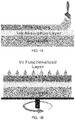
- FIG. 1A to 1C Fabrication process of the react-on-demand method.
- FIG. 1A The ink absorption layer and a thin layer of PVA polymer are brush coated onto PET substrate one by one.
- FIG. 1B Spin coating saturated ascorbic acid (Vitamin C) solution to functionalize the PVA coating.
- FIG. 1C Direct writing or printing of silver nitrate solution onto the coated layer, generating a metal-polymer highly conductive structure.
- FIG. 2A to 2C SEM images of the cross-section of
- FIG. 2A the multi-coated PET substrate before writing or printing silver nitrate ink
- FIG. 2B zoomed-in part of the squared area in FIG. 2A ;
- FIG. 2C after react-on-demand generation of silver-polymer highly conductive layer.
- FIG. 3A Optical images showing the surface of the substrate after direct-writing with 1.2 g/mL silver nitrate ink at 1 s, 5 s, 10 s, 15 s and 30 s.
- FIG. 3B Graph showing the change of sheet resistance with different silver nitrate concentration.
- the black line with square symbol corresponds to traces written with single stroke; the red line with circle symbol corresponds to traces written with double strokes.
- FIGS. 4A to 4E SEM images of the surface morphologies of single-stroke samples written with different silver nitrate concentration of:
- FIG. 4A 0.2 g/mL
- FIG. 4B 0.6 g/mL
- FIG. 4C 0.8 g/mL
- FIG. 4D 1.2 g/mL
- FIG. 4E 1.6 g/mL.
- FIGS. 4F to 4J SEM images of the surface morphologies of double-stroke samples written with different silver nitrate concentration of
- FIG. 4F 0.2 g/mL
- FIG. 4G 0.6 g/mL
- FIG. 4H 0.8 g/mL
- FIG. 4I 1.2 g/mL
- FIG. 4J 1.6 g/mL.
- FIGS. 5A to 5C X-ray photoelectron spectroscopy (XPS) spectrums of:
- FIG. 5A Ag3d
- FIG. 5B Ag MNN
- FIG. 5C O1s from traces written with 1.2 g/mL silver nitrate ink on un-functionalized coatings.
- FIGS. 5D to 5F XPS spectrums of
- FIG. 5D Ag3d
- FIG. 5E Ag MNN
- FIG. 5F O1s from traces written with 1.2 g/mL silver nitrate ink on Vc functionalized coatings.
- FIGS. 6A to 6I Optical images of a silver electrode in flat state with initial length of L0 as shown in FIG. 6A ; and bent states with length of L as shown in FIG. 6B ; and maximum bend radii with Lmin as shown in FIG. 6C .
- FIG. 6D single-stroke trace
- FIG. 6E double-stroke trace as a function of bend rate ( ⁇ L/L0%);
- FIG. 6F single-stroke trace
- FIG. 6G double-stroke trace as a function of bend cycles
- FIG. 6H single-stroke trace
- FIG. 6I double-stroke trace as a function of time.
- FIG. 7A X-ray diffraction (XRD) spectra of freshly prepared single-stroke electrode written it 1.2 g/mL silver nitrate ink;
- FIG. 7B X-ray diffraction (XRD) spectra after stored in air for 180 days.
- FIG. 8A Optical images of LEDs powered by the hand-written metal-polymer conductive traces fabricated using the proposed RoD method operating as intended in normal flat state;
- FIG. 8B when bent inward and
- FIG. 8C when bent outward.
- FIGS. 8D, 8E and 8F Optical images of high resolution functional circuits fabricated by inkjet printing using the RoD method.
- the size distribution peak of the silver nanoparticles needs to be smaller than 100 nm for low-viscosity inkjet ink.
- smaller particle size typically means worse conductivity, since a higher ratio of additives will wrap and/or bond to the surface of the nanoparticles, preventing the nanoparticles from contacting with one another when the ink dries.
- a post-sintering process can help to remove these additives using a high energy method, but the equipment needed for post-treatment is inaccessible to end-users, which consequently limits its application to handwritten electronics.
- FIGS. 1A to 1C shows the general idea and fabrication process of the RoD method.
- Pristine polyethylene terephthalate (PET) substrate was washed and brush-coated with multiple materials ( FIG. 1A )
- the first layer of coating is a commercially available water-proof ink absorption material. This kind of coating can absorb excessive solvent, which in turn reduces the drying time and helps with the ink bleeding issue.
- a second layer of polyvinyl alcohol (PVA) coating was then introduced as the reaction media for the RoD method.
- PVA polyvinyl alcohol
- the mechanism of the swelling of PVA has been well studied and has been widely used in drug delivery applications in the past decades. Briefly, small solvent molecules, like water, will diffuse into the partially cross-linked polymers in a short period of time and reside in between polymer chains. Utilizing the water-swelling property of PVA, we embedded the reducing agent into the PVA film by spin coating the saturated ascorbic acid solution, as shown in FIG. 1B . As the solvent evaporates, the ascorbic acid will crystallize and precipitate, forming small reducing crystals in between the PVA polymer chains as well as on the surface. The PVA film seals the Vc crystals when the solvent dries, and protect them from being oxidized in air. The functionalized film retains good reducing ability and function after three months of storage in a dark and dry environment.
- FIG. 2A The cross-section of the finalized coating is shown in FIG. 2A
- FIG. 2B is a zoom-in of the area marked with a box in FIG. 2A .
- the first layer of coating has a thickness of about 20 ⁇ m for efficient absorption of the solvent.
- the PVA forms a thinner layer ( ⁇ 3 ⁇ m) of coating with embedded Vc crystal.
- FIG. 2B some large Vc crystals are observable at the interface of the two layers, illustrating a successful functionalization of the coating.
- Silver nitrate was chosen as the metal precursor for its ultra-high solubility in water.
- the solubility of silver nitrate in water can reach 256 g/100 mL at room temperature (25° C.). This gives a maximum silver content loading of more than 120% (w/v), which is much higher than any commercial available silver ink.
- High solubility facilitates high loading of metal slat without increasing the amount of ink, and further contributes to the high metal content in written traces after the on-site RoD reduction.
- Aqueous silver nitrate solution was filled into a liquid ink marker with a chisel tip. This type of marker is compatible with low-viscosity ink, and the chisel tip allows users to write traces of different widths with ease, offering excellent user experience.
- FIG. 3A shows the silver reduction process using the proposed RoD method from 0 to 30 seconds after reaction at room temperature.
- the trace was written with 1.2 g/mL silver nitrate ink and the photos were taken under the same lighting conditions. For the first 5 seconds, the silver trace is barely seen. During this period, the water molecules and silver ions are absorbed by the PVA film, while at the same time, the ascorbic acid molecules embedded in the film are dissolved, forming a sectional reducing solution which reduces the silver ions immediately.
- the above process continues, and more and more silver ions are reduced; the generated silver plates/particles tend to grow larger since no capping agent is used. After 10 seconds, the trace shows a silver metallic color with a clear edge.
- the silver content loading plays a critical role in the conductivity of the final product. This is also true in the RoD method.
- the final resistance of the written traces is also affected by the amount of ink, which can be determined by the number of repeats.
- two groups of experiments were conducted; one without repeat writing (single-stroke) and the other with one repeat (double-stroke). The results are shown in FIG. 3B .
- the sheet resistance initially drops drastically with increase in concentration and starts showing good conductivity when the silver slat load reaches 0.6 g/mL. At this point, it has a sheet resistance of ⁇ 35 m ⁇ /sq, which is better than most inkjet printed circuits with silver inks. Beyond 0.8 g/mL ( ⁇ 4.70 m ⁇ /sq), the decrease in sheet resistance slows down significantly, which is attributed to the limited loading of ascorbic acid in the PVA film. The lowest sheet resistance of ⁇ 3.66 m ⁇ /sq is observed at 1.6 g/mL for the one-write group. Interestingly, the sheet resistance begins to increase slightly when the concentration of silver nitrate is higher than 1.6 g/mL.
- FIGS. 4A to 4E show the surface morphology of single-stroke traces written with 0.2 g/mL, 0.6 g/mL, 0.8 g/mL, 1.2 g/mL and 1.6 g/mL silver nitrate ink respectively.
- the reduced silver appears to be in the form of small plates with diameters ranging from 5 ⁇ m to 10 ⁇ m, with small silver particles generated through the secondary nucleation on the surface.
- the size of the silver plates is much larger than that in commercially available silver ink, which are usually on the nanometer scale.
- the relatively large silver plates contribute to the good conductivity of the silver trace.
- the trace is not conductive ( FIG.
- FIG. 4A When the concentration reaches 0.6 g/mL, more silver plates of larger size ( ⁇ 10 ⁇ m) are generated, distributing in a random orientation and overlapping with one another, as shown in FIG. 4B . It can be clearly observed that some silver plates are half on the surface, half inside the film (circles by red dot lines in FIG. 4B ), illustrating the formation of a three-dimensional silver-polymer structure. The silver plates become denser and thicker with increasing concentration of silver nitrate in the inks, but the morphology remains essentially the same, as shown in FIGS. 4C to 4E .
- FIGS. 4F to 4J show the surface morphology of double-stroke traces written with 0.2 g/mL, 0.6 g/mL, 0.8 g/mL, 1.2 g/mL and 1.6 g/mL sliver nitrate ink, respectively.
- the second stroke was repeated right after the first stroke after an interval of about 5 seconds.
- the shape of the silver plates is still visible but the morphology appears to be pressed/flattened due to the writing of the second stroke.
- the growth of the silver plates starts immediately after the first layer of ink is written onto the substrate.
- FIG. 5A to 5C show the Ag 3d, Ag MNN and O 1 s regions obtained from a single-stroke trace written with 1.6 g/mL silver nitrate ink on un-activated coating as a control group. Both the Ag 3d peak (368.63 eV, FIG. 5A ) and Ag MNN Auger peak (355.20 eV, FIG.
- FIG. 5B match the silver nitrate standard spectrum, indicating a single chemical state for silver. Combining this with the obtained Auger parameter (723.83 eV), we can confirm that only silver nitrate is presented on the surface.
- the O 1s region FIG. 5C presents a strong peak at ⁇ 533 eV, which can be attributed to the nitrate groups and PVA film.
- FIG. 5D to 5F show the same regions obtained from a single-stroke trace, written with the same concentration except on activated coating. Different from the control group, the Ag 3d peak appeared at 368.2 eV and the Ag MNN Auger peak appeared at 358 eV, which matches well with the silver metal standard spectrum.
- FIGS. 6A to 6C shows the tested sample at different bent states.
- FIG. 6A shows the initial state of the sample with electrode distance of L 0 .
- FIGS. 6D and 6E Two groups of data showing the relationship between bend rate and resistance change are presented in FIGS. 6D and 6E , corresponding to the single-stroke and double-stroke traces, respectively.
- FIGS. 6D and 6E Two groups of data showing the relationship between bend rate and resistance change are presented in FIGS. 6D and 6E , corresponding to the single-stroke and double-stroke traces, respectively.
- the increasing rate of sheet resistance is positively correlated with the ink concentration, where the 0.8 g/mL trace exhibits the smallest resistance increasing rate of ⁇ 0.13% and the 1.6 g/mL trace shows the largest increasing rate of 0.8% at the highest bend rate.
- the loss of conductivity is mainly attributed to the cracks and separation of silver plates on the PVA surface when bent outwards, and thus samples with a sparser silver layer (lower ink concentration) exhibited smaller increases in resistance.
- the bend rate is less than 40%, the resistance is almost unaffected ( ⁇ 0.1%), and even when the bend rate reaches its maximum value (75%), the resistance increment is still smaller than 1%.
- the double-stroke group as shown in FIG.
- FIGS. 6H and 6I show the resistance change of single-stroke and double-stroke traces, respectively, at different concentrations over a period of 90 days. A steady increase in resistance is observed for the single-stroke group in the first 30 days, after which the resistance remains almost unchanged in the following 60 days after formation of an oxidizing balance.
- the double-stroke traces exhibit a much better stability over time than that of the single stroke, which may be largely attributed to its dense and pressed morphology.
- the single-stroke group shows an average resistance increase of ⁇ 1.4%, while the double-stroke group shows an average resistance increase of ⁇ 0.4% over a period of three months.
- FIG. 7 presents the XRD patterns of the freshly drawn silver and silver traces stored in air for 90 days. Both samples show peaks at 38.06° and 53.41°, which can be assigned to the silver crystal plane (111) and silver oxide crystal plane (220), respectively (JCPDS Data 04-0783, 41-1104).
- the peak for Ag 2 O is slightly stronger than that of the freshly made sample, illustrating that a small amount of oxide is generated over time. Both silver oxide peaks are very weak, and the peaks for (111) silver remain almost unchanged. Thus, we concluded that the samples are relatively stable in dry air over time.
- FIGS. 8D to 8F shows some of the functional circuits fabricated by RoD based inkjet printing. Since no post-treatment is required for the RoD method, the as-printed circuits can be used immediately for electronic component mounting or deposition of other materials.
- the RoD approach can also be used in other printing system, such as aerojet printing and gravure printing, to achieve higher resolutions or higher speed of roll-to-roll (R2R) production of high performance flexible electronics.
- Poly (vinyl alcohol) (PVA) (5 g) was dissolved in DI water (90 mL) with continuous stirring for 72 hours at 85° C., yielding a clear, transparent solution.
- Xanthan gum (0.1 g) was dissolved in DI water (100 mL) at 70° C. with continuous stirring for 3 hours. After the solution cooling down to room temperature, excessive amount of ascorbic acid was added into the solution followed by gentle stirring for 1 hours. The solution was then filtered with filter paper to remove undissolved ascorbic acid, and after the filtration, we got a transparent, clear solution.
- Transparent PET film was cleaned by the mixed solution of 1:1 ethanol and acetone in ultrasonic bath for 10 mins, and was air dried at room temperature.
- InkAID ink absorption coating was applied onto the substrate by a foam brush. After the sample was completely dried in air (about 3 hours), PVA coating was applied onto the substrate as the second layer using foam brush and dried in air. Saturated ascorbic acid solution was then spin coating onto the sample using a Laurell WS-650-23B spin coating at 900 rpm. As the final step, the coated PET was dried in vacuum overnight. Silver nitrate solutions with different silver nitrate concentration were prepared by dissolving specific amount of silver nitrate in DI water. The as-prepared silver nitrate solutions were directly filled into a liquid-ink based marker pen for the following experiment.
- Silver nitrate solutions with different silver nitrate concentration were prepared by dissolving specific amount of silver nitrate in DI water.
- the as-prepared silver nitrate solutions were directly filled into a liquid-ink based marker pen for the following experiment.
- Conductive circuits were fabricated by writing the as-prepared ink onto the as-prepared substrate.
- FIGS. 8A to 8C show the handwritten circuits using the disclosed invention.
- PVA poly (vinyl alcohol) (Mw ⁇ 40 000, 98-99% hydrolyzed), ascorbic acid (99%), silver nitrate (AgNO 3 , 99%), xanthan gum ((C 35 H 49 O 29 ) n , 98%) from Sigma-Aldrich; ink absorption coating (clear) from inkAlD.
- Poly (vinyl alcohol) (PVA) (5 g) was dissolved in DI water (90 mL) with continuous stirring for 72 hours at 85° C., yielding a clear, transparent solution.
- Xanthan gum (0.1 g) was dissolved in DI water (100 mL) at 70° C. with continuous stirring for 3 hours. After the solution cooling down to room temperature, excessive amount of ascorbic acid was added into the solution followed by gentle stirring for 1 hours. The solution was then filtered with filter paper to remove undissolved ascorbic acid, and after the filtration, we got a transparent, clear solution.
- Transparent PET film was cleaned by the mixed solution of 1:1 ethanol and acetone in ultrasonic bath for 10 mins, and was air dried at room temperature.
- InkAID ink absorption coating was applied onto the substrate by a foam brush. After the sample was completely dried in air (about 3 hours), PVA coating was applied onto the substrate as the second layer using foam brush and dried in air. Saturated ascorbic acid solution was then spin coating onto the sample using a Laurell WS-650-23B spin coating at 900 rpm. As the final step, the coated PET was dried in vacuum overnight. Silver nitrate solutions with different silver nitrate concentration were prepared by dissolving specific amount of silver nitrate in DI water. The as-prepared silver nitrate solutions were directly filled into a liquid-ink based marker pen for the following experiment.
- a glycerol-water solution was prepared by mixing anhydrous glycerol and distilled water at a volume ratio of 3:2. Silver nitrate was then added, followed by mixing in a VWR mixer for 4 min to form a 1.2 g/mL silver slat solution.
- the prepared ink was degassed in a vacuum chamber at 2 psi for 2 h to remove dissolved gases and bubbles. The viscosity and surface tension of the final ink were 12.3 cp and 50.1 mN m ⁇ 1 , respectively. These values fall within the optimum operating range for the Dimatix DMP-2800 printer.
- a 0.2 ⁇ m nylon syringe filter was used to remove undesired particles from the ink.
- the ink was filled into a cartridge mounted on a 10 pL piezoelectric drop-on-demand inkjet print head.
- Printing parameters were set as following: drop space, 15 ⁇ m; meniscus vacuum, 3.5 in. of H 2 O; print head temperature, 25° C.; print head angle: 2.1°; jetting voltage ⁇ 25.1 V.
- Printing was conducted at room temperature.
- High conductive circuits were printed by inkjet printing the as-prepared silver nitrate ink onto the as-prepared substrate.
- FIGS. 8D to 8F show the inkjet printed circuits using the method disclosed in this invention.
- PVA poly (vinyl alcohol) (Mw ⁇ 40 000, 98-99% hydrolyzed), ascorbic acid (99%), anhydrous glycerol (C 3 H 5 (OH) 3 , 99%), silver nitrate (AgNO 3 , 99%), xanthan gum ((C 35 H 49 O 29 ) n , 98%) from Sigma-Aldrich; ink absorption coating (clear) from inkAlD.
- PVA poly (vinyl alcohol) (Mw ⁇ 40 000, 98-99% hydrolyzed), ascorbic acid (99%), anhydrous glycerol (C 3 H 5 (OH) 3 , 99%), silver nitrate (AgNO 3 , 99%), xanthan gum ((C 35 H 49 O 29 ) n , 98%) from Sigma-Aldrich; ink absorption coating (clear) from inkAlD.
Landscapes
- Engineering & Computer Science (AREA)
- Microelectronics & Electronic Packaging (AREA)
- Manufacturing & Machinery (AREA)
- Chemical & Material Sciences (AREA)
- Dispersion Chemistry (AREA)
- Inks, Pencil-Leads, Or Crayons (AREA)
Abstract
Description
Claims (11)
Priority Applications (2)
| Application Number | Priority Date | Filing Date | Title |
|---|---|---|---|
| US15/723,887 US10772218B2 (en) | 2017-10-03 | 2017-10-03 | React-on-demand (ROD) fabrication method for high performance printed electronics |
| CA3019721A CA3019721A1 (en) | 2017-10-03 | 2018-10-03 | React-on-demand (rod) fabrication method for high performance printed electronics |
Applications Claiming Priority (1)
| Application Number | Priority Date | Filing Date | Title |
|---|---|---|---|
| US15/723,887 US10772218B2 (en) | 2017-10-03 | 2017-10-03 | React-on-demand (ROD) fabrication method for high performance printed electronics |
Publications (2)
| Publication Number | Publication Date |
|---|---|
| US20190208646A1 US20190208646A1 (en) | 2019-07-04 |
| US10772218B2 true US10772218B2 (en) | 2020-09-08 |
Family
ID=65992256
Family Applications (1)
| Application Number | Title | Priority Date | Filing Date |
|---|---|---|---|
| US15/723,887 Expired - Fee Related US10772218B2 (en) | 2017-10-03 | 2017-10-03 | React-on-demand (ROD) fabrication method for high performance printed electronics |
Country Status (2)
| Country | Link |
|---|---|
| US (1) | US10772218B2 (en) |
| CA (1) | CA3019721A1 (en) |
Families Citing this family (3)
| Publication number | Priority date | Publication date | Assignee | Title |
|---|---|---|---|---|
| CN110054149A (en) * | 2019-04-09 | 2019-07-26 | 华东师范大学 | A kind of flexible sensor under transfer mode |
| CN113825318B (en) * | 2020-06-18 | 2023-06-23 | 天津大学 | Methods and applications for fabricating high-resolution circuits using electrofluidic inkjet printing |
| CN115442975B (en) * | 2022-09-30 | 2024-04-30 | 中纺院(浙江)技术研究院有限公司 | Preparation method of nano silver-based flexible electronic circuit |
Citations (7)
| Publication number | Priority date | Publication date | Assignee | Title |
|---|---|---|---|---|
| US3017285A (en) * | 1959-05-29 | 1962-01-16 | Horizons Inc | Method of writing on anodized aluminum |
| US20040086646A1 (en) * | 2000-11-01 | 2004-05-06 | Mariola Brandes | Method for electroless metal plating |
| US20050006339A1 (en) * | 2003-07-11 | 2005-01-13 | Peter Mardilovich | Electroless deposition methods and systems |
| US20080178761A1 (en) * | 2007-01-26 | 2008-07-31 | Konica Minolta Holdings, Inc. | Method of forming metal pattern, and metal salt mixture |
| US20090304911A1 (en) * | 2008-06-04 | 2009-12-10 | Fukui Precision Component (Shenzhen) Co., Ltd. | Method of forming circuits on circuit board |
| US9329177B2 (en) * | 2013-05-29 | 2016-05-03 | National Yang Ming University | Method for manufacturing and using a test paper and chemical composition thereof |
| US20180002814A1 (en) * | 2016-06-30 | 2018-01-04 | United Technologies Corporation | Reinforced chemical conversion coating |
-
2017
- 2017-10-03 US US15/723,887 patent/US10772218B2/en not_active Expired - Fee Related
-
2018
- 2018-10-03 CA CA3019721A patent/CA3019721A1/en not_active Abandoned
Patent Citations (7)
| Publication number | Priority date | Publication date | Assignee | Title |
|---|---|---|---|---|
| US3017285A (en) * | 1959-05-29 | 1962-01-16 | Horizons Inc | Method of writing on anodized aluminum |
| US20040086646A1 (en) * | 2000-11-01 | 2004-05-06 | Mariola Brandes | Method for electroless metal plating |
| US20050006339A1 (en) * | 2003-07-11 | 2005-01-13 | Peter Mardilovich | Electroless deposition methods and systems |
| US20080178761A1 (en) * | 2007-01-26 | 2008-07-31 | Konica Minolta Holdings, Inc. | Method of forming metal pattern, and metal salt mixture |
| US20090304911A1 (en) * | 2008-06-04 | 2009-12-10 | Fukui Precision Component (Shenzhen) Co., Ltd. | Method of forming circuits on circuit board |
| US9329177B2 (en) * | 2013-05-29 | 2016-05-03 | National Yang Ming University | Method for manufacturing and using a test paper and chemical composition thereof |
| US20180002814A1 (en) * | 2016-06-30 | 2018-01-04 | United Technologies Corporation | Reinforced chemical conversion coating |
Also Published As
| Publication number | Publication date |
|---|---|
| US20190208646A1 (en) | 2019-07-04 |
| CA3019721A1 (en) | 2019-04-03 |
Similar Documents
| Publication | Publication Date | Title |
|---|---|---|
| Jabari et al. | 2D printing of graphene: a review | |
| Nayak et al. | A review on inkjet printing of nanoparticle inks for flexible electronics | |
| Suresh et al. | Fabrication of screen-printed electrodes: opportunities and challenges | |
| Saidina et al. | Recent Development of Graphene-Based Ink and Other Conductive Material-Based Inks for Flexible Electronics: Saidina, Eawwiboonthanakit, Mariatti, Fontana, and Hérold | |
| Russo et al. | Pen‐on‐paper flexible electronics | |
| JP6373360B2 (en) | Method for producing transparent electrode film | |
| JP6280500B2 (en) | Dispersion containing carbon nanotubes and graphene platelets | |
| KR102109390B1 (en) | Ink composition for making a conductive silver structure | |
| CN105359226B (en) | Method for producing transparent electrode film for display and transparent electrode film for display | |
| US10772218B2 (en) | React-on-demand (ROD) fabrication method for high performance printed electronics | |
| KR20110028632A (en) | Core-Shell Metal Nanoparticles, Methods for Making the Same, and Ink Compositions Containing the Same | |
| US10660217B2 (en) | Methods of fast fabrication of single and multilayer circuit with highly conductive interconnections without drilling | |
| JP6659665B2 (en) | Conductive coating composite and method for producing the same | |
| CN105393314A (en) | Method for manufacturing hybrid transparent electrode and hybrid transparent electrode | |
| WO2017025697A1 (en) | Electrically conductive materials comprising graphene | |
| TW201245348A (en) | Electroconductive aqueous ink for ink-jet recording | |
| CN109563625A (en) | Laminates, metal meshes and touch panels | |
| CN104159981A (en) | Aqueous ink formulation containing metal-based nanoparticles for usage in micro contact printing | |
| You et al. | On‐demand picoliter‐level‐droplet inkjet printing for micro fabrication and functional applications | |
| US20160353578A1 (en) | Printing Method for Fabrication of Printed Electronics | |
| Rafiq et al. | Overview of printable nanoparticles through inkjet process: their application towards medical use | |
| TWI686447B (en) | Electroconductive ink for transfer printing | |
| Zhang et al. | React‐on‐Demand (RoD) Fabrication of Highly Conductive Metal–Polymer Hybrid Structure for Flexible Electronics via One‐Step Direct Writing or Printing | |
| Ismail et al. | Electrical and mechanical performance of Inkjet-printed flexible electrodes based on reduced graphene oxide/silver nanoparticles | |
| Yang | Preparation and characterization of organic silver based conductive inks for flexible electronics |
Legal Events
| Date | Code | Title | Description |
|---|---|---|---|
| FEPP | Fee payment procedure |
Free format text: ENTITY STATUS SET TO UNDISCOUNTED (ORIGINAL EVENT CODE: BIG.); ENTITY STATUS OF PATENT OWNER: SMALL ENTITY |
|
| AS | Assignment |
Owner name: THE UNIVERSITY OF WESTERN ONTARIO, CANADA Free format text: ASSIGNMENT OF ASSIGNORS INTEREST;ASSIGNORS:ZHANG, TENGYUAN;YANG, JUN;REEL/FRAME:046948/0554 Effective date: 20180613 |
|
| FEPP | Fee payment procedure |
Free format text: ENTITY STATUS SET TO SMALL (ORIGINAL EVENT CODE: SMAL); ENTITY STATUS OF PATENT OWNER: SMALL ENTITY |
|
| STPP | Information on status: patent application and granting procedure in general |
Free format text: RESPONSE TO NON-FINAL OFFICE ACTION ENTERED AND FORWARDED TO EXAMINER |
|
| STPP | Information on status: patent application and granting procedure in general |
Free format text: FINAL REJECTION MAILED |
|
| ZAAA | Notice of allowance and fees due |
Free format text: ORIGINAL CODE: NOA |
|
| ZAAB | Notice of allowance mailed |
Free format text: ORIGINAL CODE: MN/=. |
|
| STCF | Information on status: patent grant |
Free format text: PATENTED CASE |
|
| FEPP | Fee payment procedure |
Free format text: MAINTENANCE FEE REMINDER MAILED (ORIGINAL EVENT CODE: REM.); ENTITY STATUS OF PATENT OWNER: SMALL ENTITY |
|
| LAPS | Lapse for failure to pay maintenance fees |
Free format text: PATENT EXPIRED FOR FAILURE TO PAY MAINTENANCE FEES (ORIGINAL EVENT CODE: EXP.); ENTITY STATUS OF PATENT OWNER: SMALL ENTITY |
|
| STCH | Information on status: patent discontinuation |
Free format text: PATENT EXPIRED DUE TO NONPAYMENT OF MAINTENANCE FEES UNDER 37 CFR 1.362 |
|
| FP | Lapsed due to failure to pay maintenance fee |
Effective date: 20240908 |