US10770801B2 - Antenna structure including parasitic conductive plate - Google Patents
Antenna structure including parasitic conductive plate Download PDFInfo
- Publication number
- US10770801B2 US10770801B2 US16/251,763 US201916251763A US10770801B2 US 10770801 B2 US10770801 B2 US 10770801B2 US 201916251763 A US201916251763 A US 201916251763A US 10770801 B2 US10770801 B2 US 10770801B2
- Authority
- US
- United States
- Prior art keywords
- conductive plate
- disposed
- parasitic
- antenna structure
- conductive
- Prior art date
- Legal status (The legal status is an assumption and is not a legal conclusion. Google has not performed a legal analysis and makes no representation as to the accuracy of the status listed.)
- Active, expires
Links
Images


Classifications
-
- H—ELECTRICITY
- H01—ELECTRIC ELEMENTS
- H01Q—ANTENNAS, i.e. RADIO AERIALS
- H01Q19/00—Combinations of primary active antenna elements and units with secondary devices, e.g. with quasi-optical devices, for giving the antenna a desired directional characteristic
- H01Q19/005—Patch antenna using one or more coplanar parasitic elements
-
- H—ELECTRICITY
- H01—ELECTRIC ELEMENTS
- H01Q—ANTENNAS, i.e. RADIO AERIALS
- H01Q1/00—Details of, or arrangements associated with, antennas
- H01Q1/36—Structural form of radiating elements, e.g. cone, spiral, umbrella; Particular materials used therewith
- H01Q1/38—Structural form of radiating elements, e.g. cone, spiral, umbrella; Particular materials used therewith formed by a conductive layer on an insulating support
-
- H—ELECTRICITY
- H01—ELECTRIC ELEMENTS
- H01Q—ANTENNAS, i.e. RADIO AERIALS
- H01Q1/00—Details of, or arrangements associated with, antennas
- H01Q1/12—Supports; Mounting means
- H01Q1/22—Supports; Mounting means by structural association with other equipment or articles
- H01Q1/24—Supports; Mounting means by structural association with other equipment or articles with receiving set
- H01Q1/241—Supports; Mounting means by structural association with other equipment or articles with receiving set used in mobile communications, e.g. GSM
- H01Q1/242—Supports; Mounting means by structural association with other equipment or articles with receiving set used in mobile communications, e.g. GSM specially adapted for hand-held use
- H01Q1/243—Supports; Mounting means by structural association with other equipment or articles with receiving set used in mobile communications, e.g. GSM specially adapted for hand-held use with built-in antennas
-
- H—ELECTRICITY
- H01—ELECTRIC ELEMENTS
- H01Q—ANTENNAS, i.e. RADIO AERIALS
- H01Q21/00—Antenna arrays or systems
- H01Q21/06—Arrays of individually energised antenna units similarly polarised and spaced apart
- H01Q21/061—Two dimensional planar arrays
- H01Q21/065—Patch antenna array
-
- H—ELECTRICITY
- H01—ELECTRIC ELEMENTS
- H01Q—ANTENNAS, i.e. RADIO AERIALS
- H01Q9/00—Electrically-short antennas having dimensions not more than twice the operating wavelength and consisting of conductive active radiating elements
- H01Q9/04—Resonant antennas
- H01Q9/0407—Substantially flat resonant element parallel to ground plane, e.g. patch antenna
- H01Q9/0414—Substantially flat resonant element parallel to ground plane, e.g. patch antenna in a stacked or folded configuration
-
- H—ELECTRICITY
- H02—GENERATION; CONVERSION OR DISTRIBUTION OF ELECTRIC POWER
- H02J—ELECTRIC POWER NETWORKS; CIRCUIT ARRANGEMENTS OR SYSTEMS FOR SUPPLYING OR DISTRIBUTING ELECTRIC POWER; SYSTEMS FOR STORING ELECTRIC ENERGY
- H02J50/00—Circuit arrangements or systems for wireless supply or distribution of electric power
- H02J50/005—Mechanical details of housing or structure aiming to accommodate the power transfer means, e.g. mechanical integration of coils, antennas or transducers into emitting or receiving devices
-
- H—ELECTRICITY
- H02—GENERATION; CONVERSION OR DISTRIBUTION OF ELECTRIC POWER
- H02J—ELECTRIC POWER NETWORKS; CIRCUIT ARRANGEMENTS OR SYSTEMS FOR SUPPLYING OR DISTRIBUTING ELECTRIC POWER; SYSTEMS FOR STORING ELECTRIC ENERGY
- H02J50/00—Circuit arrangements or systems for wireless supply or distribution of electric power
- H02J50/10—Circuit arrangements or systems for wireless supply or distribution of electric power using inductive coupling
- H02J50/12—Circuit arrangements or systems for wireless supply or distribution of electric power using inductive coupling of the resonant type
-
- H—ELECTRICITY
- H02—GENERATION; CONVERSION OR DISTRIBUTION OF ELECTRIC POWER
- H02J—ELECTRIC POWER NETWORKS; CIRCUIT ARRANGEMENTS OR SYSTEMS FOR SUPPLYING OR DISTRIBUTING ELECTRIC POWER; SYSTEMS FOR STORING ELECTRIC ENERGY
- H02J50/00—Circuit arrangements or systems for wireless supply or distribution of electric power
- H02J50/20—Circuit arrangements or systems for wireless supply or distribution of electric power using microwaves or radio frequency waves
- H02J50/23—Circuit arrangements or systems for wireless supply or distribution of electric power using microwaves or radio frequency waves characterised by the type of transmitting antennas, e.g. directional array antennas or Yagi antennas
-
- H—ELECTRICITY
- H02—GENERATION; CONVERSION OR DISTRIBUTION OF ELECTRIC POWER
- H02J—ELECTRIC POWER NETWORKS; CIRCUIT ARRANGEMENTS OR SYSTEMS FOR SUPPLYING OR DISTRIBUTING ELECTRIC POWER; SYSTEMS FOR STORING ELECTRIC ENERGY
- H02J50/00—Circuit arrangements or systems for wireless supply or distribution of electric power
- H02J50/80—Circuit arrangements or systems for wireless supply or distribution of electric power involving the exchange of data, concerning supply or distribution of electric power, between transmitting devices and receiving devices
Definitions
- the disclosure was made by or on behalf of the below listed parties to a joint research agreement.
- the joint research agreement was in effect on or before the date the disclosure was made and the disclosure was made as a result of activities undertaken within the scope of the joint research agreement.
- the parties to the joint research agreement are 1) Samsung Electronics Co., Ltd. and 2) Korea Advanced Institute of Science and Technology.
- the disclosure relates to an antenna structure. More particularly, the disclosure relates to an antenna structure including a parasitic conductive plate.
- Electronic devices may mean devices that perform specific functions according to programs incorporated therein. Such devices include electronic schedulers, portable multimedia reproducers, mobile communication terminals, tablet PCs, image/sound devices, desktop PCs, laptop PCs, or vehicular navigation systems, as well as home appliances.
- the above-mentioned electronic devices may output, for example, information stored therein as sounds or images.
- various functions have recently been provided in a single electronic device, such as a mobile communication terminal.
- various functions such as entertainment functions (e.g., a game function), multimedia functions (e.g., a music/video reproducing function), communication and security functions for mobile banking, schedule management functions, and e-wallet functions, are integrated in a single electronic device, in addition to communication functions.
- entertainment functions e.g., a game function
- multimedia functions e.g., a music/video reproducing function
- communication and security functions for mobile banking, schedule management functions, and e-wallet functions
- next generation communication system such as a next generation (5 th -generation) communication system or a pre-next generation communication system in order to meet the growing demand for wireless data traffic, which has been an increasing trend since the commercialization of 4G (4 th -generation) communication system.
- an aspect of the disclosure is to provide a method of transmitting electric energy using an electromagnetic induction principle or a method of transmitting electric energy by radiating electromagnetic waves.
- Existing electromagnetic induction technology has a maximum chargeable distance of only 30 cm and requires a separate case or mat.
- remote wireless power transmission technology is required.
- expansion and converging low power technology, integration technology, and the like in the remote wireless power transmission technology is required.
- Wireless power transmission technology using a high-efficiency antenna may adversely affect the user's body due to the linearity of the antenna.
- Another aspect of the disclosure is to provide an antenna structure capable of improving remote wireless power transmission and reducing influence on the human body using a cavity and a parasitic conductive plate.
- an antenna structure includes at least one feeding unit, a plurality of dielectric substrates, a plurality of conductive plates disposed between the plurality of dielectric substrates and including at least one opening, and a radiator electrically connected to the feeding unit through conductive vias in the dielectric substrates or the conductive plates.
- the radiator may include a plurality of first parasitic conductive plates spaced apart from each other, and a second parasitic conductive plate disposed between the plurality of first parasitic conductive plates and spaced apart from the first parasitic conductive plates.
- an antenna structure in accordance with another aspect of the disclosure, includes at least one feeding unit, a first layer connected to the at least one feeding unit and including a first conductive plate, a second layer disposed on a front face of the first layer and including a second conductive plate, a third layer disposed on a front face of the second layer and including a third conductive plate, and a fourth layer disposed on a front face of the third layer and including a radiator electrically connected to the at least one feeding unit through conductive vias.
- the radiator may include a plurality of first parasitic conductive plates spaced apart from each other, and a second parasitic conductive plate disposed between the plurality of first parasitic conductive plates and spaced apart from the first parasitic conductive plates.
- an electronic device in accordance with another aspect of the disclosure, includes a housing, a printed circuit board disposed within the housing, a processor mounted on the printed circuit board, and an antenna structure disposed inside or outside the housing.
- the antenna structure may include a feeding unit, a dielectric substrate, an array of first parasitic conductive plates disposed on the dielectric plate to be spaced apart from each other, a second parasitic conductive plate disposed in a center of the array of the first parasitic conductive plates, first line conductors disposed to be in contact with the second parasitic plate, and second line conductors disposed perpendicular to the respective ones of the first line conductors and disposed in respective edges of the dielectric substrate.
- an antenna structure in accordance with another aspect of the disclosure, includes a parasitic conductive plate that is capable of inducing a narrow band matching characteristic of the antenna and improving single resonant frequency gain using a cavity.
- an antenna structure in accordance with another aspect of the disclosure, includes a parasitic conductive plate that is capable of ensuring high efficiency and reducing influence on the human body using a plurality of parasitic conductive plates to form a narrow beam in a predetermined direction.
- an antenna structure in accordance with another aspect of the disclosure, includes a parasitic conductive plate that is capable of providing enhanced remote wireless power transmission using a cavity and the parasitic conductive plate.
- FIG. 1 is a block diagram illustrating an electronic device in a network environment, according to an embodiment of the disclosure
- FIG. 2 is a view illustrating an example of an electronic device that supports wireless communication according to an embodiment of the disclosure
- FIG. 3 is a block diagram of an electronic device according to an embodiment of the disclosure.
- FIG. 4 is an exploded perspective view illustrating an antenna structure of a communication device according to an embodiment of the disclosure
- FIG. 5 is a cross-sectional view illustrating a stacking relationship of an antenna structure of a communication device according to an embodiment of the disclosure
- FIG. 6 is a perspective view illustrating a front face of an antenna structure of a communication device according to an embodiment of the disclosure
- FIG. 7 is a perspective view illustrating a feeding unit disposed on a rear face of an antenna structure of a communication device according to an embodiment of the disclosure
- FIG. 8 is a perspective view illustrating a first layer of an antenna structure according to an embodiment of the disclosure.
- FIG. 9 is a perspective view illustrating a second layer of an antenna structure according to an embodiment of the disclosure.
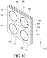
- FIG. 10 is a perspective view illustrating a third layer of an antenna structure according to an embodiment of the disclosure.
- FIG. 11 is a graph showing a return loss for each frequency band of a 2*2 array antenna structure according to an embodiment of the disclosure.
- FIG. 12 is a graph showing a directivity of a 2*2 array antenna structure according to an embodiment of the disclosure.
- FIG. 13 is a graph showing a realized gain according to a beam pattern of a 2*2 array antenna structure according to an embodiment of the disclosure.
- FIG. 1 is a block diagram illustrating an electronic device in a network environment, according to an embodiment of the disclosure.
- an electronic device 101 in a network environment 100 may communicate with an external electronic device 102 via a first network 198 (e.g., a short-range wireless communication network), or may communicate with an external electronic device 104 or a server 108 via a second network 199 (e.g., a long-range wireless communication network).
- the electronic device 101 may communicate with the external electronic device 104 via the server 108 .
- the electronic device 101 may include a processor 120 , a memory 130 , an input device 150 , a sound output device 155 , a display device 160 , an audio module 170 , a sensor module 176 , an interface 177 , a haptic module 179 , a camera module 180 , a power management module 188 , a battery 189 , a communication module 190 , a subscriber identification module 196 , or an antenna module 197 .
- at least one of these components may be eliminated from the electronic device 101 or other components may be added to the electronic device 101 .
- the sensor module 176 e.g., a fingerprint sensor, an iris sensor, or an illuminance sensor
- the display device 160 e.g., a display
- the processor 120 may control at least one other component (e.g., a hardware or software component) of the electronic device 101 , which is connected to the processor 120 , and may perform various data processing or arithmetic operations by executing, for example, software (e.g., a program 140 ). According to an embodiment, as part of data processing or operation, the processor 120 may load instructions or data received from another component (e.g., the sensor module 176 or the communication module 190 ) in a volatile memory 132 , and may process instructions or data stored in the volatile memory 132 so as to store the resulting data in a nonvolatile memory 134 .
- another component e.g., the sensor module 176 or the communication module 190
- the processor 120 may include a main processor 121 (e.g., a central processing unit or an application processor (AP)), and an auxiliary processor 123 , which operates independently from or together with the main processor 121 (e.g., a graphic processing device, an image signal processor, a sensor hub processor, or a communication processor). Additionally or alternatively, the auxiliary processor 123 may use less power than the main processor 121 , or may be set to be specific to a specified function. The auxiliary processor 123 may be implemented separately from, or as part of, the main processor 121 .
- a main processor 121 e.g., a central processing unit or an application processor (AP)
- auxiliary processor 123 which operates independently from or together with the main processor 121 (e.g., a graphic processing device, an image signal processor, a sensor hub processor, or a communication processor). Additionally or alternatively, the auxiliary processor 123 may use less power than the main processor 121 , or may be set to be specific to a specified function. The auxiliary processor
- the auxiliary processor 123 may control at least some functions or states associated with at least one of the components of the electronic device 101 (e.g., the display device 160 , the sensor module 176 , or the communication module 190 ), on behalf of the main processor 121 , for example, while the main processor 121 is in an inactive (e.g., sleep) state, or together with the main processor 121 while the main processor 121 is in an active (e.g., application execution) state.
- the auxiliary processor 123 e.g., an image signal processor or a communication processor
- the memory 130 may store various data to be used by at least one component of the electronic device 101 (e.g., the processor 120 or the sensor module 176 ).
- the data may include, for example, input data or output data for software (e.g., the program 140 ) and instructions associated therewith.
- the memory 130 may include, for example, the volatile memory 132 or the nonvolatile memory 134 .
- the program 140 may be stored in the memory 130 as software, and may include, for example, an operating system 142 , middleware 144 , or an application 146 .
- the input device 150 may receive instructions or data for use in a component (e.g., the processor 120 ) of the electronic device 101 from the outside (e.g., the user) of the electronic device 101 .
- the input device 150 may include, for example, a microphone, a mouse, or a keyboard.
- the sound output device 155 may output sound signals to the outside of the electronic device 101 .
- the sound output device 155 may include, for example, a speaker or a receiver.
- the speaker may be used for general purposes such as multimedia playback or record playback, and the receiver may be used for receiving incoming calls. According to an embodiment, the receiver may be implemented separately from, or as part of, the speaker.
- the display device 160 may visually provide information to the outside (e.g., the user) of the electronic device 101 .
- the display device 160 may include, for example, a display, a hologram device, or a projector and a control circuit configured to control the device.
- the display device 160 may include a touch circuit configured to sense a touch, or a sensor circuit (e.g., a pressure sensor) configured to measure the strength of a force generated by the touch.
- the audio module 170 may convert sound into an electrical signal, or vice versa. According to an embodiment, the audio module 170 may acquire sound through the input device 150 or may output sound through the sound output device 155 or an external electronic device (e.g., the external electronic device 102 (e.g., a speaker or headphone)) directly or wirelessly connected with the electronic device 101 .
- an external electronic device e.g., the external electronic device 102 (e.g., a speaker or headphone) directly or wirelessly connected with the electronic device 101 .
- the sensor module 176 may sense an operating state (e.g., power or temperature) of the electronic device 101 or an external environmental state (e.g., the user state), and may generate an electrical signal or a data value corresponding to the sensed state.
- the sensor module 176 may include, for example, a gesture sensor, a gyro sensor, an atmospheric pressure sensor, a magnetic sensor, an acceleration sensor, a grip sensor, a proximity sensor, a color sensor, an IR (infrared) sensor, a biometric sensor, a temperature sensor, a humidity sensor, or an illuminance sensor.
- the interface 177 may support one or more designated protocols that may be used by the electronic device 101 so as to be directly or wirelessly connected to an external electronic device (e.g., the external electronic device 102 ).
- the interface 177 may include, for example, a high definition multimedia interface (HDMI), a universal serial bus (USB) interface, a secure digital (SD) card interface, or an audio interface.
- HDMI high definition multimedia interface
- USB universal serial bus
- SD secure digital
- a connection terminal 178 may include a connector through which the electronic device 101 may be physically connected to an external electronic device (e.g., the external electronic device 102 ).
- the connection terminal 178 may include, for example, an HDMI connector, a USB connector, an SD card connector, or an audio connector (e.g., a headphone connector).
- the haptic module 179 may convert an electrical signal into a mechanical stimulus (e.g., vibration or motion) or an electrical stimulus that may be perceived by the user through a tactile or kinesthetic sense.
- the haptic module 179 may include, for example, a motor, a piezoelectric element, or an electrical stimulation device.
- the camera module 180 is a device that is capable of capturing, for example, a still image and a video image. According to an embodiment, the camera module 180 may include one or more lenses, image sensors, image signal processors, or flashes.
- the power management module 188 may manage the power to be supplied to the electronic device 101 .
- the power management module 388 may be implemented as at least a portion of, for example, a power management integrated circuit (PMIC).
- PMIC power management integrated circuit
- the battery 189 is capable of supplying power to at least one component of the electronic device 101 .
- the battery 189 may include, for example, a non-rechargeable primary battery, a rechargeable secondary battery, or a fuel cell.
- the communication module 190 may establish a direct (e.g., wired) communication channel or a wireless communication channel between the electronic device 101 and an external electronic device (e.g., the external electronic device 102 , the external electronic device 104 , or the server 108 ), and may support communication via the established communication channel.
- the communication module 190 may include one or more communication processors, which are operated independently from the processor 120 (e.g., an AP) and support direct (e.g., wired) communication or wireless communication.
- the communication module 190 may include a wireless communication module 192 (e.g., a cellular communication module, a short-range wireless communication module, or a global navigation satellite system (GNSS) communication module) or a wired communication module 194 (e.g., a local area network (LAN) communication module or a power line communication module).
- a wireless communication module 192 e.g., a cellular communication module, a short-range wireless communication module, or a global navigation satellite system (GNSS) communication module
- GNSS global navigation satellite system
- wired communication module 194 e.g., a local area network (LAN) communication module or a power line communication module.
- a corresponding one of these communication modules may communicate with an external electronic device via the first network 198 (e.g., a short-range communication network such as Bluetooth, Wi-Fi direct, or Infrared Data Association (IrDA) or the second network 199 (e.g., a cellular network, the Internet, or a computer network (e.g., a telecommunication network such as a LAN or wide area network (WAN)).
- first network 198 e.g., a short-range communication network such as Bluetooth, Wi-Fi direct, or Infrared Data Association (IrDA)
- the second network 199 e.g., a cellular network, the Internet, or a computer network (e.g., a telecommunication network such as a LAN or wide area network (WAN)
- These various types of communication modules may be integrated into one component (e.g., a single chip) or may be implemented as a plurality of components (e.g., a plurality of chips) that are separate from each other
- the wireless communication module 192 may identify or authenticate the electronic device 101 in a communication network such as the first network 198 or the second network 199 using subscriber information (e.g., international mobile subscriber identity (IMSI)) stored in the subscriber identification module 196 .
- subscriber information e.g., international mobile subscriber identity (IMSI)
- the antenna module 197 may transmit/receive signals or power to/from the outside (e.g., an external electronic device).
- the antenna module 197 may include one or more antennas, from which at least one antenna suitable for a communication scheme used in a communication network, such as the first network 198 or the second network 199 , may be selected by, for example, the communication module 190 .
- the signals or power may be transmitted or received between the communication module 190 and the external electronic device via the selected at least one antenna.
- At least some components may be connected to each other via a communication scheme (e.g., a bus, a general-purpose input and output (GPIO), a serial peripheral interface (SPI), or a mobile industry processor interface (MIPI)), and may exchange signals (e.g., commands or data) therebetween.
- a communication scheme e.g., a bus, a general-purpose input and output (GPIO), a serial peripheral interface (SPI), or a mobile industry processor interface (MIPI)
- signals e.g., commands or data
- the commands or data may be transmitted or received between the electronic device 101 and the external electronic device 104 via the server 108 connected to the second network 199 .
- Each of the external electronic devices 102 and 104 may be of a type, which is the same as or different from the electronic device 101 .
- all or some of the operations executed on the electronic device 101 may be executed on one or more of the external electronic devices 102 and 104 and the server 108 .
- the electronic device 101 may request that one or more external electronic devices perform the function or at least part of the service, in place of or in addition to performing the function or service by itself.
- the one or more external electronic devices that receives the request may execute at least a portion of the requested function or service, or an additional function or service associated with the request, and may deliver the result of the execution to the electronic device 101 .
- the electronic device 101 may process the result as it is or additionally so as to provide at least a portion of the response to the request.
- cloud computing technology distributed computing technology, or client-server computing technology may be used.
- An electronic device may be various types of devices.
- the electronic device may, for example, include at least one of a portable communication device (e.g., smartphone) a computer device, a portable multimedia device, a portable medical device, a camera, a wearable device, and a home appliance.
- a portable communication device e.g., smartphone
- first and second may simply be used to distinguish corresponding components from the other components, and the components are not limited in other respects (e.g., importance or order).
- first e.g., first
- second another component
- a term “functionally” or “communicatively” it means that the certain component can be connected directly (e.g., by wire), wirelessly, or via a third component to the another component.
- module may include a unit consisting of hardware, software, or firmware, and may, for example, be used interchangeably with the term “logic”, “logical block”, “component”, “circuit”, or the like.
- the “module” may be an integrated component, or a minimum unit for performing one or more functions or a part thereof.
- the module may be implemented in the form of an application-specific integrated circuit (ASIC).
- ASIC application-specific integrated circuit
- Various embodiments disclosed herein may be implemented by software (e.g., the program 140 ) including one or more instructions stored in a storage medium (e.g., an internal memory 136 or an external memory 138 ) readable by a machine (e.g., the electronic device 101 ).
- a processor e.g., the processor 120
- a device e.g., the electronic device 101
- the one or more instructions may include code generated by a compiler or code capable of being executed by an interpreter.
- the machine-readable storage medium may be provided in the form of a non-transitory storage medium.
- non-transient merely means that the storage medium is a tangible device and does not contain a signal (e.g., electromagnetic waves), and this term is not intended to distinguish a case where data is permanently stored on the storage medium and a case where data is temporarily stored.
- the method according to various embodiments disclosed herein may be included and provided in a computer program product.
- the computer program product may be traded as a product between a seller and a buyer.
- the computer program product may be distributed in the form of a machine-readable storage medium (e.g., compact disc read only memory (CD-ROM)), or may be distributed online via an application store (e.g., Play Store) or directly between two user devices (e.g., smartphones). If distributed online, at least part of the computer program product may be temporarily generated or at least temporarily stored in the machine-readable storage medium, such as memory of the manufacturer's server, a server of the application store, or a relay server.
- CD-ROM compact disc read only memory
- each (e.g., a module or a program) of the above-described components may include one or more entities.
- one or more of the components or operations described above may be omitted, or one or more other components or operations may be added.
- a plurality of components e.g., modules or programs
- the integrated component may perform one or more functions of each of the plurality of components may be performed in the same or similar manner as being performed by the corresponding one of the plurality of components prior to the integration.
- operations performed by a module, a program, or other components may be performed sequentially, in parallel, repetitively, or heuristically, one or more of the operations may be performed in a different order or omitted, or one or more other operations may be added thereto.
- an electronic device according to various embodiments will be described with reference to the accompanying drawings.
- the term “user” may refer to a person who uses an electronic device or a device that uses an electronic device (e.g., an artificial intelligence electronic device).
- FIG. 2 is a view illustrating an example of an electronic device that supports wireless communication according to an embodiment of the disclosure.
- the electronic device 101 includes a housing 210 , a processor 240 , a communication module 250 (e.g., the communication module 190 in FIG. 1 ), a first communication device 221 , a second communication device 222 , a third communication device 223 , a fourth communication device 224 , a first conductive line 231 , a second conductive line 232 , a third conductive line 233 , or a fourth conductive line 234 .
- a communication module 250 e.g., the communication module 190 in FIG. 1
- a first communication device 221 e.g., the communication module 190 in FIG. 1
- a second communication device 222 e.g., the communication module 190 in FIG. 1
- a third communication device 223 e.g., the third communication device 223
- a fourth communication device 224 e.g., the communication module 190 in FIG. 1
- a first communication device 221 e.g., the communication module 190 in
- the housing 210 is capable of protecting the other components of the electronic device 101 .
- the housing 210 may include, for example, a front plate, a rear plate facing away from the front plate, and a side member (or a metal frame) attached to or integrally formed with the rear plate and surrounding a space between the front plate and the rear plate.
- the electronic device 101 may include at least one communication device.
- the electronic device 101 may include at least one of the first communication device 221 , the second communication device 222 , the third communication device 223 , and the fourth communication device 224 .
- the first communication device 221 , the second communication device 222 , the third communication device 223 , or the fourth communication device 224 may be located within the housing 210 .
- the first communication device 221 when viewed from above the rear plate of the electronic device, the first communication device 221 may be located at the upper-left end of the electronic device 101 , the second communication device 222 may be located at the upper-right end of the electronic device 101 , the third communication device 223 may be disposed at the lower-left end of the electronic device 101 , and the fourth communication device 224 may be disposed at the lower-right end of the electronic device 101 .
- the processor 240 may include one or more of a central processing unit, an AP, a graphic processing unit (GPU), a camera image signal processor, or a baseband processor (or a communication processor (CP)).
- the processor 240 may be implemented as a system on chip (SoC) or a system in package (SiP).
- SoC system on chip
- SiP system in package
- the communication module 250 may be electrically connected to at least one communication device using at least one conductive line.
- the communication module 250 be electrically connected to the first communication device 221 , the second communication device 222 , the third communication device 223 , or the fourth communication device 224 using the first conductive line 231 , the second conductive line 232 , the third conductive line 233 , or the fourth conductive line 234 .
- the communication module 250 may include, for example, a baseband processor, or at least one communication circuit (e.g., an IFIC, or a radio frequency integrated circuit (RFIC)).
- the communication module 250 may include, for example, a baseband processor (e.g., an AP) separate from the processor 240 .
- the first conductive line 231 , the second conductive line 232 , the third conductive line 233 or the fourth conductive line 234 may include, for example, a coaxial cable or an FPCB.
- the communication module 250 may include a first baseband processor (BP) (not illustrated) or a second BP (not illustrated).
- the electronic device 101 may further include one or more interfaces for supporting chip-to-chip communication between the first BP (or the second BP) and the processor 240 .
- the processor 240 and the first BP or the second BP may transmit and receive data using an inter-chip interface (inter-process communication channel).
- the first BP or the second BP may provide an interface for performing communication with other entities.
- the first BP may support, for example, wireless communication for a first network (not illustrated).
- the second BP may support, for example, wireless communication for a second network (not illustrated).
- the first BP or the second BP may form one module with the processor 240 .
- the first BP or the second BP may be integrally formed with the processor 240 .
- the first BP or the second BP may be disposed in one chip, or may be formed in the form of an independent chip.
- the processor 240 and at least one BP e.g., the first BP
- SoC chip SoC chip
- the other BP e.g., the second BP
- a first network (not illustrated) or a second network (not illustrated) may correspond to the second network 199 of FIG. 1 .
- each of the first network (not illustrated) and the second network (not illustrated) may include a 4G (4 th generation) network and a 5G (5 th generation) network.
- the 4G network may support, for example, a LTE protocol defined in 3GPP.
- the 5G network may support, for example, a NR protocol defined in 3GPP.
- FIG. 3 is a block diagram of an electronic device according to an embodiment of the disclosure.
- a communication device 300 may include a communication circuit 330 (e.g., an RFIC), a printed circuit board (PCB) 350 , a first antenna array 340 , or a second antenna array 345 .
- a communication circuit 330 e.g., an RFIC
- PCB printed circuit board
- the communication circuit 330 , the first antenna array 340 , or the second antenna array 345 may be disposed on the PCB 350 .
- the first antenna array 340 or the second antenna array 345 may be disposed on a first face of the PCB 350 and the communication circuit 330 may be disposed on the second face of the PCB 350 .
- the PCB 350 may include a connector (e.g., a coaxial cable connector or a Board to Board (B-to-B) connector) to be electrically connected to another PCB (e.g., a PCB on which the communication module 250 of FIG. 2 is disposed) using a transmission line (e.g., the first conductive line 231 in FIG. 2 or a coaxial cable).
- a connector e.g., a coaxial cable connector or a Board to Board (B-to-B) connector
- the PCB 350 is coaxially connected to a PCB on which the communication module 250 is disposed using, for example, a coaxial cable connector, and the coaxial cable may be used for delivering a transmission and reception IF signal or RF signal. As another example, power or other control signals may be communicated through the B-to-B connector.
- the first antenna array 340 or the second antenna array 345 may include a plurality of antennas.
- the antennas may include a patch antenna, a loop antenna, or a dipole antenna.
- the plurality of antennas included in the first antenna array 340 may be patch antennas to form a beam toward the rear plate of the electronic device 200 .
- the plurality of antennas included in the second antenna array 345 may be a dipole antenna or a loop antenna in order to form a beam toward the side member of the electronic device 200 .
- the communications circuit 330 may support at least some of the bands that are 6 GHZ or less. As another example, the communication circuit 330 may support at least a part of a band from 6 GHz to 300 GHz (e.g., from 24 GHz to 30 GHz or from 37 GHz to 40 GHz). According to an embodiment, the communication circuit 330 may upconvert or downconvert the frequency. For example, the communication circuit 330 included in the communication device 300 (e.g., the first communication device 221 in FIG. 2 ) may upconvert an IF signal received from a communication module (e.g., the communication module 250 in FIG. 2 ) via a conductive line (e.g., the first conductive line 231 in FIG.
- a communication module e.g., the communication module 250 in FIG. 2
- a conductive line e.g., the first conductive line 231 in FIG.
- the communication circuit 330 included in the communication device 300 may downconvert an RF signal (e.g., a millimeter wave signal) received via the first antenna array 340 or the second antenna array 345 into an IF signal, and may transmit the IF signal to the communication module using a conductive line.
- an RF signal e.g., a millimeter wave signal
- FIG. 4 is an exploded perspective view illustrating an antenna structure of a communication device according to an embodiment of the disclosure.
- FIG. 5 is a cross-sectional view illustrating a stacking relationship of an antenna structure of a communication device according to an embodiment of the disclosure.
- X in an orthogonal coordinate system of three axes may indicate the longitudinal direction of an antenna structure 500
- Y may indicate the width direction of the antenna structure 500
- Z may indicate the thickness direction of the antenna structure 500 .
- Z may indicate a first direction (+Z) or a second direction ( ⁇ Z).
- an electronic device may include one or more communication devices (e.g., the first, second, third, and fourth communication devices 221 , 222 , 223 , and 224 of FIG. 2 and the communication device 300 in FIG. 3 ).
- the communication device may include a communication circuit (e.g., the communication circuit 300 in FIG. 3 ) and an antenna structure (e.g., the first and second antenna arrays 340 and 345 in FIG. 3 ).
- the antenna structure 500 may have a plurality of stacked and arranged layers (e.g., a first layer 510 , a second layer 520 , a third layer 530 , and a fourth layer 540 ).
- the plurality of layers may include a plurality of dielectric substrates (e.g., a first dielectric substrate 510 a, a second dielectric substrate 520 a, a third dielectric substrate 530 a, and a fourth dielectric substrate 540 a ), and conductive plates (e.g., a first conductive plate 510 b, a second conductive plate 520 b, and a third conductive plate 530 b ), each having a grid structure composed of a combination of openings (e.g., slots or cavities) and/or conductive vias and disposed between the plurality of dielectric substrates.
- the antenna structure 500 may include feeding units 550 and a radiator 540 b connected to some of the first, second, and third conductive plates 510 b, 520 b, and 530 b.
- the antenna structure 500 may include the second layer 520 , the third layer 530 , and the fourth layer 540 , which are oriented in the first direction (+Z) with respect to the first layer 510 to which the feeding units 550 are connected.
- Each of the first layer 510 , the second layer 520 , the third layer 530 , and the fourth layer 540 may include at least one dielectric substrate and at least one conductive plate.
- the stacked structure of the antenna structure 500 is not limited to four layers, and may be provided with three or less layers or four or more layers for the efficiency of the antenna structure. For example, as the number of layers of the antenna structure increases, a resonance frequency bandwidth may increase.
- the antenna structure 500 may have a plurality of regions which are formed in the same structure and arranged regularly or periodically.
- the antenna structure 500 may be configured such that the first, second, and third conductive plates 510 b, 520 b, and 530 b or the first, second, third, and fourth dielectric substrates 510 a, 520 a, 530 a, and 540 a arranged in the horizontal direction (X-axis and Y-axis directions) may form a 2*2 arrangement, and each of the layers may be provided in an array having the same structure.
- Each of the layers may be constituted by a total of four regions (e.g., a first region S 1 , a second region S 2 , a third region S 3 , and a fourth region S 4 ), and the structures of the respective regions may be equal to each other.
- a first region S 1 a second region S 2 , a third region S 3 , and a fourth region S 4
- the structures of the respective regions may be equal to each other.
- the structure provided in the first region S 1 will be described, and the description will be applied to the structures of the second, third, and fourth regions S 2 , S 3 , and S 4 .
- the first layer 510 of the antenna structure 500 may include a base layer 510 c on which the feeding units 550 are disposed, the first conductive plate 510 b, and the first dielectric substrate 510 a.
- the first dielectric substrate 510 a and the first conductive plate 510 b may be stacked and arranged in the first direction (+Z).
- the feeding units 550 may be electrically connected to the radiator 540 b provided on the front face of the antenna structure 500 to apply an RF signal current so as to supply an RF signal to the radiator 540 b or to receive another RF signal received through the radiator 540 b.
- the radiator 540 b may be implemented in various forms such as a rod, a meander line, a patch, and a microstip.
- the radiator 540 b may be electrically connected to the feeding units 550 to transmit and receive an RF signal in at least one frequency band.
- the first dielectric substrate 510 a may be disposed on the front face of the base layer 510 c.
- the first dielectric substrate 510 a may have the same size (e.g., area) as the base layer 510 c, and may be stacked thereon.
- a plurality of first conductive vias 511 may be arranged in a region of the first dielectric substrate 510 a.
- the plurality of first conductive vias 511 may pass through the first dielectric substrate 510 a, may extend to the first conductive plate 510 b in the first direction (+Z), and may extend to the base layer 510 c in the second direction ( ⁇ Z).
- the plurality of first conductive vias 511 may extend to the second conductive plate 520 b in the first direction (+Z) so as to provide an electrical connection from the feeding units 550 to the radiator 540 b.
- an array of the plurality of first conductive vias 511 may be arranged in a closed line shape so as to provide a narrow beam of radio waves directed in a first direction (+Z) as a waveguide.
- the first conductive plate 510 b may be disposed on the front face of the first dielectric substrate 510 a.
- the first conductive plate 510 b may have the same size (e.g., area) as the first dielectric substrate 510 a and/or the base layer 510 c, and may be stacked thereon.
- the plurality of first conductive vias 511 may be arranged in a region of the first conductive plate 510 b.
- the plurality of first conductive vias 511 are formed through the first conductive plate 510 b, and a first coupling slot 513 may be disposed inside the array of the plurality of first conductive vias 511 .
- the first coupling slot 513 is formed through the first conductive plate 510 b, and may be disposed in the central region of the first conductive plate 510 b.
- the second layer 520 of the antenna structure 500 may include the second conductive plate 520 b and the second dielectric substrate 520 a.
- the second dielectric substrate 520 a and the second conductive plate 520 b may be stacked and arranged in the first direction (+Z).
- the second dielectric substrate 520 a may be disposed on the front face of the first conductive plate 510 b of the first layer 510 .
- the second dielectric substrate 520 a may have the same size (e.g., area) as the first conductive plate 510 b of the first layer 510 , and may be stacked thereon.
- a plurality of second conductive vias 521 may be arranged in a region of the second dielectric substrate 520 a.
- the plurality of second conductive vias 521 may pass through the second dielectric substrate 520 a, and may extend to the second conductive plate 520 b in the first direction (+Z).
- the plurality of second conductive vias 521 may be connected to the first layer 510 , and may extend to the third conductive plate 530 b in the first direction (+Z) so as to provide an electrical connection from the feeding units 550 to the radiator 540 b.
- an array of the plurality of second conductive vias 521 may be arranged in a closed line shape so as to provide a narrow beam of radio waves directed in a first direction (+Z) as a waveguide.
- the second conductive plate 520 b may be disposed on the front face of the second dielectric substrate 520 a.
- the second conductive plate 520 b may have the same size (e.g., area) as the second dielectric substrate 520 a, and may be stacked thereon.
- the plurality of second conductive vias 521 may be arranged in a region of the second conductive plate 520 b.
- the plurality of second conductive vias 521 are formed through the second conductive plate 520 b, and a second coupling slot 523 may be disposed inside the array of the plurality of second conductive vias 521 .
- the second coupling slot 523 is formed through the second conductive plate 520 b, and may be disposed in the central region of the second conductive plate 520 b.
- the third layer 530 of the antenna structure 500 may include the third conductive plate 530 b and the third dielectric substrate 530 a.
- the third dielectric substrate 530 a and the third conductive plate 530 b may be stacked and arranged in the first direction (+Z).
- the third dielectric substrate 530 a may be disposed on the front face of the second conductive plate 520 b of the second layer 520 .
- the third dielectric substrate 530 a may have the same size (e.g., area) as the second conductive plate 520 b of the second layer 520 , and may be stacked thereon.
- a plurality of third conductive vias 531 may be arranged in a region of the third dielectric substrate 530 a.
- the plurality of third conductive vias 531 may pass through the third dielectric substrate 530 a, and may extend to the third conductive plate 530 b in the first direction (+Z).
- the plurality of third conductive vias 531 may extend so as to provide an electrical connection from the feeding units 550 to the radiator 540 b.
- the third conductive plate 530 b may be disposed on the front face of the third dielectric substrate 530 a.
- the third conductive plate 530 b may have the same size (e.g., area) as the third dielectric substrate 530 a, and may be stacked thereon.
- the plurality of third conductive vias 531 may be arranged in a region of the third conductive plate 530 b.
- the plurality of third conductive vias 531 are formed through the third conductive plate 530 b, and at least one cavity 533 may be disposed inside the array of the plurality of third conductive vias 531 .
- the at least one cavity 533 may be provided in a circular shape, may be formed through the third conductive plate 530 b, and may be disposed in the central region of the third conductive plate 530 b.
- the fourth layer 540 may be disposed on the front face of the third layer 530 .
- the fourth layer 540 may include the fourth dielectric substrate 540 a and the radiator 540 b.
- the fourth dielectric substrate 540 a may be disposed on the front face of the third conductive plate 530 b.
- the fourth dielectric substrate 540 a may have the same size (e.g., area) as the third conductive plate 530 b, and may be stacked thereon.
- the fourth dielectric substrate 540 a may be disposed on the front face of the third conductive plate 530 b of the third layer 530 .
- the fourth dielectric substrate 540 a may have the same size (e.g., area) as the third conductive plate 530 b of the third layer 530 , and may be stacked thereon.
- a first parasitic conductive plate(s) 541 and a second parasitic conductive plate 543 may be disposed on the front face of the fourth dielectric substrate 540 a.
- the front surface of the fourth dielectric substrate 540 a may include a first line conductor(s) 545 and a second line conductor(s) 547 .
- the first conductive plate 510 b, the second conductive plate 520 b, the first line conductor(s) 545 , and the second line conductor(s) 547 may be provided as a radiator of the antenna structure 500 .
- FIG. 6 is a perspective view illustrating the front face of the antenna structure 500 of a communication device according to an embodiment of the disclosure.
- the antenna structure 500 may have a plurality of stacked and arranged layers (e.g., the first layer 510 , the second layer 520 , the third layer 530 , and the fourth layer 540 ).
- the plurality of layers may include a plurality of dielectric substrates (e.g., the first dielectric substrate 510 a, the second dielectric substrate 520 a, the third dielectric substrate 530 a, and the fourth dielectric substrate 540 a ), and conductive plates (e.g., the first conductive plate 510 b, the second conductive plate 520 b, and the third conductive plate 530 b ) disposed between the plurality of dielectric substrates.
- dielectric substrates e.g., the first dielectric substrate 510 a, the second dielectric substrate 520 a, the third dielectric substrate 530 a, and the fourth dielectric substrate 540 a
- conductive plates e.g., the first conductive plate 510 b, the second conductive plate 520 b
- the fourth layer 540 of the antenna structure may include the fourth dielectric substrate 540 a and one or more parasitic conductive plates (e.g., first and second parasitic conductive plates 541 and 543 ) and the first and second line conductors 545 and 547 arranged on the fourth dielectric substrate 540 a.
- parasitic conductive plates e.g., first and second parasitic conductive plates 541 and 543
- first and second line conductors 545 and 547 arranged on the fourth dielectric substrate 540 a.
- quadrants may be formed with respect to the center O thereof, and respective quadrants may be divided into the first, the second, the third, and the fourth regions S 1 , S 2 , S 3 , and S 4 .
- the fourth dielectric substrate 540 a may include the second region S 2 , the third region S 3 , and the fourth region S 4 in a counterclockwise direction from the first region S 1 disposed in the upper right end region, and the respective regions may be arranged to be in contact with each other.
- the first, the second, the third, and the fourth regions S 1 , S 2 , S 3 , and S 4 may have the same area.
- the fourth dielectric substrate 540 a may be utilized as a ground panel of the antenna structure 500 .
- the thickness of the fourth dielectric substrate 540 a may be greater than the thickness of the one or more parasitic conductive plate and the thickness of the first and second line conductors 545 and 547 arranged on the fourth dielectric substrate 540 a.
- the fourth dielectric substrate 540 a may have a thickness of about 0.408 mm to 0.608 mm.
- the fourth dielectric substrate 540 a may have a thickness of about 0.508 mm.
- the front face of the fourth dielectric substrate 540 a may include the first parasitic conductive plate(s) 541 in a tetragonal shape and the second parasitic conductive plate 543 disposed to be spaced apart from the first parasitic conductive plate(s) 541 .
- the front face of the fourth dielectric substrate 540 a may include the first line conductor(s) 545 disposed adjacent to the second parasitic conductive plate 543 and the second line conductor(s) 547 disposed on the edge regions of the fourth dielectric substrate 540 a.
- a plurality of first parasitic conductive plates may be disposed on a face directed in the first direction (+Z) of the fourth dielectric substrate 540 a.
- first parasitic conductive plate(s) 541 may be disposed in each of the first, the second, the third, and the fourth regions S 1 , S 2 , S 3 , and S 4 formed by the fourth dielectric substrate 540 a.
- the first parasitic conductive plate(s) 541 may serve as a radiator of the antenna structure 500 .
- the first parasitic conductive plate(s) 541 may be provided in a patch type.
- the first parasitic conductive plate(s) 541 may be electrically connected to the feeding units 550 so as to transmit and receive an RF signal in at least one frequency band.
- the first parasitic conductive plate(s) 541 is not limited to the patch type, and may be implemented in various types such as a rod, a meander line, and a microstrip in order to enhance the usability of the antenna structure.
- a (1-1) th parasitic conductive plate 541 a may be disposed in the center of the first region S 1 .
- the (1-1) th parasitic conductive plate 541 a may be formed in a rectangular shape, and a resonance frequency may be determined by the length of the (1-1) th parasitic conductive plate 541 a.
- a (1-2) th parasitic conductive plate 541 b may be disposed in the center of the second region S 2 .
- the (1-2) th parasitic conductive plate 541 b may be formed in a rectangular shape, and a resonance frequency may be determined by the length of the (1-2) th parasitic conductive plate 541 b.
- a (1-3) th parasitic conductive plate 541 c may be disposed in the center of the third region S 3 .
- the (1-3) th parasitic conductive plate 541 c may be formed in a rectangular shape, and a resonance frequency may be determined by the length of the (1-3) th parasitic conductive plate 541 c.
- a (1-4) th parasitic conductive plate 541 d may be disposed in the center of the fourth region S 4 .
- the (1-4) th parasitic conductive plate 541 d may be formed in a rectangular shape, and a resonance frequency may be determined by the length of the (1-4) th parasitic conductive plate 541 d.
- an array of first parasitic conductive plates may be formed on one face of the fourth dielectric substrate 540 a, and there may be various shapes thereof.
- patch type first parasitic conductive plates 541 may be arranged on one face of the fourth dielectric substrate 540 a so as to form an N*M antenna array (N and M are natural numbers).
- an array of first parasitic conductive plates may be disposed in a region adjacent to a side portion of an electronic device (e.g., the electronic device 101 in FIGS. 1 and 2 ).
- the array of first parasitic conductive plates may be positioned such that the first parasitic conductive plates 541 are spaced apart from each other in order to reduce the coupling effect of the antenna.
- the circular polarization characteristic of the antenna may be determined by the size and rotation angle of the first parasitic conductive plate(s) 541 .
- the resonance frequency propagated into the air may be adjusted to about 5.8 GHz by adjusting the length and width of the patch formed by the first parasitic conductive plate(s) 541 , and the resonance frequency may be adjusted to have a circular polarization characteristic by rotating the first parasitic conductive plate(s) 541 .
- one edge of the (1-1) th parasitic conductive plate 541 a disposed on the first region S 1 may be located in the state of being rotated or tilted by a predetermined angle ⁇ so as not to be parallel to one edge of the fourth dielectric substrate 540 a so as not to be parallel to one edge of the first and second end portions.
- one edge 5411 a of the (1-1) th parasitic conductive plate 541 a may be located in the state of being rotated by a predetermined angle ⁇ with respect a virtual line 5401 e parallel to a first edge 5401 a of the fourth dielectric substrate 540 a.
- the (1-1) th parasitic conductive plate 541 a may set the circular polarization characteristic of the corresponding antenna differently depending on the rotated angle ⁇ .
- the (1-2) th parasitic conductive plate 541 b, the (1-3) th parasitic conductive plate 541 c, and the (1-4) th parasitic conductive plate 541 d may be located to be may be rotated or tilted so as to have an incline corresponding to that of the (1-1) th parasitic conductive plate 541 a.
- the thickness of the first parasitic conductive plate(s) 541 may be smaller than the thickness of the fourth dielectric substrate 540 a.
- the first parasitic conductive plate(s) 541 may have a thickness of about 0.050 mm to 0.100 mm.
- the first parasitic conductive plate(s) 541 may have a thickness of about 0.075 mm.
- the second parasitic conductive plate 543 may be disposed on a face directed in the first direction (+Z) of the fourth dielectric substrate 540 a.
- the second parasitic conductive plate 543 may be disposed between the plurality of first parasitic conductive plate(s) 541 .
- the second parasitic conductive plate 543 may be disposed so as to be spaced apart from the plurality of first parasitic conductive plate(s) 541 .
- the second parasitic conductive plate 543 may be located at a position surrounded by the positions where the (1-1) th parasitic conductive plate 541 a, the (1-2) th parasitic conductive plate 541 b, the (1-3) th parasitic conductive plate 541 c, and the (1-4) th parasitic conductive plate 541 d are arranged.
- the second parasitic conductive plate 543 may be disposed in the central portion O of the fourth dielectric substrate 540 a so as to be exposed in the first direction (+Z).
- the second parasitic conductive plate 543 may be disposed so as to at least partially overlap each of the first, the second, the third, and the fourth regions S 1 , S 2 , S 3 , and S 4 formed in the fourth dielectric substrate 540 a.
- the second parasitic conductive plate 543 may serve as a radiator of the antenna structure 500 .
- the second parasitic conductive plate 543 may be provided in a patch type.
- the second parasitic conductive plate 543 may be electrically connected to the feeding units 550 so as to transmit and receive an RF signal in at least one frequency band.
- the second parasitic conductive plate 543 is not limited to the patch type, and may be implemented in various types such as a rod, a meander line, and a microstrip in order to enhance the usability of the antenna structure.
- the second parasitic conductive plate 543 may be provided in a square or rectangular shape, and antenna performance may be controlled by the size and the rotation angle of the second parasitic conductive plate 543 , and the second parasitic conductive plate 543 may have a trade-off relationship with the first parasitic conductive plate(s) 541 in terms of the circular polarization characteristic.
- the thickness of the second parasitic conductive plate 543 may be smaller than the thickness of the fourth dielectric substrate 540 a.
- the second parasitic conductive plate 543 may have a thickness of about 0.050 mm to 0.100 mm.
- the second parasitic conductive plate 543 may have a thickness of about 0.075 mm.
- the second parasitic conductive plate 543 when viewed from the front side of the antenna structure 500 , is formed to overlap at least some of the third conductive vias (e.g., the plurality of third conductive vias 531 in FIG. 4 ) formed on the third dielectric substrate (e.g., the third dielectric substrate 530 a in FIG. 5 ).
- the first line conductor(s) 545 may be disposed adjacent to the second parasitic conductive plate 543 .
- first line conductors 545 may be disposed on the front face of the fourth dielectric substrate 540 a.
- the first line conductors 545 may be located in respective boundaries of the first, second, third, and fourth regions S 1 , S 2 , S 3 , and S 4 of the fourth dielectric plate 540 a.
- the first line conductors 545 may include a (1-1) th line conductor 545 a formed on the boundary between the first region S 1 and the second region S 2 , a (1-2) th line conductor 545 b formed on the boundary between the second region S 2 and the third region S 3 , a (1-3) th line conductor 545 c formed on the boundary between the third region S 3 and the fourth region S 4 , and a (1-4) th line conductor 545 d formed on the boundary between the fourth region S 4 and the first region S 1 .
- the ends of the (1-1) th line conductor 545 a, the (1-2) th line conductor 545 b, the (1-3) th line conductor 545 c, and the (1-4) th line conductor 545 d may be in contact with the respective edges of the second parasitic conductive plate 543 and may extend in the direction perpendicular to the edges.
- the first line conductor(s) 545 may be disposed between a plurality of the first parasitic conductive plate(s) 541 to generate coupling signals formed between the plurality of first parasitic conductive plates, thereby improving antenna performance.
- the length of the first line conductor(s) 545 may be smaller than that of one edge of the first parasitic conductive plate(s) 541 or the second parasitic conductive plate 543 .
- the length of the first line conductor(s) 545 may be smaller than half the length from one edge of the second parasitic conductive plate 543 to one edge of the fourth dielectric substrate 540 a.
- the (1-1) th line conductor 545 a may be spaced apart from the (1-3) th line conductor 545 c, which is opposite the (1-1) th line conductor 545 a with respect the center O of the second parasitic conductive plate 543 , by one wavelength 2 .
- a standing wave of one wavelength ⁇ is generated through the (1-1) th line conductor 545 a, the (1-3) th line conductor 545 c, and the second parasitic conductive plate 543 .
- beams are formed in the first direction (+Z) (e.g., upwards) from the antenna center O and the beams are collected toward the center O so as to form a narrow beam (increase of an antenna gain).
- the (1-2) th line conductor 545 b may be spaced apart from the (1-4) th line conductor 545 d, which is opposite the (1-2) th line conductor 545 b with respect the center O of the second parasitic conductive plate 543 , by one wavelength 2 .
- a standing wave of one wavelength ⁇ is generated through the (1-2) th line conductor 545 b, the (1-4) th line conductor 545 d, and the second parasitic conductive plate 543 .
- beams are formed in the first direction (+Z) (e.g., upwards) from the antenna center O and the beams are collected toward the center O so as to form a narrow beam (increase of an antenna gain).
- the first line conductor(s) 545 may serve as a radiator of the antenna structure 500 .
- the first line conductor(s) 545 may be provided in a rod type.
- the first line conductor(s) 545 may be electrically connected to the feeding units 550 so as to transmit and receive an RF signal in at least one frequency band.
- the first line conductor(s) 545 is not limited to the rod type, and may be implemented in various types such as a meander line, a patch, and a microstrip in order to enhance the usability of the antenna structure.
- a plurality of second line conductors may be disposed on the front face of the fourth dielectric substrate 540 a.
- the second line conductors 547 may be located to be in contact with the respective ones of the four edges of the fourth dielectric substrate 540 a.
- the second line conductors 547 may be located to pass through the respective boundaries of the first, second, third, and fourth regions S 1 , S 2 , S 3 , and S 4 of the fourth dielectric substrate 540 a.
- the second line conductors 547 may include a (2-1) th line conductor 547 a disposed to be in contact with the first edge 5401 a of the fourth dielectric substrate 540 a and formed to pass through at least a portion of the first region S 1 and the second region S 2 .
- a (2-2) th line conductor 547 b may be disposed to be in contact with a second edge 5401 b of the fourth dielectric substrate 540 a and formed to pass through at least a portion of the second region S 2 and the third region S 3 .
- a (2-3) th line conductor 547 c may be disposed to be in contact with a third edge 5401 c of the fourth dielectric substrate 540 a and formed to pass through at least a portion of the third region S 3 and the fourth region S 4 .
- a (2-4) th line conductor 547 d may be disposed to be in contact with a fourth edge 5401 d of the fourth dielectric substrate 540 a and formed to pass through at least a portion of the fourth region S 4 and the first region S 1 .
- the (2-1) th line conductor 547 a, the (2-2) th line conductor 547 b, the (2-3) th line conductor 547 c, and the (2-4) th line conductor 547 d may be disposed to be parallel to or perpendicular to the respective edges of the second parasitic conductive plate 543 , and are installed on the respective edges of the fourth dielectric substrate 540 a so as to radiate outwardly radiated antenna signals in the first direction (+Z), thereby improving antenna performance.
- the second line conductor(s) 547 it is possible to provide a narrow beam waveform by which antenna radiation is provided in the first direction (e.g., upwards).
- the length of the second line conductor(s) 547 may be smaller than that of one side of the first parasitic conductive plate(s) 541 or the second parasitic conductive plate 543 .
- the length of the second line conductor(s) 547 may be greater than the length of one side of the second parasitic conductive plate 543 .
- the (2-1) th line conductor 547 a may be spaced apart from the second parasitic conductive plate 543 , which is disposed in the center O of the fourth dielectric substrate 540 a, by one wavelength ⁇ .
- the (2-1) th line conductor 547 a may have a length of ⁇ /2, and may form an antenna beam in the first direction (+Z), similar to the characteristics of a dipole antenna.
- each of the (2-2) th line conductor 547 b, the (2-3) th line conductor 547 c, and the (2-4) th line conductor 547 d may be spaced apart from the second parasitic conductive plate 543 by one wavelength ⁇ .
- the (2-2) th line conductor 547 b, the (2-3) th line conductor 547 c, and (2-4) th line conductor 547 d may have a length of about ⁇ /2, and may form an antenna beam in the first direction (+Z), similar to the characteristics of a dipole antenna.
- the second line conductor(s) 547 may serve as a radiator of the antenna structure 500 .
- the second line conductor(s) 547 may be provided in a rod type.
- the second line conductor(s) 547 may be electrically connected to the feeding units 550 so as to transmit and receive an RF signal in at least one frequency band.
- the second line conductor(s) 547 is not limited to the rod type, and may be implemented in various types such as a meander line, a patch, and a microstrip in order to enhance the usability of the antenna structure.
- FIG. 7 is a perspective view illustrating a feeding unit disposed on a rear face of an antenna structure of a communication device according to an embodiment of the disclosure.
- FIG. 8 is a perspective view illustrating a first layer of an antenna structure according to an embodiment of the disclosure.
- the first layer 510 of the antenna structure 500 may include the base layer 510 c, the first dielectric substrate 510 a, and the first conductive plate 510 b.
- at least one feeding unit i.e., one of feeding units 550
- the structure of the first layer 510 and the feeding units 550 of the antenna structure 500 of FIGS. 7 and 8 may be partially or entirely equal to that of the first layer 510 and the feeding units 550 of the antenna structure 500 of FIG. 4 .
- the feeding units 550 may be provided as an SMP connector, which may be electrically connected to an SMP coaxial cable by a male-female coupling.
- the feeding units 550 may be disposed in a direction perpendicular to the base layer 510 c, and may be directly connected to the first conductive plate 510 b.
- the feeding units 550 may utilize at least some of the plurality of first conductive vias 511 of the first layer 510 in order to prevent loss due to power feeding.
- the first layer 510 may have a structure in which the base layer 510 c, the first dielectric substrate 510 a, and the first conductive plate 510 b are stacked.
- quadrants having the same area may be formed around the center O. The faces of respective quadrants may be divided into the first, the second, the third, and the fourth regions S 1 , S 2 , S 3 , and S 4 .
- the base layer 510 c may include the second region S 2 , the third region S 3 , and the fourth region S 4 in a counterclockwise direction from the first region S 1 disposed in the upper right end region, and the respective regions may be arranged to be in contact with each other (see FIG. 7 ).
- Each of the first, the second, the third, and the fourth regions S 1 , S 2 , S 3 , and S 4 may be provided with an opening in at least one region, and the feeding units 550 having a line extending to the first conductive plate 510 b may be disposed in the opening.
- the plurality of first conductive vias 511 may be disposed to surround the opening where the feeding units 550 are disposed.
- the plurality of first conductive vias 511 may be arranged in a tetragonal shape, and the plurality of first conductive vias 511 may be formed through the first dielectric substrate 510 a so as to be connected to the first conductive plate 510 b.
- the array structure formed by the plurality of first conductive vias 511 formed through the first layer 510 prevents the loss of radio waves entering from the feeding units 550 and guides and transmits the radio waves in the first direction (+Z).
- the shape of the first region S 1 and the array structure of the plurality of first conductive vias 511 in the first region S 1 are applied.
- the thickness of the base layer 510 c may be smaller than the thickness of the first dielectric substrate 510 a.
- the base layer 510 c may have a thickness of about 0.050 mm to 0.100 mm.
- the base layer 510 c may have a thickness of about 0.075 mm.
- the base layer 510 c may include a metal material.
- the plurality of first conductive vias 511 extending from the first region S 1 of the base layer 510 c may be formed in the first region S 1 of the first dielectric substrate 510 a.
- the plurality of first conductive vias 511 may be arranged in a tetragonal shape, and the plurality of first conductive vias 511 may be formed through the first dielectric substrate 510 a so as to be connected to the first conductive plate 510 b.
- the resonance frequency and matching characteristics of the antenna may be determined.
- the shape of the first region S 1 and the array structure of the plurality of first conductive vias 511 in the first region S 1 are applied.
- the thickness of the first dielectric substrate 510 a may be larger than those of the base layer 510 c and the first conductive plate 510 b.
- the first dielectric substrate 510 a may have a thickness of about 0.408 mm to 0.608 mm.
- the first dielectric substrate 510 a may have a thickness of about 0.508 mm.
- the plurality of first conductive vias 511 extending from the first dielectric substrate 510 a may be provided in the first region S 1 of the first conductive plate 510 b.
- the first coupling slot 513 may be provided in the first region Si.
- the first coupling slot 513 may be formed in a long opening shape so as to extend in the horizontal direction (the X-axis or Y-axis direction).
- the first coupling slot 513 is provided inside the rectangular array formed by the plurality of first conductive vias 511 , and may be arranged in a shape corresponding to the longitudinal direction of the rectangular array.
- the resonance frequency of the antenna may be determined, and depending on the width of the first coupling slot 513 , the matching characteristics of the antenna may be determined.
- the thickness of the first conductive plate 510 b may be smaller than the thickness of the first dielectric substrate 510 a.
- the first conductive plate 510 b may have a thickness of about 0.10 mm to 0.20 mm.
- the first conductive plate 510 b may have a thickness of about 0.15 mm.
- the first conductive plate 510 b may include a metal material, and at least a portion of the first conductive plate 510 b may be utilized as a ground panel of the antenna structure 500 .
- the shape and array of the first region S 1 are applied.
- FIG. 9 is a perspective view illustrating a second layer of an antenna structure according to an embodiment of the disclosure.
- the second layer 520 of the antenna structure 500 may include the second dielectric substrate 520 a and the second conductive plate 520 b.
- the structure of the second layer 520 of the antenna structure 500 of FIG. 9 may be partially or entirely equal to that of the second layer 520 of the antenna structure 500 of FIG. 4 .
- the second layer 520 may have a structure in which the second dielectric substrate 520 a and the second conductive plate 520 b are stacked.
- quadrants having the same area may be formed around the center O.
- the faces of respective quadrants may be divided into the first, the second, the third, and the fourth regions S 1 , S 2 , S 3 , and S 4 .
- the second dielectric substrate 520 a may include the second region S 2 , the third region S 3 , and the fourth region S 4 in a counterclockwise direction from the first region S 1 disposed in the upper right end region, and the respective regions may be arranged to be in contact with each other.
- the plurality of second conductive vias 521 may be formed in the first region S 1 of the second dielectric substrate 520 a.
- the plurality of second conductive vias 521 may be arranged in a tetragonal shape, and the plurality of second conductive vias 521 may be formed through the first dielectric substrate 510 a so as to be connected to the second conductive plate 520 b.
- the tetragonal arrays of the plurality of second conductive vias 521 may be formed at positions different from those of the tetragonal arrays of the plurality of first conductive vias 511 .
- the tetragonal array of the plurality of second conductive vias 521 may be arranged in the central region of the first region S 1 , and may provide a relatively small internal area compared to the tetragonal array of the plurality of first conductive vias 511 .
- the resonance frequency and matching characteristics of the antenna may be determined.
- the shape of the first region S 1 and the array structure of the plurality of second conductive vias 521 in the first region S 1 are applied.
- the thickness of the second dielectric substrate 520 a may be larger than the thickness of the second conductive plate 520 b.
- the second dielectric substrate 520 a may have a thickness of about 0.408 mm to 0.608 mm.
- the second dielectric substrate 520 a may have a thickness of about 0.508 mm.
- the plurality of second conductive vias 521 extending from the second dielectric substrate 520 a may be provided in the first region S 1 of the second conductive plate 520 b.
- the second coupling slot 523 may be provided in the first region S 1 .
- the second coupling slot 523 may be formed in a long opening shape so as to extend in the horizontal direction (the X-axis or Y-axis direction).
- the second coupling slot 523 is provided inside the rectangular array formed by the plurality of third conductive vias 531 , and may be arranged in a shape corresponding to the longitudinal direction of the rectangular array.
- the resonance frequency of the antenna may be determined, and depending on the width of the second coupling slot 523 , the matching characteristics of the antenna may be determined.
- the thickness of the second conductive plate 520 b may be smaller than the thickness of the second dielectric substrate 520 a.
- the second conductive plate 520 b may have a thickness of about 0.10 mm to 0.20 mm.
- the second conductive plate 520 b may have a thickness of about 0.15 mm.
- the second conductive plate 520 b may include a metal material, and at least a portion of the second conductive plate 520 b may be utilized as a ground panel of the antenna structure 500 .
- the shape and array of the first region S 1 are applied.
- FIG. 10 is a perspective view illustrating a third layer of the antenna structure according to an embodiment of the disclosure.
- the third layer 530 of the antenna structure 500 may include the third dielectric substrate 530 a and the third conductive plate 530 b.
- the structure of the third layer 530 of the antenna structure 500 of FIG. 10 may be partially or entirely equal to that of the third layer 530 of the antenna structure 500 of FIG. 4 .
- the third layer 530 may have a structure in which the third dielectric substrate 530 a and the third conductive plate 530 b are stacked.
- quadrants having the same area may be formed around the center O.
- the faces of respective quadrants may be divided into the first, the second, the third, and the fourth regions S 1 , S 2 , S 3 , and S 4 .
- the third dielectric substrate 530 a may include the second region S 2 , the third region S 3 , and the fourth region S 4 in a counterclockwise direction from the first region S 1 disposed in the upper right end region, and the respective regions may be arranged to be in contact with each other.
- the plurality of third conductive vias 531 may be formed in the first region S 1 of the third dielectric substrate 530 a.
- the plurality of third conductive vias 531 may be arranged in a ring shape, and the plurality of third conductive vias 531 may be formed through the third dielectric substrate 530 a so as to be connected to the third conductive plate 530 b.
- the ring-shaped array of the plurality of third conductive vias 531 is formed along the periphery of a circular cavity (i.e., the at least one cavity 533 ) disposed therein and is capable of serving as a cavity hole so as to reduce the loss of radio waves.
- the ring-shaped array of the plurality of third conductive vias 531 may serve as a guide for radio waves directed in the first direction (+Z) together with the at least one cavity 533 .
- the resonance frequency and matching characteristics of the antenna may be determined.
- the shape of the first region S 1 and the array structure of the plurality of third conductive vias 531 in the first region S 1 are applied.
- the thickness of the third dielectric substrate 530 a may be larger than the thickness of the third conductive plate 530 b.
- the third dielectric substrate 530 a may have a thickness of about 0.408 mm to 0.608 mm.
- the third dielectric substrate 530 a may have a thickness of about 0.508 mm.
- the plurality of third conductive vias 531 extending from the third dielectric substrate 530 a may be provided in the first region S 1 of the third conductive plate 530 b.
- the at least one cavity 533 may be provided in the first region Si.
- the center of each of the at least one cavity 533 is disposed on the same line as the center of the first region S 1 , and the cavity 533 may be provided in a circular shape.
- the area of each of the at least one cavity 533 may be larger than that of the first coupling slot 513 and the second coupling slot 523 .
- the at least one cavity 533 may be provided inside the ring-shaped array formed by the plurality of third conductive vias 531 .
- the performance and efficiency of the antenna may be determined. For example, it is possible to maximize the gain of a single resonance frequency by inducing the narrow band matching characteristic of the antenna depending on the diameter D of the at least one cavity 533 . Further, it is possible to maximize the gain (e.g., radiation efficiency) of the array antenna by forming a narrow beam in the first direction (+Z) (e.g., upwards) through the plurality of parasitic conductive plates in the upper portion of the antenna structure.
- a narrow beam in the first direction (+Z) e.g., upwards
- the thickness of the third conductive plate 530 b may be smaller than the thickness of the third dielectric substrate 530 a.
- the third conductive plate 530 b may have a thickness of about 0.10 mm to 0.20 mm.
- the third conductive plate 530 b may have a thickness of about 0.15 mm.
- the third conductive plate 530 b may include a metal material, and at least a portion of the third conductive plate 530 b may be utilized as a ground panel of the antenna structure 500 .
- the shape and array of the first region S 1 are applied.
- FIG. 11 is a graph showing a return loss for each frequency band of a 2*2 array antenna structure according to an embodiment of the disclosure.
- the antenna structure 500 exhibits a reflection loss depending on the frequency range.
- the signal transmitted and/or received in the antenna structure 500 may be a first signal having a first frequency between 5.6 GHz and 6.0 GHz.
- the antenna structure may have a configuration including the wireless communication circuit and the communication device of FIGS. 1 and 2 , and the communication device may include a communication circuit (e.g., the communication circuit 330 in FIG. 3 ) and an antenna structure (e.g., the antenna structure 500 in FIGS. 4 to 9 ).
- the communication device including the antenna structure may be designed to operate in the frequency bands of 5.6 GHz and 6.0 GHz.
- the feeding units e.g., smp ports
- the feeding units disposed in the respective ones of the divided regions represented in FIG. 7 may show similar types of graphs.
- Line L 1 may indicate the degree of reflection loss for each frequency band in the antenna structure in which power feeding is performed through the feeding unit disposed in the first region S 1
- Line L 2 may indicate the degree of reflection loss for each frequency band in the antenna structure in which power feeding is performed through the feeding unit disposed in the second region S 2
- Line L 3 may indicate the degree of reflection loss for each frequency band in the antenna structure in which power feeding is performed through the feeding unit disposed in the third region S 3
- Line L 4 may indicate the degree of reflection loss for each frequency band in the antenna structure in which power feeding is performed through the feeding unit disposed in the fourth region S 4 .
- the antenna device may be equipped with a plurality of parasitic conductive plates so as to provide an antenna return loss with improved antenna performance and circular polarization characteristics.
- Four feeding units disposed in respective regions form similar types of graphs in the 5.6 GHz and 6.0 GHz frequency bands, all of which are capable of ensuring a return loss of less than ⁇ 20 dB. Since a communication device including the antenna structure described above is intended to use a single resonance frequency, the antenna having a narrow band characteristic is capable of improving the performance of the antenna.
- FIG. 12 is a graph showing the directivity of a 2*2 array antenna structure according to an embodiment of the disclosure.
- FIG. 13 is a graph showing a realized gain according to a beam pattern of a 2*2 array antenna structure according to an embodiment of the disclosure.
- a signal transmitted and/or received in the antenna structure may be a first signal having a first frequency between 5.6 GHz and 6.0 GHz.
- the antenna structure may have a configuration including the wireless communication circuit and the communication device of FIGS. 1 and 2 , and the communication device may include a communication circuit (e.g., the communication circuit 330 in FIG. 3 ) and an antenna structure (e.g., the antenna structure 500 in FIGS. 4 to 9 ).
- an antenna structure including a plurality of parasitic conductive plates improves directivity.
- an antenna structure including a plurality of parasitic conductive plates has a main lobe magnitude of about 12.77 dBi at a resonance frequency of 5.8 GHz. It can be confirmed that the size of a sub-lobe is reduced and the size of a main lobe is improved through the plurality of parasitic conductive plates in the antenna structure. This shows a 0.5 to 1.0 dB increase compared to an antenna structure in which the number of parasitic conductive plates is less than that of the antenna structure of the disclosure.
- an antenna structure including a plurality of parasitic conductive plates may provide a narrow beam directed upwards in the antenna structure as the angular width thereof indicates about 41.9 degrees.
- an antenna structure including a parasitic conductive plate ensures an axial ratio of 1.87 dB. This shows a 0.3 to 0.8 dB increase compared to an antenna structure in which the number of parasitic conductive plates is less than that of the antenna structure of the disclosure.
- an antenna structure including a plurality of parasitic conductive plates is capable of inherently providing high performance in a single antenna and is capable of inducing miniaturization by manufacturing the antenna structure in a stacked structure. Therefore, it is possible to maximize antenna performance by adding a plurality of parasitic conductive plates to the 2*2 array antenna.
- An antenna structure may include: at least one feeding unit (e.g., the feeding units 550 in FIG. 4 ); a plurality of dielectric substrates (e.g., the first, second, third, and fourth dielectric substrates 510 a, 520 a, 530 a, and 540 a in FIG. 6 ); a plurality of conductive plates (e.g., the first, second, and third conductive plates 510 b, 520 b, and 530 b in FIG. 6 ) disposed between the plurality of dielectric substrates and including at least one opening; and a radiator (e.g., the radiator 540 b in FIG.
- a radiator e.g., the radiator 540 b in FIG.
- the radiator may include a plurality of first parasitic conductive plates (e.g., the first parasitic conductive plates 541 in FIG. 6 ) spaced apart from each other, and a second parasitic conductive plate (e.g., the second parasitic conductive plate 543 in FIG. 6 ) disposed between the plurality of first parasitic conductive plates and spaced apart from the first parasitic conductive plates.
- first parasitic conductive plates e.g., the first parasitic conductive plates 541 in FIG. 6
- second parasitic conductive plate e.g., the second parasitic conductive plate 543 in FIG. 6
- the radiator may include a plurality of first line conductors (e.g., the first line conductors 545 in FIG. 6 ), which are disposed to be in contact with portions of respective edges of the second parasitic conductive plate and to be spaced apart from each other.
- first line conductors e.g., the first line conductors 545 in FIG. 6
- the radiator includes a plurality of second line conductors (e.g., the second line conductor(s) 547 in FIG. 4 ) disposed perpendicular to respective longitudinal directions of the first line conductors and disposed in respective edges of a dielectric substrate on which the second parasitic conductive plate is disposed so as to provide a narrow beam of the antenna structure in a first direction.
- second line conductors e.g., the second line conductor(s) 547 in FIG. 4
- the first line conductors may be arranged such that the first line conductors are in contact with the respective ones of the edges of the second parasitic conductive plate at one end thereof, and the first line conductors may extend from the one end thereof perpendicular to the respective ones of the edges of the second parasitic conductive plate.
- the distance between the first line conductors disposed on opposite sides of the second parasitic conductive plate may be spaced apart from each other by a distance corresponding to one wavelength ⁇ .
- the second line conductors may be disposed on opposite ends of the dielectric substrate with the second parasitic conductive plate interposed therebetween, and one edge of the second parasitic conductive plates may be spaced apart from the second line conductor facing the one edge by a distance corresponding to one wavelength ⁇ .
- the length of the second parasitic conductive plates may be ⁇ /2.
- the first parasitic conductive plates and the second parasitic conductive plate may be disposed on a flat face of one of the dielectric substrates to be spaced apart from each other, and the first parasitic conductive plates or the second parasitic conductive plate may have a rectangular shape.
- each edge of the second parasitic conductive plate may be parallel to one of edges of a dielectric substrate having a rectangular shape, and at least one edge of the first parasitic conductive plates may be disposed in a state of being rotated by a predetermined angle relative to at least one edge of the dielectric substrate to provide a resonance frequency at which circular polarization appears.
- first parasitic conductive plates may be provided and arranged to have a 2*2 array, and the center of the second parasitic conductive plate may be arranged on the same line as a center of the 2*2 array.
- At least one of the plurality of dielectric substrates and at least one of the plurality of conductive plates may form one layer in the antenna structure, and a first layer may include a first dielectric substrate, a first conductive plate stacked on the first dielectric substrate, and a plurality of first conductive vias extending to the first conductive plate through the first dielectric substrate.
- the first conductive plate may include a first coupling slot provided inside a rectangular array formed by the first conductive vias, and the resonance frequency of an antenna may be based on the length of the first coupling slot, and the matching characteristic of the antenna may be based on the width of the first coupling slot.
- a second layer may include a second dielectric substrate, a second conductive plate stacked on the second dielectric substrate, and a plurality of second conductive vias extending to the second conductive plate through the second dielectric substrate, and an array of the plurality of second conductive vias may be different from an array of the first conductive vias.
- the second conductive plate may include a second coupling slot provided inside a rectangular array formed by the second conductive vias, and the resonance frequency of an antenna may be based on the length of the second coupling slot, and the matching characteristic of the antenna may be based on the width of the second coupling slot.
- a third layer may include a third dielectric substrate, a third conductive plate stacked on the third dielectric substrate, and a plurality of third conductive vias extending to the third conductive plate through the third dielectric substrate, and an array of the plurality of third conductive vias may be different from the array of the first conductive vias and the array of the second conductive vias.
- the third conductive plate may include a cavity provided inside a ring-shaped array formed by the third conductive vias, and the cavity may induce a narrow band matching characteristic depending on the size of a diameter thereof.
- an arrangement of the first parasitic conductive plates and the second parasitic conductive plate are configured to transmit/receive a first signal having a first frequency ranging from 3 GHz to 10 GHz.
- An antenna structure may include: at least one feeding unit; a first layer connected to the at least one feeding unit and including a first conductive plate; a second layer disposed on a front face of the first layer and including a second conductive plate; a third layer disposed on the front face of the second layer and including a third conductive plate; and a fourth layer disposed on the front face of the third layer and including a radiator electrically connected to the at least one feeding unit through conductive vias.
- the radiator may include: a plurality of first parasitic conductive plates spaced apart from each other; and a second parasitic conductive plate disposed between the plurality of first parasitic conductive plates and spaced apart from the first parasitic conductive plates.
- the fourth layer may include a dielectric substrate on which the plurality of first parasitic conductive plates and the second parasitic conductive plate are disposed, edges of the second conductive plate may be disposed to be parallel to respective edges of the dielectric substrate, and at least one edge of the first parasitic conductive plates may be disposed in a state of being rotated by a predetermined angle relative to at least one edge of the dielectric substrate to provide a resonance frequency at which circular polarization appears.
- the radiator may include: a plurality of first line conductors disposed to be in contact with a portion of one of edges of the second parasitic conductive plate, the first line conductors extending perpendicular to the respective ones of the edges of the second parasitic conductive plate and being spaced apart from each other; and a plurality of second line conductors disposed perpendicular to respective longitudinal directions of the first line conductors and disposed in respective edges of the dielectric substrate so as to provide a narrow beam of the antenna structure upwards.
- the first conductive plate may include an array of first conductive vias formed therethrough and a first coupling slot disposed adjacent to the array of the first conductive vias
- the second conductive plate may include an array of second conductive vias formed therethrough and a second coupling slot disposed adjacent to the array of the second conductive vias.
- the third conductive plate may include an array of third conductive vias formed therethrough and a cavity disposed inside the array of the third conductive vias, which has a ring shape.
- An electronic device may include: a housing; a printed circuit board disposed within the housing; a processor mounted on the printed circuit board; and an antenna structure disposed inside or outside the housing.
- the antenna structure may include: a feeding unit; a dielectric substrate; an array of first parasitic conductive plates disposed on the dielectric plate to be spaced apart from each other; a second parasitic conductive plate disposed in a center of the array of the first parasitic conductive plates; first line conductors disposed to be in contact with the second parasitic plate; and second line conductors disposed perpendicular to the respective ones of the first line conductors and disposed in respective edges of the dielectric substrate.
Landscapes
- Engineering & Computer Science (AREA)
- Computer Networks & Wireless Communication (AREA)
- Power Engineering (AREA)
- Variable-Direction Aerials And Aerial Arrays (AREA)
Abstract
Description
Claims (20)
Applications Claiming Priority (2)
| Application Number | Priority Date | Filing Date | Title |
|---|---|---|---|
| KR1020180010654A KR102428929B1 (en) | 2018-01-29 | 2018-01-29 | antenna structure including parasitic conductive plate |
| KR10-2018-0010654 | 2018-01-29 |
Publications (2)
| Publication Number | Publication Date |
|---|---|
| US20190237879A1 US20190237879A1 (en) | 2019-08-01 |
| US10770801B2 true US10770801B2 (en) | 2020-09-08 |
Family
ID=67392399
Family Applications (1)
| Application Number | Title | Priority Date | Filing Date |
|---|---|---|---|
| US16/251,763 Active 2039-02-14 US10770801B2 (en) | 2018-01-29 | 2019-01-18 | Antenna structure including parasitic conductive plate |
Country Status (2)
| Country | Link |
|---|---|
| US (1) | US10770801B2 (en) |
| KR (1) | KR102428929B1 (en) |
Cited By (2)
| Publication number | Priority date | Publication date | Assignee | Title |
|---|---|---|---|---|
| WO2025009330A1 (en) * | 2023-07-03 | 2025-01-09 | 株式会社村田製作所 | Antenna substrate and antenna device |
| US12597699B2 (en) | 2023-07-18 | 2026-04-07 | Samsung Electronics Co., Ltd. | Electronic device including antenna |
Families Citing this family (21)
| Publication number | Priority date | Publication date | Assignee | Title |
|---|---|---|---|---|
| US11171405B2 (en) * | 2016-07-12 | 2021-11-09 | Isolynx, Llc | Planar flexible RF tag and charging device |
| KR102630057B1 (en) * | 2018-08-10 | 2024-01-25 | 엘지전자 주식회사 | Wireless power transreceiver, and image display apparatus including the same |
| CN109560379B (en) * | 2018-12-12 | 2020-09-29 | 瑞声光电科技(常州)有限公司 | Antenna system and communication terminal |
| KR102766083B1 (en) * | 2019-04-12 | 2025-02-13 | 삼성전자 주식회사 | An antenna module including a printed circuit board and a base station including the antenna module |
| CN112235449B (en) * | 2019-06-30 | 2022-01-04 | Oppo广东移动通信有限公司 | Housing assembly, antenna assembly and electronic equipment |
| EP3772826B1 (en) | 2019-08-05 | 2021-12-01 | Samsung Electronics Co., Ltd. | Antenna module and electronic device for using the antenna module |
| KR102193389B1 (en) * | 2019-09-10 | 2020-12-21 | 한국과학기술원 | Magnetic dipole antenna |
| CN112751168B (en) * | 2019-10-31 | 2022-11-08 | Oppo广东移动通信有限公司 | Antenna modules and electronic equipment |
| US11728577B2 (en) * | 2019-11-15 | 2023-08-15 | Wafer Llc | Multi-layered antenna having dual-band patch |
| KR102720534B1 (en) | 2019-12-31 | 2024-10-21 | 삼성전자주식회사 | Dual-band antenna using coupled feeding and electronic device comprising the same |
| KR102902612B1 (en) * | 2020-01-16 | 2025-12-19 | 삼성전자주식회사 | Antenna module comprising floating radiator in communication system and electronic apparatus comprising the same |
| KR102315385B1 (en) * | 2020-10-07 | 2021-10-21 | 한화시스템 주식회사 | Resonant cavity antenna |
| WO2022114257A1 (en) * | 2020-11-25 | 2022-06-02 | 주식회사 파트론 | Communication module package |
| TWI749987B (en) * | 2021-01-05 | 2021-12-11 | 友達光電股份有限公司 | Antenna structure and array antenna module |
| KR102901992B1 (en) | 2021-01-07 | 2025-12-18 | 삼성전자주식회사 | Antenna structure including conductive layer and electronic device including same |
| IT202100003860A1 (en) * | 2021-02-19 | 2022-08-19 | Ask Ind Spa | MILLIMETER WAVE ANTENNA FOR 5G APPLICATIONS AND VEHICLE INCLUDING SUCH ANTENNA |
| KR102927005B1 (en) * | 2021-10-15 | 2026-02-11 | 엘지전자 주식회사 | Electronic device equipped with an antenna |
| US12601847B2 (en) * | 2022-08-26 | 2026-04-14 | Sony Group Corporation | Improving dilution of precision of global navigation satellite system |
| KR102831450B1 (en) * | 2023-02-16 | 2025-07-09 | 한국전자통신연구원 | High gain patch antenna and and method for manufacturing the same |
| KR102674283B1 (en) * | 2023-04-28 | 2024-06-11 | 엘아이지넥스원 주식회사 | Phased Array Antenna Apparatus for Reducing Radar Cross Section |
| TWI897003B (en) * | 2023-07-31 | 2025-09-11 | 啓碁科技股份有限公司 | Antenna device and formig method thereof |
Citations (5)
| Publication number | Priority date | Publication date | Assignee | Title |
|---|---|---|---|---|
| US6211824B1 (en) * | 1999-05-06 | 2001-04-03 | Raytheon Company | Microstrip patch antenna |
| US20130169503A1 (en) | 2011-12-30 | 2013-07-04 | Mohammad Fakharzadeh Jahromi | Parasitic patch antenna |
| US20150236425A1 (en) * | 2012-11-07 | 2015-08-20 | Murata Manufacturing Co., Ltd. | Array antenna |
| US20160365632A1 (en) | 2015-06-09 | 2016-12-15 | Electronics And Telecommunications Research Institute | Electronically steerable parasitic radiator antenna and beam forming apparatus |
| US20200106183A1 (en) * | 2018-09-28 | 2020-04-02 | Qualcomm Incorporated | Multi-layer patch antenna |
Family Cites Families (4)
| Publication number | Priority date | Publication date | Assignee | Title |
|---|---|---|---|---|
| KR20050065958A (en) * | 2003-12-26 | 2005-06-30 | 엘지이노텍 주식회사 | Multi-resonance antenna |
| KR102139217B1 (en) * | 2014-09-25 | 2020-07-29 | 삼성전자주식회사 | Antenna device |
| KR102070401B1 (en) * | 2016-02-11 | 2020-01-28 | (주)탑중앙연구소 | Ultra wideband patch antenna |
| KR102158031B1 (en) * | 2016-07-11 | 2020-09-21 | (주)탑중앙연구소 | Microstrip stacked patch antenna |
-
2018
- 2018-01-29 KR KR1020180010654A patent/KR102428929B1/en active Active
-
2019
- 2019-01-18 US US16/251,763 patent/US10770801B2/en active Active
Patent Citations (5)
| Publication number | Priority date | Publication date | Assignee | Title |
|---|---|---|---|---|
| US6211824B1 (en) * | 1999-05-06 | 2001-04-03 | Raytheon Company | Microstrip patch antenna |
| US20130169503A1 (en) | 2011-12-30 | 2013-07-04 | Mohammad Fakharzadeh Jahromi | Parasitic patch antenna |
| US20150236425A1 (en) * | 2012-11-07 | 2015-08-20 | Murata Manufacturing Co., Ltd. | Array antenna |
| US20160365632A1 (en) | 2015-06-09 | 2016-12-15 | Electronics And Telecommunications Research Institute | Electronically steerable parasitic radiator antenna and beam forming apparatus |
| US20200106183A1 (en) * | 2018-09-28 | 2020-04-02 | Qualcomm Incorporated | Multi-layer patch antenna |
Cited By (2)
| Publication number | Priority date | Publication date | Assignee | Title |
|---|---|---|---|---|
| WO2025009330A1 (en) * | 2023-07-03 | 2025-01-09 | 株式会社村田製作所 | Antenna substrate and antenna device |
| US12597699B2 (en) | 2023-07-18 | 2026-04-07 | Samsung Electronics Co., Ltd. | Electronic device including antenna |
Also Published As
| Publication number | Publication date |
|---|---|
| KR102428929B1 (en) | 2022-08-05 |
| US20190237879A1 (en) | 2019-08-01 |
| KR20190091731A (en) | 2019-08-07 |
Similar Documents
| Publication | Publication Date | Title |
|---|---|---|
| US10770801B2 (en) | Antenna structure including parasitic conductive plate | |
| US11450949B2 (en) | Antenna structure and electronic device comprising antenna | |
| US12212063B2 (en) | Dual band antenna and electronic device including the same | |
| US11367945B2 (en) | Electronic device and method comprising antenna | |
| CN113170008B (en) | Electronic device comprising an antenna module | |
| US11502393B2 (en) | Antenna and electronic device including the same | |
| CN111727530A (en) | Antenna using multiple feeds and electronic device including the same | |
| CN112119540A (en) | Dual-polarized antenna and electronic device including the same | |
| CN113228416B (en) | Antenna structures including conductive patches fed by multiple electrical paths and electronic devices including the antenna structures | |
| US10804608B2 (en) | Antenna and electronic device including dielectric overlapped with at least portion of the antenna | |
| CN112640402A (en) | Electronic device comprising 5G antenna module | |
| US12316008B2 (en) | Antenna device and electronic device including the same | |
| US11705619B2 (en) | Antenna and electronic device including the same | |
| CN111656610A (en) | Loop antenna and electronic device including the same | |
| US12119543B2 (en) | Antenna and electronic device comprising the same |
Legal Events
| Date | Code | Title | Description |
|---|---|---|---|
| AS | Assignment |
Owner name: KOREA ADVANCED INSTITUTE OF SCIENCE AND TECHNOLOGY Free format text: ASSIGNMENT OF ASSIGNORS INTEREST;ASSIGNORS:PARK, JAESEOK;CHI, YEEUN;PARK, SEONGOOK;AND OTHERS;REEL/FRAME:048059/0985 Effective date: 20190114 Owner name: SAMSUNG ELECTRONICS CO., LTD., KOREA, REPUBLIC OF Free format text: ASSIGNMENT OF ASSIGNORS INTEREST;ASSIGNORS:PARK, JAESEOK;CHI, YEEUN;PARK, SEONGOOK;AND OTHERS;REEL/FRAME:048059/0985 Effective date: 20190114 Owner name: KOREA ADVANCED INSTITUTE OF SCIENCE AND TECHNOLOGY, KOREA, REPUBLIC OF Free format text: ASSIGNMENT OF ASSIGNORS INTEREST;ASSIGNORS:PARK, JAESEOK;CHI, YEEUN;PARK, SEONGOOK;AND OTHERS;REEL/FRAME:048059/0985 Effective date: 20190114 |
|
| FEPP | Fee payment procedure |
Free format text: ENTITY STATUS SET TO UNDISCOUNTED (ORIGINAL EVENT CODE: BIG.); ENTITY STATUS OF PATENT OWNER: LARGE ENTITY |
|
| STPP | Information on status: patent application and granting procedure in general |
Free format text: NOTICE OF ALLOWANCE MAILED -- APPLICATION RECEIVED IN OFFICE OF PUBLICATIONS |
|
| STPP | Information on status: patent application and granting procedure in general |
Free format text: PUBLICATIONS -- ISSUE FEE PAYMENT RECEIVED |
|
| STCF | Information on status: patent grant |
Free format text: PATENTED CASE |
|
| MAFP | Maintenance fee payment |
Free format text: PAYMENT OF MAINTENANCE FEE, 4TH YEAR, LARGE ENTITY (ORIGINAL EVENT CODE: M1551); ENTITY STATUS OF PATENT OWNER: LARGE ENTITY Year of fee payment: 4 |