US10761638B2 - Detection of piezoelectric sensor elements - Google Patents
Detection of piezoelectric sensor elements Download PDFInfo
- Publication number
- US10761638B2 US10761638B2 US16/308,114 US201716308114A US10761638B2 US 10761638 B2 US10761638 B2 US 10761638B2 US 201716308114 A US201716308114 A US 201716308114A US 10761638 B2 US10761638 B2 US 10761638B2
- Authority
- US
- United States
- Prior art keywords
- piezoelectric sensor
- touch
- trigger
- wake
- matrix
- Prior art date
- Legal status (The legal status is an assumption and is not a legal conclusion. Google has not performed a legal analysis and makes no representation as to the accuracy of the status listed.)
- Active
Links
Images


Classifications
-
- G—PHYSICS
- G06—COMPUTING OR CALCULATING; COUNTING
- G06F—ELECTRIC DIGITAL DATA PROCESSING
- G06F3/00—Input arrangements for transferring data to be processed into a form capable of being handled by the computer; Output arrangements for transferring data from processing unit to output unit, e.g. interface arrangements
- G06F3/01—Input arrangements or combined input and output arrangements for interaction between user and computer
- G06F3/03—Arrangements for converting the position or the displacement of a member into a coded form
- G06F3/041—Digitisers, e.g. for touch screens or touch pads, characterised by the transducing means
- G06F3/0414—Digitisers, e.g. for touch screens or touch pads, characterised by the transducing means using force sensing means to determine a position
-
- H—ELECTRICITY
- H03—ELECTRONIC CIRCUITRY
- H03K—PULSE TECHNIQUE
- H03K17/00—Electronic switching or gating, i.e. not by contact-making and –breaking
- H03K17/94—Electronic switching or gating, i.e. not by contact-making and –breaking characterised by the way in which the control signals are generated
- H03K17/96—Touch switches
- H03K17/964—Piezoelectric touch switches
- H03K17/9643—Piezoelectric touch switches using a plurality of detectors, e.g. keyboard
-
- G—PHYSICS
- G06—COMPUTING OR CALCULATING; COUNTING
- G06F—ELECTRIC DIGITAL DATA PROCESSING
- G06F3/00—Input arrangements for transferring data to be processed into a form capable of being handled by the computer; Output arrangements for transferring data from processing unit to output unit, e.g. interface arrangements
- G06F3/01—Input arrangements or combined input and output arrangements for interaction between user and computer
- G06F3/03—Arrangements for converting the position or the displacement of a member into a coded form
- G06F3/041—Digitisers, e.g. for touch screens or touch pads, characterised by the transducing means
- G06F3/0414—Digitisers, e.g. for touch screens or touch pads, characterised by the transducing means using force sensing means to determine a position
- G06F3/04144—Digitisers, e.g. for touch screens or touch pads, characterised by the transducing means using force sensing means to determine a position using an array of force sensing means
-
- G—PHYSICS
- G06—COMPUTING OR CALCULATING; COUNTING
- G06F—ELECTRIC DIGITAL DATA PROCESSING
- G06F3/00—Input arrangements for transferring data to be processed into a form capable of being handled by the computer; Output arrangements for transferring data from processing unit to output unit, e.g. interface arrangements
- G06F3/01—Input arrangements or combined input and output arrangements for interaction between user and computer
- G06F3/03—Arrangements for converting the position or the displacement of a member into a coded form
- G06F3/041—Digitisers, e.g. for touch screens or touch pads, characterised by the transducing means
- G06F3/0416—Control or interface arrangements specially adapted for digitisers
- G06F3/04166—Details of scanning methods, e.g. sampling time, grouping of sub areas or time sharing with display driving
-
- G—PHYSICS
- G06—COMPUTING OR CALCULATING; COUNTING
- G06F—ELECTRIC DIGITAL DATA PROCESSING
- G06F2203/00—Indexing scheme relating to G06F3/00 - G06F3/048
- G06F2203/041—Indexing scheme relating to G06F3/041 - G06F3/045
- G06F2203/04104—Multi-touch detection in digitiser, i.e. details about the simultaneous detection of a plurality of touching locations, e.g. multiple fingers or pen and finger
-
- H—ELECTRICITY
- H03—ELECTRONIC CIRCUITRY
- H03K—PULSE TECHNIQUE
- H03K2217/00—Indexing scheme related to electronic switching or gating, i.e. not by contact-making or -breaking covered by H03K17/00
- H03K2217/0036—Means reducing energy consumption
Definitions
- the present application relates generally to a touch user interface of an electronic device, and more specifically piezoelectric sensing for the touch user interface
- touch user interface For touch user interface the sensing of touch can be divided into two stages: Firstly, to detect if the interface is touched and secondly recognize the touch event being press, swipe or any type of action made by a user.
- a touch user interface can be realized by using piezoelectric sensor elements each element corresponding to a discrete touch point of the user interface. In the simplest case each piezoelectric sensor element may correspond to a touch switch. In many user interfaces there is a need to plurality of discrete touch switches or touch points, as an example up to 100 or more for QWERTY keyboards.
- the number of wires and the number of connections required to connect electrically each of the piezoelectric sensor elements increase linearly with the number of piezoelectric sensor elements required to be monitored.
- apparatus has complex and bulky mechanical and electromechanical structure, which turns into increased manufacturing cost, lower reliability and limited density of the piezoelectric sensor elements in the user interface since large number of circuit elements and wires are required to electrically connect each of the piezoelectric sensor elements.
- the multiplexing, or alternatively time interleaved detection of signal originated from each piezoelectric sensor element there are less wires and components and space required to electrical connections.
- polling of all the piezoelectric sensor elements in the apparatus may turn out to be too time consuming for reliable touch signal detection due to the limitations of polling speed of all piezoelectric sensor elements, especially with the long settling times required for signals in high impedance measurement. Acceleration of the polling speed can be used to improve the signal detection reliability, but it results in increased power consumption of the apparatus and the performance requirements for the touch detection circuitry, for example sampling speed and accuracy required from the analog-to-digital converter in touch detection circuitry.
- Piezoelectric sensing based on charge accumulated by deforming the piezoelectric sensor element is proven to be the most energy efficient method for touch sensing (for example patent reference U.S. Pat. No. 8,810,105). However, there is no reliable and fast enough detection method of touch detection in keypads with plurality of touch switches.
- a device comprises: a matrix of piezoelectric sensor elements comprising rows of the piezoelectric sensor elements and columns of the piezoelectric sensor elements; measuring circuits configured to detect at least one touch, wherein the measuring circuits are configured to the rows and to the columns; and a wake-up trigger configured to detect the at least one touch and further configured to trigger the matrix to an operation mode when the at least one touch is detected.
- the device is configured for detecting a press event of a plurality of piezoelectric sensor elements, using, for example only a single activity detecting and touch recognition circuit. Complexity and energy consumption may be reduced.
- the matrix is configured to a low-power mode, stand-by mode or inactive mode, until the matrix is triggered by the wake-up trigger.
- the wake-up trigger is configured to maintain an analog comparator to monitor the detection of the at least one touch.
- the wake-up trigger is configured to maintain an analog to digital converter, ADC, channel to monitor the detection of the at least one touch.
- the device further including a controller configured to detect different sensitivity threshold based on the at least one touch or multiple touches in order to recognize different kind of touch events.
- the controller is configured to detect multiple touches of the matrix at same time.
- the controller is configured to detect predetermined signal differences on pairs of rows and columns in order to detect the multiple touches.
- the controller is configured to detect a signal difference between a signal of the at least one touch and any other piezoelectric sensor element originated signal in order to recognize the at least one touch and ignore the other piezoelectric sensor element originated signal.
- other measuring circuits connected to the rows and columns, where the piezoelectric sensor elements are not touched detect significantly lower signals in comparison to measuring circuits connected to the rows and columns, where the piezoelectric sensor element is touched.
- the controller is configured to detect a polarity of a signal of the at least one touch and a polarity of any other signal of the piezoelectric sensor element and compare the signals in order to identify the at least one touch.
- the wake-up trigger comprises an analogy comparator configured to monitor a voltage difference between isolated common reference nets, and wherein the wake-up trigger further comprises a switch, wherein the comparator is configured to turn the switch on for activating the matrix to the operation mode.
- the wake-up trigger comprises an analog to digital channel configured to monitor a voltage difference between isolated common reference nets, and wherein the wake-up trigger further comprises a switch, wherein the controller is configured to turn the switch on for activating the matrix to the operation mode.
- the measuring circuits comprise signal conditioning filters and detection devices.
- the measuring circuits are configured to only for each row and each column.
- the measuring circuits further comprise one or more controlled switches configured to multiplex channels of each row and each column.
- a method comprises: detecting, by measuring circuits, at least one touch, wherein the measuring circuits are configured to rows and to columns, and wherein a matrix of piezoelectric sensor elements comprises the rows of the piezoelectric sensor elements and the columns of the piezoelectric sensor elements; and detecting, by a wake-up trigger, the at least one touch; and triggering the matrix to an operation mode when the at least one touch is detected.
- a computer program comprising program code configured to perform a method according to the second aspect when the computer program is executed on a computer.
- FIG. 1 illustrates a schematic representation of a detection circuit according to an embodiment
- FIG. 2 illustrates a schematic representation of a detection circuit according to another embodiment
- FIG. 3 illustrates a schematic representation of a low standby power wake-up circuit for the detection circuit according to an embodiment
- FIG. 4 illustrates a schematic representation of a low standby power wake-up circuit according to an embodiment
- FIG. 5 illustrates a schematic representation of an implementation for a signal reference voltage creation and a signal conditioning circuit according to an embodiment
- FIG. 6 illustrates a schematic representation of simulated piezoelectric sensor signals of a detection circuit illustrating an ability to detect a touch from piezoelectric sensor elements in a matrix of multiple rows and columns according to embodiment.
- a detection circuitry in form of a matrix having rows and columns in a manner, to reduce the complexity of wiring and energy consumption for reliable touch detection and recognition of the signal produced by piezoelectric sensor element. Furthermore, it may be desirable to be able to keep the detection circuitry in a low power mode in inactive stage of the user interface, while there is no touch detection of individual piezoelectric sensor elements needed, and wake it up when user interface is needed to turn to active stage, in the manner that only the energy accumulated by the piezoelectric sensor element is used to trigger the wake-up. The energy is originated from users applying the pressure while touching to user interface, and converted to electrical charge by bending the piezoelectric sensor element.
- a device comprises a matrix of piezoelectric sensor elements comprising rows of the piezoelectric sensor elements and columns of the piezoelectric sensor elements. Each piezoelectric sensor element may detect a touch.
- the device has measuring circuits configured to detect the at least one touch, wherein the measuring circuits are configured to the rows and to the columns. The detection may be based on the rows and the columns and their respective electronics.
- a wake-up trigger is configured to detect the at least one touch and further configured to trigger the matrix to an operation mode when the at least one touch is detected.
- the matrix may be resting in a stand-by mode and consume very few power.
- the device is configured for detecting a press event of a plurality of piezoelectric sensor elements, using, for example only a single activity detecting and touch recognition circuit.
- the device has a matrix with rows and columns of piezoelectric sensor elements and their respective detection electronics in order to reduce complexity and energy consumption of the touch keypads.
- the complexity of the electronics between the piezoelectric sensor element matrix 10 and the microcontroller 30 is reduced as there is no need to have an ADC channel 31 , conditioning filter 21 and wiring separately for each piezoelectric sensor element 11 . Instead, there may be measuring circuits only for each row and each column of the piezoelectric sensor element matrix 10 .
- controller 30 uses all ADCs 31 connected to the piezoelectric sensor matrix 10 , it is fast and efficient for the controller 30 to check whether any voltage difference between signal values acquired as representations of voltages at rows and columns in piezoelectric sensor matrix 10 , exceeded the sensitivity threshold set for the touch event and thus representing for example that the piezoelectric sensor element 11 with connections from its terminals to the said row and column signals in the piezoelectric sensor element matrix 10 , was touched.
- any measured changes in the measured signals at ADCs 31 by the controller 30 in the described circuits are originating from piezoelectric sensor elements 11 , by the energy generated in the piezoelectric effect, when the piezoelectric sensor element 11 is deformed under pressure produced for example by user's touch to the user interface utilizing the piezoelectric sensor elements 11 .
- microcontroller 30 may, for example be a microcontroller, microprocessor, field programmable gate array, application specific integrated circuit, or any other device capable of running detection algorithm, with software, hardware or their combination, embedded in it.
- FIG. 1 there is shown 16 piezoelectric sensor elements 11 in a matrix 10 , with the individual piezoelectric sensor elements 11 A- 11 P, connected to a circuit that is composed of signal conditioning filters 21 A- 21 H, and detection devices 31 A- 31 H: analog-to-digital converters, as many as there are combined number of rows and columns of the matrix 10 to be detected.
- the 4 times 4 matrix thus requires 8 signal input channels at the controller device 30 .
- the number of the ADCs 31 can be less, down to one, if the 8 channels are multiplexed inside the controller device 30 .
- the number of the signal conditioning filters 21 A- 21 H equals also to the number of rows and columns in the matrix 10 .
- the controller device 30 also includes voltage reference circuit 32 , VREF, which creates a suitable DC bias voltage for the piezoelectric sensor elements 11 in the matrix 10 , to be able to have an alternating voltage signal detectable by the ADCs 31 A- 31 H, within a signal range suitable for the ADC(s).
- An embodiment of the signal conditioning filters 21 A- 21 H is shown in FIG. 5 , where one possible topology is given for voltage amplitude attenuation of the piezoelectric sensor element 11 signal by resistive division by resistors 22 and 23 , and frequency limitation by low pass filter elements 24 and 25 .
- each resistors 22 and 23 can be selected to provide suitable conditioning effects, anything between zero ohms (no filtering) and high impedances (low frequency cut off).
- VREF circuit 32 implemented with a resistive voltage division 36 A, 36 B between supply voltage 35 and ground level 37 , and the connection to the piezoelectric sensor element signal conditioning filter 21 .
- the energy accumulated by a press of a piezoelectric sensor element 11 may momentarily deviate the voltage value related to the row and column of the piezoelectric sensor element matrix 10 connected to the terminals of said (touched) piezoelectric sensor element 11 , which can be detected by the ADCs 31 A- 31 H. From these read voltage signals in ADCs 31 , the controller device 30 can recognize the individual piezoelectric sensor element 11 being pressed, touched, or swiped, by processing the analog-to-digital conversion results.
- FIG. 2 there is illustrated an embodiment of the piezoelectric sensor element matrix 10 , where electrical connections from columns and rows of the piezoelectric sensor element matrix 10 to controller 30 are multiplexed to save the number of detection devices 31 A- 31 D inside controller 30 .
- the multiplexing is done with a controlled switches 12 A- 12 D for the rows, and 13 A- 13 D for the columns of the piezoelectric sensor element matrix 10 .
- the switches 12 A- 12 D and 13 A- 13 D are controlled by the controlled device 30 , via digital signals that are merely for the sake of clarity not explicitly shown in the circuit in FIG. 2 .
- the touch detection task in piezoelectric sensor element matrix may be performed with significantly lower number of detection devices 31 A- 31 D needed compared to the embodiment illustrated in FIG. 1
- the configuration of FIG. 2 is equipped with a low power consumption wake-up trigger circuit, which consists of a controllable switch 14 , which disconnects and connects the common reference nets 141 and 142 , according to the control by the controller device 30 .
- a low power consumption wake-up trigger circuit which consists of a controllable switch 14 , which disconnects and connects the common reference nets 141 and 142 , according to the control by the controller device 30 .
- the common reference nets 141 and 142 are isolated by a non-conducting state of switch 14 .
- a high ohmic value resistor 145 is connected parallel to the switch 14 .
- An analog comparator 143 monitors the voltage difference between the two isolated common reference nets 141 , 142 .
- the analog comparator 143 may have predefined trigger voltage threshold level, which must be exceeded, to reliably distinguish desired touch detection signals from noise in the circuit.
- a voltage difference produced by a piezoelectric sensor element 11 being touched is detected between the common reference nets 141 , 142 by the analog comparator 143 , it triggers the controller 30 to wake up, to turn the switch 14 conductive, and to start monitoring the rows and columns of piezoelectric sensor element matrix 10 by activating the detector ADCs 31 A- 31 D.
- the wake-up sequence can be made in such a short time, that the touch detection and recognition in controller 30 from the signal of the same piezoelectric sensor element 11 , which produced the signal for the wake-up, can still be reliably performed.
- FIG. 4 there is illustrated an embodiment for the low power wake-up trigger function, to detect the need to transition from stand-by mode to normal operation mode of the circuit, controlled by the controller 30 .
- another ADC channel 33 inside the controller 30 , is utilized to detect the voltage changes between the common reference nets 141 and 142 , which are first isolated from each other by disconnected switch 14 , but having the same DC bias voltage via high ohmic resistor 145 , parallel to the switch.
- the controller device 30 activates the ADCs 31 A- 31 D, and connects the common reference nets 141 , 142 together, making the VREF net common to all detectable channels.
- FIG. 4 there is illustrated an embodiment for the low power wake-up trigger function, to detect the need to transition from stand-by mode to normal operation mode of the circuit, controlled by the controller 30 .
- another ADC channel 33 inside the controller 30 , is utilized to detect the voltage changes between the common reference nets 141 and 142 , which are first isolated from each other by disconnected switch 14 , but having
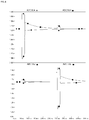
- simulated voltage curves shown in time domain represent the signals at the ADC inputs 31 , which the detection of the touch and recognition of the touched piezoelectric sensor element 11 is based on.
- the voltage curves are captured from a single touch recognition test, where piezoelectric sensor element 11 A of FIG. 1 is pressed at 50 msec, for 20 msec period, and piezoelectric sensor element 11 H of the same FIG. 1 is pressed at 300 msec, for 20 msec period.
- the upper curves indicate the detected signals originated from piezoelectric sensor element 11 A at row of piezoelectric sensor element matrix 10 which is connected to ADC 31 A, and detected signals originated from the same piezoelectric sensor element 11 A at column of piezoelectric sensor element matrix 10 , which is connected to ADC 31 H of FIG. 1 .
- the lower curves indicate the signals originated from piezoelectric sensor element 11 H connected to row and column of the matrix 10 , as detected at ADC 31 B and ADC 31 E of FIG. 1 , respectively.
- the larger difference of the piezoelectric sensor element 11 originated signal amplitudes of a column and a row of the piezoelectric sensor element matrix 10 is found at the ADCs 31 , in comparison to any other piezoelectric sensor element 11 originated signal differences of other columns and rows in the piezoelectric sensor element matrix 10 , or to predetermined reference value stored in controller 30 .
- touch detection is made based on large enough signal difference measured by ADC 31 from the column and row of the matrix 10 , which exceed the signal difference of other columns and rows of the matrix 10 measured by ADC 31 , and/or a set sensitivity threshold for touch detection stored in controller 30 .
- the other ADCs 31 connected to rows and columns of the matrix 10 where the piezoelectric sensor elements 11 are not touched, detect significantly lower signals in comparison to the ADCs 31 connected to the rows and columns of the matrix 10 where the piezoelectric sensor element 11 is touched. This is indicated in FIG. 6 by signals of ADC 31 A and 31 H at 300 msec, upper curves, and ADC 31 B and 31 E at 50 msec, lower curves.
- ADC 31 A and 31 H at 300 msec, upper curves
- ADC 31 B and 31 E at 50 msec, lower curves.
- the different and adjustable sensitivity thresholds can be used for recognition of different kind of touch events in the microcontroller 30 .
- the device comprise a processor, such as the microcontroller 30 , configured by the program code when executed to execute the embodiments of the operations and functionality described.
- the functionality described herein can be performed, at least in part, by one or more hardware logic components.
- illustrative types of hardware logic components include Field-programmable Gate Arrays (FPGAs), Program-specific Integrated Circuits (ASICs), Program-specific Standard Products (ASSPs), System-on-a-chip systems (SOCs), Complex Programmable Logic Devices (CPLDs), Graphics Processing Units (CPUs).
Landscapes
- Engineering & Computer Science (AREA)
- General Engineering & Computer Science (AREA)
- Theoretical Computer Science (AREA)
- Human Computer Interaction (AREA)
- Physics & Mathematics (AREA)
- General Physics & Mathematics (AREA)
- Electronic Switches (AREA)
- Position Input By Displaying (AREA)
Abstract
Description
- 10 piezoelectric sensor element matrix, 4 times 4 as an example;
- 11A-11P individual piezoelectric sensor elements, all are alike with manufacturing tolerances;
- 12A-12D channel selection switch to select appropriate row of the matrix for a given ADC input;
- 13A-13D channel selection switch to select appropriate column of the matrix for a given ADC input;
- 14 isolation switch to disconnect two parts of the VREF net into separate
common reference nets common reference nets ADC 33; - 21A-21H signal conditioning filter: bandwidth limitation, amplitude scaling;
- 30 controller device (microcontroller chip) to detect and interpret piezoelectric sensor element signals with HW and SW, and to control the operation and configuration of the system;
- 31A-31H analog-to-Digital converter (ADC) functions inside the
controller 30, wherein one ADC for each input channel of thecontroller 30, or a single ADC, which can be internally multiplexed to several input channels of thecontroller 30; - 32 signal reference bias voltage (VREF) generation for the piezoelectric
sensor element matrix 10 and theADCs 31; - 33 ADC conversion channel to measure voltage difference of
common reference nets - 141 common reference net for the rows of the matrix of
piezoelectric sensor elements 11; - 142 common reference net for the columns of the matrix of
piezoelectric sensor elements 11; - 143 analog comparator to measure voltage difference of
common reference nets - 144 digital input of the
controller device 30, to monitor output of 143; - 145 resistor with high ohmic value, for example 560 kOhm, to provide
common reference nets switch 14 is disconnected; - 15 wire from of piezoelectric
sensor element matrix 10 to signalconditioning filter 21, either related to a row or a column; - 21 piezoelectric sensor element signal conditioning filter: bandwidth limitation, amplitude scaling;
- 22, 23 piezoelectric sensor element signal scaling resistors, as voltage divider circuit to attenuate incoming signal, wherein values of
resistors resistor 22 shorted andresistor 23 removed, according to the desired signal scaling; - 24 resistor, to make low pass frequency filter together with
capacitor 25, wherein value can be changed according to the desired characteristics; - 25 capacitor, to make low pass frequency filter together with
resistor 24, wherein value can be changed according to the desired characteristics. - 35 power supply voltage of the
controller device 30; - 36A, 36B reference voltage generation circuitry to provide adequate level for the common reference net 140;
- 37 ground level of the
controller device 30; - 140 common reference net for the
piezoelectric sensor element 11 signals.
Claims (18)
Priority Applications (1)
| Application Number | Priority Date | Filing Date | Title |
|---|---|---|---|
| US16/308,114 US10761638B2 (en) | 2016-06-09 | 2017-06-09 | Detection of piezoelectric sensor elements |
Applications Claiming Priority (3)
| Application Number | Priority Date | Filing Date | Title |
|---|---|---|---|
| US201662347609P | 2016-06-09 | 2016-06-09 | |
| US16/308,114 US10761638B2 (en) | 2016-06-09 | 2017-06-09 | Detection of piezoelectric sensor elements |
| PCT/EP2017/064127 WO2017212028A1 (en) | 2016-06-09 | 2017-06-09 | Detection of piezoelectric sensor elements |
Publications (2)
| Publication Number | Publication Date |
|---|---|
| US20190179472A1 US20190179472A1 (en) | 2019-06-13 |
| US10761638B2 true US10761638B2 (en) | 2020-09-01 |
Family
ID=59091484
Family Applications (1)
| Application Number | Title | Priority Date | Filing Date |
|---|---|---|---|
| US16/308,114 Active US10761638B2 (en) | 2016-06-09 | 2017-06-09 | Detection of piezoelectric sensor elements |
Country Status (4)
| Country | Link |
|---|---|
| US (1) | US10761638B2 (en) |
| EP (1) | EP3469467B1 (en) |
| CN (1) | CN109313518B (en) |
| WO (1) | WO2017212028A1 (en) |
Families Citing this family (8)
| Publication number | Priority date | Publication date | Assignee | Title |
|---|---|---|---|---|
| FR3057367B1 (en) * | 2016-10-10 | 2018-11-09 | Commissariat A L'energie Atomique Et Aux Energies Alternatives | DEVICE FOR LOCATING AN IMPACT AGAINST AN INTERACTIVE SURFACE, CORRESPONDING COMPUTER PROGRAM AND PROGRAM |
| WO2019069655A1 (en) * | 2017-10-02 | 2019-04-11 | アルプスアルパイン株式会社 | Input device |
| FI20195169A1 (en) * | 2019-03-07 | 2020-09-08 | Aito Bv | Touch detection device and method |
| FI20195168A1 (en) | 2019-03-07 | 2020-09-08 | Aito Bv | Matrix of haptic elements |
| GB2593607B (en) * | 2019-09-06 | 2022-04-27 | Cirrus Logic Int Semiconductor Ltd | Force sensing circuitry |
| FI20205146A1 (en) * | 2020-02-12 | 2021-08-13 | Aito Bv | A piezoelectric sensing device |
| FI20215120A1 (en) * | 2021-02-04 | 2022-08-05 | Aito Bv | Piezoelectric sensor device |
| CN120949919B (en) * | 2025-10-15 | 2026-01-30 | 上海轩辕文化科技有限公司 | Method for reducing power consumption of pressure sensing screen |
Citations (9)
| Publication number | Priority date | Publication date | Assignee | Title |
|---|---|---|---|---|
| EP0933873A1 (en) | 1998-01-30 | 1999-08-04 | Dynalab AG | Piezoelectric keyboard |
| US20020053857A1 (en) * | 2000-03-23 | 2002-05-09 | Scott Walter G. | Piezoelectric identification device and applications thereof |
| US20050174015A1 (en) * | 2000-03-23 | 2005-08-11 | Scott Walter G. | Multiplexer for a piezo ceramic identification device |
| US20090250267A1 (en) * | 2008-04-02 | 2009-10-08 | Immersion Corp. | Method and apparatus for providing multi-point haptic feedback texture systems |
| EP2144138A1 (en) | 2008-07-07 | 2010-01-13 | Sensitive Object | Device for changing the operational state of an apparatus |
| EP2315101A1 (en) | 2009-10-02 | 2011-04-27 | Research In Motion Limited | A method of waking up and a portable electronic device configured to perform the same |
| US8810105B2 (en) | 2010-06-15 | 2014-08-19 | Aito B.V. | Apparatus and method for reducing energy consumption in monitoring means of a plurality of piezoelectric components |
| US20150123931A1 (en) * | 2013-11-04 | 2015-05-07 | Qualcomm Incorporated | Piezoelectric force sensing array |
| DE102014107786A1 (en) | 2014-06-03 | 2015-12-03 | Industrial Science GmbH powered by IAV | Method for evaluating the measured values of active sensor elements |
Family Cites Families (8)
| Publication number | Priority date | Publication date | Assignee | Title |
|---|---|---|---|---|
| US4701676A (en) * | 1985-12-18 | 1987-10-20 | Gibson John A | Touch control adaptor |
| US8217809B2 (en) * | 2010-06-22 | 2012-07-10 | Microsoft Corporation | Low power sensing via resistive sensor matrix |
| KR101341924B1 (en) * | 2011-10-21 | 2013-12-19 | 포항공과대학교 산학협력단 | capacitance-measuring type touch sensor |
| US9606606B2 (en) * | 2013-06-03 | 2017-03-28 | Qualcomm Incorporated | Multifunctional pixel and display |
| US9213434B2 (en) * | 2013-07-17 | 2015-12-15 | Nokia Technologies Oy | Piezoelectric actuator and method |
| US8779919B1 (en) * | 2013-11-03 | 2014-07-15 | Instant Care, Inc. | Event communication apparatus and method |
| CN105005016B (en) * | 2015-07-06 | 2018-06-29 | 浙江涵普电力科技有限公司 | A kind of three-phase electric energy meter on-site check system and its method |
| CN105630240B (en) * | 2015-12-23 | 2018-08-07 | 广州中国科学院先进技术研究所 | A kind of multi-point touch panel based on piezoelectric material |
-
2017
- 2017-06-09 US US16/308,114 patent/US10761638B2/en active Active
- 2017-06-09 CN CN201780036072.3A patent/CN109313518B/en active Active
- 2017-06-09 WO PCT/EP2017/064127 patent/WO2017212028A1/en not_active Ceased
- 2017-06-09 EP EP17731500.9A patent/EP3469467B1/en active Active
Patent Citations (12)
| Publication number | Priority date | Publication date | Assignee | Title |
|---|---|---|---|---|
| EP0933873A1 (en) | 1998-01-30 | 1999-08-04 | Dynalab AG | Piezoelectric keyboard |
| US20020053857A1 (en) * | 2000-03-23 | 2002-05-09 | Scott Walter G. | Piezoelectric identification device and applications thereof |
| EP1266346A2 (en) | 2000-03-23 | 2002-12-18 | Cross Match Technologies, Inc. | Piezometric identification device and applications thereof |
| US6720712B2 (en) * | 2000-03-23 | 2004-04-13 | Cross Match Technologies, Inc. | Piezoelectric identification device and applications thereof |
| US20050174015A1 (en) * | 2000-03-23 | 2005-08-11 | Scott Walter G. | Multiplexer for a piezo ceramic identification device |
| US20090250267A1 (en) * | 2008-04-02 | 2009-10-08 | Immersion Corp. | Method and apparatus for providing multi-point haptic feedback texture systems |
| EP2144138A1 (en) | 2008-07-07 | 2010-01-13 | Sensitive Object | Device for changing the operational state of an apparatus |
| US8946973B2 (en) * | 2008-07-07 | 2015-02-03 | Elo Touch Solutions, Inc. | Device for changing the operational state of an apparatus |
| EP2315101A1 (en) | 2009-10-02 | 2011-04-27 | Research In Motion Limited | A method of waking up and a portable electronic device configured to perform the same |
| US8810105B2 (en) | 2010-06-15 | 2014-08-19 | Aito B.V. | Apparatus and method for reducing energy consumption in monitoring means of a plurality of piezoelectric components |
| US20150123931A1 (en) * | 2013-11-04 | 2015-05-07 | Qualcomm Incorporated | Piezoelectric force sensing array |
| DE102014107786A1 (en) | 2014-06-03 | 2015-12-03 | Industrial Science GmbH powered by IAV | Method for evaluating the measured values of active sensor elements |
Non-Patent Citations (2)
| Title |
|---|
| International Search Report for corresponding International Patent Application No. PCT/EP2017/064127 dated Aug. 24, 2017, 4 pages. |
| Written Opinion of the International Searching Authority for corresponding International Patent Application No. PCTEP2017/064127 dated Aug. 24, 2017, 7 pages. |
Also Published As
| Publication number | Publication date |
|---|---|
| WO2017212028A1 (en) | 2017-12-14 |
| EP3469467B1 (en) | 2025-03-12 |
| CN109313518A (en) | 2019-02-05 |
| EP3469467A1 (en) | 2019-04-17 |
| US20190179472A1 (en) | 2019-06-13 |
| CN109313518B (en) | 2022-05-10 |
Similar Documents
| Publication | Publication Date | Title |
|---|---|---|
| US10761638B2 (en) | Detection of piezoelectric sensor elements | |
| US10860152B2 (en) | Capacitance detection circuit, touch apparatus and terminal device | |
| US11561661B2 (en) | Capacitive sensor filtering apparatus, method, and system | |
| CN101369195B (en) | Power effective capacitance detection method and module | |
| US10408862B2 (en) | Multiple channel capacitive voltage divider scanning method and apparatus | |
| KR101488008B1 (en) | Control circuit and control method for touch panel | |
| TW201041305A (en) | Capacitive touch sensing and light emitting diode drive matrix | |
| WO2011037694A1 (en) | Capacitive key touch sensing using analog inputs and digital outputs | |
| EP3482342A1 (en) | Fingerprint sensing system with finger detection | |
| US8508499B2 (en) | Touch sensing circuits and methods for detecting touch events | |
| US9442609B2 (en) | Sensing method and circuit for use with capacitive sensing devices | |
| CN101599770B (en) | Keyboard and keyboard checking method | |
| US20120139867A1 (en) | Capacitive touch apparatus | |
| CN113949373A (en) | Contact detection circuit using different currents for charging and discharging and operation method thereof | |
| EP2722988A1 (en) | A method of the touch detection for capacitive touch sensors | |
| EP3586218B1 (en) | Detecting mechanical interactions | |
| CN207650779U (en) | Circuit and touch screen controller integrated circuit | |
| US12487261B2 (en) | Interference-insensitive determination of a capacitance | |
| US20200241726A1 (en) | Methods and apparatus for a touch sensor | |
| CN113655917A (en) | Capacitive sensing | |
| CN117914327A (en) | Ghost key preventing circuit |
Legal Events
| Date | Code | Title | Description |
|---|---|---|---|
| AS | Assignment |
Owner name: AITO BV, NETHERLANDS Free format text: ASSIGNMENT OF ASSIGNORS INTEREST;ASSIGNORS:KESKI-JASKARI, TURO;RIIHIAHO, JUKKA;REEL/FRAME:047708/0318 Effective date: 20181126 |
|
| FEPP | Fee payment procedure |
Free format text: ENTITY STATUS SET TO UNDISCOUNTED (ORIGINAL EVENT CODE: BIG.); ENTITY STATUS OF PATENT OWNER: LARGE ENTITY |
|
| FEPP | Fee payment procedure |
Free format text: ENTITY STATUS SET TO SMALL (ORIGINAL EVENT CODE: SMAL); ENTITY STATUS OF PATENT OWNER: LARGE ENTITY |
|
| STPP | Information on status: patent application and granting procedure in general |
Free format text: DOCKETED NEW CASE - READY FOR EXAMINATION |
|
| STPP | Information on status: patent application and granting procedure in general |
Free format text: NON FINAL ACTION MAILED |
|
| STPP | Information on status: patent application and granting procedure in general |
Free format text: RESPONSE TO NON-FINAL OFFICE ACTION ENTERED AND FORWARDED TO EXAMINER |
|
| STPP | Information on status: patent application and granting procedure in general |
Free format text: NOTICE OF ALLOWANCE MAILED -- APPLICATION RECEIVED IN OFFICE OF PUBLICATIONS |
|
| FEPP | Fee payment procedure |
Free format text: ENTITY STATUS SET TO UNDISCOUNTED (ORIGINAL EVENT CODE: BIG.); ENTITY STATUS OF PATENT OWNER: LARGE ENTITY |
|
| STCF | Information on status: patent grant |
Free format text: PATENTED CASE |
|
| MAFP | Maintenance fee payment |
Free format text: PAYMENT OF MAINTENANCE FEE, 4TH YEAR, LARGE ENTITY (ORIGINAL EVENT CODE: M1551); ENTITY STATUS OF PATENT OWNER: LARGE ENTITY Year of fee payment: 4 |