US10747924B2 - Method for manufacturing integrated circuit with aid of pattern based timing database indicating aging effect - Google Patents
Method for manufacturing integrated circuit with aid of pattern based timing database indicating aging effect Download PDFInfo
- Publication number
- US10747924B2 US10747924B2 US16/191,172 US201816191172A US10747924B2 US 10747924 B2 US10747924 B2 US 10747924B2 US 201816191172 A US201816191172 A US 201816191172A US 10747924 B2 US10747924 B2 US 10747924B2
- Authority
- US
- United States
- Prior art keywords
- timing
- static probability
- circuit
- circuit cell
- pattern
- Prior art date
- Legal status (The legal status is an assumption and is not a legal conclusion. Google has not performed a legal analysis and makes no representation as to the accuracy of the status listed.)
- Active, expires
Links
Images


Classifications
-
- G—PHYSICS
- G06—COMPUTING OR CALCULATING; COUNTING
- G06F—ELECTRIC DIGITAL DATA PROCESSING
- G06F30/00—Computer-aided design [CAD]
- G06F30/30—Circuit design
- G06F30/32—Circuit design at the digital level
- G06F30/33—Design verification, e.g. functional simulation or model checking
- G06F30/3308—Design verification, e.g. functional simulation or model checking using simulation
- G06F30/3312—Timing analysis
-
- H01L21/82—
-
- H—ELECTRICITY
- H03—ELECTRONIC CIRCUITRY
- H03K—PULSE TECHNIQUE
- H03K19/00—Logic circuits, i.e. having at least two inputs acting on one output; Inverting circuits
- H03K19/20—Logic circuits, i.e. having at least two inputs acting on one output; Inverting circuits characterised by logic function, e.g. AND, OR, NOR, NOT circuits
-
- H—ELECTRICITY
- H10—SEMICONDUCTOR DEVICES; ELECTRIC SOLID-STATE DEVICES NOT OTHERWISE PROVIDED FOR
- H10D—INORGANIC ELECTRIC SEMICONDUCTOR DEVICES
- H10D84/00—Integrated devices formed in or on semiconductor substrates that comprise only semiconducting layers, e.g. on Si wafers or on GaAs-on-Si wafers
- H10D84/01—Manufacture or treatment
-
- G—PHYSICS
- G06—COMPUTING OR CALCULATING; COUNTING
- G06F—ELECTRIC DIGITAL DATA PROCESSING
- G06F2119/00—Details relating to the type or aim of the analysis or the optimisation
- G06F2119/12—Timing analysis or timing optimisation
Definitions
- the present disclosure relates to circuit design and, more particularly, to a method for manufacturing an integrated circuit with the aid of a pattern based timing database indicating aging effects.
- Device aging refers to device performance degradation over time. For example, when a constant electric field is applied to a gate of a transistor, a phenomenon called negative bias temperature instability (NBTI) can cause a buildup of charge in a gate dielectric, which in turn degrades a threshold voltage of the transistor. As a result, transistor aging caused by NBTI can lead to low switching speeds and cell delay degradation over time. Other degenerative mechanisms, such as hot carrier injection (HCl) and time-dependent dioxide breakdown (TDDB), can also cause transistor aging.
- HCl hot carrier injection
- TDDB time-dependent dioxide breakdown
- FinFET fin field-effect transistor
- FIG. 1 illustrates an exemplary system for manufacturing an integrated circuit in accordance with some embodiments of the present disclosure.
- FIG. 2A and FIG. 2B illustrate an exemplary characterization of the pattern based timing database shown in FIG. 1 in accordance with some embodiments of the present disclosure.
- FIG. 3 illustrates an exemplary timing library format of the pattern based timing database shown in FIG. 1 in accordance with some embodiments of the present disclosure.
- FIG. 4 illustrates a flow chart of an exemplary method for determining timing constraints of an integrated circuit in accordance with some embodiments of the present disclosure.
- FIG. 5 illustrates at least a portion of an exemplary integrated circuit designed using the method shown in FIG. 4 in accordance with some embodiments of the present disclosure.
- FIG. 6 illustrates an exemplary operation involved in determining timing constraints of the integrated circuit shown in FIG. 5 in accordance with some embodiments of the present disclosure.
- FIG. 7 illustrates an exemplary operation involved in determining timing constraints of the integrated circuit shown in FIG. 5 in accordance with some embodiments of the present disclosure.
- FIG. 8A and FIG. 8B illustrate an exemplary operation involved in determining timing constraints of the integrated circuit shown in FIG. 5 in accordance with some embodiments of the present disclosure.
- FIG. 9A and FIG. 9B illustrate an exemplary operation involved in determining timing constraints of the integrated circuit shown in FIG. 5 in accordance with some embodiments of the present disclosure.
- FIG. 10A and FIG. 10B illustrate an exemplary operation involved in determining timing constraints of the integrated circuit shown in FIG. 5 in accordance with some embodiments of the present disclosure.
- FIG. 11 is a flow chart of an exemplary method for manufacturing an integrated circuit in accordance with some embodiments of the present disclosure.
- first and second features are formed in direct contact
- additional features may be formed between the first and second features, such that the first and second features may not be in direct contact
- present disclosure may repeat reference numerals and/or letters in the various examples. This repetition is for the purpose of simplicity and clarity and does not in itself dictate a relationship between the various embodiments and/or configurations discussed.
- a signal is asserted with a logical high value to activate a corresponding device when the device is active high.
- the signal is deasserted with a low logical value to deactivate the corresponding device.
- the signal is asserted with a low logical value to activate the device, and is deasserted with a high logical value to deactivate the device.
- extra timing margins can be added in the circuit design.
- the added timing margin is derived based on an end-of-life (EOL) approach, which assumes each device element, such as a transistor, suffers identical degradation. Device degradation can be estimated according to at least one of voltage, temperature, life cycle and percentile analyses.
- EOL end-of-life
- implementing an integrated circuit with the EOL approach may produce an over-constrained design because of ignorance of the real circuit usage profile and aging sensitivity difference in standard cell pins.
- the over-constrained design uses pessimistic and excessive aging margins for guard-banding potential timing violations due to aging.
- respective delay times of different device elements in the over-constrained design are characterized by a timing library or flat guard-banding formats, wherein the timing library is constructed with high percentile device degradation and worst-case stress.
- the excessive aging margins often penalize a circuit design having low performance, high power and big area, and also becomes a burden to advanced technology nodes.
- the present disclosure describes exemplary methods for manufacturing integrated circuits with the aid of a pattern based timing database, also referred to as an input stress based aging timing database.
- the pattern based timing database can be created by taking into account circuit usage profiles and circuit topologies of the integrated circuits. As a result, a timing margin of an integrated circuit manufactured using the exemplary methods would be more realistic, which improves circuit performance.
- the exemplary methods may derive the pattern based timing database as a function of static probability (SP) information. Since a static probability of a circuit pin can indicate a probability that a signal at the circuit pin is at a predetermined logic state, the static probability of the circuit pin can reflect input stress imposed thereon in a circuit usage profile. It is worth noting that aging effects on a circuit cell, such as a standard cell or a logic gate, in an integrated circuit will vary in response to input stress imposed thereon. Hence, when a delay of a timing arc of a circuit cell, such as a standard cell or a logic gate, in an integrated circuit is determined according to a static probability of the circuit cell, the integrated circuit can have an optimized or more realistic timing margin.
- SP static probability
- the exemplary methods may use pin sensitivity information as well as static probability information of incoming nets to decide connectivity, with an objective to mitigate aging effects on logic circuit performance with low area overhead.
- the pattern based timing database may indicate respective timing arc delays of different circuit pins of a circuit cell.
- a circuit designer or a design tool utilizing the exemplary methods can connect a highly sensitive pin to a low stress probability signal, and connect a less sensitive pin to a high stress probability signal to mitigate performance impact due to aging.
- timing margin of the integrated circuit can be more realistic and hence reduce pessimistic assumption in existing methodology. Further description is provided below.
- FIG. 1 illustrates an exemplary system for manufacturing an integrated circuit in accordance with some embodiments of the present disclosure.
- the system 100 can utilize a circuit usage profile and a circuit topology of the integrated circuit (not shown in FIG. 1 ) to determine a more realistic or optimized timing margin thereof, thereby mitigating aging impacts on circuit performance.
- the system 100 includes, but is not limited, a circuit design system 102 and a circuit generation system 104 .
- the circuit design system 102 is configured to provide design information INF of the integrated circuit for the circuit generation system 104 .
- the circuit generation system 104 is configured to implement the integrated circuit according to the design information INF.
- the circuit generation system 104 is configured to form a circuit on a substrate using a plurality of photomasks in a multi-patterning deposition process and/or other suitable circuit manufacturing process.
- the circuit design system 102 includes, but is not limited to, a control circuit 110 , a storage unit 120 and an input/output (I/O) module 130 .
- the control circuit 110 including at least one processor or at least one controller, is operative to control operations of the circuit design system 102 .
- the control circuit 110 may include central processing unit(s), graphic processing unit(s), general purpose processor(s), digital signal processor(s), microprocessor(s) or other types of processors.
- the control circuit 110 may include microcontroller(s), application specific integrated circuit(s), field programmable gate array(s), programmable logic device(s) or other types of controllers.
- the storage unit 120 may include any computer-readable media capable of storing data, instructions, software programs, or combinations thereof.
- the storage unit 120 may be implemented by a memory device including a read-only memory (ROM), a random access memory (RAM), a flash memory, a content addressable memory (CAM), a disk memory, a memory card or any other types of memory devices suitable for storing information.
- the storage unit 120 may store computer program code PROG, i.e. a set of execution instructions, that causes the control circuit 110 to execute operation of a circuit design tool 112 such as computer aided design (CAD) tool or an electronic design automation (EDA) tool.
- the storage unit 120 may also store a design database 124 for operation of the circuit design tool 112 .
- the I/O module 130 can be configured to receive input signals for designing the integrated circuit, and output associated information during a design process.
- the I/O module 130 may include a keyboard, a mouse, a display, a touch screen, other types of I/O devices, or combinations thereof.
- the control circuit 110 may control the I/O module 130 to display a graphic user interface associated with the circuit design tool 112 launching in the circuit design system 102 .
- the design database 122 may include a physical design database PDB and a pattern based timing database TDB.
- the physical design database PDB may include information associated with placement of circuit cells, timing constraints, area constraints, power constraints and floorplan information.
- the pattern based timing database TDB may indicate timing arc delays of circuit cells under different input stress conditions.
- the circuit design system 102 or the circuit design tool 112 launching in the circuit design system 102 , may update timing constraint information stored in the physical design database PDB according to the pattern based timing database TDB.
- the pattern based timing database TDB may indicate respective reference delays of timing arcs of a circuit cell characterized in response to different input stress patterns. It is worth noting that as input stress imposed on the circuit cell may differ in different circuit usage profiles, the reference delays of the timing arcs can serve as timing arc delays of the circuit cell in different circuit usage profiles.
- the circuit design system 102 can determine a suitable timing arc delay for each circuit cell in the integrated circuit. The circuit design system 102 may update the timing constraints of the integrated circuit according to the determined timing arc delay. As a result, the design information INF provided for the circuit generation system 104 can indicate a suitable timing margin for the integrated circuit.
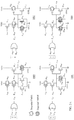
- FIG. 2A and FIG. 2B illustrate an exemplary characterization of the pattern based timing database TDB shown in FIG. 1 in accordance with some embodiments of the present disclosure.
- the characterization shown in FIG. 2A and FIG. 2B is described with reference to an OR gate including p-channel metal-oxide-semiconductor (PMOS) transistors M PA , M PB and M PZ , and n-channel metal-oxide-semiconductor (NMOS) transistors M NA , M NB and M Nz .
- PMOS metal-oxide-semiconductor
- NMOS n-channel metal-oxide-semiconductor
- the pattern based timing database TDB shown in FIG. 1 can include other timing libraries or sub-databases associated with various types of circuit cells.
- the number of sub-databases in the pattern based timing database TDB may vary in response to the number of input stress patterns.
- the pattern based timing database TDB may include N sub-databases characterized by N input stress patterns respectively, where N is a positive integer greater than one. Each of the N sub-databases indicates respective reference delays of timing arcs of the circuit cell characterized in response to a corresponding input stress pattern.
- different input stress patterns are applied to input pins A OR and B OR of the OR gate to determine sub-databases DB 0 -DB 3 in the pattern based timing database TDB shown in FIG. 1 .
- the different input stress patterns can represent different use scenarios of the OR gate.
- the input pins A OR and B OR are applied by an input stress pattern “00” to determine the sub-database DB 0 .
- the input stress pattern “00” represents that each of the input pins A OR and B OR is coupled to a low voltage such as a ground voltage GND.
- the PMOS transistor M PA can be labeled a degraded PMOS.
- the PMOS transistor M PB and the NMOS transistor M NZ can be labeled a degraded PMOS and a degraded NMOS, respectively, under an input stress condition where the input stress pattern “00” is applied to the OR gate.
- the input pins A OR and B OR are applied by an input stress pattern “01” to determine the sub-database DB1.
- the input stress pattern “01” represents that the input pins A OR and B OR are respectively coupled to a low voltage and a high voltage such as a supply voltage VDD.
- each of the PMOS transistors M PB and M PZ can be labeled a degraded PMOS
- the NMOS transistor M NA can be labeled a degraded NMOS.
- the PMOS transistor M PZ can be labeled a degraded PMOS
- each of the NMOS transistors M NA and M NB can be labeled a degraded NMOS.
- delays of timing arcs TA 0 -TA 3 of te OR gate are measured under input stress conditions shown in FIG. 2A .
- Each of the timing arcs TA 0 -TA 3 defines signal propagation through the OR gate and a timing relationship between two related pins.
- the timing arc TA 0 defines a timing relationship between the output pin Z OR and the input pin A OR where a low-to-high transition occurs.
- the low-to-high transition occurring at the input pin A OR causes a low-to-high transition occurring at the output pin Z OR .
- the timing arc TA 0 can be represented as “A OR ⁇ Z OR (R) ”.
- the timing arc TA 1 defines a timing relationship between the output pin Z OR and the input pin A OR where a high-to-low transition occurs.
- the timing arc TA 2 represented as “B OR ⁇ Z OR (R) ”, defines a timing relationship between the output pin Z OR and the input pin B OR where a low-to-high transition occurs;
- the timing arc TA 3 represented as “B OR ⁇ Z OR (F) ”, defines a timing relationship between the output pin Z and the input pin B where a high-to-low transition occurs.
- the sub-database DB 0 indicates four reference delays DL 00 , DL 01 , DL 02 and DL 03 , which are delay times of the timing arcs TA 0 -TA 3 measured under an input stress condition where the OR gate is applied by the input stress pattern “00”.
- the sub-database DB 1 indicates four reference delays DL 10 , DL 11 , DL 12 and DL 13 , which are delay times of the timing arcs TA 0 -TA 3 measured under an input stress condition where the OR gate is applied by the input stress pattern “01”.
- the sub-database DB 2 indicates reference aging delays DL 20 , DL 21 , DL 22 and DL 23 , which are delay times of the timing arcs TA 0 -TA 3 measured under an input stress condition where the OR gate is applied by the input stress pattern “10”.
- the sub-database DB 3 indicates four reference delays DL 30 , DL 31 , DL 32 and DL 33 , which are delay times of the timing arcs TA 0 -TA 3 measured under an input stress condition where the OR gate is applied by the input stress pattern “11”.
- each sub-database can indicate respective reference delays of the timing arc TA 0 -TA 3 under a corresponding input stress condition
- the sub-databases DB 0 -DB 3 can indicate reference delays of each timing arc under different input stress conditions.
- the reference delays DL 00 , DL 10 , DL 20 and DL 30 of the timing arc TA 0 respectively corresponding to the input stress patterns “00”, “01”, “10” and “11”, can be provided by the sub-databases DB 0 -DB 3 .
- the reference delays DL 00 , DL 10 , DL 20 and DL 30 of the timing arc TA 0 can reflect different aging effects on the OR gate in different circuit usage profiles.
- reference delays of timing arcs can be stored in a timing library format expression or in any other suitable format.
- FIG. 3 illustrates an exemplary timing library format of the pattern based timing database TDB shown in FIG. 1 in accordance with some embodiments of the present disclosure.
- the timing library format shown in FIG. 3 can represent an embodiment of a timing library format for reference delays of each timing arc shown in FIG. 2A and FIG. 2B .
- “pattern” syntax represents an input stress pattern used to characterize reference delays.
- “!A1 !A2”, “!A1 A2”, “A1 !A2” and “A1 A2” can represent the input stress patterns “00”, “01”, “10” and “11”, respectively.
- a reference delay characterized in response to the input stress patterns “00”, represented by “!A1 !A2”, is expressed in a derate format with device characteristics including input slew rates and output loads.
- “index_1” represents an input slew index at a slow corner (“late”)
- “index_2” represents an output load index
- “values” represents candidate derating factors of the reference delay.
- the reference delay may correspond to nine candidate derating factors.
- Other reference delays, characterized in response to the input stress patterns “01”, “10” and “11” respectively, can be expressed in a similar/identical derate format.
- the timing delay, or the reference delay is equal to a corresponding derating factor multiplied by a base delay of the timing arc.
- the base delay is characterized without applying the input stress patterns “00”, “01”, “10” and “11” to the circuit cell.
- static probability information of an integrated circuit can be used to reflect a circuit usage file of the integrated circuit.
- a static probability at a circuit pin can indicate a probability that a signal received at the circuit pin is at a predetermined logic state.
- a static probability indicating that a signal is at a logic high state can be referred to as SP1
- a static probability indicating that a signal is at a logic low state can be referred to as SP0
- the static probability information e.g. respective static probabilities of circuit pins in the integrated circuit, can serve as information regarding the circuit usage file of the integrated circuit. By taking into account the static probability information, a timing margin of the integrated circuit would be more realistic.
- FIG. 4 illustrates a flow chart of an exemplary method for determining timing constraints of an integrated circuit in accordance with some embodiments of the present disclosure.
- the method 400 can be employed in the circuit design system 102 shown in FIG. 1 to determine a more realistic timing margin, or aging timing margin, of the integrated circuit. However, this is not intended to limit the scope of the present disclosure.
- the method 400 can be employed in other systems for manufacturing an integrated circuit to determine more realistic timing margins.
- FIG. 5 illustrates at least a portion of an exemplary integrated circuit designed using the method 400 shown in FIG. 4 , in accordance with some embodiments of the present disclosure.
- FIG. 6 to FIG. 10B illustrate operations involved in determining timing constraints of the integrated circuit shown in FIG. 5 in accordance with some embodiments of the present disclosure.
- the method 400 can be used to design other circuit topologies without departing from the scope of the present disclosure.
- other operations in the method 400 can be performed.
- operations of the method 400 can be performed in a different order and/or vary.
- a timing path of the integrated circuit is determined.
- the timing path passes through a set of circuit cells of the integrated circuit.
- the circuit design tool 112 may place and route circuit cells of the integrated circuit 500 , which includes a NOR gate G 1 , a NOR gate G 2 and a NAND gate G 3 .
- the NOR gate G 1 has an input pin A G1 , an input pin B G1 and an output pin Z G1 .
- the NOR gate G 2 has an input pin A G2 , an input pin B G2 and an output pin Z G2 .
- the NAND gate G 3 has an input pin A G3 , an input pin B G3 and an output pin Z G3 .
- the circuit design tool 112 may determine a timing path TP according to the physical design database PDB.
- the timing path TP may be, but is not limited to, a critical path which is a path between an input and an output of the integrated circuit 500 with the maximum delay.
- the timing path TP includes a plurality of timing arcs TA G1 -TA G3 .
- the timing arc TA G1 models a timing delay of 24.94 picoseconds (ps) that a signal takes to propagate from the input pin B G1 to the output pin Z G1 where a low-to-high transition occurs.
- the timing arc TA G2 models a delay of 24.94 ps that a signal takes to propagate from the input pin B G2 to the output pin Z G2 where a low-to-high transition occurs.
- the timing arc TA G3 models a delay of 19.4 ps that a signal takes to propagate from the input pin B G3 to the output pin Z G3 where a high-to-low transition occurs.
- the physical design database PDB indicates that the timing path TP has a path delay of 69.28 ps.
- these predetermined delays indicated by the physical design database PDB i.e. 24.94 ps and 19.4 ps, may be worst-case delays.
- the first static probability indicates a probability that a signal received at the input pin in the timing path is at a predetermined logic state.
- the circuit design tool 112 may determine respective first static probabilities at the input pins A G1 , B G1 , A G2 and A G3 , i.e. 0.9, 0.1, 0.05 and 0.091, based on a circuit usage profile indicated by the physical design database PDB.
- each of the first static probabilities is SP1, which indicates a probability that a signal received at a corresponding input pin is at a logic high state.
- the circuit design tool 112 may use associated logistic equations to calculate respective first static probabilities of the other input pins B G2 and B G3 .
- a static probability pattern of the circuit cell is generated according to a first static probability at each input pin of the circuit cell.
- the static probability pattern can be implemented to include a rounding value of each first static probability of the circuit cell.
- the circuit design tool 112 may round a first static probability at an input pin to determine a corresponding second static probability, which is equal to either a first probability value or a second probability value different from the first probability value.
- Each second static probability of the circuit cell can serve as at least a portion of a static probability pattern of the circuit cell.
- the circuit design tool 112 may determine a second static probability by comparing a corresponding first static probability with a predetermined static probability.
- the second static probability is set to the first probability value such as 1.
- the first static probability is not greater than the predetermined static probability
- the second static probability is set to the second probability value such as 0.
- the predetermined static probability is set to 0.5
- the first static probabilities at the input pins A G1 and B G1 i.e. 0.9 and 0.1, can be rounded to 1 and 0 respectively, and a static probability pattern of the NOR gate G 1 can be represented as “10”.
- a static probability pattern of the NOR gate G 2 can be represented as “00”
- a static probability pattern of the NAND gate G 3 can be represented as “01”.
- a pattern based timing database also referred to as an input stress based aging timing database
- the pattern based timing database can indicate reference timing arc delays of the circuit cells, such as standard cells, under different input stress conditions.
- the pattern based timing database TDB can be characterized to indicate a plurality of reference delays of each timing arc of a circuit cell.
- the reference delays can be characterized in response to a plurality of input stress patterns applied to the circuit cell respectively.
- each of the sub-databases DB 0 -DB 3 can be characterized by measuring respective reference delays of the timing arcs TA 0 -TA 3 under different input stress conditions.
- respective reference delays of each timing arc can be characterized in response to the input stress patterns “00”, “01”, “10” and “11” respectively.
- different input stress patterns can be applied to a reference circuit cell, such as a NOR gate or a NAND gate, to characterize respective reference delays of each timing arc of the NOR gate G 1 , the NOR gate G 2 and the NAND gate G 3 of the integrated circuit 400 shown in FIG. 7 .
- the pattern based timing database is derived.
- the pattern based timing database TDB is derived and stored in the storage unit 120 .
- At operation 422 at least one of timing delays of the circuit cells along the timing path is updated according to the static probability pattern and the pattern based timing database.
- the circuit design tool 112 may update at least one of respective timing delays of the NOR gate G 1 , the NOR gate G 2 and the NAND gate G 3 according to reference delays indicated by the pattern based timing database TDB.
- respective reference delays of a timing arc “B NR ⁇ Z NR (R)” of a NOR gate are characterized in response to input stress patterns “00”, “01”, “10” and “10” applied to input pins B NR and A NR .
- Respective reference delays of a timing arc “B NA ⁇ Z NA (F)” of a NAND gate are characterized in response to input stress patterns “00”, “01”, “10” and “10” applied to input pins B NA and A NA .
- the reference delays of the timing arc “BR NR ⁇ Z NR (R)” can serve as reference delays of the timing arc TA G1 of the NOR gate G 1 , as well as reference delays of the timing arc TA G2 of the NOR gate G 2 , shown in FIG. 8B .
- respective reference delays of the timing arc “B NA ⁇ Z NA (F)” shown in FIG. 8A can serve as reference delays of the timing arc TA G3 of the NAND gate G 3 shown in FIG. 8B .
- the timing delay of the NOR gate G 1 along the timing path can be updated from the predetermined delay of 24.94 ps to a reference delay of 24 ps, which is characterized in response to the input stress pattern “01” matching the static probability pattern of the NOR gate G 1 .
- the circuit design tool 112 shown in FIG. 1 may select a sub-database from the pattern based timing database TDB characterized in response to the input stress pattern “01”, thereby setting the timing delay of the NOR gate G 1 to the reference delay of 24 ps indicated in the sub-database.
- the timing delay of the NAND gate G 3 along the timing path can be updated from the predetermined delay of 19.4 ps to a reference delay of 17.6 ps, which is characterized in response to the input stress pattern “10” matching the static probability pattern of the NAND gate G 3 .
- the path delay of the timing path TP can be updated to 66.54 ps accordingly.
- the circuit design tool 112 can determine a more realistic timing margin, thus improving circuit performance of the integrated circuit 500 .
- a timing margin of the integrated circuit is optimized at least according to a circuit topology thereof.
- the circuit design tool 112 may update at least one of respective timing delays of the NOR gate G 1 , the NOR gate G 2 and the NAND gate G 3 according to pin sensitivity or pin connection information indicated by the pattern based timing database TDB.
- a highly sensitive pin can be connected to a low stress probability signal, and a less sensitive pin can be connected to a high stress probability signal to mitigate performance impact due to aging.
- a reference delay of a timing arc “A NR ⁇ Z NR (R)”, which is characterized in response to the input stress pattern “10” complementary to the static probability pattern “01” of the NOR gate G 1 is shorter than the reference delay of the timing arc “B NR ⁇ Z NR (R)”, which is characterized in response to the input stress pattern “01” matching to the static probability pattern “01” of the NOR gate G 1 .
- the input pins A G1 and B G1 of the NOR gate G 1 can be swapped such that a timing arc TA G1 ′, defining a timing relationship between the input pin A G1 and the output pin Z G1 , is included in the timing path TP.
- the timing delay of the NOR gate G 1 can be updated to a reference delay of 21.93 ps for timing optimization.
- the reference delay of the timing arc “B NR ⁇ Z NR (R)” may be indicated in a first sub-database characterized in response to the input stress pattern “01” matching the static probability pattern, and the reference delay of the timing arc “A NR ⁇ Z NR (R)” may be indicated in a second sub-database characterized in response to the input stress pattern “10” complementary to the static probability pattern.
- the 1 may select, from the pattern based timing database TDB, the first sub-database and the second sub-database to determining if a reference delay of the timing arc TA G1 ′ indicated by the second sub-database is shorter than a reference delay of the timing arc TA G1 indicated by the first sub-database.
- a reference delay of a timing arc “A NA ⁇ Z NA (F)” of the NAND gate characterized in response to the input stress pattern “01” complementary to the static probability pattern “10” of the NAND gate G 3 , is shorter than the reference delay of the timing arc “B NA ⁇ Z NA (F)”.
- the input pins A G3 and B G3 of the NNAD gate G 3 can be swapped to update the timing delay of the NAND gate G 3 . Accordingly, the path delay of the timing path TP can be updated to 63.81 ps.
- the pattern based timing database TDB may indicate timing arc delay information of multiple reference circuit cells, which have a same cell type but different device parameters such as cell sizes or transistor threshold voltages. Reference delays of a timing arc of a circuit cell, having a same cell type as the reference circuit cells, can be characterized by applying different input stress patterns to the reference circuit cells. Hence, the timing margin of the integrated circuit can be further optimized according to device parameter information.
- the pattern based timing database TDB shown in FIG. 1 may indicate reference delays of two NOR gates, which are different reference circuit cells having a same cell type but different device parameters D 1 and D 2 .
- Reference delays of timing arcs of the NOR gate G 1 /G 2 can be characterized by applying the input stress patterns to these two NOR gates.
- the NOR gate G 2 can be implemented by the NOR gate exhibiting a reference delay of 23.75 ps for the timing arc “B NR ⁇ Z NR (R)”.
- the path delay of the timing path TP can be updated to 62.62 ps accordingly.
- the two NOR gates shown in FIG. 10A have different transistor threshold voltages.
- the NOR gate G 2 can be implemented by the NOR gate having a lower transistor threshold voltage, thereby reducing the timing delay for the timing arc “B NR ⁇ Z NR (R)”.
- a physical design database is updated.
- the circuit design tool 112 shown in FIG. 1 may update the physical design database PDB by rerouting and legalizing the circuit cells shown in FIG. 10B .
- the design information INF provided to the circuit generation system 104 for circuit manufacturing, can indicate the updated physical design database PDB.
- various rounding methods can be used in operation 416 to convert first static probabilities of a circuit cell to a static probability pattern thereof.
- the predetermined static probability can be set to a probability value different from 0.5.
- a static probability pattern of a circuit cell is not limited to be represented by a two-bit binary value.
- a static probability pattern of a circuit cell having M input terminals can be represented as an M-bit binary value, where M is an integer.
- a static probability pattern of a circuit cell having three input terminals can be represented as a three-bit binary value.
- FIG. 11 is a flow chart of an exemplary method for manufacturing an integrated circuit in accordance with some embodiments of the present disclosure.
- the method 1100 may be employed in system 100 shown in FIG. 1 , thereby mitigating performance impact on the integrated circuit due to aging.
- the method 1100 can be employed in other systems for manufacturing an integrated circuit without departing from the scope of the present disclosure.
- other operations in the method 1100 can be performed.
- operations of the method 1100 can be performed in a different order and/or vary.
- a static probability pattern of a circuit cell in a timing path of the integrated circuit is determined.
- the circuit design tool 112 when launched by the control circuit 110 , is configured to determine a static probability pattern of each circuit cell in a timing path of an integrated circuit, such as a critical path of the integrated circuit.
- the static probability pattern can indicate a static probability of a signal received at each input pin of the circuit cell.
- the circuit design system 102 can take into account a circuit usage profile of the integrated circuit during the design process.
- at least part of operation 1110 shown in FIG. 11 can be implemented by operations 412 - 416 shown in FIG. 4 .
- a timing delay of the circuit cell along the timing path is determined according to the static probability pattern and a pattern based timing database.
- the pattern based timing database can indicate a plurality of reference delays of each timing arc of the circuit cell characterized in response to a plurality of input stress patterns respectively.
- the timing delay of the NOR gate G 1 along the timing path TP can be set to a reference delay of the timing arc TA G1 , i.e. 24 ps, characterized in response to an input stress pattern matching the static probability pattern “01”.
- a reference delay of the circuit cell along the timing path is determined according to the static probability pattern and a pattern based timing database.
- the pattern based timing database can indicate a plurality of reference delays of each timing arc of the circuit cell characterized in response to a plurality of input stress patterns respectively.
- the timing delay of the NOR gate G 1 along the timing path TP can be set to a reference delay of the timing arc TA G1 , i.e. 24 ps,
- the input pins A G1 and B G1 can be swapped such that the timing arc TA G1 ′ is included in the timing path TP.
- the timing delay of the NOR gate G 1 along the timing path TP can be set to a reference delay of the timing arc TA G1 ′, i.e. 21.93 ps, characterized in response to an input stress pattern complementary to the static probability pattern “01”.
- at least part of operation 1120 shown in FIG. 11 can be implemented by operations 418 - 424 shown in FIG. 4 .
- the integrated circuit is manufactured according to the timing delay of the circuit cell along the timing path.
- the circuit design system 102 may generate the design information INF which indicates the determined timing delay of each circuit cell of the integrated circuit, and the circuit generation system 104 may refer to the design information INF to manufacture the integrated circuit.
- the design information INF can indicate optimized or more realistic timing delays, the integrated circuit can have a more realistic timing margin and improved circuit performance.
- an exemplary method for manufacturing an integrated circuit may set a timing delay of each circuit cell of the integrated circuit according sub-databases included in a pattern based timing database.
- FIG. 12 is a flow chart of an exemplary method for manufacturing an integrated circuit in accordance with some embodiments of the present disclosure.
- the method 1100 may be employed in system 100 shown in FIG. 1 , thereby mitigating performance impact on the integrated circuit due to aging.
- the method 1100 can be employed in other systems for manufacturing an integrated circuit without departing from the scope of the present disclosure.
- other operations in the method 1100 can be performed.
- operations of the method 1100 can be performed in a different order and/or vary.
- the method for manufacturing an integrated circuit can determine timing arc delays in the integrated circuit by taking into account the real circuit usage profile and aging sensitivity difference in standard cell pins. As a result, the timing margin of the integrated circuit can be more realistic, thus improving performance of aging-critical digital designs.
- Some embodiments described herein may include a method for manufacturing an integrated circuit.
- the method includes determining a static probability pattern of a circuit cell in a timing path of the integrated circuit; determining a timing delay of the circuit cell along the timing path according to the static probability pattern and a pattern based timing database, wherein the pattern based timing database indicates a plurality of reference delays of each timing arc of the circuit cell characterized in response to a plurality of input stress patterns respectively; and manufacturing the integrated circuit according to the timing delay of the circuit cell along the timing path.
- Some embodiments described herein may include a method for manufacturing an integrated circuit.
- the method includes determining static probability information of a set of circuit cells in a timing path of the integrated circuit; determining a timing delay of each circuit cell in the set of circuit cells along the timing path according to the static probability information and a pattern based timing database, wherein the pattern based timing database comprises N sub-databases characterized by N input stress patterns respectively, N is a positive integer greater than one, and each of the N sub-databases indicates respective reference delays of timing arcs of the circuit cell characterized in response to a corresponding input stress pattern; and manufacturing the integrated circuit according to the timing delay of the circuit cell along the timing path.
- Some embodiments described herein may include a method for manufacturing an integrated circuit.
- the method includes determining a static probability pattern of a circuit cell in a timing path of the integrated circuit; characterizing N reference delays of a timing arc of the circuit cell in response to N input stress patterns applied to a reference circuit cell respectively, N being an integer greater than one, the reference circuit cell having a same cell type as the circuit cell; setting a timing delay of the circuit cell along the timing path to one of the N reference delays according to the static probability pattern; and manufacturing the integrated circuit according to the timing delay of the circuit cell along the timing path.
Landscapes
- Engineering & Computer Science (AREA)
- Computer Hardware Design (AREA)
- Physics & Mathematics (AREA)
- General Engineering & Computer Science (AREA)
- Theoretical Computer Science (AREA)
- Computing Systems (AREA)
- Mathematical Physics (AREA)
- Evolutionary Computation (AREA)
- Geometry (AREA)
- General Physics & Mathematics (AREA)
- Design And Manufacture Of Integrated Circuits (AREA)
Abstract
Description
Claims (20)
Priority Applications (1)
| Application Number | Priority Date | Filing Date | Title |
|---|---|---|---|
| US16/191,172 US10747924B2 (en) | 2018-07-16 | 2018-11-14 | Method for manufacturing integrated circuit with aid of pattern based timing database indicating aging effect |
Applications Claiming Priority (2)
| Application Number | Priority Date | Filing Date | Title |
|---|---|---|---|
| US201862698556P | 2018-07-16 | 2018-07-16 | |
| US16/191,172 US10747924B2 (en) | 2018-07-16 | 2018-11-14 | Method for manufacturing integrated circuit with aid of pattern based timing database indicating aging effect |
Publications (2)
| Publication Number | Publication Date |
|---|---|
| US20200019663A1 US20200019663A1 (en) | 2020-01-16 |
| US10747924B2 true US10747924B2 (en) | 2020-08-18 |
Family
ID=69138346
Family Applications (1)
| Application Number | Title | Priority Date | Filing Date |
|---|---|---|---|
| US16/191,172 Active 2038-11-17 US10747924B2 (en) | 2018-07-16 | 2018-11-14 | Method for manufacturing integrated circuit with aid of pattern based timing database indicating aging effect |
Country Status (1)
| Country | Link |
|---|---|
| US (1) | US10747924B2 (en) |
Citations (6)
| Publication number | Priority date | Publication date | Assignee | Title |
|---|---|---|---|---|
| US20070143722A1 (en) * | 2005-12-16 | 2007-06-21 | International Business Machines Corporation | System and method of criticality prediction in statistical timing analysis |
| US20070288822A1 (en) * | 2006-04-27 | 2007-12-13 | Xijiang Lin | Timing-aware test generation and fault simulation |
| US20090070714A1 (en) * | 2007-09-10 | 2009-03-12 | Synopsys, Inc. | Identifying And Improving Robust Designs Using Statistical Timing Anaysis |
| US20090119629A1 (en) * | 2007-11-02 | 2009-05-07 | Grise Gary D | System and method for generating at-speed structural tests to improve process and environmental parameter space coverage |
| US20100017774A1 (en) * | 2006-08-31 | 2010-01-21 | Ipflex Inc. | Method and system for mounting circuit design on reconfigurable device |
| US20150254392A1 (en) * | 2014-03-04 | 2015-09-10 | Fujitsu Semiconductor Limited | Layout verification method and verification apparatus |
-
2018
- 2018-11-14 US US16/191,172 patent/US10747924B2/en active Active
Patent Citations (6)
| Publication number | Priority date | Publication date | Assignee | Title |
|---|---|---|---|---|
| US20070143722A1 (en) * | 2005-12-16 | 2007-06-21 | International Business Machines Corporation | System and method of criticality prediction in statistical timing analysis |
| US20070288822A1 (en) * | 2006-04-27 | 2007-12-13 | Xijiang Lin | Timing-aware test generation and fault simulation |
| US20100017774A1 (en) * | 2006-08-31 | 2010-01-21 | Ipflex Inc. | Method and system for mounting circuit design on reconfigurable device |
| US20090070714A1 (en) * | 2007-09-10 | 2009-03-12 | Synopsys, Inc. | Identifying And Improving Robust Designs Using Statistical Timing Anaysis |
| US20090119629A1 (en) * | 2007-11-02 | 2009-05-07 | Grise Gary D | System and method for generating at-speed structural tests to improve process and environmental parameter space coverage |
| US20150254392A1 (en) * | 2014-03-04 | 2015-09-10 | Fujitsu Semiconductor Limited | Layout verification method and verification apparatus |
Also Published As
| Publication number | Publication date |
|---|---|
| US20200019663A1 (en) | 2020-01-16 |
Similar Documents
| Publication | Publication Date | Title |
|---|---|---|
| US6427226B1 (en) | Selectively reducing transistor channel length in a semiconductor device | |
| US8024694B2 (en) | Systematic benchmarking system and method for standardized data creation, analysis and comparison of semiconductor technology node characteristics | |
| CN102741777B (en) | Based on the leakage-power optimization of subregion | |
| Han et al. | A global-local optimization framework for simultaneous multi-mode multi-corner clock skew variation reduction | |
| US20090187868A1 (en) | Design of integrated circuits less susceptible to degradations in transistors caused due to operational stress | |
| CN107403024A (en) | Method for analyzing voltage drop and electromigration of IC and computer readable storage medium | |
| US12073160B1 (en) | Dynamic voltage drop model for timing analysis | |
| US7055121B1 (en) | Method, system, and computer program product for designing an integrated circuit using substitution of standard cells with substitute cells having differing electrical characteristics | |
| US12073159B2 (en) | Computing device and method for detecting clock domain crossing violation in design of memory device | |
| TWI853138B (en) | Multi-bit flip flop circuit and method | |
| Ma et al. | Fast cell library characterization for design technology co-optimization based on graph neural networks | |
| US10103715B2 (en) | Method of laying out a semiconductor device based on switching activity and semiconductor device produced thereby | |
| US20050060676A1 (en) | Semiconductor integrated circuit and method for designing same | |
| CN115618779B (en) | Simulation analysis method considering standard cell aging effect | |
| US20220263508A1 (en) | Threshold logic gates using flash transistors | |
| US8762922B1 (en) | System for reducing leakage power of electronic circuit | |
| US10747924B2 (en) | Method for manufacturing integrated circuit with aid of pattern based timing database indicating aging effect | |
| US11328109B2 (en) | Refining multi-bit flip flops mapping without explicit de-banking and re-banking | |
| US20190384868A1 (en) | Method and apparatus for adaptive voltage scaling to eliminate delay variation of whole design | |
| US12248744B2 (en) | Poly-bit cells | |
| US12307182B2 (en) | Voltage impacts on delays for timing simulation | |
| US12373625B1 (en) | Timing domain based modeling of switching probability and signal correlation | |
| US11621704B2 (en) | Input Schmitt buffer operating at a high voltage using low voltage devices | |
| US20250286543A1 (en) | Flip-flops and integrated circuits including the same | |
| CN117829041A (en) | Method, device, equipment and storage medium for designing chip |
Legal Events
| Date | Code | Title | Description |
|---|---|---|---|
| AS | Assignment |
Owner name: TAIWAN SEMICONDUCTOR MANUFACTURING COMPANY LTD., T Free format text: ASSIGNMENT OF ASSIGNORS INTEREST;ASSIGNORS:PITTU, RAVI BABU;HSU, LI CHUNG;YEH, SUNG-YEN;AND OTHERS;REEL/FRAME:047505/0250 Effective date: 20181016 Owner name: TAIWAN SEMICONDUCTOR MANUFACTURING COMPANY LTD., TAIWAN Free format text: ASSIGNMENT OF ASSIGNORS INTEREST;ASSIGNORS:PITTU, RAVI BABU;HSU, LI CHUNG;YEH, SUNG-YEN;AND OTHERS;REEL/FRAME:047505/0250 Effective date: 20181016 |
|
| FEPP | Fee payment procedure |
Free format text: ENTITY STATUS SET TO UNDISCOUNTED (ORIGINAL EVENT CODE: BIG.); ENTITY STATUS OF PATENT OWNER: LARGE ENTITY |
|
| STPP | Information on status: patent application and granting procedure in general |
Free format text: NON FINAL ACTION MAILED |
|
| STPP | Information on status: patent application and granting procedure in general |
Free format text: NOTICE OF ALLOWANCE MAILED -- APPLICATION RECEIVED IN OFFICE OF PUBLICATIONS |
|
| STPP | Information on status: patent application and granting procedure in general |
Free format text: PUBLICATIONS -- ISSUE FEE PAYMENT VERIFIED |
|
| STCF | Information on status: patent grant |
Free format text: PATENTED CASE |
|
| MAFP | Maintenance fee payment |
Free format text: PAYMENT OF MAINTENANCE FEE, 4TH YEAR, LARGE ENTITY (ORIGINAL EVENT CODE: M1551); ENTITY STATUS OF PATENT OWNER: LARGE ENTITY Year of fee payment: 4 |