US10747659B2 - Flash fast program mode for high definition video recording and high resolution camera burst mode recording - Google Patents
Flash fast program mode for high definition video recording and high resolution camera burst mode recording Download PDFInfo
- Publication number
- US10747659B2 US10747659B2 US15/890,118 US201815890118A US10747659B2 US 10747659 B2 US10747659 B2 US 10747659B2 US 201815890118 A US201815890118 A US 201815890118A US 10747659 B2 US10747659 B2 US 10747659B2
- Authority
- US
- United States
- Prior art keywords
- frame
- matching portion
- segment
- index
- storing
- Prior art date
- Legal status (The legal status is an assumption and is not a legal conclusion. Google has not performed a legal analysis and makes no representation as to the accuracy of the status listed.)
- Active, expires
Links
Images


Classifications
-
- H—ELECTRICITY
- H04—ELECTRIC COMMUNICATION TECHNIQUE
- H04N—PICTORIAL COMMUNICATION, e.g. TELEVISION
- H04N5/00—Details of television systems
- H04N5/76—Television signal recording
- H04N5/907—Television signal recording using static stores, e.g. storage tubes or semiconductor memories
-
- G—PHYSICS
- G06—COMPUTING OR CALCULATING; COUNTING
- G06F—ELECTRIC DIGITAL DATA PROCESSING
- G06F12/00—Accessing, addressing or allocating within memory systems or architectures
- G06F12/02—Addressing or allocation; Relocation
- G06F12/08—Addressing or allocation; Relocation in hierarchically structured memory systems, e.g. virtual memory systems
- G06F12/0802—Addressing of a memory level in which the access to the desired data or data block requires associative addressing means, e.g. caches
- G06F12/0866—Addressing of a memory level in which the access to the desired data or data block requires associative addressing means, e.g. caches for peripheral storage systems, e.g. disk cache
- G06F12/0868—Data transfer between cache memory and other subsystems, e.g. storage devices or host systems
-
- G—PHYSICS
- G06—COMPUTING OR CALCULATING; COUNTING
- G06F—ELECTRIC DIGITAL DATA PROCESSING
- G06F12/00—Accessing, addressing or allocating within memory systems or architectures
- G06F12/02—Addressing or allocation; Relocation
- G06F12/08—Addressing or allocation; Relocation in hierarchically structured memory systems, e.g. virtual memory systems
- G06F12/0802—Addressing of a memory level in which the access to the desired data or data block requires associative addressing means, e.g. caches
- G06F12/0866—Addressing of a memory level in which the access to the desired data or data block requires associative addressing means, e.g. caches for peripheral storage systems, e.g. disk cache
- G06F12/0871—Allocation or management of cache space
-
- H—ELECTRICITY
- H04—ELECTRIC COMMUNICATION TECHNIQUE
- H04N—PICTORIAL COMMUNICATION, e.g. TELEVISION
- H04N23/00—Cameras or camera modules comprising electronic image sensors; Control thereof
- H04N23/95—Computational photography systems, e.g. light-field imaging systems
- H04N23/951—Computational photography systems, e.g. light-field imaging systems by using two or more images to influence resolution, frame rate or aspect ratio
-
- H04N5/23232—
-
- G—PHYSICS
- G06—COMPUTING OR CALCULATING; COUNTING
- G06F—ELECTRIC DIGITAL DATA PROCESSING
- G06F12/00—Accessing, addressing or allocating within memory systems or architectures
- G06F12/02—Addressing or allocation; Relocation
- G06F12/0223—User address space allocation, e.g. contiguous or non contiguous base addressing
- G06F12/023—Free address space management
- G06F12/0238—Memory management in non-volatile memory, e.g. resistive RAM or ferroelectric memory
- G06F12/0246—Memory management in non-volatile memory, e.g. resistive RAM or ferroelectric memory in block erasable memory, e.g. flash memory
-
- G—PHYSICS
- G06—COMPUTING OR CALCULATING; COUNTING
- G06F—ELECTRIC DIGITAL DATA PROCESSING
- G06F12/00—Accessing, addressing or allocating within memory systems or architectures
- G06F12/02—Addressing or allocation; Relocation
- G06F12/08—Addressing or allocation; Relocation in hierarchically structured memory systems, e.g. virtual memory systems
- G06F12/12—Replacement control
- G06F12/121—Replacement control using replacement algorithms
- G06F12/122—Replacement control using replacement algorithms of the least frequently used [LFU] type, e.g. with individual count value
-
- G—PHYSICS
- G06—COMPUTING OR CALCULATING; COUNTING
- G06F—ELECTRIC DIGITAL DATA PROCESSING
- G06F2212/00—Indexing scheme relating to accessing, addressing or allocation within memory systems or architectures
- G06F2212/10—Providing a specific technical effect
- G06F2212/1016—Performance improvement
-
- G—PHYSICS
- G06—COMPUTING OR CALCULATING; COUNTING
- G06F—ELECTRIC DIGITAL DATA PROCESSING
- G06F2212/00—Indexing scheme relating to accessing, addressing or allocation within memory systems or architectures
- G06F2212/20—Employing a main memory using a specific memory technology
- G06F2212/202—Non-volatile memory
- G06F2212/2022—Flash memory
-
- G—PHYSICS
- G06—COMPUTING OR CALCULATING; COUNTING
- G06F—ELECTRIC DIGITAL DATA PROCESSING
- G06F2212/00—Indexing scheme relating to accessing, addressing or allocation within memory systems or architectures
- G06F2212/21—Employing a record carrier using a specific recording technology
- G06F2212/214—Solid state disk
-
- G—PHYSICS
- G06—COMPUTING OR CALCULATING; COUNTING
- G06F—ELECTRIC DIGITAL DATA PROCESSING
- G06F2212/00—Indexing scheme relating to accessing, addressing or allocation within memory systems or architectures
- G06F2212/31—Providing disk cache in a specific location of a storage system
- G06F2212/312—In storage controller
-
- G—PHYSICS
- G06—COMPUTING OR CALCULATING; COUNTING
- G06F—ELECTRIC DIGITAL DATA PROCESSING
- G06F2212/00—Indexing scheme relating to accessing, addressing or allocation within memory systems or architectures
- G06F2212/46—Caching storage objects of specific type in disk cache
- G06F2212/464—Multimedia object, e.g. image, video
-
- G—PHYSICS
- G06—COMPUTING OR CALCULATING; COUNTING
- G06F—ELECTRIC DIGITAL DATA PROCESSING
- G06F2212/00—Indexing scheme relating to accessing, addressing or allocation within memory systems or architectures
- G06F2212/46—Caching storage objects of specific type in disk cache
- G06F2212/466—Metadata, control data
-
- G—PHYSICS
- G06—COMPUTING OR CALCULATING; COUNTING
- G06F—ELECTRIC DIGITAL DATA PROCESSING
- G06F2212/00—Indexing scheme relating to accessing, addressing or allocation within memory systems or architectures
- G06F2212/72—Details relating to flash memory management
- G06F2212/7202—Allocation control and policies
Definitions
- the present disclosure in various embodiments, relates to flash-based non-volatile memory (NVM) storage systems and methods for use therewith. More specifically, the disclosure relates, in some examples, to high speed storage of data for high definition (HD) video and high resolution (HR) burst mode photography using flash-based NVM devices.
- HD high definition
- HR high resolution
- HD video recording is increasing and requires correspondingly higher write speeds to flash-based non-volatile memory (NVM) storage systems than with predecessor video systems.
- flash write speeds can be a bottleneck for efficient HD video recording.
- HR burst mode photography wherein dozens of HR images may be taken per second by the camera, such as in a sports photography mode.
- HR burst mode photography also impose significant burdens on the amount of flash memory required to store all the individual frames or images.
- flash memory devices have a finite lifespan that may be reduced when a large number of HD video frames or HR photography images are stored and later erased and overwritten.
- One embodiment of the present disclosure provides a method for use with a memory device, including: comparing first and second frames of an input data stream to identify a matching portion; storing the first frame at first physical addresses within the memory device while including the matching portion; storing the second frame at second physical addresses within the memory device while excluding the matching portion; storing a link between the second frame and the matching portion of the first frame; and reading the second frame from the memory device while using the link to obtain the matching portion that was excluded during storage of the second frame but was included during storage of the first frame.
- Another embodiment of the present disclosure provides a memory controller for use with a memory device, where the memory controller includes a processor configured to: compare first and second frames of an input data stream to identify a matching portion; store the first frame at first physical addresses within the memory device while including the matching portion; store the second frame at second physical addresses within the memory device while excluding the matching portion; store a link between the second frame and the matching portion of the first frame; and read the second frame from the memory device while using the link to obtain the matching portion that was excluded during storage of the second frame but was included during storage of the first frame.
- the memory controller includes a processor configured to: compare first and second frames of an input data stream to identify a matching portion; store the first frame at first physical addresses within the memory device while including the matching portion; store the second frame at second physical addresses within the memory device while excluding the matching portion; store a link between the second frame and the matching portion of the first frame; and read the second frame from the memory device while using the link to obtain the matching portion that was excluded during storage of the second frame but was included during storage of
- Yet another embodiment of the present disclosure provides an apparatus for use with a memory device, comprising: means for comparing first and second frames of an input data stream to identify a matching portion; means for storing the first frame at first physical addresses within the memory device while including the matching portion; means for storing the second frame at second physical addresses within the memory device while excluding the matching portion; means for storing a link between the second frame and the matching portion of the first frame; and means for reading the second frame from the memory device while using the link to obtain the matching portion that was excluded during storage of the second frame but was included during storage of the first frame.
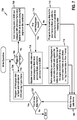
- FIG. 1 illustrates an exemplary configuration of a system with a flash controller coupled to a flash storage device and a host device, where the flash controller is configured to perform fast flash programming of a sequence of image frames or other input data stream.
- FIG. 2 illustrates an exemplary frame of a sequence of image frames for processing by the flash controller of FIG. 1 , and particularly illustrating individual page-sized frame segments of the exemplary frame for storage in a NAND memory device.
- FIG. 3 illustrates exemplary previous and current frames of a sequence of image frames for processing by the flash controller of FIG. 1 , and particularly illustrating matching frame segments within the previous and current frames.
- FIG. 4 illustrates exemplary previous and current frames of a sequence of image frames for processing by the flash controller of FIG. 1 , and particularly illustrating a segment of the current frame, its corresponding segment in the previous frame, and the neighboring frames to that corresponding segment.
- FIG. 5 illustrates exemplary write operations for use with the flash controller of FIG. 1 .
- FIG. 6 illustrates exemplary read operations for use with the flash controller of FIG. 1 .
- FIG. 7 further illustrates exemplary write operations for use with the flash controller of FIG. 1 .
- FIG. 8 further illustrates exemplary read operations for use with the flash controller of FIG. 1 .
- FIG. 9 illustrates exemplary erase operations for use with the flash controller of FIG. 1 .
- FIG. 10 summarizes features of an exemplary memory controller.
- FIG. 11 summarizes exemplary operations for use with the memory controller of FIG. 10 to store recordings.
- FIG. 12 further summarizes exemplary operations for use with the memory controller of FIG. 10 to store recordings or other data streams.
- FIG. 13 summarizes exemplary operations for use with the memory controller of FIG. 10 to read recordings or other data streams.
- FIG. 14 further summarizes exemplary operations for use with the memory controller of FIG. 10 to store recordings or other data streams.
- Flash fast program mode for solid state device (SSD) flash drives or other drives employing non-volatile memory (NVM), or for use with other storage devices.
- SSD solid state device
- NVM non-volatile memory
- adjacent video frames contain a considerable amount of the same information, especially at high FPS video rates. Therefore, adjacent frames may have much of the same data to be written to the flash array between two consecutive frames.
- the flash controller temporarily holds the data of the previous frame in random access memory (RAM) and then compares the data of the current and previous frames.
- RAM random access memory
- the comparison may be on a page-by-page basis with the firmware of the flash controller comparing the data of two pages corresponding to the same X-Y location within the previous and current frames. If two pages contain identical data, the flash controller creates a link between the two pages to enable a single reference to the linked page that corresponds with the previous frame. That is, the flash drive need not store pages of the current frame that match pages already stored for the previous frame. This may allow faster storage rates to accommodate high frame rate recordings (i.e. high frame rate data streams) and may also help extend the lifespan of the memory device, since the memory device need not store as much data as compared to systems that would separately store all pages for all frames.
- the firmware of the flash controller uses the stored links to identify the storage locations (e.g. physical memory addresses) of any matching portions of a frame stored in connection with a previous frame so each complete frame may be reconstructed from the stored pages of data.
- the host device e.g., smartphone, video camera, etc.
- the flash drive may determine which groups of data belong to the same frame.
- the flash controller programs all the data to its NAND array and the data remains in the RAM even when the program operation is finished.
- the first frame then becomes the previous frame, and the flash controller performs a comparison of the data of the current frame and the previous frame that remains in the RAM.
- the compare operation may be enabled through an exclusive-or (XOR) engine or XOR component of the flash controller, which may begin to run as soon as two frames of data are available.
- XOR exclusive-or
- a segment e.g. a portion of the frame the size of a NAND page
- a link is established by the flash controller between the two pages.
- the flash controller performs a flash write operation only for one of the linked pages and, once the operation has completed, the firmware releases the data in the RAM for both of the linked pages.
- a link is maintained in a linking table (which may also be referred to as a control table or a mapping table) for all the pages that are linked together (i.e. adjacent frames that have at least one matching page), the total number of pages written to the flash memory may be minimized. The overall flash write time can thus be improved.
- firmware on the flash drive may be notified (or otherwise made aware) of the frame size from the host device so the flash controller can process the data corresponding to each input frame separately to compare it with the next input frame on demand during runtime.
- the flash fast program mode may be employed with high resolution (HR) burst mode photography and with other streams of input data where separate frames may include matching data, such as with high speed logic analyzers.
- flash write speeds may be increased significantly for HD video recordings, HR burst mode photography, and other applications without requiring any major changes to flash controller hardware specifications.
- the total recorded size of the video or burst mode images may be reduced without sacrificing image quality while improving the total recording time of the images.
- the techniques described herein may be advantageous whenever memory write speed is a bottleneck and the data to be stored contains significant portions of identical information. That is, at least some of the techniques described herein may apply to processing any data stream that involves large amounts of data to be stored over a short time period or short duration, where the data has substantial similarity that can be exploited.
- FIG. 1 illustrates, at a high level, a flash memory storage system 100 that receives data for storage from a host device 102 (such as HD video from an HD video camera or HR burst mode images from a HR camera).
- a flash controller 104 includes a processor 106 with a frame segment comparator 108 , such as XOR engine.
- the flash controller 104 also includes a RAM 110 with temporary frame storage 112 for temporarily storing consecutive frames on input data to identify any matching segments (e.g. pages) so that the aforementioned links may be generated between matching segments.
- the RAM 110 may also include temporary link storage 113 for storing the links during run-time processing.
- the flash storage 114 includes a frame segment storage portion 118 for storing the segments (e.g. pages) of various frames and a frame segment link (mapping) table 120 for storing the links between the segments.
- the linking table may be initially generated in RAM, then transferred to the NAND so that the flash controller can access the links following a subsequent power-up.
- Data is initially received by the flash controller 104 from the host device 102 along an external bus 122 , which may also output data to the host device 102 .
- the frame is stored in temporary frame storage 112 along with the previous frame.
- the processor 106 applies the latest (current) frame and the previous (last) frame to the frame segment comparator 108 to compare the frames and identify matching segments (e.g. identical pages).
- the details of the procedure which may include comparing pages of the current frame against both a corresponding page of the previous frame and adjacent pages to that corresponding page of the previous frame, will be described below. Whenever a match is found that permits a segment of the current frame to be omitted (or excluded) during storage of the current frame, a suitable link is generated by the processor 106 .
- All segments of the current frame that were not found to match a segment of the previous frame (and hence need to be stored) are then transferred to the flash storage 114 for storage in frame segment storage 118 . Any segments of the current frame that were found to match a segment of the previous frame (and hence need not be stored) are not transferred to the flash storage 114 . Rather, only the corresponding link is sent to the flash storage 114 for storage with other links in the frame segment link table (mapping) 120 .
- the procedure may be reversed.
- the segments of the first frame of an image sequence are retrieved by the flash controller 104 from the frame segment storage 118 along bus 116 for output to the host device 102 that originally provided the images or to a separate display device (not shown).
- the second frame all segments stored for that frame are retrieved from the frame segment storage 118 along with any matching segments from the first frame (located using the links within the frame segment link table 120 ).
- the processor reconstructs the complete second frame by combining the various segments together for output to the host device 102 .
- Each additional frame is then processed in a similar manner
- links within the frame segment link table 120 might link segments from that frame to a segment originally stored only in connection with the first frame (e.g. if a particular image segment remains unchanged in the three consecutive frames). Nevertheless, the processor then reconstructs the complete third frame by combining its various segments together for output to the host device 102 .
- a host device (such as a smartphone) may therefore capture images at higher FPS and resolution.
- the flash controller 104 of FIG. 1 may be physically located or installed within the host device 102 .
- the flash controller 104 may be incorporated on the same die. This technique is used, for example, in Open Multimedia Applications Platform (OMAP) processors.
- OMAP Open Multimedia Applications Platform
- the flash controller 104 may be configured as a separate physical element coupled between the host processor 102 and the NAND 114 .
- This architecture is used, e.g., in portable Universal Serial Bus (USB) Flash Drives (UFDs), where the flash controller 104 may be packaged inside the UFD and interacts, on one side, using a device-side interface with the NAND 114 and also interacts, on the other side, with a processor of the host device 102 using a host-side interface (e.g., USB interface with USB protocol).
- USB Universal Serial Bus
- the host 102 may interact with the flash controller 104 using a standard protocol such as USB or Advanced Technology Attachment (ATA), as the interaction is external to the host processor, it is thus more convenient to use standard protocols that are already supported by the processor for other purposes.
- USB Universal Serial Bus
- ATA Advanced Technology Attachment
- the flash controller 104 may be physically located within the NAND 114 as a component thereof. See, for example, mobile disk on chip (mDOC) storages devices.
- the host 102 may interact with the flash controller 104 using either a standard protocol such as USB or a semi-standard protocol as is the case in the mDOC.
- mDOC mobile disk on chip
- features of the flash fast program mode described herein may be implemented in any of a variety of different flash system architectures and within non-flash storage devices as well.
- FIG. 2 illustrates an exemplary frame 200 from a video image, where the frame is subdivided into segments 202 , each corresponding to one page of a NAND storage device.
- the granularity of programming on the NAND is a word line (WL) or page, which is 8 (kilobyte) KB/16 KB for a single level cell (SLC).
- WL word line
- SLC single level cell
- the file size is often about 20 MB (megabyte).
- storage of the HR video might require more than two thousand SLC pages to store the image of the corresponding size.
- Even with a compression algorithm such as JPEG where the image size may be reduced by 90%, storage might still require more than two hundred SLC pages to store the video.
- each SLC page stores only a small portion of the whole image.
- the time interval of the adjacent frames is often less than 40 ms at 30 fps. Therefore, two adjacent frames often contain many pages of identical data that can be linked together and programmed to flash as a single entity.
- FIG. 3 illustrates an exemplary previous frame 300 and a current frame 302 that have several identical 8 KB page sections or segments.
- the identical (matching) segments are tinted gray in the figure and include, for example, segment 304 of frame 300 and identical segment 306 of frame 302 .
- Non-identical (non-matching) segments include, for example, segment 308 of frame 300 and segment 310 of frame 302 .
- the portions of the frames that correspond to the sky, the building and the foreground street match from one frame to the next since these portions of the frames are static.
- the portions of the frames that correspond to trees and shrubbery differ subtly from one frame to the next due to, for example, a breeze that may rustle the leaves of the trees and shrubbery.
- the flash fast program mode described herein takes advantage of matching segments by creating links between pages containing the same data instead of programming all such pages. This may be described as exploiting a “partial-identical” property of consecutive frames, i.e. some portions of consecutive frames are identical (although other portions are not).
- FIG. 4 illustrates that each page segment of a frame may be compared with the page segment at the same location in the previous frame and its adjacent (or neighboring) segments. That is, FIG. 4 shows a first (previous) frame 400 and a second (current) frame 402 . An exemplary segment N in the current frame is highlighted (segment 404 ) along with the corresponding segment N of the previous frame (segment 406 ) and its eight adjacent or neighboring segments 408 , which are above, below, or diametrically adjacent to segment 406 .
- All the segments of a particular frame may be labeled by the firmware of the flash drive based on their location in the frame.
- the flash controller scans the segments one by one. For Segment N 404 in the current frame 402 , the flash controller performs a XOR comparison on the corresponding Segment N 406 in the previous frame 400 . If the XOR does not detect or identify an identical match (i.e. the flash drive does not detect the identicalness of the two segments N that are compared), the flash controller continues by then comparing the current segment N 404 with the segments 408 surrounding the segment N 406 in the previous frame 400 . If the flash controller detects a match (i.e.
- a link between the matching segments is created. If the flash controller does not find or detect a match in segment 406 and any of segments 408 , the flash controller programs the data of segment N 404 into the NAND array. This procedure may be performed by, e.g., beginning at the top left corner of an image frame and proceeding sequentially left to right, row by row, until reaching the bottom right corner of the frame. Each segment N of the current frame is thereby sequentially compared against corresponding segments of the previous frame and its adjacent segments.
- the flash controller flushes the data of the previous frame while maintaining the data of the current frame so the flash controller may then perform the same XOR comparison on the next (new) frame in RAM.
- a XOR is employed in the exemplary embodiments described herein, other comparison devices or procedures may be used to detect matching segments.
- the flash controller may be configured to instead detect a substantial match, i.e.
- the flash drive determines whether nearly all of the bits of one segment match those of the comparison segment (based on some predetermined threshold of similarity such as if at least 99.9% of the bits match).
- XOR's are used in the embodiments described in detail herein because a XOR is particularly efficient, and flash drives often already include XOR engines that may be easily exploited for the page comparison purposes described herein.
- FIG. 5 illustrates an exemplary write procedure 500 for use by a flash drive controller to perform the “flash fast program mode” procedure.
- the flash controller inputs a sequence of consecutive frames from an HD Video Camera, HR Burst Mode Camera or other device, and stores a first frame of the sequence in physical memory.
- the flash drive controller temporarily stores each pair of consecutive frames in RAM (i.e. a current frame and the previous frame).
- the flash controller sequentially compares each page-sized segment (N) of the current frame with a corresponding page-sized segment (N) of the previous frame and with each of the eight adjacent page-sized segments (N adj ) of the corresponding segment (N) within the previous frame.
- the flash controller identifies each segment (N) of the current frame that matches either the corresponding segment (N) of the previous frame or any of its eight adjacent segments (N adj ).
- the flash controller For each segment (N) of the current frame that is found to match a segment of the previous frame, the flash controller generates and stores a link in memory lookup table (LUT) that links the segment (N) of the current frame with the physical memory location (e.g. address) of the matching frame of the previous frame, so that the matching segment of the current frame need not be separately stored in physical memory.
- the flash controller separately stores all other segments (N) of the current frame within the physical NAND memory (i.e.
- Processing may then return to block 504 to process a next frame. The procedure may be repeated until all frames of an input recording or other input data stream are processed and stored in the NAND memory.
- FIG. 6 illustrates an exemplary read procedure 600 for use by a flash controller to read data previously stored using the flash fast procedure.
- the flash controller reads all page-sized segments of the first frame of a stored sequence of image frames from physical NAND memory by accessing the lookup linking table that links each segment to its physical memory location or address.
- the flash controller reads all segments of a particular frame by following links in the lookup table to corresponding physical memory addresses, and then combines or merges the segments into a frame, including any matching segments originally stored for a predecessor frame and any unique segments that had been stored separately for the particular frame.
- the flash drive controller outputs the sequence of frames, including any frames that have been “reconstructed” from separately stored segments, to the host device for display thereon or to another device.
- TABLE I illustrates an exemplary linking table (or mapping or control table) that includes the mapping or linking indexes or indices for tracking the logical block addresses (LBAs) that are written to corresponding NAND physical locations or addresses by the flash drive.
- LBAs logical block addresses
- the linking table stores row values for the following column values: “Index,” “LBA,” “Physical Block Location,” “Linked Index,” and “Segment of Frame.”
- the Index is a value that is sequentially assigned by the flash controller to track LBA's and their memory locations or addresses. The purpose of the Index is to tag each entry in the table in a sequential order. Each Index value corresponds to a different range of LBA's.
- the index row lists the corresponding Physical Block Location within the flash (NAND) memory and the corresponding segment of data (e.g. a page or segment N of a frame M of a HD video) but does not include a Linked Index.
- the index row instead lists or records the corresponding Link Index.
- LBAs (0-700) correspond to segment-A of a previous frame and segment-A is programmed to the NAND flash memory but the data is still held in a double-data rate (DDR) memory of the flash device.
- LBAs (701-1400) correspond to segment-B of a current frame held in DDR, which exactly matches segment-A already programmed to the NAND on Physical Block Locations ‘A’ through ‘A+6’.
- the flash controller firmware then will not program the segment B to the NAND.
- LBAs (701-1400) are not programmed to the NAND but are instead linked to LBAs (0-700) that correspond to segment A. These LBAs are indexed in the table as 0 through 6. The indexes (0 ⁇ 6) are used in the Linked Index column for LBAs (701 ⁇ 1400) to indicate that the data in these particular LBAs is exactly the same as in LBAs (0 ⁇ 700).
- the flash controller firmware checks the Linked Index column to detect or confirm the presence of any entry in that column. If an entry is found, the flash controller firmware reads the index corresponding to the LBA read and accesses the table again to find the Index and the corresponding Physical Location on the NAND memory to read the data. For example, if a host requests data from LBA-1150, the flash controller firmware reads the Linked Index column and finds an entry ‘4’. The flash controller firmware then reads the row with Index-4 and obtains the Physical Address ‘A+4’ and services the read command from this location.
- the flash controller firmware When an erase operation to delete an image is requested by a host, the flash controller firmware makes sure there are no linked indexes to the pages that correspond to the image for which an erase operation is requested. For example, if an image corresponding to LBAs (0-100) is requested to be deleted (erased) by the host device, the flash controller firmware checks the Linked Indexes to detect or confirm the presence of any linked indexes that correspond to the same Index value. In the example of TABLE I, LBAs-701-800 are linked to the LBAs 0-100 through Linked Index 0. Therefore, even though LBAs 0-100 are released and dereferenced by the flash controller firmware, the physical location or address is not erased.
- the flash controller firmware instead of erasing the Physical Block Location, the flash controller firmware instead dereferences LBA 0-100 and maps the Physical Block Location to LBA 701-800. Once the operation is complete, the index 0 is released for later use.
- TABLE II illustrates a portion of a linking table that has been updated to reflect completion of an erase operation, as just described.
- FIG. 7 illustrates details of an exemplary write procedure or operation 700 for use by a flash drive controller, which may exploit TABLE I or other suitable linking or mapping tables.
- the write procedure begins sometime following a system startup or power-up, where the flash controller is already configured or programmed with the known frame size of the data to be processed.
- the flash controller then waits for a new data frame, at block 705 , and, once a new data frame is found, at decision block 707 , processing proceeds to block 708 via decision block 704 where the new data is processed (e.g. the data of a next frame).
- the flash controller holds incoming data in DDR and compares the data with the previous frame also held in DDR on an 8 k basis using the XOR engine on the controller. If no matching pages are found or detected, at decision block 710 , the flash controller programs the incoming data, at processing block 712 , in the new frame to flash as with the previous frame and updates the mapping table. The flash controller again waits for a new data frame, at 705 , and, once another new data frame is found, at decision block 707 , processing again proceeds to block 708 (via decision block 704 ) where the new data is processed (e.g. the data of the next frame).
- the flash controller updates the linked index with the index of stored pages in flash from the previous frame, and retires previous frame in DDR. Then, at processing block 716 , the flash controller retires the remaining non-matching pages in the current data to flash and updates the index in the mapping table, and then tags all the pages stored in the DDR in the current data frame as prev.frame.
- the flash controller again waits for a new data frame, at block 705 , and, if no new data frame is found, at decision block 707 , the write procedure is complete (i.e. END). Otherwise, processing continues as already described for the next frame.
- FIG. 8 illustrates details of an exemplary read procedure or operation 800 for use by a flash controller to read a page of data stored using the write procedure of FIG. 7 .
- the exemplary read procedure begins sometime following system startup or power-up, with the flash controller knowing the frame size.
- the flash controller checks the linking table to locate the LBA in NAND for the page to be read and to detect or confirm the presence of a linked index in the table for that page. Assuming a linked index is found in the table (via decision block 806 ), the flash controller then determines whether a physical mapping address is also found for that page (via a decision block 808 ) for the data.
- the flash controller reads the physical location of the page corresponding to the linked index from the table and toggles out the page of data from the memory device (by accessing that particular physical memory location).
- processing instead proceeds to block 812 where the flash controller reports to the host device that the LBA is not mapped on the flash drive (e.g. an error is reported to indicate that the LBA identified at 804 does not correspond to a known physical memory address).
- processing proceeds to block 814 where the flash controller reads the page data from memory corresponding to the physical location and toggles out the data that has been read. The read operation for that page is then complete (i.e. END).
- the procedure is then repeated for the next page of data within a current frame, and then for the pages of subsequent frames until all frames are read.
- FIG. 9 illustrates further details of an exemplary erase procedure or operation 900 for use by a flash drive controller to erase a page of data stored using the procedure of FIG. 7 .
- the exemplary erase procedure begins with the flash controller already knowing the frame size.
- the flash controller determines whether the block (e.g. frame) to erase has any pages with a linked index in the linking table. If so, then, at 906 , since the page is linked to another page, the flash controller does not erase the block because a linked index page may refer to this block during read operation. Assuming, however, that the determination at 904 is NO, then, at 908 , the flash controller determines whether the index of the page to erase is present in the linked index column of the table.
- the block e.g. frame
- the flash controller removes the linked index entry in the linking (mapping) table. Otherwise, at 912 , since there is no linked index corresponding to the page, the block containing the page can be erased and the linking (mapping) table is updated accordingly by the flash controller by releasing the index corresponding to the page. (That is, in this example, the granularity of the erase operation is for a block, rather than a page, although in other implementations a different erase granularity might be used.) Although not shown, the erase procedure may then be repeated for the next page or block of data within a current frame, and then for other frames that need to be erased.
- FIGS. 10-13 illustrate and summarize various general features of exemplary memory controllers and methods or procedures for use with memory controllers.
- FIG. 10 shows an exemplary memory controller 1000 configured to communicate with a memory device 1002 .
- the memory controller 1000 may operate in conjunction with a host device, such as a video camera, smartphone or the like, which provides an input recording or other input data stream consisting of sequential frames (e.g. HD video or HR burst mode images).
- a host device such as a video camera, smartphone or the like
- the memory device may be any suitable storage device and is not limited to NANDs
- the memory controller may be any suitable memory control device or memory access device and is not limited to flash controllers.
- the exemplary memory controller 1000 of FIG. 10 includes a processor 1004 for controlling storage, retrieval and/or erasure of data within the memory device 1002 .
- the exemplary processor 1004 includes a comparison component 1006 (e.g. a comparator such as a XOR engine) configured to compare, at least, first and second frames of an input recording or other input data stream to identify a matching portion and a storage (write) controller 1008 configured to store, at least, the first frame at first physical locations or addresses within the memory device while including the matching portion, and to store the second frame at second physical locations or addresses within the memory device while excluding the matching portion.
- the frames may be stored in a frame storage portion 1010 of the memory device 1002 that includes first physical memory locations or addresses and second physical memory locations or addresses.
- a link storage controller 1012 is configured to store, at least, a link between the second frame and the matching portion of the first frame to permit the second frame to be “reconstructed” in a subsequent read operation, where the link may be stored in a link storage portion 1014 of the memory device 1002 .
- the link may link or map a logical memory address of the matching portion of the second frame with a physical memory address of the matching portion of the first frame.
- An access controller 1016 of the processor 1004 is configured to access the memory device 1002 to initiate storage retrieval when one or more frames of the recording or other input data stream needs to be accessed (typically in response to a request from a host).
- a storage (read) controller 1018 is configured to read, at least, the first frame and the second frame from the memory device 1002 while obtaining the matching portion stored along with the first frame.
- a combining component (e.g. a combiner) 1020 may be configured to combine the matching portion obtained from first frame with non-matching portions of the second frame to permit reconstruction of the entire second frame, either by the memory controller or a host device receiving the read data.
- the memory controller 1000 of FIG. 10 may sequentially process millions of frames of a recording or other input data stream.
- an apparatus e.g. processor 1004
- a storage device e.g. memory device 1002
- the apparatus includes: means for comparing first and second frames of an input recording or other input data stream to identify a matching portion (such as comparator 1006 ); means for storing the first frame at first physical locations or addresses within the memory device while including the matching portion and for storing the second frame at second physical locations or addresses within the memory device while excluding the matching portion (such as storage controller 1008 ); means for storing a link between the second frame and the matching portion of the first frame (such as link storage 1014 ); and means for reading the second frame from the memory device while using the link to obtain the matching portion that was excluded during storage of the second frame but was included during storage of the first frame (such as read controller 1018 ).
- the apparatus may additionally, or alternatively, include: means for accessing a memory device in which a recording or other input data stream is stored having first and second frames, where a portion of the second frame that matches a matching portion of the first frame is stored along with the first frame at first physical memory locations or addresses and wherein non-matching portions of the second frame are stored at second physical memory locations or addresses (such as access controller 1016 ); means for reading the first frame of the recording or other input data stream from the first physical addresses of the memory device and for reading the second frame of the recording or other input data stream from the memory device by obtaining the non-matching portions from the second physical addresses and obtaining the matching portion stored along with the first frame from the first physical addresses (such as read controller 1018 ); and means for combining the matching portion obtained from first frame with the non-matching portions of the second frame to reconstruct the second frame (such as combiner 1020 ).
- the frames may be stored in a means for storing frames (such as storage portion 1010 ).
- a means for storing a link between the second frame and the matching portion of the first frame may be provided (such as link storage 1014 ) where the link serves to link or map a physical address of the matching portion of the first frame to a logical address of the matching portion of the second frame.
- a machine-readable storage medium may be provided having one or more instructions which when executed by a processing circuit causes the processing circuit to performing the functions illustrated in FIG. 10 and/or other functions illustrated or described herein.
- instructions may be provided for: comparing first and second frames of an input recording or other input data stream to identify a matching portion; storing the first frame at first physical locations or addresses within the memory device while including the matching portion; storing the second frame at second physical locations or addresses within the memory device while excluding the matching portion; storing a link between the second frame and the matching portion of the first frame; and reading the second frame from the memory device while using the link to obtain the matching portion that was excluded during storage of the second frame but was included during storage of the first frame.
- the instructions may additionally, or alternatively, include instructions for accessing a memory device in which a recording or other input data stream is stored having first and second frames, where a portion of the second frame that matches a matching portion of the first frame is stored along with the first frame at first physical memory locations or addresses and wherein non-matching portions of the second frame are stored at second physical memory locations or addresses. Instructions may also be provided for: reading the first frame of the recording or other input data stream from the first physical addresses of the memory device; reading the second frame of the recording or other input data stream from the memory device by obtaining the non-matching portions from the second physical addresses; and obtaining the matching portion stored along with the first frame from the first physical addresses.
- FIG. 11 broadly summarizes exemplary operations 1100 for use with a memory controller or other suitable device to store or otherwise process recordings or other input data streams.
- the memory controller compares first and second frames of an input data stream (e.g. a recording) to identify a matching portion.
- the memory controller stores the first frame at first physical locations or addresses within a memory device (such as a NAND) while including the matching portion.
- the memory controller stores the second frame at second physical locations or addresses within the memory device while excluding the matching portion.
- the memory controller stores a link between the second frame and the matching portion of the first frame.
- the memory controller reads the first frame and the second frame from the memory device while using the link to obtain the matching portion that was excluded during storage of the second frame but was included during storage of the first frame to allow the matching portion stored with the first frame to be combined with the other portions of the second frame to reconstruct the entire second frame (where the “reconstruction” of the entire second frame might be done by the memory controller or by a host device).
- FIG. 12 further summarizes exemplary operations 1200 for use with a memory controller to store or otherwise process recordings or other input data streams.
- the memory controller compares first and second frames of an input recording to identify a matching portion, where the first and second frames are consecutive frames of a video recording or consecutive frames of burst-mode photographic images, and where the matching portion is identified by comparing a segment N of the second frame with a corresponding segment N of the first frame or with any segments M of the first frame that are adjacent to the segment N of the first frame to detect an identical match (or, alternatively, a substantial match).
- the memory controller stores the first frame at first physical locations or addresses with a NAND while including the matching portion by storing each segment N of the first frame at the first physical memory locations or addresses.
- the memory controller stores the second frame at second physical locations or addresses with the NAND while excluding the matching portion by storing each segment M of the second frame that does not match any segment N of the first frame, and then repeat the process for additional frames.
- the memory controller stores a link between the second frame and the matching portion of the first frame by generating an index that links a logical address of the portion of the second frame that is not stored with a physical address of the matching portion of the first frame that is stored, and then repeats the process for additional frames.
- the memory controller reads the entire first frame of the recording from the memory device from the first physical addresses and then reads the second frame while using the link to obtain the matching portion stored among the first physical addresses that was excluded during storage of the second frame (from the second physical addresses) but included during storage of the first frame).
- the memory controller may combine the matching portion obtained from first frame with non-matching portions of the second frame read from the memory device to reconstruct the second frame, and the repeats the operations for additional frames. In other examples, the memory controller merely outputs the read data to an external host that may then combine the various portions of the second frame together.
- FIG. 13 summarizes exemplary operations 1300 for use with a memory controller to read or otherwise process recordings or other data streams.
- the memory controller accesses a memory device in which a data stream (e.g. a recording) is stored having first and second frames, where at least a portion of the second frame that matches a matching portion of the first frame is stored along with the first frame.
- the memory controller reads the first frame of the data stream from the memory device.
- the memory controller reads the second frame of the recording from the memory device while obtaining the matching portion stored along with the first frame.
- the memory controller combines the matching portion obtained from first frame with non-matching portions of the second frame read from the memory device to reconstruct the second frame.
- FIG. 14 further summarizes exemplary operations 1400 for use with a memory controller to read or otherwise process recordings or other data streams.
- the memory controller accesses a memory device in which a recording or other data stream is stored having first and second frames, where a matching portion of the second frame that matches a portion of the first frame is stored at first physical addresses along with the first frame but not at second physical addresses along with the second frame, and where the first and second frames are consecutive frames of a video recording or consecutive frames of burst-mode photographic images, and where the matching portion is a segment N of the second frame that identically (or substantially) matches a corresponding segment N of the first frame or identically (or substantially) matches any segments M of the first frame that are adjacent to segment N of the first frame.
- the memory controller reads the entire first frame of the recording from the first physical addresses of the memory device by reading each segment N of the first frame.
- the memory controller reads the second frame of the recording from the memory device while obtaining the matching portion stored along with the first frame by reading each segment of the second frame that is stored at the second physical addresses for the second frame and reading any matching portion N that was stored along with the first frame at the first physical addresses by accessing an index that links a logical address of the matching portion of the second frame to the first frame.
- the memory controller may combine the matching portion obtained from the first physical addresses of the first frame with the other (non-matching) portions of the second frame read from the second physical addresses to reconstruct the second frame, and repeats the process for additional frames.
Landscapes
- Engineering & Computer Science (AREA)
- Theoretical Computer Science (AREA)
- Physics & Mathematics (AREA)
- General Engineering & Computer Science (AREA)
- General Physics & Mathematics (AREA)
- Multimedia (AREA)
- Signal Processing (AREA)
- Computing Systems (AREA)
- Techniques For Improving Reliability Of Storages (AREA)
Abstract
Description
| TABLE I | ||||
| Physical | ||||
| Block | Linked | |||
| Index | LBA | Location | Index | Segment of Frame |
| 0 | 0-100 | A | — | Segment N in frame M |
| 1 | 101-200 | A + 1 | — | Segment N + 1 in frame M |
| 2 | 201-300 | A + 2 | — | Segment N + 2 in frame M |
| 3 | 301-400 | A + 3 | — | Segment N + 3 in frame M |
| 4 | 401-500 | A + 4 | — | Segment N + 4 in frame M |
| 5 | 501-600 | A + 5 | — | Segment N + 5 in frame M |
| 6 | 601-700 | A + 6 | — | Segment N + 6 in frame M |
| 7 | 701-800 | — | 0 | Segment N in frame M + 1 |
| 8 | 801-900 | — | 1 | Segment N + 1 in frame M + 1 |
| 9 | 901-1000 | — | 2 | Segment N + 2 in frame M + 1 |
| 10 | 1001-1100 | — | 3 | Segment N + 3 in frame M + 1 |
| 11 | 1101-1200 | — | 4 | Segment N + 4 in frame M + 1 |
| 12 | 1201-1300 | — | 5 | Segment N + 5 in frame M + 1 |
| 13 | 1301-1400 | — | 6 | Segment N + 6 in frame M + 1 |
| TABLE II | ||||||
| Physical | ||||||
| block | Linked | |||||
| Index | LBA | location | Index | Segment of Frame | ||
| — | 0-100 | — | |||
| 7 | 701-800 | A | |||
Claims (21)
Priority Applications (1)
| Application Number | Priority Date | Filing Date | Title |
|---|---|---|---|
| US15/890,118 US10747659B2 (en) | 2018-02-06 | 2018-02-06 | Flash fast program mode for high definition video recording and high resolution camera burst mode recording |
Applications Claiming Priority (1)
| Application Number | Priority Date | Filing Date | Title |
|---|---|---|---|
| US15/890,118 US10747659B2 (en) | 2018-02-06 | 2018-02-06 | Flash fast program mode for high definition video recording and high resolution camera burst mode recording |
Publications (2)
| Publication Number | Publication Date |
|---|---|
| US20190243754A1 US20190243754A1 (en) | 2019-08-08 |
| US10747659B2 true US10747659B2 (en) | 2020-08-18 |
Family
ID=67475118
Family Applications (1)
| Application Number | Title | Priority Date | Filing Date |
|---|---|---|---|
| US15/890,118 Active 2038-05-11 US10747659B2 (en) | 2018-02-06 | 2018-02-06 | Flash fast program mode for high definition video recording and high resolution camera burst mode recording |
Country Status (1)
| Country | Link |
|---|---|
| US (1) | US10747659B2 (en) |
Families Citing this family (7)
| Publication number | Priority date | Publication date | Assignee | Title |
|---|---|---|---|---|
| US10897627B2 (en) | 2019-01-11 | 2021-01-19 | Western Digital Technologies, Inc. | Non-volatile memory system including a partial decoder and event detector for video streams |
| US11064194B2 (en) | 2019-10-31 | 2021-07-13 | Western Digital Technologies, Inc. | Encoding digital videos using controllers of data storage devices |
| US10841645B1 (en) | 2019-12-09 | 2020-11-17 | Western Digital Technologies, Inc. | Storage system and method for video frame segregation to optimize storage |
| US11562018B2 (en) | 2020-02-04 | 2023-01-24 | Western Digital Technologies, Inc. | Storage system and method for optimized surveillance search |
| US11328511B2 (en) | 2020-03-13 | 2022-05-10 | Western Digital Technologies, Inc. | Storage system and method for improved playback analysis |
| US12079511B2 (en) * | 2020-12-26 | 2024-09-03 | SanDisk Technologies, Inc. | Devices and methods for optimized fetching of multilingual content in media streaming |
| US11908523B2 (en) * | 2021-09-01 | 2024-02-20 | Micron Technology, Inc. | Express programming using advanced cache register release in a memory sub-system |
Citations (14)
| Publication number | Priority date | Publication date | Assignee | Title |
|---|---|---|---|---|
| US20020081090A1 (en) | 2000-12-22 | 2002-06-27 | Philips Electronics North America | System and method for determining whether a video program has been previously recorded |
| US20040008779A1 (en) * | 2002-06-18 | 2004-01-15 | Lai King Chung | Techniques for video encoding and decoding |
| US20050163220A1 (en) * | 2004-01-26 | 2005-07-28 | Kentaro Takakura | Motion vector detection device and moving picture camera |
| CN1933575A (en) | 2006-09-30 | 2007-03-21 | 康佳集团股份有限公司 | Video recording method for photographic hand-held equipment |
| US7433994B2 (en) | 2004-12-07 | 2008-10-07 | Ocz Technology Group, Inc. | On-device data compression to increase speed and capacity of flash memory-based mass storage devices |
| US20090043948A1 (en) | 2005-04-15 | 2009-02-12 | Thomson Licensing Llc | Method and System for Storing Logical Data Blocks Into Flash-Blocks in Multiple Non-Volatile Memories Which Are Connected to At Least One Common Data I/0 Bus |
| US20110060887A1 (en) * | 2009-09-09 | 2011-03-10 | Fusion-io, Inc | Apparatus, system, and method for allocating storage |
| US20120106852A1 (en) * | 2010-10-28 | 2012-05-03 | Microsoft Corporation | Burst mode image compression and decompression |
| US20140281361A1 (en) * | 2013-03-15 | 2014-09-18 | Samsung Electronics Co., Ltd. | Nonvolatile memory device and related deduplication method |
| CN204291206U (en) | 2014-12-30 | 2015-04-22 | 西安奇维科技股份有限公司 | A kind of HD video data logger based on flash array |
| JP2015080149A (en) | 2013-10-18 | 2015-04-23 | 日本放送協会 | Video recording device and video recording method |
| US20150199138A1 (en) | 2014-01-14 | 2015-07-16 | Georgia Tech Research Corporation | Multi-tiered storage systems and methods for adaptive content streaming |
| US20150294187A1 (en) * | 2014-04-14 | 2015-10-15 | Canon Kabushiki Kaisha | Image search apparatus and control method thereof |
| CN106101596A (en) | 2016-08-15 | 2016-11-09 | Tcl集团股份有限公司 | A kind of video storage method and device |
-
2018
- 2018-02-06 US US15/890,118 patent/US10747659B2/en active Active
Patent Citations (14)
| Publication number | Priority date | Publication date | Assignee | Title |
|---|---|---|---|---|
| US20020081090A1 (en) | 2000-12-22 | 2002-06-27 | Philips Electronics North America | System and method for determining whether a video program has been previously recorded |
| US20040008779A1 (en) * | 2002-06-18 | 2004-01-15 | Lai King Chung | Techniques for video encoding and decoding |
| US20050163220A1 (en) * | 2004-01-26 | 2005-07-28 | Kentaro Takakura | Motion vector detection device and moving picture camera |
| US7433994B2 (en) | 2004-12-07 | 2008-10-07 | Ocz Technology Group, Inc. | On-device data compression to increase speed and capacity of flash memory-based mass storage devices |
| US20090043948A1 (en) | 2005-04-15 | 2009-02-12 | Thomson Licensing Llc | Method and System for Storing Logical Data Blocks Into Flash-Blocks in Multiple Non-Volatile Memories Which Are Connected to At Least One Common Data I/0 Bus |
| CN1933575A (en) | 2006-09-30 | 2007-03-21 | 康佳集团股份有限公司 | Video recording method for photographic hand-held equipment |
| US20110060887A1 (en) * | 2009-09-09 | 2011-03-10 | Fusion-io, Inc | Apparatus, system, and method for allocating storage |
| US20120106852A1 (en) * | 2010-10-28 | 2012-05-03 | Microsoft Corporation | Burst mode image compression and decompression |
| US20140281361A1 (en) * | 2013-03-15 | 2014-09-18 | Samsung Electronics Co., Ltd. | Nonvolatile memory device and related deduplication method |
| JP2015080149A (en) | 2013-10-18 | 2015-04-23 | 日本放送協会 | Video recording device and video recording method |
| US20150199138A1 (en) | 2014-01-14 | 2015-07-16 | Georgia Tech Research Corporation | Multi-tiered storage systems and methods for adaptive content streaming |
| US20150294187A1 (en) * | 2014-04-14 | 2015-10-15 | Canon Kabushiki Kaisha | Image search apparatus and control method thereof |
| CN204291206U (en) | 2014-12-30 | 2015-04-22 | 西安奇维科技股份有限公司 | A kind of HD video data logger based on flash array |
| CN106101596A (en) | 2016-08-15 | 2016-11-09 | Tcl集团股份有限公司 | A kind of video storage method and device |
Non-Patent Citations (7)
| Title |
|---|
| Cai, Yu, et al. "Error characterization, mitigation, and recovery in flash-memory-based solid-state drives." Proceedings of the IEEE 105.9 (Aug. 18, 2017): 1666-1704. (Year: 2017). * |
| Chen, Ming, Shupeng Wang, and Liang Tian. "A High-precision Duplicate Image Deduplication Approach." JCP 8.11 (2013): 2768-2775. (Year: 2013). * |
| Dufaux, Frederic, and Fabrice Moscheni. "Motion estimation techniques for digital TV: A review and a new contribution." Proceedings of the IEEE 83.6 (1995): 858-876. (Year: 1995). * |
| Hu, Xiao-Yu, et al. "Write amplification analysis in flash-based solid state drives." Proceedings of SYSTOR 2009: The Israeli Experimental Systems Conference. ACM, 2009. (Year: 2009). * |
| Roodaki-Lavasani, Hoda, and Jani Lainema. "Efficient burst image compression using H. 265/HEVC." Mobile Devices and Multimedia: Enabling Technologies, Algorithms, and Applications 2014. vol. 9030. International Society for Optics and Photonics, 2014. (Year: 2014). * |
| SanDisk, "SanDisk Extreme SD UHS-I Card"; 2017; https://www.sandisk.in/home/memory-cards/sd-cards/extreme-sd-uhs-i; 11 pages. |
| SD Association, "SD Standard for Video Recording"; Date Unknown; https://www.sdcard.org/developers/overview/speed_class/; 4 pages. |
Also Published As
| Publication number | Publication date |
|---|---|
| US20190243754A1 (en) | 2019-08-08 |
Similar Documents
| Publication | Publication Date | Title |
|---|---|---|
| US10747659B2 (en) | Flash fast program mode for high definition video recording and high resolution camera burst mode recording | |
| US10628319B2 (en) | Methods for caching and reading data to be programmed into a storage unit and apparatuses using the same | |
| US8484409B2 (en) | Nonvolatile memory controller with logical defective cluster table | |
| KR101491943B1 (en) | Transaction log recovery | |
| KR102564774B1 (en) | Apparatus for diagnosing memory system or data processing system and operating method of memory system or data processing system based on diagnosis | |
| KR101447786B1 (en) | Power interrupt management | |
| US8996790B1 (en) | System and method for flash memory management | |
| US9703816B2 (en) | Method and system for forward reference logging in a persistent datastore | |
| US9563551B2 (en) | Data storage device and data fetching method for flash memory | |
| US20110035539A1 (en) | Storage device, and memory controller | |
| US10475517B2 (en) | Characterizing and operating a non-volatile memory device | |
| US12045470B2 (en) | Method of writing data in nonvolatile memory device and nonvolatile memory device performing the same | |
| US20110320689A1 (en) | Data Storage Devices and Data Management Methods for Processing Mapping Tables | |
| US20160026408A1 (en) | Storage device metadata synchronization | |
| CN110347613A (en) | Method, controller and the multi-tenant solid-state disk of RAID are realized in multi-tenant solid-state disk | |
| US8819332B2 (en) | Nonvolatile storage device performing periodic error correction during successive page copy operations | |
| US20170285961A1 (en) | 3d stackable hybrid phase change memory with improved endurance and non-volatility | |
| KR102746969B1 (en) | Data storage device and operating method thereof | |
| CN110096452B (en) | Nonvolatile random access memory and method for providing the same | |
| US12505242B2 (en) | Method and non-transitory computer-readable storage medium and apparatus for programming and recovering protected data | |
| US12236116B2 (en) | Systems and methods for selectively controlling programming operations of a memory system comprising a plurality of super blocks | |
| US11782782B2 (en) | Memory system and data processing system | |
| US20240256130A1 (en) | Method of operating storage device using host request bypass and storage device performing the same | |
| US12487768B2 (en) | Storage device managing metadata memory blocks each storing metadata units, and method of operating the same | |
| US12505154B1 (en) | Data storage device and method for video frame link-based management and processing |
Legal Events
| Date | Code | Title | Description |
|---|---|---|---|
| FEPP | Fee payment procedure |
Free format text: ENTITY STATUS SET TO UNDISCOUNTED (ORIGINAL EVENT CODE: BIG.); ENTITY STATUS OF PATENT OWNER: LARGE ENTITY |
|
| AS | Assignment |
Owner name: WESTERN DIGITAL TECHNOLOGIES, INC., CALIFORNIA Free format text: ASSIGNMENT OF ASSIGNORS INTEREST;ASSIGNORS:YU, WEIJIE;SEHGAL, ROHIT;SHEPARD, ZACHARY DAVID;SIGNING DATES FROM 20180202 TO 20180205;REEL/FRAME:044856/0975 |
|
| STPP | Information on status: patent application and granting procedure in general |
Free format text: NON FINAL ACTION MAILED |
|
| STPP | Information on status: patent application and granting procedure in general |
Free format text: RESPONSE TO NON-FINAL OFFICE ACTION ENTERED AND FORWARDED TO EXAMINER |
|
| STPP | Information on status: patent application and granting procedure in general |
Free format text: FINAL REJECTION MAILED |
|
| STPP | Information on status: patent application and granting procedure in general |
Free format text: DOCKETED NEW CASE - READY FOR EXAMINATION |
|
| AS | Assignment |
Owner name: JPMORGAN CHASE BANK, N.A., AS AGENT, ILLINOIS Free format text: SECURITY INTEREST;ASSIGNOR:WESTERN DIGITAL TECHNOLOGIES, INC.;REEL/FRAME:052915/0566 Effective date: 20200113 |
|
| STPP | Information on status: patent application and granting procedure in general |
Free format text: NOTICE OF ALLOWANCE MAILED -- APPLICATION RECEIVED IN OFFICE OF PUBLICATIONS |
|
| STPP | Information on status: patent application and granting procedure in general |
Free format text: AWAITING TC RESP, ISSUE FEE PAYMENT RECEIVED |
|
| STPP | Information on status: patent application and granting procedure in general |
Free format text: PUBLICATIONS -- ISSUE FEE PAYMENT VERIFIED |
|
| STCF | Information on status: patent grant |
Free format text: PATENTED CASE |
|
| AS | Assignment |
Owner name: WESTERN DIGITAL TECHNOLOGIES, INC., CALIFORNIA Free format text: RELEASE OF SECURITY INTEREST AT REEL 052915 FRAME 0566;ASSIGNOR:JPMORGAN CHASE BANK, N.A.;REEL/FRAME:059127/0001 Effective date: 20220203 |
|
| AS | Assignment |
Owner name: JPMORGAN CHASE BANK, N.A., ILLINOIS Free format text: PATENT COLLATERAL AGREEMENT - A&R LOAN AGREEMENT;ASSIGNOR:WESTERN DIGITAL TECHNOLOGIES, INC.;REEL/FRAME:064715/0001 Effective date: 20230818 Owner name: JPMORGAN CHASE BANK, N.A., ILLINOIS Free format text: PATENT COLLATERAL AGREEMENT - DDTL LOAN AGREEMENT;ASSIGNOR:WESTERN DIGITAL TECHNOLOGIES, INC.;REEL/FRAME:067045/0156 Effective date: 20230818 |
|
| FEPP | Fee payment procedure |
Free format text: MAINTENANCE FEE REMINDER MAILED (ORIGINAL EVENT CODE: REM.); ENTITY STATUS OF PATENT OWNER: LARGE ENTITY |
|
| AS | Assignment |
Owner name: SANDISK TECHNOLOGIES, INC., CALIFORNIA Free format text: ASSIGNMENT OF ASSIGNORS INTEREST;ASSIGNOR:WESTERN DIGITAL TECHNOLOGIES, INC.;REEL/FRAME:067567/0682 Effective date: 20240503 Owner name: SANDISK TECHNOLOGIES, INC., CALIFORNIA Free format text: ASSIGNMENT OF ASSIGNOR'S INTEREST;ASSIGNOR:WESTERN DIGITAL TECHNOLOGIES, INC.;REEL/FRAME:067567/0682 Effective date: 20240503 |
|
| AS | Assignment |
Owner name: SANDISK TECHNOLOGIES, INC., CALIFORNIA Free format text: CHANGE OF NAME;ASSIGNOR:SANDISK TECHNOLOGIES, INC.;REEL/FRAME:067982/0032 Effective date: 20240621 |
|
| AS | Assignment |
Owner name: JPMORGAN CHASE BANK, N.A., AS THE AGENT, ILLINOIS Free format text: PATENT COLLATERAL AGREEMENT;ASSIGNOR:SANDISK TECHNOLOGIES, INC.;REEL/FRAME:068762/0494 Effective date: 20240820 |
|
| AS | Assignment |
Owner name: SANDISK TECHNOLOGIES, INC., CALIFORNIA Free format text: PARTIAL RELEASE OF SECURITY INTERESTS;ASSIGNOR:JPMORGAN CHASE BANK, N.A., AS AGENT;REEL/FRAME:071382/0001 Effective date: 20250424 Owner name: JPMORGAN CHASE BANK, N.A., AS COLLATERAL AGENT, ILLINOIS Free format text: SECURITY AGREEMENT;ASSIGNOR:SANDISK TECHNOLOGIES, INC.;REEL/FRAME:071050/0001 Effective date: 20250424 |