US10734541B2 - Method of manufacturing semiconductor device - Google Patents
Method of manufacturing semiconductor device Download PDFInfo
- Publication number
- US10734541B2 US10734541B2 US16/057,858 US201816057858A US10734541B2 US 10734541 B2 US10734541 B2 US 10734541B2 US 201816057858 A US201816057858 A US 201816057858A US 10734541 B2 US10734541 B2 US 10734541B2
- Authority
- US
- United States
- Prior art keywords
- insulating film
- over
- layer
- semiconductor
- type semiconductor
- Prior art date
- Legal status (The legal status is an assumption and is not a legal conclusion. Google has not performed a legal analysis and makes no representation as to the accuracy of the status listed.)
- Active, expires
Links
Images


Classifications
-
- H—ELECTRICITY
- H10—SEMICONDUCTOR DEVICES; ELECTRIC SOLID-STATE DEVICES NOT OTHERWISE PROVIDED FOR
- H10F—INORGANIC SEMICONDUCTOR DEVICES SENSITIVE TO INFRARED RADIATION, LIGHT, ELECTROMAGNETIC RADIATION OF SHORTER WAVELENGTH OR CORPUSCULAR RADIATION
- H10F71/00—Manufacture or treatment of devices covered by this subclass
- H10F71/121—The active layers comprising only Group IV materials
-
- H01L31/1804—
-
- H01L31/02005—
-
- H01L31/02161—
-
- H01L31/028—
-
- H01L31/035281—
-
- H01L31/109—
-
- H—ELECTRICITY
- H10—SEMICONDUCTOR DEVICES; ELECTRIC SOLID-STATE DEVICES NOT OTHERWISE PROVIDED FOR
- H10F—INORGANIC SEMICONDUCTOR DEVICES SENSITIVE TO INFRARED RADIATION, LIGHT, ELECTROMAGNETIC RADIATION OF SHORTER WAVELENGTH OR CORPUSCULAR RADIATION
- H10F30/00—Individual radiation-sensitive semiconductor devices in which radiation controls the flow of current through the devices, e.g. photodetectors
- H10F30/20—Individual radiation-sensitive semiconductor devices in which radiation controls the flow of current through the devices, e.g. photodetectors the devices having potential barriers, e.g. phototransistors
- H10F30/21—Individual radiation-sensitive semiconductor devices in which radiation controls the flow of current through the devices, e.g. photodetectors the devices having potential barriers, e.g. phototransistors the devices being sensitive to infrared, visible or ultraviolet radiation
- H10F30/22—Individual radiation-sensitive semiconductor devices in which radiation controls the flow of current through the devices, e.g. photodetectors the devices having potential barriers, e.g. phototransistors the devices being sensitive to infrared, visible or ultraviolet radiation the devices having only one potential barrier, e.g. photodiodes
- H10F30/222—Individual radiation-sensitive semiconductor devices in which radiation controls the flow of current through the devices, e.g. photodetectors the devices having potential barriers, e.g. phototransistors the devices being sensitive to infrared, visible or ultraviolet radiation the devices having only one potential barrier, e.g. photodiodes the potential barrier being a PN heterojunction
-
- H—ELECTRICITY
- H10—SEMICONDUCTOR DEVICES; ELECTRIC SOLID-STATE DEVICES NOT OTHERWISE PROVIDED FOR
- H10F—INORGANIC SEMICONDUCTOR DEVICES SENSITIVE TO INFRARED RADIATION, LIGHT, ELECTROMAGNETIC RADIATION OF SHORTER WAVELENGTH OR CORPUSCULAR RADIATION
- H10F77/00—Constructional details of devices covered by this subclass
- H10F77/10—Semiconductor bodies
- H10F77/12—Active materials
- H10F77/122—Active materials comprising only Group IV materials
-
- H—ELECTRICITY
- H10—SEMICONDUCTOR DEVICES; ELECTRIC SOLID-STATE DEVICES NOT OTHERWISE PROVIDED FOR
- H10F—INORGANIC SEMICONDUCTOR DEVICES SENSITIVE TO INFRARED RADIATION, LIGHT, ELECTROMAGNETIC RADIATION OF SHORTER WAVELENGTH OR CORPUSCULAR RADIATION
- H10F77/00—Constructional details of devices covered by this subclass
- H10F77/10—Semiconductor bodies
- H10F77/14—Shape of semiconductor bodies; Shapes, relative sizes or dispositions of semiconductor regions within semiconductor bodies
- H10F77/147—Shapes of bodies
-
- H—ELECTRICITY
- H10—SEMICONDUCTOR DEVICES; ELECTRIC SOLID-STATE DEVICES NOT OTHERWISE PROVIDED FOR
- H10F—INORGANIC SEMICONDUCTOR DEVICES SENSITIVE TO INFRARED RADIATION, LIGHT, ELECTROMAGNETIC RADIATION OF SHORTER WAVELENGTH OR CORPUSCULAR RADIATION
- H10F77/00—Constructional details of devices covered by this subclass
- H10F77/30—Coatings
- H10F77/306—Coatings for devices having potential barriers
-
- H—ELECTRICITY
- H10—SEMICONDUCTOR DEVICES; ELECTRIC SOLID-STATE DEVICES NOT OTHERWISE PROVIDED FOR
- H10F—INORGANIC SEMICONDUCTOR DEVICES SENSITIVE TO INFRARED RADIATION, LIGHT, ELECTROMAGNETIC RADIATION OF SHORTER WAVELENGTH OR CORPUSCULAR RADIATION
- H10F77/00—Constructional details of devices covered by this subclass
- H10F77/93—Interconnections
- H10F77/933—Interconnections for devices having potential barriers
-
- Y—GENERAL TAGGING OF NEW TECHNOLOGICAL DEVELOPMENTS; GENERAL TAGGING OF CROSS-SECTIONAL TECHNOLOGIES SPANNING OVER SEVERAL SECTIONS OF THE IPC; TECHNICAL SUBJECTS COVERED BY FORMER USPC CROSS-REFERENCE ART COLLECTIONS [XRACs] AND DIGESTS
- Y02—TECHNOLOGIES OR APPLICATIONS FOR MITIGATION OR ADAPTATION AGAINST CLIMATE CHANGE
- Y02P—CLIMATE CHANGE MITIGATION TECHNOLOGIES IN THE PRODUCTION OR PROCESSING OF GOODS
- Y02P70/00—Climate change mitigation technologies in the production process for final industrial or consumer products
- Y02P70/50—Manufacturing or production processes characterised by the final manufactured product
Definitions
- the present invention relates to a method of manufacturing a semiconductor device, and particularly to a manufacturing technique for a semiconductor device having a semiconductor layer formed by an epitaxial growth method.
- Patent Document 1 describes a method of manufacturing a semiconductor device which grows a semiconductor thin film by vapor-phase selective epitaxial growth.
- Patent Document 1 Japanese Unexamined Patent Publication No. 2000-91570
- the present inventors have studied a method of manufacturing a semiconductor device having a semiconductor layer formed by an epitaxial growth method. In this case, unless a manufacturing process of the semiconductor layer is inventively improved, the reliability of the semiconductor device is degraded. Accordingly, it is desired to improve the reliability of the semiconductor device by inventively improving the method of manufacturing the semiconductor device.
- a method of manufacturing a semiconductor device includes: (a) providing a substrate having a first layer made of a semiconductor layer or a conductor layer over a main surface thereof; (b) forming a first insulating film over the main surface of the substrate so as to cover the first layer therewith; and (c) forming an opening extending through the first insulating film and reaching the first layer.
- the method of manufacturing the semiconductor device further includes: (d) forming, over the first layer exposed at a bottom surface of the opening, a first semiconductor layer having a thickness smaller than that of the first insulating film over the first layer by a selective epitaxial growth method; and (e) forming a second insulating film over the first insulating film and over the first semiconductor layer.
- the method of manufacturing the semiconductor device further includes: (f) removing the second insulating film from over the first insulating film, while leaving the second insulating film over the first semiconductor layer in the opening; (g) removing a semiconductor particle formed over the first insulating film in the (d); and (h) forming a third insulating film over the first insulating film.
- the embodiment can improve the reliability of the semiconductor device.
- FIG. 1 is a main-portion cross-sectional view showing a semiconductor device in an embodiment
- FIG. 2 is a main-portion plan view of the semiconductor device in the embodiment
- FIG. 3 is a main-portion plan view of the semiconductor device in the embodiment.
- FIG. 4 is a main-portion cross-sectional view of the semiconductor device in the embodiment during the manufacturing process thereof;
- FIG. 5 is a main-portion cross-sectional view of the semiconductor device during the manufacturing process thereof, which is subsequent to FIG. 4 ;
- FIG. 6 is a main-portion cross-sectional view of the semiconductor device during the manufacturing process thereof, which is subsequent to FIG. 5 ;
- FIG. 7 is a main-portion cross-sectional view of the semiconductor device during the manufacturing process thereof, which is subsequent to FIG. 6 ;
- FIG. 8 is a main-portion cross-sectional view of the semiconductor device during the manufacturing process thereof, which is subsequent to FIG. 7 ;
- FIG. 9 is a main-portion cross-sectional view of the semiconductor device during the manufacturing process thereof, which is subsequent to FIG. 8 ;
- FIG. 10 is a main-portion cross-sectional view of the semiconductor device during the manufacturing process thereof, which is subsequent to FIG. 9 ;
- FIG. 11 is a main-portion cross-sectional view of the semiconductor device during the manufacturing process thereof, which is subsequent to FIG. 10 ;
- FIG. 12 is a main-portion cross-sectional view of the semiconductor device during the manufacturing process thereof, which is subsequent to FIG. 11 ;
- FIG. 13 is a main-portion cross-sectional view of the semiconductor device during the manufacturing process thereof, which is subsequent to FIG. 12 ;
- FIG. 14 is a main-portion cross-sectional view of the semiconductor device during the manufacturing process thereof, which is subsequent to FIG. 13 ;
- FIG. 15 is a main-portion cross-sectional view of the semiconductor device during the manufacturing process thereof, which is subsequent to FIG. 14 ;
- FIG. 16 is a main-portion cross-sectional view of the semiconductor device during the manufacturing process thereof, which is subsequent to FIG. 15 ;
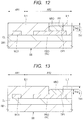
- FIG. 17 is a main-portion cross-sectional view of the semiconductor device during the manufacturing process thereof, which is subsequent to FIG. 16 ;
- FIG. 18 is a main-portion cross-sectional view of the semiconductor device during the manufacturing process thereof, which is subsequent to FIG. 17 ;
- FIG. 19 is a main-portion cross-sectional view of a semiconductor device in a studied example.
- FIG. 20 is a main-portion cross-sectional view of the semiconductor device in the studied example during the manufacturing process thereof;
- FIG. 21 is a main-portion cross-sectional view of the semiconductor device during the manufacturing process thereof, which is subsequent to FIG. 20 ;
- FIG. 22 is a main-portion cross-sectional view of the semiconductor device during the manufacturing process thereof, which is subsequent to FIG. 21 ;
- FIG. 23 is a main-portion cross-sectional view of the semiconductor device during the manufacturing process thereof, which is subsequent to FIG. 22 ;
- FIG. 24 is a main-portion cross-sectional view of a semiconductor device in a first modification
- FIG. 25 is a main-portion cross-sectional view of the semiconductor device in the first modification during the manufacturing process thereof;
- FIG. 26 is a main-portion cross-sectional view of the semiconductor device during the manufacturing process thereof, which is subsequent to FIG. 25 ;
- FIG. 27 is a main-portion cross-sectional view of the semiconductor device during the manufacturing process thereof, which is subsequent to FIG. 26 ;
- FIG. 28 is a main-portion cross-sectional view of the semiconductor device during the manufacturing process thereof, which is subsequent to FIG. 27 ;
- FIG. 29 is a main-portion cross-sectional view of the semiconductor device during the manufacturing process thereof, which is subsequent to FIG. 28 ;
- FIG. 30 is a main-portion cross-sectional view of the semiconductor device during the manufacturing process thereof, which is subsequent to FIG. 29 ;
- FIG. 31 is a main-portion cross-sectional view of the semiconductor device during the manufacturing process thereof, which is subsequent to FIG. 30 ;
- FIG. 32 is a main-portion cross-sectional view of the semiconductor device during the manufacturing process thereof, which is subsequent to FIG. 31 ;
- FIG. 33 is a main-portion cross-sectional view of a semiconductor device in a second modification
- FIG. 34 is a main-portion cross-sectional view of the semiconductor device in the second modification during the manufacturing process thereof;
- FIG. 35 is a main-portion cross-sectional view of the semiconductor device during the manufacturing process thereof, which is subsequent to FIG. 34 ;
- FIG. 36 is a main-portion cross-sectional view of the semiconductor device during the manufacturing process thereof, which is subsequent to FIG. 35 ;
- FIG. 37 is a main-portion cross-sectional view of the semiconductor device during the manufacturing process thereof, which is subsequent to FIG. 36 ;
- FIG. 38 is a main-portion cross-sectional view of the semiconductor device during the manufacturing process thereof, which is subsequent to FIG. 37 ;
- FIG. 39 is a main-portion cross-sectional view of the semiconductor device during the manufacturing process thereof, which is subsequent to FIG. 38 ;
- FIG. 40 is a main-portion cross-sectional view of the semiconductor device during the manufacturing process thereof, which is subsequent to FIG. 39 ;
- FIG. 41 is a main-portion cross-sectional view of a semiconductor device in a second embodiment
- FIG. 42 is a main-portion cross-sectional view of the semiconductor device in the second embodiment during the manufacturing process thereof;
- FIG. 43 is a main-portion cross-sectional view of the semiconductor device during the manufacturing process thereof, which is subsequent to FIG. 42 ;
- FIG. 44 is a main-portion cross-sectional view of the semiconductor device during the manufacturing process thereof, which is subsequent to FIG. 43 ;
- FIG. 45 is a main-portion cross-sectional view of the semiconductor device during the manufacturing process thereof, which is subsequent to FIG. 44 ;
- FIG. 47 is a main-portion cross-sectional view of the semiconductor device during the manufacturing process thereof, which is subsequent to FIG. 46 ;
- FIG. 48 is a main-portion cross-sectional view of the semiconductor device during the manufacturing process thereof, which is subsequent to FIG. 47 ;
- FIG. 49 is a main-portion cross-sectional view of the semiconductor device during the manufacturing process thereof, which is subsequent to FIG. 48 ;
- FIG. 50 is a main-portion cross-sectional view of the semiconductor device during the manufacturing process thereof, which is subsequent to FIG. 49 ;
- FIG. 51 is a main-portion cross-sectional view of the semiconductor device during the manufacturing process thereof, which is subsequent to FIG. 50 ;
- FIG. 52 is a main-portion cross-sectional view of a semiconductor device in a third embodiment
- FIG. 53 is a main-portion cross-sectional view of the semiconductor device in the third embodiment during the manufacturing process thereof;
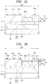
- FIG. 54 is a main-portion cross-sectional view of the semiconductor device during the manufacturing process thereof, which is subsequent to FIG. 53 ;
- FIG. 55 is a main-portion cross-sectional view of the semiconductor device during the manufacturing process thereof, which is subsequent to FIG. 54 ;
- FIG. 56 is a main-portion cross-sectional view of the semiconductor device during the manufacturing process thereof, which is subsequent to FIG. 55 ;
- FIG. 57 is a main-portion cross-sectional view of a semiconductor device in a third modification during the manufacturing process thereof.
- FIG. 58 is a main-portion cross-sectional view of the semiconductor device during the manufacturing process thereof, which is subsequent to FIG. 57 .
- each of the embodiments will be described by being divided into a plurality of sections or embodiments. However, they are by no means irrelevant to each other unless particularly explicitly described otherwise, but are in relations such that one of the sections or embodiments is modifications, details, supplementary explanation, and so forth of part or the whole of the others.
- FIG. 1 is a main-portion cross-sectional view showing a semiconductor device in an embodiment.
- FIGS. 2 and 3 are main-portion plan views of the semiconductor device in the present first embodiment.
- FIG. 2 shows a plan view of an area AR 1 .
- FIG. 3 shows a plan view of an area AR 2 .
- a cross-sectional view at a position along the line A 1 -A 1 in FIG. 2 corresponds to a cross section of the area AR 1 in FIG. 1 .
- a cross-sectional view at a position along the line A 2 -A 2 in FIG. 3 corresponds to a cross section of the area AR 2 in FIG. 1 .
- an optical waveguide WO 2 and semiconductor portions PRO and NRO are shown by the solid lines
- plugs PG 1 and PG 2 are shown by the broken lines
- wires M 1 a and M 1 b are shown by two-dot-dash lines.
- the semiconductor device in the present first embodiment has a base (supporting substrate) SB 1 , an insulating layer CL formed over the base SB 1 , and a semiconductor layer (second semiconductor layer) SL formed over the insulating layer CL.
- the base SB 1 , the insulating layer CL, and the semiconductor layer SL form an SOI (Silicon on Insulator) substrate SB.
- the base SB 1 is the supporting substrate supporting the insulating layer CL and a structure above the insulating layer CL, which is also a semiconductor substrate.
- the base SB 1 is preferably made of a monocrystalline silicon substrate, which is, e.g., a p-type monocrystalline silicon substrate having a (100) plane orientation and a specific resistance of about 5 to 50 ⁇ cm.
- the insulating layer CL is preferably made of a silicon oxide film.
- the insulating layer CL can also be regarded as a BOX (Buried Oxide) layer.
- the semiconductor layer SL is preferably made of a silicon layer (more specifically, a monocrystalline silicon layer) and can also be regarded as an SOI (Silicon on Insulator) layer.
- the SOI substrate SB has the area AR 1 and the area AR 2 .
- the area AR 1 and the area AR 2 correspond to the different two-dimensional areas of the main surface of the same SOI substrate SB.
- an optical signal transmission line (optical waveguide WO 1 ) is formed while, in the area AR 2 , an optical receiver (germanium optical receiver PD) is formed, the details of which will be described later.
- the area AR 1 and the area AR 2 may be or may not be adjacent to each other. However, for easier understanding, FIG. 1 shows the areas AR 1 and AR 2 which are adjacent in this order.
- the optical waveguide WO 1 as a transmission line for various optical signals is formed.
- the optical waveguide WO 1 is made of the semiconductor layer (silicon layer) SL and formed over the insulating layer CL.
- the lower surface of the optical waveguide WO 1 is in contact with the upper surface of the insulating layer CL.
- no impurity ion is implanted.
- the optical waveguide WO 1 is made of an intrinsic semiconductor, i.e., an i (intrinsic) type semiconductor.
- the optical waveguide WO 1 has a linear pattern extending in an X-direction.
- the optical signal introduced into the optical waveguide WO 1 travels in the optical waveguide WO 1 along the extending direction of the optical waveguide WO 1 , which applies also to the optical waveguide WO 2 described later.
- FIGS. 2 and 3 are orthogonal to each other and are also generally parallel with the main surface of the SOI substrate SB (or with the main surface of the base SB 1 ).
- a direction perpendicular to the paper surface with FIG. 1 corresponds to the X-direction.
- an interlayer insulating film IL 3 is formed so as to cover the optical waveguide WO 1 .
- the interlayer insulating film IL 3 is made of a silicon oxide film.
- the interlayer insulating film IL 3 is made of a multi-layer film including an insulating film IL 1 and an insulating film IL 2 over the insulating film IL 1 .
- each of the insulating film IL 1 and the insulating film IL 2 is made of a silicon oxide film.
- FIG. 1 shows the optical waveguide WO 1 having a quadrilateral (rectangular) cross-sectional shape.
- an interlayer insulating film IL 4 is formed.
- the germanium optical receiver (photoelectric conversion portion) PD formed in the area AR 2 .
- the germanium optical receiver PD is formed in the area AR 2 .
- the germanium optical receiver PD is a photoelectric conversion element (photoelectric conversion portion or photodetector) which converts an optical signal to an electric signal.
- the germanium optical receiver PD includes the p-type semiconductor portion (semiconductor layer) PRO and the n-type semiconductor portion (semiconductor layer) NRO.
- the p-type semiconductor portion PRO and the n-type semiconductor portion NRO form an element with a pn junction structure (diode with a pn structure) and thus form the germanium optical receiver PD.
- germanium a compound including germanium such as silicon germanium may also be used.
- the p-type semiconductor portion PRO is made of the semiconductor layer (silicon layer) SL and formed over the insulating layer CL.
- the lower surface of the p-type semiconductor portion PRO is in contact with the upper surface of the insulating layer CL.
- a p-type impurity is introduced in the p-type semiconductor portion PRO.
- the thickness (height) of the p-type semiconductor portion PRO is about the same as the thickness (height) of each of the waveguides WO 1 and WO 2 .
- the p-type semiconductor portion PRO is integrally coupled (connected) to the optical waveguide WO 2 .
- the p-type semiconductor portion PRO is integrally coupled (connected). This allows the optical signal that has propagated in the optical waveguide WO 2 to be introduced into the p-type semiconductor portion PRO.
- the optical waveguide WO 2 is made of the semiconductor layer SL and formed over the insulating layer CL. The lower surface of the optical waveguide WO 2 is in contact with the upper surface of the insulating layer CL. Note that the optical waveguide WO 2 is shown in FIG. 3 , but is not shown in the cross section of FIG. 1 .
- the optical waveguide WO 2 In the optical waveguide WO 2 , no impurity ion is implanted so that the optical waveguide WO 2 is made of an intrinsic semiconductor (i type semiconductor). In short, the optical waveguide WO 2 and the p-type semiconductor portion PRO are integrally formed and are each formed over the insulating layer CL. However, no impurity is introduced in the optical waveguide WO 2 , while a p-type impurity is introduced in the p-type semiconductor portion PRO.
- the germanium layer is made of n-type germanium, but it is also possible to introduce an impurity only into a portion of the surface of the germanium layer.
- a non-doped germanium layer is present under a doped germanium layer so that a pin junction type is formed.
- the germanium optical receiver PD has the p-type semiconductor portion PRO as a first semiconductor portion and a second semiconductor portion over the first semiconductor portion (p-type semiconductor portion PRO).
- the second semiconductor portion is made of the n-type semiconductor portion NRO.
- the second semiconductor portion included in the germanium optical receiver PD includes the germanium layer (semiconductor portion NRO) formed over the first semiconductor portion (p-type semiconductor portion PRO).
- the second semiconductor portion is formed in an opening OP 1 of the insulating film IL 1 .
- a thickness TH 2 of the second semiconductor portion (n-type semiconductor portion NRO) is smaller than a thickness TH 1 of the insulating film IL 1 over the first semiconductor portion (p-type semiconductor portion PRO).
- a contact hole CT 2 described later reaches the second semiconductor portion, and the plug PG 2 described later is electrically coupled to the second semiconductor portion.
- the interlayer insulating film IL 3 is formed so as to cover the germanium optical receiver PD (the p-type semiconductor portion PRO and the n-type semiconductor portion NRO).
- the insulating layer CL and the interlayer insulating film IL 3 can function as the clad layer.
- the insulating film IL 1 is not formed, but the insulating film IL 2 is formed. This is because, after the n-type semiconductor portion NRO is formed in the opening OP 1 formed in the insulating film IL 1 , the insulating film IL 2 is formed.
- the interlayer insulating film IL 3 located over the n-type semiconductor portion NRO is made of the insulating film IL 2
- the interlayer insulating film IL 3 other than that located over the n-type semiconductor portion NRO is made of a multi-layer film including the insulating film IL 1 and the insulating film IL 2 .
- the contact hole CT 1 is formed in the interlayer insulating film IL 3 (insulating films IL 1 and IL 2 ), while the contact hole CT 2 is formed in the insulating film IL 2 .
- the contact hole CT 1 formed in the interlayer insulating film IL 3 reaches the portion of the p-type semiconductor portion PRO which is uncovered with the n-type semiconductor portion NRO.
- the contact hole CT 2 formed in the insulating film IL 2 reaches the n-type semiconductor portion NRO.
- a portion of the upper surface of the n-type semiconductor portion NRO is exposed.
- the plug PG embedded in the contact hole CT 1 is referred to as the plug PG 1
- the plug PG embedded in the contact hole CT 2 is referred to as the plug PG 2
- wires M 1 are formed over the insulating film IL 2 in which the plugs PG 1 and PG 2 are embedded.
- the wires M 1 are first-layer wires and include the wires M 1 a and M 1 b.
- the lower surface of the plug PG 1 is in contact with the p-type semiconductor portion PRO and electrically coupled to the p-type semiconductor portion PRO.
- the upper surface of the plug PG 1 is in contact with the wire Mla and electrically coupled to the wire M 1 a .
- the lower surface of the plug PG 2 is in contact with the n-type semiconductor portion NRO and electrically coupled to the n-type semiconductor portion NRO.
- the upper surface of the plug PG 2 is in contact with the wire M 1 b and electrically coupled to the wire M 1 b . Consequently, the p-type semiconductor portion PRO is electrically coupled to the wire M 1 a via the plug PG 1 , while the n-type semiconductor portion NRO is electrically coupled to the wire M 1 b via the plug PG 2 .
- a DC current allowed to flow by a photovoltaic effect in the pn junction portion included in the germanium optical receiver PD can be extracted to the outside via the plugs PG 1 and PG 2 and the wires M 1 a and M 1 b .
- an optical signal can be extracted as an electric signal.
- the interlayer insulating film IL 4 is formed so as to cover the wires M 1 .
- a through hole (through opening) is formed and, in the through hole, a conductive plug PG 3 is embedded.
- a wire M 2 is formed over the interlayer insulating film IL 4 in which the plug PG 3 is embedded.
- the wire M 2 is a second-layer wire.
- the plug PG 3 is disposed between the wires M 1 and M 2 to electrically couple the wire M 1 and the wire M 2 to each other.
- a protective film TC is formed so as to cover the wire M 2 .
- the interlayer insulating film IL 4 is made of, e.g., a silicon oxide film. Silicon oxide is appropriate as the material of the clad layer.
- the protective film TC is made of, e.g., silicon oxynitride. The refractive index n of silicon oxide is about 1.45, while the refractive index n of silicon oxynitride is about 1.82.
- an opening OP 2 exposing a portion of the wire M 2 is formed. The portion of the wire M 2 which is exposed from the opening OP 2 serves as a pad portion (bonding pad or external coupling portion).
- FIGS. 4 to 18 are main-portion cross-sectional views of the semiconductor device in the present first embodiment during the manufacturing process thereof, which show cross sections equivalent to that shown in FIG. 1 described above.
- the SOI substrate SB including the base (supporting substrate) SB 1 , the insulating layer CL formed over the base SB 1 , and the semiconductor layer SL formed over the insulating layer CL is provided.
- the base SB 1 is preferably made of a monocrystalline silicon substrate.
- the insulating layer CL is preferably made of a silicon oxide film and has a thickness of, e.g., about 2 to 3 ⁇ m.
- the semiconductor layer SL is preferably made of a silicon layer (more specifically, a monocrystalline silicon layer) and has a thickness of, e.g., about 180 to 250 nm.
- a method of manufacturing the SOI substrate SB is not limited, and the SOI substrate SB can be manufactured using, e.g., an SIMOX (Silicon Implanted Oxide) method, a bonding method, a smart cut process, or the like.
- the optical waveguide WO 1 and the semiconductor portion PRO can be formed. Subsequently, the photoresist pattern is removed by asking or the like.
- Each of the optical waveguide WO 1 and the semiconductor portion PRO is made of the patterned semiconductor layer SL and formed over the insulating layer CL.
- the optical waveguides WO 1 and WO 2 and the semiconductor portion PRO have not been doped with any impurity. Note that the optical waveguide WO 2 is not shown in the cross sections of FIGS. 4 to 18 , but is shown in FIG. 3 described above.
- the optical waveguide WO 2 is formed integrally with the semiconductor portion PRO.
- the semiconductor portion PRO is changed into the p-type semiconductor portion PRO.
- a photoresist pattern formed using a photolithographic technique as a mask ion implantation inhibiting mask
- a p-type impurity is ion-implanted into the semiconductor portion PRO.
- the p-type semiconductor portion PRO is formed. Note that, during the ion implantation, the optical waveguides WO 1 and WO 2 are covered with the photoresist pattern, and therefore the p-type impurity (or an n-type impurity) is not implanted therein.
- heat treatment for activating the introduced impurities can also be performed.
- the insulating film IL 1 is formed so as to cover the optical waveguides WO 1 and WO 2 and the semiconductor portion PRO.
- the insulating film IL 1 is preferably made of a silicon oxide film, and is more preferably made of a high-quality (high-density) silicon oxide film. By forming the insulating film IL 1 of the high-quality (high-density) silicon oxide film, it is possible to allow the insulating film IL 1 to function as the clad layer, as described above.
- the insulating film IL 1 is formed using, e.g., an LPCVD (Low-Pressure Chemical Vapor Deposition) method.
- the LPCVD method allows a high-quality (high-density) silicon oxide film to be formed.
- As a raw material gas for the LPCVD method e.g., monosilane and dinitrogen monoxide, only TEOS (Tetraethyl orthosilicate), TEOS and oxygen, or the like is used.
- a deposition temperature for the insulating film IL 1 is, e.g., 600 to 700° C.
- the thickness of the formed insulating film IL 1 is larger than the thickness of the semiconductor layer SL and is about 1 ⁇ m.
- the silicon oxide film formed by the LPCVD method has a low throughput
- a multi-layer film including the silicon oxide film formed by the LPCVD method and a silicon oxide film formed by a PECVD (Plasma-Enhanced Chemical Vapor Deposition) method and having a high throughput may also be used.
- the upper surface of the insulating film IL 1 is subjected to polishing using a CMP (Chemical Mechanical Polishing) method or the like to be planarized. Even when the upper surface of the insulating film IL 1 is polished, the optical waveguides WO 1 and WO 2 and the semiconductor portion PRO are not exposed. Note that the thickness TH 1 of the insulating film IL 1 over the p-type semiconductor portion PRO is a thickness after the insulating film IL 1 is planarized. The thickness TH 1 of the insulating film IL 1 is about 700 nm.
- the opening OP 1 is formed in the insulating film IL 1 .
- the two-dimensional size (area) of the opening OP 1 is smaller than the two-dimensional size of the p-type semiconductor portion PRO.
- the opening OP 1 is included in the p-type semiconductor portion PRO in plan view.
- the opening OP 1 extends through the insulating film IL 1 to reach the semiconductor portion PRO. At the bottom portion of the opening OP 1 , a portion of the upper surface of the semiconductor portion PRO is exposed.
- the n-type semiconductor portion NRO can be formed using an epitaxial growth method.
- the n-type semiconductor portion NRO is selectively formed over the p-type semiconductor portion PRO.
- Such a formation method is particularly referred to as a selective epitaxial growth method (the details of which will be described later).
- the n-type semiconductor portion NRO can be formed by epitaxially growing a germanium layer containing an n-type impurity.
- the n-type semiconductor portion NRO can also be formed by epitaxially growing a germanium layer made of an intrinsic semiconductor and then introducing an n-type impurity into the germanium layer by an ion implantation method or the like.
- an element having a pn junction structure including the p-type semiconductor portion PRO made of silicon and the n-type semiconductor portion NRO made of germanium is formed.
- the n-type semiconductor portion (germanium layer) NRO formed by the epitaxial growth method has a generally trapezoidal cross-sectional shape.
- the thickness TH 2 of the n-type semiconductor portion NRO is smaller than the thickness TH 1 of the insulating film IL 1 over the p-type semiconductor portion PRO.
- the upper surface of the n-type semiconductor potion NRO is lower in level than the upper surface of the insulating film IL 1 .
- the insulating film IL 1 is formed over the p-type semiconductor portion PRO such that the thickness TH 1 thereof is larger than the thickness TH 2 of the n-type semiconductor portion NRO.
- the thickness TH 2 of the n-type semiconductor portion NRO is about 500 nm.
- the selectivity of the selective epitaxial growth method collapses so that, over the insulating film IL 1 , semiconductor particles SP 1 made of the same material as that of the n-type semiconductor portion NRO, i.e., germanium are formed.
- a photoresist film (second insulating film) PR is formed over the insulating film IL 1 including the n-type semiconductor portion NRO.
- the photoresist film PR is embedded in the opening OP 1 to overlie the n-type semiconductor portion NRO.
- the photoresist film PR is removed from over the insulating film IL 1 to be left only over the n-type semiconductor portion NRO in the opening OP 1 .
- a method of removing the photoresist film PR a method which does not damage the insulating film IL 1 is preferably used.
- a resist etch-back process using an O 2 plasma or the like is used preferably.
- the photoresist film PR over the insulating film IL 1 may also be removed by a resist CMP method. In this case also, the photoresist film PR can be left only over the n-type semiconductor portion NRO in the opening OP 1 .
- the semiconductor particles SP 1 are removed from over the insulating film IL 1 .
- the n-type semiconductor portion NRO made of the same material as that of the semiconductor particles SP 1 is covered herein with the photoresist film PR and the insulating film IL 1 , and are therefore not removed.
- Examples of a method of removing the semiconductor particles SP 1 include dry etching and wet etching.
- dry etching using a halogen-based gas is used as a method which does not damage the insulating film IL 1 and the photoresist film PR.
- the photoresist film PR in the opening OP 1 is removed by asking or the like.
- the insulating film IL 2 is formed over the insulating film IL 1 including the n-type semiconductor portion NRO.
- the upper surface of the insulating film IL 2 is subjected to polishing using a CMP method or the like to be planarized.
- the insulating film IL 2 is preferably made of a silicon oxide film, and is more preferably made of a silicon oxide film with excellent embeddability.
- the insulating film IL 2 is preferably formed using an SACVD (Sub Atmosphere Chemical Vapor Deposition) method using O 3 -TEOS as a raw material gas or an SOG (Spin On Glass) method.
- an inorganic material such as polysilazane mentioned above or HSQ (Hydrogen Silsesquioxane) or an organic material such as MSQ (Methyl Silsesquioxane) is used preferably.
- the interlayer insulating film IL 3 is made of a multi-layer film including the insulating film IL 1 and the insulating film IL 2 over the insulating film IL 1 .
- the insulating film IL 2 is formed, but the insulating film IL 1 is not formed. Consequently, the interlayer insulating film IL 3 located over the n-type semiconductor portion NRO is made of the insulating film IL 2 , while the interlayer insulating film IL 3 other than that located over the n-type semiconductor portion NRO is made of the multi-layer film including the insulating film IL 1 and the insulating film IL 2 .
- the interlayer insulating film IL 3 is formed over the insulating layer CL so as to cover the optical waveguide WO 1 , the optical waveguide WO 2 , the p-type semiconductor portion PRO, and the n-type semiconductor portion NRO.
- the contact hole CT 1 is included in the portion of the p-type semiconductor portion PRO which is uncovered with the n-type semiconductor portion NRO in plan view.
- the contact hole CT 1 extends through the interlayer insulating film IL 3 (insulating films IL 2 and IL 1 ) to reach the p-type semiconductor portion PRO.
- the contact hole CT 2 is included in the n-type semiconductor portion NRO in plan view.
- the contact hole CT 2 extends through the interlayer insulating film IL 3 (insulating film IL 2 ) to reach the n-type semiconductor portion NRO.
- a portion of the upper surface of the n-type semiconductor portion NRO is exposed.
- the contact holes CT can be formed as follows. First, over the interlayer insulating film IL 3 , a photoresist pattern (not shown) is formed using a photolithographic technique. The photoresist pattern has respective openings for the contact holes CT 1 and CT 2 . Then, by etching the interlayer insulating film IL 3 using the photoresist pattern as an etching mask, the contact holes CT 1 and CT 2 can be formed in the interlayer insulating film IL 3 . Then, the photoresist pattern is removed by asking or the like. In this case, the contact holes CT 1 and CT 2 are formed together in the same step.
- the conductive plugs PG (PG 1 and PG 2 ) are formed (embedded).
- the plugs PG can be formed as follows. First, over the interlayer insulating film IL 3 (insulating film IL 2 ) including the bottom surfaces and side walls of the contact holes CT, a conductor film made of a tungsten film or the like is formed so as to be embedded in the contact holes CT. Then, the unneeded conductor film outside the contact holes CT is removed by a CMP method, an etch-back method, or the like to allow the plugs PG to be formed.
- the conductor film may also be a multi-layer film including a barrier conductor film such as a titanium film or a titanium nitride film and a tungsten film.
- the barrier conductor film is formed over the interlayer insulating film IL 3 (insulating film IL 2 ) including the bottom surfaces and side walls of the contact holes CT, and then a main conductor film made of a tungsten film is formed over the barrier conductor film so as to be embedded in the contact holes CT.
- the plug PG embedded in the contact hole CT 1 is the plug PG 1 .
- the plug PG 1 is disposed over the p-type semiconductor portion PRO and is in contact with and electrically coupled to the p-type semiconductor portion PRO.
- the plug PG embedded in the contact hole CT 2 is the plug PG 2 .
- the plug PG 2 is disposed over the n-type semiconductor portion NRO and is in contact with and electrically coupled to the n-type semiconductor portion NRO.
- the wires M 1 are formed.
- the wires M 1 can be formed as follows. First, over the interlayer insulating film IL 3 in which the plugs PG are embedded, a conductive film for forming the wires M 1 is formed.
- the conductive film is made of, e.g., a multi-layer film including a barrier conductor film, a main conductor film thereover, and a barrier conductor film thereover.
- the barrier conductor film is made of a titanium film, a titanium nitride film, or a multi-layer film thereof.
- the main conductor film is made of an aluminum film or an aluminum alloy film. Then, over the conductive film, a photoresist pattern is formed using a photolithographic technique.
- the wires M 1 can be formed. Subsequently, the photoresist pattern is removed by asking or the like.
- the wires M 1 are made of the patterned conductive film. When the wires M 1 are formed, the respective upper surfaces of the plugs PG come into contact with the wires M 1 so that the plugs PG are electrically coupled to the wires M 1 thereover.
- the wires M 1 include the foregoing wires M 1 a and M 1 b .
- the wire M 1 a is electrically coupled to the p-type semiconductor portion PRO via the plug PG 1 .
- the wire M 1 b is electrically coupled to the n-type semiconductor portion NRO via the plug PG 2 .
- the interlayer insulating film IL 4 is formed so as to cover the wires M 1 .
- the upper surface of the interlayer insulating film IL 4 is subjected to polishing using a CMP method or the like to be planarized.
- the interlayer insulating film IL 4 is preferably made of a silicon oxide film and can be formed using, e.g., a CVD method.
- a through hole (through opening) is formed in the interlayer insulating film IL 4 .
- the conductive plug PG 3 is formed (embedded).
- the plug PG 3 can be formed by substantially the same method as used to form the foregoing plugs PG.
- the wire M 2 is formed over the interlayer insulating film IL 4 in which the plug PG 3 is embedded.
- the wire M 2 can be formed by substantially the same method as used to form the wires M 1 .
- a conductive film for forming the wire M 2 is formed over the interlayer insulating film IL 4 in which the plug PG 3 is embedded.
- the wire M 2 can be formed.
- the plug PG 3 is disposed between the wire M 2 and the wire M 1 to electrically couple the wire M 2 to the wire M 1 .
- the protective film TC is formed so as to cover the wire M 2 .
- the protective film TC is made of, e.g., a silicon oxynitride film and can be formed using a CVD method or the like.
- the opening OP 2 is formed in the protective film TC. From the opening OP 2 of the protective film TC, a portion of the wire M 2 is exposed. The portion of the wire M 2 exposed from the opening OP 2 serves as the pad portion (bonding pad or external coupling portion). Then, the SOI substrate SB is diced (cut) together with the structure located thereabove to be singulated, whereby semiconductor chips (semiconductor devices) are acquired.
- the semiconductor device in the present first embodiment can be manufactured.
- FIG. 19 is a main-portion cross-sectional view of the semiconductor device in the studied example studied by the present inventors.
- the structure of the area AR 1 which is included in the region equivalent to that in FIG. 1 described above is the same as in the semiconductor device in the present first embodiment. Accordingly, FIG. 19 shows only the cross-sectional view of the area AR 2 which is included in the region equivalent to that in FIG. 1 described above. Note that, in FIG. 19 , for simpler illustration, the depiction of the foregoing contact holes CT, the plugs PG, the interlayer insulating film IL 4 , and the structure located thereabove is omitted.
- the semiconductor device in the studied example shown in FIG. 19 includes the base SB 1 , the insulating layer CL formed over the base SB 1 , the optical waveguides WO 1 and WO 2 and the semiconductor portion PRO which are formed over the insulating layer CL, and the semiconductor portion NRO formed over the semiconductor portion PRO, similarly to the semiconductor device in the present first embodiment.
- the optical waveguide WO 2 is shown in FIG. 3 described above, but is not shown in FIGS. 1 and 19 described above.
- an interlayer insulating film IL 103 (insulating films IL 101 and IL 102 ) is formed, and the semiconductor device in the studied example is different from that in the present first embodiment in the insulating films IL 101 and IL 102 .
- the thickness TH 2 of the n-type semiconductor portion NRO is smaller than the thickness TH 1 of the insulating film IL 1 over the p-type semiconductor portion PRO.
- a thickness TH 102 of the n-type semiconductor portion NRO is larger than a thickness TH 101 of the insulating film IL 101 over the p-type semiconductor portion PRO.
- FIGS. 20 to 23 are main-portion cross-sectional views of the semiconductor device in the studied example during the manufacturing process thereof, which show cross sections equivalent to that shown in FIG. 19 described above. That is, FIGS. 20 to 23 show only the cross-sectional views of the area AR 2 , similarly to FIG. 19 .
- the manufacturing process of the semiconductor device in the studied example is also substantially the same as the manufacturing process of the semiconductor device in the present first embodiment described above until the structure in FIG. 20 equivalent to FIG. 5 described above is obtained by patterning the semiconductor layer SL to form the semiconductor portion PRO and then introducing a p-type impurity into the semiconductor portion PRO using an ion implantation method or the like to change the semiconductor portion PRO into the p-type semiconductor portion PRO.
- the insulating film IL 101 is formed so as to cover the optical waveguides WO 1 and WO 2 and the semiconductor portion PRO, as shown in FIG. 21 .
- the thickness of the insulating film IL 101 is about 200 nm.
- an opening OP 101 is formed in the insulating film IL 101 .
- the two-dimensional size (area) of the opening OP 101 is smaller than the two-dimensional size of the p-type semiconductor portion PRO.
- the opening OP 101 is included in the p-type semiconductor portion PRO in plan view.
- the opening OP 101 extends through the insulating film IL 101 to reach the semiconductor portion PRO. At the bottom portion of the opening OP 101 , a portion of the upper surface of the semiconductor portion PRO is exposed.
- the n-type semiconductor portion (germanium layer) NRO made of germanium (Ge) is formed over the p-type semiconductor portion PRO exposed at the bottom portion of the opening OP 101 .
- the n-type semiconductor portion NRO can be formed using an epitaxial growth method.
- the n-type semiconductor portion NRO is formed selectively over the p-type semiconductor portion PRO.
- an element having a pn junction structure including the p-type semiconductor portion PRO made of a silicon layer and the n-type semiconductor portion NRO made of the germanium layer is formed.
- the n-type semiconductor portion (germanium layer) NRO formed by the epitaxial growth method has a generally trapezoidal cross-sectional shape.
- the thickness TH 2 of the n-type semiconductor portion NRO formed herein is about 500 nm and larger than the thickness TH 101 of the insulating film IL 101 over the p-type semiconductor portion PRO.
- the selectivity of the selective epitaxial growth method collapses so that the semiconductor particles SPI made of germanium are formed over the insulating film IL 101 .
- the insulating film IL 102 is formed over the insulating film IL 101 including the n-type semiconductor portion NRO. Then, the upper surface of the insulating film IL 102 is planarized by a CMP method or the like. A combination of the insulating film IL 101 and the insulating film IL 102 corresponds to the interlayer insulating film IL 103 . Then, in the interlayer insulating film IL 103 , contact holes are formed and, in the contact holes, conductive plugs are formed. The plugs couple the p-type semiconductor portion PRO and the n-type semiconductor portion NRO to wires in layers located thereabove. The depiction and description of the contact holes, the plugs, and the wires is omitted herein.
- the present inventors have considered introducing the germanium optical receiver PD into a semiconductor device to which a silicon photonics technique is applied. This entails the need to form the n-type semiconductor portion NRO made of germanium over the p-type semiconductor portion PRO made of silicon.
- a selective epitaxial growth method is used preferably. As described above, the selective epitaxial growth method allows for selective epitaxial growth of only a portion of a surface.
- a mixture gas obtained by mixing an appropriate amount of hydrogen chloride as an etching gas in a raw material gas made of germanium hydride is allowed to flow.
- hydrogen chloride inhibits nuclear growth of germanium so that single crystal growth of a germanium layer selectively proceeds only over the semiconductor layer.
- the germanium layer forming the n-type semiconductor portion NRO can be formed over the p-type semiconductor layer PRO made of silicon.
- the semiconductor particles SP 1 made of the same material (which is germanium herein) as that of the n-type semiconductor portion NRO are undesirably formed over the insulating film IL 101 .
- the insulating film IL 102 is formed, resulting in a state where the semiconductor particles SP 1 remain between the insulating film IL 101 and the insulating film IL 102 .
- the presence of the semiconductor particles SP 1 between the insulating film IL 101 and the insulating film IL 102 may cause a problem.
- the probability is increased that diffused reflection by the semiconductor particles SP 1 and the degraded adhesion between the insulating film IL 101 and the insulating film IL 102 cause a loss in the optical property of the germanium optical receiver PD (e.g., light leaks from the p-type semiconductor portion PRO and the n-type semiconductor portion NRO to the surroundings), resulting in the degraded reliability of the semiconductor device.
- it is desired to improve the reliability of the semiconductor device by controlling formation conditions in the epitaxial growth and thus preventing the semiconductor particles SP 1 from being formed or by removing the formed semiconductor particles SP 1 .
- the n-type semiconductor portion NRO made of the same material (germanium) as that of the semiconductor particles SP 1 is exposed, as shown in FIG. 19 . Accordingly, when the semiconductor particles SP 1 are to be removed by the etching, the n-type semiconductor portion NRO is also etched.
- the thickness TH 102 of the n-type semiconductor portion NRO is larger than the thickness TH 101 of the insulating film IL 101 over the p-type semiconductor portion PRO. If the n-type semiconductor portion NRO is to be masked with a resist film or the like, the semiconductor particles SP 1 over the insulating film IL 101 are also covered with a resist film or the like and, in that state, the semiconductor particles SP 1 cannot be removed.
- the main characteristic feature of the present first embodiment is that, as shown in FIGS. 1 and 9 , the thickness TH 2 of the n-type semiconductor portion (first semiconductor layer) NRO formed in the opening OP 1 of the insulating film (first insulating film) IL 1 is set smaller than the thickness TH 1 of the insulating film IL 1 over the p-type semiconductor portion PRO.
- the upper surface of the n-type semiconductor portion NRO is set lower in level than the upper surface of the insulating film IL 1 .
- the thickness TH 1 of the insulating film IL 1 over the p-type semiconductor portion PRO is set larger than the thickness TH 2 of the n-type semiconductor portion NRO.
- the photoresist film (second insulating film) PR is formed over the insulating film IL 1 and the n-type semiconductor portion NRO and, as shown in FIG. 11 , the photoresist film PR is removed from over the insulating film IL 1 , while being left over the n-type semiconductor portion NRO in the opening OP 1 of the insulating film IL 1 .
- the reliability of the semiconductor device can be improved.
- the following is a specific description of the reason for this.
- the photoresist film PR is embedded in the opening OP 1 of the insulating film IL 1 to overlie the n-type semiconductor portion NRO. Subsequently, the photoresist film PR is etched (etched back) in accordance with the upper surface of the insulating film IL 1 . By doing so, as shown in FIG. 9 , by setting the thickness TH 2 of the n-type semiconductor portion (first semiconductor layer) NRO formed in the opening OP 1 of the insulating film (first insulating film) IL 1 smaller than the thickness TH 1 of the insulating film IL 1 over the p-type semiconductor portion PRO, as shown in FIG. 10 , the photoresist film PR is embedded in the opening OP 1 of the insulating film IL 1 to overlie the n-type semiconductor portion NRO. Subsequently, the photoresist film PR is etched (etched back) in accordance with the upper surface of the insulating film IL 1 . By doing so, as shown in FIG.
- the upper surface of the insulating film IL 1 is subjected to polishing using a CMP method or the like to be planarized. If the upper surface of the insulating film IL 1 is not planarized, when the opening OP 1 is subsequently formed in the insulating film IL 1 and the n-type semiconductor portion NRO is formed in the opening OP 1 by an epitaxial growth method, the semiconductor particles SP 1 are formed concurrently in and over the depressed portion and the protruding portion of the upper surface of the insulating film IL 1 (see FIG. 6 ).
- the photoresist film PR is formed over the insulating film Il 1 and then etched (etched back) in accordance with the protruding portion of the upper surface of the insulating film IL 1 .
- the photoresist film PR remains in the depressed portion of the upper surface of the insulating film IL 1 .
- the semiconductor particles SP 1 formed in the depressed portion of the upper surface of the insulating film IL 1 cannot be removed by the subsequent etching.
- the photoresist film PR is to be etched (etched back) in accordance with the depressed portion of the upper surface of the insulating film IL 1 , the photoresist film PR in the opening OP 1 is also etched. Consequently, it becomes difficult to control the amount of etching of the photoresist film PR so as to leave the photoresist film PR only over the n-type semiconductor portion NRO in the opening OP 1 of the insulating film IL 1 .
- the upper surface of the insulating film IL 1 is planarized to allow the amount of etching of the photoresist film PR to be easily controlled.
- the photoresist film PR can be left only over the n-type semiconductor portion NRO in the opening OP 1 of the insulating film IL 1 .
- the photoresist film PR is formed over the insulating film IL 1 including the n-type semiconductor portion NRO, but the film formed over the insulating film IL 1 including the n-type semiconductor portion NRO is not limited to the photoresist film PR.
- a silicon oxide film may also be formed over the insulating film IL 1 including the n-type semiconductor portion NRO by an SOG method with excellent embeddability.
- FIG. 24 is a main-portion cross-sectional view of the semiconductor device in the first modification.
- the semiconductor device in the first modification is a higher-concept version of the semiconductor device in FIG. 1 described above.
- the semiconductor device in the first embodiment has been described as the semiconductor device to which a silicon photonics technique is applied by way of example.
- the semiconductor device in the first embodiment is applicable to a versatile semiconductor device.
- the semiconductor device in the first modification includes the base (supporting substrate) SB 1 , the insulating film IL 1 formed over the base SB 1 , and a semiconductor layer (first semiconductor layer) EP formed over the base SB 1 .
- the semiconductor layer EP is formed in the opening OP 1 of the insulating film IL 1 .
- a thickness TH 4 of the semiconductor layer EP is smaller than the thickness TH 1 of the insulating film IL 1 .
- the insulating film IL 2 is formed so as to cover the semiconductor layer EP. Note that, between the base SB 1 and the insulating film IL 1 , another layer may also be formed, though not shown.
- FIGS. 25 to 32 are main-portion cross-sectional views of the semiconductor device in the first modification during the manufacturing process thereof, which show cross sections equivalent to that shown in FIG. 24 described above.
- the semiconductor substrate SB including the base (supporting substrate) SB 1 is provided.
- the base SB 1 any substrate may be used as long as the semiconductor layer EP can be epitaxially grown over the main surface thereof.
- the base SB 1 is made of a conductor substrate or a semiconductor substrate.
- the substrate SB may also be a substrate having another layer formed over a base and having a conductor layer or a semiconductor layer (first layer) in the uppermost layer (upper surface) thereof. In this case, the semiconductor layer is epitaxially grown over the upper surface of the conductor layer or the semiconductor layer.
- the insulating film IL 1 is preferably made of a silicon oxide film and can be formed using, e.g., a CVD method.
- the opening OP 1 is formed in the insulating film IL 1 .
- the opening OP 1 extends through the insulating film IL 1 to reach the base SB 1 .
- a portion of the upper surface of the base SB 1 is exposed.
- the semiconductor layer EP is formed over the base SB 1 exposed at the bottom portion of the opening OP 1 .
- the semiconductor layer EP is made of, e.g., silicon, silicon germanium, or germanium.
- the semiconductor layer EP can be formed using an epitaxial growth method.
- the semiconductor layer EP is selectively formed over the base SB 1 .
- the thickness TH 4 of the semiconductor layer EP is smaller than the thickness TH 1 of the insulating film IL 1 .
- the upper surface of the semiconductor layer EP is lower in level than the upper surface of the insulating film IL 1 .
- the insulating film IL 1 is formed such that the thickness TH 1 thereof is larger than the thickness TH 4 of the semiconductor layer EP.
- the selectivity of the selective epitaxial growth method collapses so that, over the insulating film IL 1 , the semiconductor particles SP 1 made of the same material as that of the semiconductor layer EP are formed.
- the photoresist film (second insulating film) PR is formed over the insulating film IL 1 including the semiconductor layer EP.
- the photoresist film PR is embedded in the opening OP 1 to overlie the semiconductor layer EP.
- the photoresist film PR is removed from over the insulating film IL 1 to be left only over the semiconductor portion EP in the opening OP 1 .
- a method of removing the photoresist film PR a method which does not damage the insulating film IL 1 is used preferably.
- a resist etch-back process using an O 2 plasma or the like is used preferably.
- the photoresist film PR may also be removed from over the insulating film IL 1 by a resist CMP method. In this case also, the photoresist film PR can be left only over the semiconductor portion EP in the opening OP 1 .
- the semiconductor particles SP 1 are removed from over the insulating film IL 1 .
- the semiconductor layer EP made of the same material as that of the semiconductor particles SP 1 is covered with the photoresist film PR and the insulating film IL 1 , and is therefore not removed.
- the method of removing the semiconductor particles SP 1 include dry etching and wet etching.
- dry etching using a halogen-based gas is used as a method which does not damage the insulating film IL 1 and the photoresist film PR.
- the photoresist film PR in the opening OP 1 is removed by asking or the like.
- the insulating film IL 2 is formed over the insulating film IL 1 including the semiconductor layer EP.
- the insulating film IL 2 is formed.
- the upper surface of the insulating film IL 2 is subjected to polishing using a CMP method or the like to be planarized.
- the insulating film IL 2 is made of a silicon oxide film and can be formed using, e.g., a CVD method.
- the contact holes, the plugs, and the wires are formed, but the depiction and illustration thereof is omitted.
- the thickness TH 4 of the semiconductor layer EP formed in the opening OP 1 of the insulating film IL 1 is set smaller than the thickness TH 1 of the insulating film IL 1 .
- the photoresist film PR is embedded in the opening OP 1 of the insulating film IL 1 to overlie the semiconductor layer EP.
- the photoresist film PR is etched (etched back) in accordance with the upper surface of the insulating film IL 1 .
- the manufacturing method of the semiconductor device in the first modification is widely applicable to the case where the semiconductor layer is formed in the opening of the insulating film by the epitaxial growth method.
- FIG. 33 is a main-portion cross-sectional view of the semiconductor device in the second modification.
- the configuration of the semiconductor device in the second modification is the same as that of the semiconductor device in the foregoing first embodiment except for the germanium optical receiver formed in the area AR 2 shown in FIG. 1 . Accordingly, a repeated description is omitted, and a description will be given herein of the configuration of the area AR 2 .
- FIG. 33 shows only the cross-sectional view of the area AR 2 . Note that, in FIG. 33 , for simpler illustration, the depiction of the contact holes CT, the plugs PG, the interlayer insulating film IL 4 , and the structure located thereabove is omitted.
- the semiconductor device in the second modification shown in FIG. 33 includes the base SB 1 , the insulating layer CL formed over the base SB 1 , the optical waveguides WO 1 and WO 2 and the p-type semiconductor portion PRO which are formed over the insulating layer CL, and the n-type semiconductor portion NRO formed over the p-type semiconductor portion PRO, similarly to the semiconductor device in the foregoing first embodiment.
- the optical waveguide WO 2 is shown in FIG. 3 described above, but is not shown in FIGS. 1 and 33 described above.
- the semiconductor device in the second modification shown in FIG. 33 is different from the semiconductor device in the first embodiment in that, over the n-type semiconductor portion NRO, i.e., between the n-type semiconductor portion NRO and the insulating film IL 2 , a cap layer CP is formed.
- the cap layer CP is made of silicon (Si) or silicon germanium (SiGe). More preferably, the cap layer CP is made of silicon (Si).
- the two-dimensional shape of the cap layer CP substantially coincides with the two-dimensional shape of the n-type semiconductor portion NRO.
- a thickness TH 3 of the cap layer CP is, e.g., not more than 50 nm, and is preferably about 10 to 30 nm. It is also possible to regard a combination of the n-type semiconductor portion NRO and the cap layer CP thereover as a semiconductor portion.
- the germanium optical receiver PD in the second modification includes the p-type semiconductor portion PRO as the first semiconductor portion and the second semiconductor portion over the first semiconductor portion (p-type semiconductor portion PRO).
- the second semiconductor portion has a multi-layer structure including the n-type semiconductor portion NRO and the cap layer CP.
- the second semiconductor portion included in the germanium optical receiver PD includes the germanium layer (semiconductor portion NRO) formed over the first semiconductor portion (p-type semiconductor portion PRO), and further includes the silicon layer (cap layer CP) formed over the germanium layer (semiconductor portion NRO).
- the second semiconductor portion is formed in the opening OP 1 of the insulating film IL 1 .
- the total thickness of the thickness TH 2 of the n-type semiconductor portion NRO and the thickness TH 3 of the cap layer CP is smaller than the thickness TH 1 of the insulating film IL 1 over the p-type semiconductor portion PRO.
- the interlayer insulating film IL 3 is formed so as to cover the germanium optical receiver PD (the p-type semiconductor portion PRO, the n-type semiconductor portion NRO, and the cap layer CP).
- the insulating layer CL and the interlayer insulating film IL 3 are allowed to function as a clad layer.
- the insulating film IL 1 is not formed, but the insulating film IL 2 is formed. This is because, after the multi-layer structure including the n-type semiconductor portion NRO and the cap layer CP is formed in the opening OP 1 formed in the insulating film IL 1 , the insulating film IL 2 is formed. Consequently, the interlayer insulating film IL 3 located over the cap layer CP is made of the insulating film IL 2 , while the interlayer insulating film IL 3 other than that located over the cap layer CP is made of the multi-layer film including the insulating film IL 1 and the insulating film IL 2 .
- FIGS. 34 to 40 are main-portion cross-sectional views of the semiconductor device in the second modification during the manufacturing process thereof, which show cross sections equivalent to that shown in FIG. 33 described above. In other words, FIGS. 34 to 40 show only the cross-sectional views of the area AR 2 , similarly to FIG. 33 .
- the n-type semiconductor portion (germanium layer) NRO made of germanium (Ge) is formed over the p-type semiconductor portion PRO exposed at the bottom portion of the opening OP 1 .
- the n-type semiconductor portion NRO can be formed using an epitaxial growth method.
- the n-type semiconductor portion NRO is selectively formed over the p-type semiconductor portion PRO.
- an element having a pn junction structure including the p-type semiconductor portion PRO made of silicon and the n-type semiconductor portion NRO made of germanium is formed.
- the n-type semiconductor portion (germanium layer) NRO formed by the epitaxial growth method has a generally trapezoidal cross-sectional shape.
- the selectivity of the selective epitaxial growth method collapses so that the semiconductor particles SP 1 made of the same material as that of the n-type semiconductor portion NRO, i.e., germanium are formed over the insulating film IL 1 .
- the cap layer CP is selectively formed over the n-type semiconductor portion NRO.
- the cap layer CP can be formed by, e.g., epitaxially growing a semiconductor layer (semiconductor layer for the cap layer CP) made of silicon (Si) over the n-type semiconductor portion NRO, and then introducing an n-type impurity into the semiconductor layer using an ion implantation method.
- the cap layer CP is made of an n-type silicon layer.
- the total thickness of the thickness TH 2 of the n-type semiconductor portion NRO and the thickness TH 3 of the cap layer CP is smaller than the thickness TH 1 of the insulating film IL 1 over the p-type semiconductor portion PRO.
- the upper surface of the cap layer CP is lower in level than the upper surface of the insulating film IL 1 .
- the insulating film IL 1 is formed over the p-type semiconductor portion PRO such that the thickness TH 1 thereof is larger than the total thickness of the thickness TH 2 of the n-type semiconductor portion NRO and the thickness TH 3 of the cap layer CP.
- the selectivity of the selective epitaxial growth method collapses so that semiconductor particles SP 2 made of the same material (which is silicon herein) as that of the cap layer CP are formed over the insulating film IL 1 .
- the semiconductor particles SP 2 come in two types, i.e., the semiconductor particles SP 2 formed directly over the insulating film IL 1 and the semiconductor particles SP 2 formed over the semiconductor particles SP 1 using the semiconductor particles SP 1 over the insulating film IL 1 as nucleus.
- the photoresist film (second insulating film) PR is formed over the insulating film IL 1 including the cap layer CP.
- the photoresist film PR is embedded in the opening OP 1 to overlie the cap layer CP.
- the photoresist film PR is removed from over the insulating film IL 1 to be left only over the cap layer CP in the opening OP 1 .
- a method of removing the photoresist film PR a method which does not affect the insulating film IL 1 and the cap layer CP is used preferably.
- a resist etch-back process using an O 2 plasma or the like is used preferably.
- the semiconductor particles SP 1 and the semiconductor particles SP 2 are removed from over the insulating film IL 1 .
- the n-type semiconductor portion NRO made of the same material as that of the semiconductor particles SP 1 is covered with the cap layer CP and the insulating film IL 1
- the cap layer CP made of the same material as that of the semiconductor particles SP 2 are covered with the photoresist film PR and the insulating film IL 1 . Accordingly, the n-type semiconductor portion NRO and the cap layer CP are not removed.
- a method of removing the semiconductor particles SP 1 and the semiconductor particles SP 2 a method which does not damage the insulating film IL 1 and the photoresist film PR and which also allows simultaneous removal of the semiconductor particles SP 1 and the semiconductor particles SP 2 is used preferably.
- the photoresist film PR in the opening OP 1 is removed by asking or the like.
- the insulating film IL 2 is formed over the insulating film IL 1 including the cap layer CP.
- the upper surface of the insulating film IL 2 is subjected to polishing using a CMP method or the like to be planarized.
- the insulating film IL 2 is preferably made of a silicon oxide film, and is more preferably made of a silicon oxide film with excellent embeddability.
- the insulating film IL 2 is preferably formed using an SACVD method using O 3 -TEOS as a raw material gas or an SOG method.
- the semiconductor device in the second modification shown in FIG. 33 is different from the semiconductor device in the first embodiment in that, over the n-type semiconductor portion NRO, i.e., between the n-type semiconductor portion NRO and the insulating film IL 2 , the cap layer CP is formed.
- the cap layer CP By forming the cap layer CP, it is possible to improve damage when a silicon oxide film formed in a layer located above the germanium layer included in the n-type semiconductor portion NRO or the like is formed directly over the germanium layer and suppress an increase in dark current or the like.
- the selectivity of the selective epitaxial growth method collapses so that the semiconductor particles SP 2 made of silicon are formed over the insulating film IL 1 .
- the thickness of the formed cap layer CP is smaller the thickness of the formed n-type semiconductor portion NRO, it seems that the quantity of the formed semiconductor particles SP 2 is smaller than that of the formed semiconductor particles SP 1 and presents no problem.
- the semiconductor particles SP 1 are present over the insulating film IL 1 , the semiconductor particles SP 2 are likely to grow using the semiconductor particles SP 1 as nucleus and therefore cannot be ignored. Accordingly, to improve the reliability of the semiconductor device, it is necessary to reliably remove both of the semiconductor particles SP 1 and the semiconductor particles SP 2 which are generated over the insulating film IL 1 .
- the total thickness of the thickness TH 2 of the n-type semiconductor portion NRO and the thickness TH 3 of the cap layer CP is set smaller than the thickness TH 1 of the insulating film IL 1 over the p-type semiconductor portion PRO.
- the photoresist film PR is embedded in the opening OP 1 of the insulating film IL 1 to overlie the cap layer CP.
- the photoresist film PR is etched (etched back).
- the semiconductor particles SP 1 and the semiconductor particles SP 2 it is possible to expose the semiconductor particles SP 1 and the semiconductor particles SP 2 over the insulating film IL 1 and leave the photoresist film PR only over the cap layer CP in the opening OP 1 of the insulating film IL 1 .
- the n-type semiconductor portion NRO is covered with the cap layer CP and the insulating film IL 1 .
- the cap layer CP is further covered with the photoresist film PR and the insulating film IL 1 . Accordingly, by etching the semiconductor particles SP 1 and the semiconductor particles SP 2 in this state, it is possible to remove only the semiconductor particles SP 1 and the semiconductor particles SP 2 without etching the cap layer CP and the n-type semiconductor portion NRO. Then, as shown in FIG.
- the cap layer CP formed over the n-type semiconductor portion NRO can prevent a situation in which the upper surface of the n-type semiconductor portion NRO is damaged by the ashing of the photoresist film PR. In this respect also, it is possible to improve the reliability of the manufactured semiconductor device.
- the semiconductor particles SP 1 and the semiconductor particles SP 2 can be removed in one step.
- FIG. 41 is a main-portion cross-sectional view of the semiconductor device in the present second embodiment.
- a description will be given of the configuration of the germanium optical receiver formed in the area AR 2 shown in FIG. 1 , while a description of the other components of the semiconductor device is omitted.
- FIG. 41 shows only the cross-sectional view of the area AR 2 . Note that, in FIG. 41 , for simpler illustration, the depiction of the contact holes CT, the plugs PG, the interlayer insulating film IL 4 , and the structure located thereabove which are shown in FIG. 1 described above is omitted.
- the semiconductor device in the second embodiment shown in FIG. 41 includes the base SB 1 , the insulating layer CL formed over the base SB 1 , the optical waveguides WO 1 and WO 2 and the semiconductor portion PRO which are formed over the insulating layer CL, and the semiconductor portion NRO formed over the semiconductor portion PRO, similarly to the semiconductor device in the first embodiment described above.
- the optical waveguide WO 2 is shown in FIG. 3 described above, but is not shown in FIGS. 1 and 41 described above.
- the semiconductor device in the second embodiment shown in FIG. 41 includes the base SB 1 , the insulating layer CL formed over the base SB 1 , the optical waveguides WO 1 and WO 2 and the semiconductor portion PRO which are formed over the insulating layer CL, and the semiconductor portion NRO formed over the semiconductor portion PRO, similarly to the semiconductor device in the first embodiment described above. Note that the depiction of the optical waveguides WO 1 and WO 2 is omitted.
- the second embodiment is different from the foregoing first embodiment in that, over the insulating layer CL, insulating films IL 5 , IL 6 , and IL 7 are formed.
- the second semiconductor portion included in the germanium optical receiver includes the germanium layer (semiconductor portion NRO) formed over the first semiconductor portion (p-type semiconductor portion PRO), and the second embodiment is also different from the foregoing first embodiment in that the second semiconductor portion is formed in an opening OP 3 of the insulating films IL 5 , IL 6 , and IL 7 .
- the thickness TH 2 of the second semiconductor portion is smaller than the total thickness of a thickness TH 5 of the insulating film IL 5 , a thickness TH 6 of the insulating film IL 6 , and a thickness TH 7 of the insulating film IL 7 above the first semiconductor portion (p-type semiconductor portion PRO).
- the insulating film IL 6 is made of a silicon oxide film.
- the insulating film IL 6 more preferably has high planarity (embeddability).
- the planarity mentioned herein refers to the property of an insulating film which allows, when the insulating film is formed over an uneven surface, the uneven surface to be smoothed out and planarizes the upper surface of the insulating film.
- the thickness of the insulating film IL 6 is, e.g., 300 to 700 nm, and is preferably about 500 nm.
- the insulating film IL 7 is preferably made of a silicon oxide film. As will be described later, the insulating film IL 7 is preferably a high-quality (high-density) silicon oxide film. The thickness of the insulating film IL 7 is, e.g., 100 to 300 nm, and is preferably about 200 nm.
- the contact holes, the plugs, and the wires which are formed in the semiconductor device in the second embodiment are the same as those formed in the semiconductor device in the foregoing first embodiment so that the depiction and description thereof is omitted.
- FIGS. 42 to 51 are main-portion cross-sectional views of the semiconductor device in the second embodiment during the manufacturing process thereof, which show cross sections equivalent to that shown in FIG. 41 described above.
- the semiconductor layer SL is patterned to form the semiconductor portion PRO and, using an ion implantation method or the like, a p-type impurity is introduced into the semiconductor portion PRO to change the semiconductor portion PRO into the p-type semiconductor portion PRO.
- the manufacturing process of the semiconductor device in the second embodiment is also substantially the same as the manufacturing process in the first embodiment described above until the structure in FIG. 42 equivalent to FIG. 5 described above is obtained.
- the insulating film IL 5 is formed over the SOI substrate SB, i.e., over the insulating layer CL so as to cover the optical waveguides WO 1 and WO 2 and the semiconductor portion PRO.
- the insulating film IL 5 is preferably made of a silicon oxide film, and is more preferably made of a high-quality (high-density) silicon oxide film.
- the insulating film IL 5 can be formed preferably using an LPCVD method.
- the insulating film IL 6 is formed over the insulating film IL 5 .
- the insulating film IL 6 is preferably made of a silicon oxide film, and is more preferably made of a silicon oxide film with high planarity.
- the insulating film IL 6 is formed using an SACVD method using O 3 -TEOS as a raw material gas or an SOG method.
- the SACVD method using O 3 -TEOS as a raw material gas or the SOG method allows a silicon oxide film with high planarity to be formed.
- the insulating film IL 7 is formed over the insulating film IL 6 .
- the insulating film IL 7 is preferably made of silicon oxide film, and is more preferably made of a high-quality (high-density) silicon oxide film.
- the insulating film IL 7 is formed using an LPCVD method or a PECVD method.
- the PECVD method allows a high-quality (high-density) silicon oxide film to be formed.
- the insulating film IL 7 is preferably formed by the PECVD method.
- the quality of the insulating film IL 7 is prioritized, the insulating film IL 7 is preferably formed by the LPCVD method.
- the opening OP 3 is formed in the insulating films IL 5 , IL 6 , and IL 7 .
- the two-dimensional size (area) of the opening OP 3 is smaller than the two-dimensional size of the p-type semiconductor portion PRO.
- the opening OP 3 is included in the p-type semiconductor portion PRO.
- the opening OP 3 extends through the insulating films IL 5 , IL 6 , and IL 7 to reach the semiconductor portion PRO.
- the second embodiment is different from the foregoing first embodiment in that the opening OP 3 is formed without planarizing the upper surface of the insulating film IL 7 .
- the n-type semiconductor portion (germanium layer) NRO made of germanium (Ge) is formed over the p-type semiconductor portion PRO exposed at the bottom portion of the opening OP 3 .
- the n-type semiconductor portion NRO can be formed using an epitaxial growth method and is selectively formed over the p-type semiconductor portion PRO in the opening OP 3 .
- an element having a pn junction structure including the p-type semiconductor portion PRO made of silicon and the n-type semiconductor portion NRO made of germanium is formed.
- the selectivity of the selective epitaxial growth method collapses so that the semiconductor particles SP 1 made of the same material as that of the n-type semiconductor portion NRO, i.e., germanium are formed over the insulating film IL 7 .
- the thickness TH 2 of the n-type semiconductor portion NRO is smaller herein than the total thickness of the thickness TH 5 of the insulating film IL 5 , the thickness TH 6 of the insulating film IL 6 , and the thickness TH 7 of the insulating film IL 7 above the p-type semiconductor portion PRO.
- the upper surface of the n-type semiconductor portion NRO is lower in level than the upper surface of the insulating film IL 7 .
- the insulating films IL 5 , IL 6 , and IL 7 are formed such that the total thickness of the thickness TH 5 of the insulating film IL 5 , the thickness TH 6 of the insulating film IL 6 , and the thickness TH 7 of the insulating film IL 7 above the p-type semiconductor portion PRO is larger than the thickness TH 2 of the n-type semiconductor portion NRO.
- the photoresist film (second insulating film) PR is formed over the insulating film IL 7 including the n-type semiconductor portion NRO.
- the photoresist film PR is embedded in the opening OP 3 to overlie the n-type semiconductor portion NRO.
- the photoresist film PR is removed from over the insulating film IL 7 to be left only over the n-type semiconductor portion NRO in the opening OP 3 .
- a method of removing the photoresist film PR a method which does not damage the insulating film IL 7 is used preferably.
- a resist etch-back process using an O 2 plasma or the like is used preferably.
- the semiconductor particles SP 1 are removed from over the insulating film IL 7 .
- the n-type semiconductor portion NRO made of the same material as that of the semiconductor particles SP 1 is covered with the photoresist film PR and the insulating films IL 5 , IL 6 , and IL 7 , and is therefore not removed.
- a method of removing the semiconductor particles SP 1 a method which does not damage the photoresist film PR and the insulating films IL 5 , IL 6 , and IL 7 is used preferably.
- dry etching using a halogen-based gas is used preferably.
- the photoresist film PR in the opening OP 3 is removed by asking or the like.
- the insulating film IL 2 is formed over the insulating film IL 7 including the n-type semiconductor portion NRO.
- the upper surface of the insulating film IL 2 is subjected to polishing using a CMP method or the like to be planarized.
- the insulating film IL 2 can be formed using, e.g., an SACVD method using O 3 -TEOS as a raw material gas or an SOG method.
- the second embodiment is different from the foregoing first embodiment in which the insulating film IL 1 is formed over the insulating layer CL in that the insulating films IL 5 , IL 6 , and IL 7 are formed over the insulating layer CL.
- the second semiconductor portion included in the germanium optical receiver PD includes the germanium layer (semiconductor portion NRO) formed over the first semiconductor portion (p-type semiconductor portion PRO), and the second embodiment is also different from the foregoing first embodiment in that the second semiconductor portion is formed in the opening OP 3 of the insulating films IL 5 , IL 6 , and IL 7 .
- the thickness TH 2 of the second semiconductor portion is smaller than the total thickness of the thickness TH 5 of the insulating film IL 5 , the thickness TH 6 of the insulating film IL 6 , and the thickness TH 7 of the insulating film IL 7 above the first semiconductor portion (p-type semiconductor portion PRO).
- the photoresist film PR is embedded in the opening OP 3 of the insulating films IL 5 , IL 6 , and IL 7 to overlie the n-type semiconductor portion NRO, as shown in FIG. 48 . Subsequently, the photoresist film PR is etched (etched back) in accordance with the upper surface of the insulating film IL 7 .
- the amount of etching of the photoresist film PR is easily controlled and the semiconductor particles SP 1 formed due to the collapsed selectivity of the epitaxial growth method are easily removed. Accordingly, as shown in FIG. 7 , after the formation of the insulating film IL 1 , the upper surface of the insulating film IL 1 is polished by a CMP method to be planarized.
- a planarization step using the CMP method is performed, the manufacturing cost of the semiconductor device is disadvantageously increased. To avoid this, it has been attempted to form an insulating film with high planarity, instead of the insulating film IL 1 , over the insulating layer CL and thus omit the planarization step using the CMP method.
- the germanium optical receiver PD (the p-type semiconductor portion PRO and the n-type semiconductor portion NRO)
- the planarity and the film quality (film density) have a trade-off relationship therebetween. Accordingly, when an insulating film which merely has high planarity is formed over the insulating layer CL, it follows that the germanium optical receiver PD is covered with the insulating film which is high in planarity but is low in density. As a result, due to the insulating film, the germanium optical receiver PD may suffer an optical property loss.
- the optical waveguide WO 1 is present over the insulating layer CL in the same layer as that of the p-type semiconductor portion PRO.
- the insulating film which merely has high planarity is formed over the insulating layer CL, it follows that the optical waveguide WO 1 is covered with the insulating film which is high in planarity but is low in density. This may undesirably increase a propagation loss in the optical waveguide WO 1 .
- the insulating film having high planarity has low density and therefore the insulating film is likely to absorb moisture.
- the absorbed moisture is evaporated in the subsequent heating step to cause a contact failure. To prevent this, it is necessary to protect the insulating film having high planarity from being exposed.
- the high-quality (high-density) insulating film IL 5 is formed first over the insulating layer CL.
- the germanium optical receiver PD (and the optical waveguide WO 1 ) is covered with the high-quality (high-density) insulating film.
- the insulating film IL 6 with high planarity is formed over the insulating film IL 5 . This allows the upper surface of the insulating film IL 6 to be planarized.
- the high-quality (high-density) insulating film IL 7 is formed over the insulating film IL 6 .
- the lower-density insulating film IL 6 is covered with the higher-density insulating film IL 7 , which can prevent a situation in which the insulating film IL 6 absorbs moisture.
- the second embodiment by forming the insulating films IL 5 , IL 6 , and IL 7 over the insulating layer CL, it is possible to omit the step of planarizing the insulating film using the CMP method. Accordingly, in terms of reducing the manufacturing cost of the semiconductor device, the second embodiment is advantageous over the foregoing first embodiment.
- the insulating film IL 1 in the foregoing first embodiment has planarity higher than that of the insulating film IL 7 in the second embodiment. Accordingly, when a comparison is made between the step of removing the photoresist film PR from over the insulating film IL 1 in the foregoing first embodiment shown in FIG. 11 and the step of removing the photoresist film PR from over the insulating film IL 7 in the second embodiment shown in FIG. 49 , the amount of etching of the photoresist film PR can more easily be controlled in the foregoing first embodiment. In this respect, the foregoing first embodiment is advantageous over the second embodiment.
- the selectivity is less likely to collapse as a silicon oxide film has higher planarity. Accordingly, it can be considered that the quantity of the semiconductor particles SP 1 formed over the insulating film IL 1 in the foregoing first embodiment is smaller than the quantity of the semiconductor particles SP 1 formed over the insulating film IL 7 in the second embodiment. Accordingly, in terms of reducing the quantity of the semiconductor particles resulting from the collapse of the selectivity of the epitaxial growth method, the foregoing first embodiment is preferred to the second embodiment.
- FIG. 52 is a main-portion cross-sectional view of the semiconductor device in the present third embodiment.
- the semiconductor device in the third embodiment is the same as the semiconductor devices in the foregoing first and second embodiments except for the configuration of the germanium optical receiver formed in the area AR 2 shown in FIG. 1 . Accordingly, a repeated description thereof is omitted herein, and a description will be given of the configuration of the area AR 2 . For this reason, FIG. 52 shows only the cross-sectional view of the area AR 2 . Note that, in FIG. 52 , for simpler illustration, the depiction of the contact holes CT, the plugs PG, the interlayer insulating film IL 4 , and the structure located thereabove which are shown in FIG. 1 described above is omitted.
- the semiconductor device in the third embodiment shown in FIG. 52 includes the base SB 1 , the insulating layer CL formed over the base SB 1 , the optical waveguides WO 1 and WO 2 and the p-type semiconductor portion PRO which are formed over the insulating layer CL, and the n-type semiconductor portion NRO formed over the p-type semiconductor portion PRO, similarly to the semiconductor devices in the first and second embodiments described above.
- the optical waveguide WO 2 is shown in FIG. 3 described above, but is not shown in FIGS. 1 and 52 described above.
- the semiconductor device in the third embodiment shown in FIG. 52 is different from the semiconductor device in the first embodiment in that, over the n-type semiconductor portion NRO, i.e., between the n-type semiconductor portion NRO and the insulating film IL 2 , an insulating film (second insulating film) IL 8 is formed.
- the insulating film IL 8 is preferably made of a silicon oxide film, and is more preferably made of a silicon oxide film with excellent embeddability.
- the contact holes, the plugs, and the wires which are formed in the semiconductor device in the third embodiment are the same as those formed in the semiconductor device in the foregoing first embodiment so that the depiction and description thereof is omitted.
- FIGS. 53 to 56 are main-portion cross-sectional views of the semiconductor device in the third embodiment during the manufacturing process thereof, which show cross sections equivalent to that shown in FIG. 52 described above.
- FIGS. 53 to 56 show only the cross-sectional views of the area AR 2 .
- the semiconductor layer SL is patterned to form the semiconductor portion PRO and, using an ion implantation method or the like, a p-type impurity is introduced into the semiconductor portion PRO to change the semiconductor portion PRO into the p-type semiconductor portion PRO.
- the insulating film IL 1 is formed so as to cover the optical waveguides WO 1 and WO 2 and the semiconductor portion PRO.
- the upper surface of the insulating film IL 1 is planarized, and the opening OP 1 is formed in the insulating film IL 1 .
- the manufacturing process of the semiconductor device in the third embodiment is also substantially the same as the manufacturing process of the semiconductor device in the first embodiment described above until the structure in FIG. 53 equivalent to FIG. 9 described above is obtained.
- the insulating film IL 8 is formed over the insulating film IL 1 including the n-type semiconductor portion NRO.
- the insulating film IL 8 can be formed preferably using an SACVD method using O 3 -TEOS as a raw material gas or an SOG method. As a result, the insulating film IL 8 is embedded in the opening OP 1 to overlie the n-type semiconductor portion NRO.
- the insulating film IL 8 is removed from over the insulating film IL 1 to be left only over the n-type semiconductor portion NRO in the opening OP 1 .
- dry etching is preferably used and, more preferably, plasma etching using a fluorocarbon gas or the like is used.
- Each of the insulating film IL 1 and the insulating film IL 8 is a silicon oxide film.
- the insulating film IL 1 is a high-quality (high-density) silicon oxide film
- the insulating film IL 8 is a silicon oxide film with excellent embeddability, i.e., a low-density silicon oxide film. Accordingly, the speed of etching the insulating film IL 8 is higher than the speed of etching the insulating film IL 1 . This allows only the insulating film IL 8 to be selectively etched.
- the insulating film IL 8 over the insulating film IL 1 may also be removed by a CMP method. An example thereof will be described later in a third modification.
- the semiconductor particles SP 1 are removed from over the insulating film IL 1 .
- the n-type semiconductor portion NRO made of the same material as that of the semiconductor particles SP 1 is covered with the insulating film IL 8 and the insulating film IL 1 , and is therefore not removed.
- a method of removing the semiconductor particles SP 1 a method which does not damage the insulating film IL 8 and the insulating film IL 1 is used preferably. For example, dry etching using a halogen-based gas is used preferably.
- the insulating film IL 2 is formed over the insulating film IL 1 and the insulating film IL 8 .
- the upper surface of the insulating film IL 2 is subjected to polishing using a CMP method or the like to be planarized.
- the contact holes, the plugs, and the wires are formed, but the depiction and illustration thereof is omitted.
- the thickness TH 2 of the n-type semiconductor portion NRO is set smaller than the thickness TH 1 of the insulating film IL 1 over the first semiconductor portion (p-type semiconductor portion PRO).
- the upper surface of the n-type semiconductor portion NRO is set lower in level than the upper surface of the insulating film IL 1 .
- the insulating film IL 8 is embedded in the opening OP 1 of the insulating film IL 1 to overlie the n-type semiconductor portion NRO. Subsequently, the insulating film IL 8 is removed in accordance with the upper surface of the insulating film IL 1 . By doing so, as shown in FIG.
- the third embodiment is different from the foregoing first embodiment in that, as shown in FIG. 52 , the insulating film IL 8 in the opening OP 1 is not removed, and the insulating film IL 2 is formed over the insulating film IL 1 including the insulating film IL 8 .
- the step of removing the photoresist film PR performed in the foregoing first embodiment is unnecessary. Therefore, in the third embodiment, the manufacturing cost of the semiconductor device can be reduced compared to that in the foregoing first embodiment.
- the insulating film IL 2 is formed of the silicon oxide film with excellent embeddability.
- the insulating film IL 8 is embedded in the gap between the n-type semiconductor portion NRO and the insulating film IL 1 .
- the insulating film IL 2 formed over the insulating film IL 1 (and the insulating film IL 8 ) can also be formed of a high-quality (high-density) silicon oxide film. This allows the optical waveguides WO 1 and WO 2 and the germanium optical receiver PD which are located below the insulating film IL 2 to be protected from moisture absorption or the like during the manufacturing process of the semiconductor device in the third embodiment.
- the insulating film IL 8 is exposed to dry etching for removing the semiconductor particles SP 1 .
- the insulating film IL 2 is formed over the insulating film IL 8 .
- the photoresist film PR exposed to the dry etching for removing the semiconductor particles SP 1 is removed by asking and, as shown in FIG. 14 , the insulating film IL 2 is newly formed over the n-type semiconductor portion NRO.
- FIGS. 57 and 58 a description will be given of a manufacturing process of a semiconductor device in a modification (hereinafter referred to as a third modification) of the third embodiment.
- FIGS. 57 and 58 are main-portion cross-sectional views of the semiconductor device in the third modification during the manufacturing process thereof, which show only the cross-sectional views of the area AR 2 .
- the manufacturing process of the semiconductor device is substantially the same as the manufacturing process of the semiconductor device in the third embodiment until the structure in FIG. 57 equivalent to FIG. 53 described above is obtained.
- the insulating film IL 8 over the insulating film IL 1 is polished by a CMP method to be left only over the n-type semiconductor portion NRO in the opening OP 1 .
- the semiconductor particles SP 1 can be removed from over the insulating film IL 1 .
- the thickness TH 2 of the n-type semiconductor portion NRO formed in the opening OP 1 of the insulating film IL 1 is set smaller than a thickness TH 8 of the insulating film IL 1 over the p-type semiconductor portion PRO after the insulating film IL 1 is polished by the CMP method.
- the insulating film IL 8 is left over the n-type semiconductor portion NRO. This allows the semiconductor particles SP 1 to be removed without damaging the n-type semiconductor portion NRO.
- the third modification is different from the foregoing third embodiment in that the step of leaving the insulating film IL 8 only over the n-type semiconductor portion NRO in the opening OP 1 and the step of removing the semiconductor particles SP 1 are performed in one step.
- the step of removing the semiconductor particles SP 1 performed in the foregoing third embodiment is unnecessary. Therefore, in the third modification, the manufacturing cost of the semiconductor device can be reduced compared to that in the foregoing third embodiment.
- the third modification includes the step of removing the insulating film IL 8 by the CMP method. Accordingly, the manufacturing cost of the semiconductor device may increase compared to that in the foregoing third embodiment.
- the third modification as shown in FIG. 58 , when the semiconductor particles SP 1 are removed from over the insulating film IL 1 by the CMP method, the removed semiconductor particles SP 1 may possibly act as a rough abrading agent and cause a defect over the insulating film IL 1 . From such a viewpoint, the foregoing third embodiment is advantageous over the third modification.
- a semiconductor device includes:
- a substrate having a first layer made of a semiconductor layer or a conductor layer entirely or partially over a main surface thereof;
- a second insulating film formed over the first insulating film so as to cover the epitaxial layer.
- a semiconductor device includes:
- a second semiconductor portion made of an epitaxial layer formed over the first semiconductor portion exposed at a bottom surface of the opening to have a thickness smaller than that of the first insulating film over the first semiconductor portion;
- the first semiconductor portion is made of silicon
- the second semiconductor portion is made of a material including germanium
- the first semiconductor portion and the second semiconductor portion form a photoelectric conversion portion which converts an optical signal to an electric signal.
Landscapes
- Light Receiving Elements (AREA)
- Internal Circuitry In Semiconductor Integrated Circuit Devices (AREA)
- Metal-Oxide And Bipolar Metal-Oxide Semiconductor Integrated Circuits (AREA)
Abstract
Description
Claims (9)
Applications Claiming Priority (2)
| Application Number | Priority Date | Filing Date | Title |
|---|---|---|---|
| JP2017202277A JP2019075513A (en) | 2017-10-19 | 2017-10-19 | Semiconductor device manufacturing method |
| JP2017-202277 | 2017-10-19 |
Publications (2)
| Publication Number | Publication Date |
|---|---|
| US20190123233A1 US20190123233A1 (en) | 2019-04-25 |
| US10734541B2 true US10734541B2 (en) | 2020-08-04 |
Family
ID=66171185
Family Applications (1)
| Application Number | Title | Priority Date | Filing Date |
|---|---|---|---|
| US16/057,858 Active 2038-11-07 US10734541B2 (en) | 2017-10-19 | 2018-08-08 | Method of manufacturing semiconductor device |
Country Status (2)
| Country | Link |
|---|---|
| US (1) | US10734541B2 (en) |
| JP (1) | JP2019075513A (en) |
Families Citing this family (3)
| Publication number | Priority date | Publication date | Assignee | Title |
|---|---|---|---|---|
| US10928587B2 (en) * | 2018-11-27 | 2021-02-23 | Ciena Corporation | Integrated optical device with manufactured waveguide aperture to block stray light and associated manufacture method |
| JP2022038756A (en) | 2020-08-27 | 2022-03-10 | 富士通株式会社 | Optical waveguide |
| US11764318B2 (en) | 2020-11-17 | 2023-09-19 | Renesas Electronics Corporation | Semiconductor device and method of manufacturing the same |
Citations (4)
| Publication number | Priority date | Publication date | Assignee | Title |
|---|---|---|---|---|
| JP2000091570A (en) | 1998-09-11 | 2000-03-31 | Mitsubishi Electric Corp | Method for manufacturing semiconductor device |
| US20160099251A1 (en) * | 2014-10-03 | 2016-04-07 | Renesas Electronics Corporation | Semiconductor device |
| US20170012143A1 (en) * | 2015-07-07 | 2017-01-12 | Renesas Electronics Corporation | Semiconductor device and method of manufacturing the same |
| US20170031095A1 (en) * | 2015-07-30 | 2017-02-02 | Renesas Electronics Corporation | Semiconductor device |
-
2017
- 2017-10-19 JP JP2017202277A patent/JP2019075513A/en active Pending
-
2018
- 2018-08-08 US US16/057,858 patent/US10734541B2/en active Active
Patent Citations (5)
| Publication number | Priority date | Publication date | Assignee | Title |
|---|---|---|---|---|
| JP2000091570A (en) | 1998-09-11 | 2000-03-31 | Mitsubishi Electric Corp | Method for manufacturing semiconductor device |
| US6228728B1 (en) | 1998-09-11 | 2001-05-08 | Mitsubishi Denki Kabushiki Kaisha | Method of fabricating semiconductor device |
| US20160099251A1 (en) * | 2014-10-03 | 2016-04-07 | Renesas Electronics Corporation | Semiconductor device |
| US20170012143A1 (en) * | 2015-07-07 | 2017-01-12 | Renesas Electronics Corporation | Semiconductor device and method of manufacturing the same |
| US20170031095A1 (en) * | 2015-07-30 | 2017-02-02 | Renesas Electronics Corporation | Semiconductor device |
Also Published As
| Publication number | Publication date |
|---|---|
| US20190123233A1 (en) | 2019-04-25 |
| JP2019075513A (en) | 2019-05-16 |
Similar Documents
| Publication | Publication Date | Title |
|---|---|---|
| US11855109B2 (en) | Image sensor device and method | |
| US11635568B2 (en) | Photonics light signal transmission | |
| KR101671640B1 (en) | Image sensor device and method | |
| TWI771875B (en) | Image sensor device and fabrication method thereof | |
| US8299555B2 (en) | Semiconductor optoelectronic structure | |
| US20170012143A1 (en) | Semiconductor device and method of manufacturing the same | |
| US8304816B2 (en) | Image sensor capable of increasing photosensitivity | |
| EP3460849A1 (en) | Monolithic integration techniques for fabricating photodetectors with transistors on same substrate | |
| TWI755117B (en) | A semiconductor device and method for forming the same | |
| US10121927B2 (en) | Semiconductor device and method of manufacturing the same | |
| US9927573B2 (en) | Semiconductor device | |
| US10734541B2 (en) | Method of manufacturing semiconductor device | |
| KR20190062128A (en) | Image sensor with pad structure | |
| US20260086286A1 (en) | Method for forming optical waveguide structure | |
| KR100674986B1 (en) | Image sensor and manufacturing method | |
| US20190006535A1 (en) | Semiconductor device and manufacturing method thereof | |
| US6828208B2 (en) | Method of fabricating shallow trench isolation structure | |
| US20250199253A1 (en) | Bidirectional wafer-level light coupling | |
| CN112750847B (en) | Semiconductor device and method for forming the same | |
| US12557431B2 (en) | Photodetectors with a light-absorbing layer at least partially wrapped about a waveguide core | |
| KR20230116362A (en) | Image sensor | |
| KR20230099211A (en) | Image sensor |
Legal Events
| Date | Code | Title | Description |
|---|---|---|---|
| AS | Assignment |
Owner name: RENESAS ELECTRONICS CORPORATION, JAPAN Free format text: ASSIGNMENT OF ASSIGNORS INTEREST;ASSIGNOR:USAMI, TATSUYA;REEL/FRAME:046580/0079 Effective date: 20180622 |
|
| FEPP | Fee payment procedure |
Free format text: ENTITY STATUS SET TO UNDISCOUNTED (ORIGINAL EVENT CODE: BIG.); ENTITY STATUS OF PATENT OWNER: LARGE ENTITY |
|
| STPP | Information on status: patent application and granting procedure in general |
Free format text: DOCKETED NEW CASE - READY FOR EXAMINATION |
|
| STPP | Information on status: patent application and granting procedure in general |
Free format text: NON FINAL ACTION MAILED |
|
| STPP | Information on status: patent application and granting procedure in general |
Free format text: NOTICE OF ALLOWANCE MAILED -- APPLICATION RECEIVED IN OFFICE OF PUBLICATIONS |
|
| STPP | Information on status: patent application and granting procedure in general |
Free format text: PUBLICATIONS -- ISSUE FEE PAYMENT VERIFIED |
|
| STCF | Information on status: patent grant |
Free format text: PATENTED CASE |
|
| MAFP | Maintenance fee payment |
Free format text: PAYMENT OF MAINTENANCE FEE, 4TH YEAR, LARGE ENTITY (ORIGINAL EVENT CODE: M1551); ENTITY STATUS OF PATENT OWNER: LARGE ENTITY Year of fee payment: 4 |