US10729010B2 - Socket cavity insulator - Google Patents
Socket cavity insulator Download PDFInfo
- Publication number
- US10729010B2 US10729010B2 US15/941,427 US201815941427A US10729010B2 US 10729010 B2 US10729010 B2 US 10729010B2 US 201815941427 A US201815941427 A US 201815941427A US 10729010 B2 US10729010 B2 US 10729010B2
- Authority
- US
- United States
- Prior art keywords
- insulator
- motherboard
- socket
- aperture
- processor
- Prior art date
- Legal status (The legal status is an assumption and is not a legal conclusion. Google has not performed a legal analysis and makes no representation as to the accuracy of the status listed.)
- Expired - Fee Related
Links
Images


Classifications
-
- H—ELECTRICITY
- H05—ELECTRIC TECHNIQUES NOT OTHERWISE PROVIDED FOR
- H05K—PRINTED CIRCUITS; CASINGS OR CONSTRUCTIONAL DETAILS OF ELECTRIC APPARATUS; MANUFACTURE OF ASSEMBLAGES OF ELECTRICAL COMPONENTS
- H05K1/00—Printed circuits
- H05K1/18—Printed circuits structurally associated with non-printed electric components
- H05K1/181—Printed circuits structurally associated with non-printed electric components associated with surface mounted components
-
- G—PHYSICS
- G06—COMPUTING OR CALCULATING; COUNTING
- G06F—ELECTRIC DIGITAL DATA PROCESSING
- G06F1/00—Details not covered by groups G06F3/00 - G06F13/00 and G06F21/00
- G06F1/16—Constructional details or arrangements
- G06F1/20—Cooling means
-
- H01L23/32—
-
- H01L23/367—
-
- H—ELECTRICITY
- H05—ELECTRIC TECHNIQUES NOT OTHERWISE PROVIDED FOR
- H05K—PRINTED CIRCUITS; CASINGS OR CONSTRUCTIONAL DETAILS OF ELECTRIC APPARATUS; MANUFACTURE OF ASSEMBLAGES OF ELECTRICAL COMPONENTS
- H05K1/00—Printed circuits
- H05K1/02—Details
- H05K1/11—Printed elements for providing electric connections to or between printed circuits
-
- H—ELECTRICITY
- H05—ELECTRIC TECHNIQUES NOT OTHERWISE PROVIDED FOR
- H05K—PRINTED CIRCUITS; CASINGS OR CONSTRUCTIONAL DETAILS OF ELECTRIC APPARATUS; MANUFACTURE OF ASSEMBLAGES OF ELECTRICAL COMPONENTS
- H05K3/00—Apparatus or processes for manufacturing printed circuits
- H05K3/46—Manufacturing multilayer circuits
- H05K3/4644—Manufacturing multilayer circuits by building the multilayer layer by layer, i.e. build-up multilayer circuits
-
- H—ELECTRICITY
- H10—SEMICONDUCTOR DEVICES; ELECTRIC SOLID-STATE DEVICES NOT OTHERWISE PROVIDED FOR
- H10W—GENERIC PACKAGES, INTERCONNECTIONS, CONNECTORS OR OTHER CONSTRUCTIONAL DETAILS OF DEVICES COVERED BY CLASS H10
- H10W40/00—Arrangements for thermal protection or thermal control
- H10W40/20—Arrangements for cooling
- H10W40/22—Arrangements for cooling characterised by their shape, e.g. having conical or cylindrical projections
-
- H—ELECTRICITY
- H10—SEMICONDUCTOR DEVICES; ELECTRIC SOLID-STATE DEVICES NOT OTHERWISE PROVIDED FOR
- H10W—GENERIC PACKAGES, INTERCONNECTIONS, CONNECTORS OR OTHER CONSTRUCTIONAL DETAILS OF DEVICES COVERED BY CLASS H10
- H10W78/00—Detachable holders for supporting packaged chips in operation
-
- H—ELECTRICITY
- H05—ELECTRIC TECHNIQUES NOT OTHERWISE PROVIDED FOR
- H05K—PRINTED CIRCUITS; CASINGS OR CONSTRUCTIONAL DETAILS OF ELECTRIC APPARATUS; MANUFACTURE OF ASSEMBLAGES OF ELECTRICAL COMPONENTS
- H05K2201/00—Indexing scheme relating to printed circuits covered by H05K1/00
- H05K2201/01—Dielectrics
- H05K2201/0137—Materials
- H05K2201/0145—Polyester, e.g. polyethylene terephthalate [PET], polyethylene naphthalate [PEN]
-
- H—ELECTRICITY
- H05—ELECTRIC TECHNIQUES NOT OTHERWISE PROVIDED FOR
- H05K—PRINTED CIRCUITS; CASINGS OR CONSTRUCTIONAL DETAILS OF ELECTRIC APPARATUS; MANUFACTURE OF ASSEMBLAGES OF ELECTRICAL COMPONENTS
- H05K2201/00—Indexing scheme relating to printed circuits covered by H05K1/00
- H05K2201/01—Dielectrics
- H05K2201/0137—Materials
- H05K2201/0154—Polyimide
-
- H—ELECTRICITY
- H05—ELECTRIC TECHNIQUES NOT OTHERWISE PROVIDED FOR
- H05K—PRINTED CIRCUITS; CASINGS OR CONSTRUCTIONAL DETAILS OF ELECTRIC APPARATUS; MANUFACTURE OF ASSEMBLAGES OF ELECTRICAL COMPONENTS
- H05K2201/00—Indexing scheme relating to printed circuits covered by H05K1/00
- H05K2201/09—Shape and layout
- H05K2201/09009—Substrate related
- H05K2201/09036—Recesses or grooves in insulating substrate
-
- H—ELECTRICITY
- H05—ELECTRIC TECHNIQUES NOT OTHERWISE PROVIDED FOR
- H05K—PRINTED CIRCUITS; CASINGS OR CONSTRUCTIONAL DETAILS OF ELECTRIC APPARATUS; MANUFACTURE OF ASSEMBLAGES OF ELECTRICAL COMPONENTS
- H05K2201/00—Indexing scheme relating to printed circuits covered by H05K1/00
- H05K2201/10—Details of components or other objects attached to or integrated in a printed circuit board
- H05K2201/10007—Types of components
- H05K2201/10015—Non-printed capacitor
-
- H—ELECTRICITY
- H05—ELECTRIC TECHNIQUES NOT OTHERWISE PROVIDED FOR
- H05K—PRINTED CIRCUITS; CASINGS OR CONSTRUCTIONAL DETAILS OF ELECTRIC APPARATUS; MANUFACTURE OF ASSEMBLAGES OF ELECTRICAL COMPONENTS
- H05K2201/00—Indexing scheme relating to printed circuits covered by H05K1/00
- H05K2201/10—Details of components or other objects attached to or integrated in a printed circuit board
- H05K2201/10227—Other objects, e.g. metallic pieces
- H05K2201/10325—Sockets, i.e. female type connectors comprising metallic connector elements integrated in, or bonded to a common dielectric support
-
- H—ELECTRICITY
- H05—ELECTRIC TECHNIQUES NOT OTHERWISE PROVIDED FOR
- H05K—PRINTED CIRCUITS; CASINGS OR CONSTRUCTIONAL DETAILS OF ELECTRIC APPARATUS; MANUFACTURE OF ASSEMBLAGES OF ELECTRICAL COMPONENTS
- H05K2201/00—Indexing scheme relating to printed circuits covered by H05K1/00
- H05K2201/10—Details of components or other objects attached to or integrated in a printed circuit board
- H05K2201/10431—Details of mounted components
- H05K2201/10507—Involving several components
- H05K2201/10515—Stacked components
Definitions
- An electronic device may include a motherboard with a motherboard socket body.
- the motherboard socket body may be adapted to couple with an integrated circuit (e.g., a die), such as a processor.
- the motherboard socket body may define an aperture (e.g., a cavity, opening, or the like) in the motherboard socket body. Electrical components (e.g., capacitors, inductors, resistors, or the like) may be positioned within the aperture.
- FIG. 1 illustrates a cross-sectional view of one example of an electronic device.
- FIG. 2 illustrates a top view of one example of a socket body.
- FIG. 3 illustrates a perspective view of one example of a socket cavity insulator.
- FIG. 4 illustrates a side view of one example of a socket cavity insulator.
- FIG. 5 shows one example of a method for manufacturing an electronic device.
- FIG. 6 illustrates a system level diagram, depicting an example of an electronic device (e.g., system) including the electronic device, the socket body, or the socket cavity insulator.
- an electronic device e.g., system
- the present inventors have recognized, among other things, that a problem to be solved may include reducing the dimensions of electronic devices.
- the present inventors have recognized, among other things, that a problem to be solved may include improving signal integrity within the electronic devices, such as the signal integrity between a processor and a motherboard.
- the present subject matter may help provide a solution to these problems, such as by providing a socket cavity insulator.
- the socket cavity insulator may help prevent electrical shorting between components of an electronic device, such as electrical shorting between components of the processor and components of the motherboard.
- the prevention of electrical shorting between components of the electronic device may help improve signal integrity within the electronic device because the spacing between the components may be reduced (in comparison to electronic devices without the present subject matter). Reducing the spacing between the components may correspondingly improve signal integrity within the electronic device because electrical signals are transmitted over shorter distances, thereby reducing electrical interference with neighboring signals (e.g., Z-axis crosstalk).
- the present subject matter may include an electronic device.
- the electronic device may include a motherboard socket body.
- the motherboard socket body may be adapted to couple with a processor.
- the motherboard socket body may define an aperture in the motherboard socket body.
- the electronic device may include a socket insulator.
- the socket insulator may be coupled with the aperture in the motherboard socket body.
- the socket insulator may include an insulator body that may be sized and shaped to close the aperture in the motherboard socket body.
- FIG. 1 illustrates a cross-sectional view of one example of an electronic device 100 .
- the electronic device 100 may include a socket body 110 .
- the socket body 110 may be coupled to a motherboard 120 .
- a gap 122 may exist between the socket body 110 and the motherboard 120 .
- the gap 122 may be an aperture coupling feature.
- the socket body 110 may include a socket recess 111 that may be adapted to couple with (e.g., receive, and interconnect with) an integrated circuit, such as a processor 130 .
- the socket recess 111 may include a mating surface (e.g., a lower surface of the socket recess 111 ) adapted to mate with the integrated circuit.
- the processor 130 may include a die 131 that may be coupled to a substrate 133 .
- the die 131 may be positioned on a first side of the substrate 133 .
- the processor 130 may include an integrated heat spreader 137 coupled to the substrate 133 , such as with a seal 139 .
- the integrated heat spreader 137 may be in communication with the die 131 such that the integrated heat spreader 137 dissipates heat generated by the die 131 .
- An interface material may be applied at an interface between the integrated heat spreader 137 and the die 131 .
- Th die 131 may be lidded (e.g., with the integrated heat spreader 137 ), encapsulated (e.g., with an overmold material), or bare (e.g., exposed on a surface of the substrate 133 ).
- the processor 130 may include processor electrical components 135 (e.g., capacitors, inductors, resistors, or the like) coupled the substrate 133 .
- the processor electrical components 135 may be positioned on a second side of the substrate 133 .
- the processor electrical components 135 may be adapted to regulate power supplied to the processor 130 .
- the socket body 110 may define an aperture 140 (e.g., cavity, opening, hole, cut-out, or the like) in the socket body 110 .
- the socket body 110 may include aperture walls 142 that may define the aperture 140 .
- the aperture 140 may extend from the socket recess 111 to the motherboard 120 .
- the aperture 140 may form a direct interface with (e.g., open into) the gap 122 between the socket body 110 and the motherboard 120 . Stated another way, the aperture 140 and the gap 122 may form a continuous cavity.
- the electronic device 100 may include a socket cavity insulator 150 (hereinafter “the insulator 150 ”).
- the insulator 150 may include polymer materials (e.g., polyimides, such as Kapton; or polyester, such as Mylar) or dielectric materials.
- the polymer material may be non-conductive, and the insulator 150 may be electrically insulative.
- the insulator 150 may include an insulator body 151 with a first (e.g., top) side and a second (e.g., bottom) side.
- the insulator 150 may be adapted to couple with the socket body 110 , such as with the aperture 140 .
- the insulator 150 may be sized and shaped to close (e.g., seal, encompass, fill, block, or the like) the aperture 140 .
- the insulator body 151 may extend between the aperture walls 142 .
- the insulator 150 may be recessed within the aperture 140 . Stated another way, the insulator body 151 may be positioned within the aperture 140 at a distance from a bottom of the socket recess 111 . The insulator 150 may be positioned within the aperture 140 such that the insulator 150 divides the aperture 140 into a first (e.g., upper) portion of the aperture 140 and a second (e.g., lower) portion of the aperture 140 . The dividing the of the aperture 140 into the first and second portion may help isolate (e.g., physically and/or electrically) electrical components positioned within the aperture 140 .
- the motherboard 120 may include motherboard electrical components 124 (e.g., capacitors, inductors, resistors, or the like) that may be positioned in the aperture 140 when the socket body 110 is coupled to the motherboard 120 .
- the insulator 150 may be coupled (e.g., with corresponding coupling features, or with an adhesive) to the socket body 110 such that the insulator body 151 closes the aperture 1140 .
- the motherboard electrical components 124 may be positioned on the second (e.g., lower) side of the insulator 1150 .
- the insulator 1150 may help isolate the motherboard electrical components 124 from additional electrical components positioned within the aperture 140 , such as the processor electrical components 135 .
- the processor 130 may be coupled to the socket body 110 such that the processor electrical components 135 are positioned in the aperture 140 .
- the processor electrical components 135 may be positioned on the first (e.g., upper side) of the insulator 150 . The positioning of the processor electrical components 135 on the first side of the insulator 150 may isolate the processor electrical components 135 from the motherboard electrical components 124 positioned on the second side of the insulator 150 .
- the processor electrical components 135 may be positioned proximate the motherboard electrical components 124 in the aperture 140 . Electrical faults, such as a short circuit, may occur between the motherboard electrical components 124 and the processor electrical components 135 when the motherboard electrical components 124 are proximate the processor electrical components 135 . For example, a capacitor of the motherboard electrical components 124 may short circuit when proximate with a capacitor of the processor electrical components 135 . Variations in dimensions (e.g., tolerances) of the components of the electronic device 100 may reduce the dimension between the motherboard electrical components 124 and the processor electrical components 135 such that electrical faults occur within the electronic device 100 .
- a height of the socket body 110 may be reduced, and thereby reduce the distance between the motherboard electrical components 124 and the processor electrical components 135 . Reducing the height of the socket body 110 may reduce a distance that electrical signals are transmitted, through the socket body 110 , between the processor 130 and the motherboard 120 . Reducing the distance that electrical signals are transmitted may improve signal integrity between the processor 130 and the motherboard 120 . Improving signal integrity between the processor 130 and the motherboard 120 may improve the computing performance of the electronic device 100 .
- a gap (e.g., space) may be defined between the insulator 150 and the motherboard electrical components 124 or the processor electrical components 135 .
- the insulator 150 may form a direct interface with the motherboard electrical components 124 or the processor electrical components 135 .
- the insulator 150 may be adapted to deflect when the insulator 150 forms a direct interface with the motherboard electrical components 124 or the processor electrical components 135 .
- the insulator 150 may help improve signal integrity of the electronic device 100 by isolating the motherboard electrical components 124 and the processor electrical components 135 .
- the positioning of the insulator 150 in the aperture 140 may help reduce the minimum distance (e.g., gap) that is required to prevent electrical faults between the motherboard electrical components 124 and the processor electrical components 135 .
- FIG. 2 illustrates a top view of one example of the socket body 110 .
- the socket body 110 may include the socket recess 111 and the aperture 140 .
- the motherboard electrical components 124 may be positioned in the aperture 140 .
- the motherboard electrical components 124 may be arranged in a grid.
- FIG. 3 illustrates a perspective view of one example of the socket cavity insulator 150 including the insulator body 151 .
- the insulator body 151 may include insignia (e.g., brand names, logos, decorative designs, trademarks, or the like) printed on a face (e.g., a top surface) of the insulator body 151 .
- the socket cavity insulator 150 (“insulator 150 ”) may include a leg 300 protruding (e.g., at an angle) from the insulator body 151 .
- the leg 300 may be included in insulator coupling features that may be adapted to help couple the insulator 150 with the socket body 110 .
- the leg 300 may be adapted to engage with the socket body 110 , such as with the walls 142 of the aperture 140 (shown in FIG. 1 ).
- the leg 300 may be biased against the walls 142 of the aperture 140 such that the insulator 150 couples with the socket body 110 (e.g., by an interference fit, or through frictional forces between the socket body 110 and the insulator 150 ).
- the leg 300 of the insulator 150 may form a direct interface with the motherboard 120 .
- the insulator 150 may include a foot 310 protruding from the leg 300 .
- the foot may be included in the insulator coupling features.
- the foot 310 may be adapted to engage with the socket body 110 .
- the foot 310 may be sized and shaped to engage with (e.g., be received by) the gap 122 (shown in FIG. 1 ) between the socket body 110 and the motherboard 120 .
- the engagement of the foot 310 with the gap 122 may help couple the insulator 150 with the socket body 110 .
- the leg 300 of the insulator 150 may be deflected inward (e.g., by overcoming the bias of the leg 300 ), such that the insulator 150 may be positioned in the aperture 140 .
- the insulator 150 may be positioned proximate the motherboard 120 , and the insulator 150 may be allowed to relax.
- the foot 310 may engage with (e.g., slide into) the gap 122 (shown in FIG. 1 ), and may thereby help couple the insulator 150 with the socket body 110 .
- the leg 300 , and the foot 310 may form a direct interface with the aperture 140 , the walls 142 of the aperture 140 , the socket body 110 , the gap 122 , and the motherboard 120 .
- the foot 310 may engage with a periphery of the aperture 140 .
- FIG. 4 illustrates a side view of one example of a socket cavity insulator 400 including the insulator body 151 and the leg 300 .
- the socket cavity insulator 400 may include a foot 410 .
- the foot 410 may be sized and shaped to engage with the socket body 110 (shown in FIG. 1 ), and thereby help couple the socket cavity insulator 400 with the socket body 110 .
- the walls 142 (shown in FIG. 1 ) of the aperture 140 may define an aperture coupling feature, such as a recess in the walls 142 .
- the recess in the walls 142 may be sized and shaped to receive the foot 410 .
- the foot 410 may be sized and shaped to engage with the recess in the walls 142 of the aperture 140 .
- the engagement of the foot 410 with the socket body 110 may help couple the socket cavity insulator 400 with the socket body 110 .
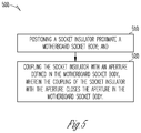
- FIG. 5 shows one example of a method 500 for manufacturing an electronic device, including one or more of the electronic devices described herein.
- the method 500 reference is made to one or more components, features, functions and steps previously described herein. Where convenient, reference is made to the components, features, steps and the like with reference numerals. The reference numerals provided are exemplary and are not exclusive. For instance, components, features, functions, steps and the like described in the method 500 include, but are not limited to, the corresponding numbered elements provided herein and other corresponding elements described herein (both numbered and unnumbered) as well as their equivalents.
- the method 500 can include at operation 510 positioning a socket insulator 150 proximate a motherboard socket body 110 .
- the method 500 can include at operation 520 coupling the socket insulator 150 with an aperture 140 defined in the motherboard socket body 110 .
- the coupling of the socket insulator 150 with the aperture 140 closes the aperture 140 in the motherboard socket body 110 .
- the method 500 may include coupling a processor 130 with the motherboard socket body 110 .
- the coupling of the processor 130 with the motherboard socket body 110 may correspondingly cover the aperture 140 in the motherboard socket body 110 .
- the method 500 may include positioning at least one capacitor (e.g., the processor electrical components 135 of FIG. 1 ), that may be coupled with the processor 130 , within the aperture 140 in the motherboard socket body 110 .
- the method 500 may include recessing the socket insulator 150 such that the socket insulator 150 is not coplanar with a mating surface of the motherboard socket body 110 .
- the method 500 may include applying an adhesive to either the socket insulator 150 or the motherboard socket body 110 .
- the adhesive may help couple the socket insulator 150 with the motherboard socket body 110 .
- the method 500 may include coupling the motherboard socket body 110 with a motherboard 120 .
- FIG. 6 illustrates a system level diagram, depicting an example of an electronic device (e.g., system) including the electronic device 100 , the socket body 110 , or the socket cavity insulator 150 , as described in the present disclosure.
- FIG. 6 is included to show an example of a higher level device application for the electronic device 100 , the socket body 110 , or the socket insulator 150 .
- system 600 includes, but is not limited to, a desktop computer, a laptop computer, a netbook, a tablet, a notebook computer, a personal digital assistant (PDA), a server, a workstation, a cellular telephone, a mobile computing device, a smart phone, an Internet appliance or any other type of computing device.
- system 600 is a system on a chip (SOC) system.
- SOC system on a chip
- processor 610 has one or more processor cores 612 and 612 N, where 612 N represents the Nth processor core inside processor 610 where N is a positive integer.
- system 600 includes multiple processors including 610 and 605 , where processor 605 has logic similar or identical to the logic of processor 610 .
- processing core 612 includes, but is not limited to, pre-fetch logic to fetch instructions, decode logic to decode the instructions, execution logic to execute instructions and the like.
- processor 610 has a cache memory 616 to cache instructions and/or data for system 600 . Cache memory 616 may be organized into a hierarchal structure including one or more levels of cache memory.
- processor 610 includes a memory controller 614 , which is operable to perform functions that enable the processor 610 to access and communicate with memory 630 that includes a volatile memory 632 and/or a non-volatile memory 634 .
- processor 610 is coupled with memory 630 and chipset 620 .
- Processor 610 may also be coupled to a wireless antenna 678 to communicate with any device configured to transmit and/or receive wireless signals.
- an interface for wireless antenna 678 operates in accordance with, but is not limited to, the IEEE 802.11 standard and its related family, Home Plug AV (HPAV), Ultra Wide Band (UWB), Bluetooth, WiMax, or any form of wireless communication protocol.
- volatile memory 632 includes, but is not limited to, Synchronous Dynamic Random Access Memory (SDRAM), Dynamic Random Access Memory (DRAM), RAMBUS Dynamic Random Access Memory (RDRAM), and/or any other type of random access memory device.
- Non-volatile memory 634 includes, but is not limited to, flash memory, phase change memory (PCM), read-only memory (ROM), electrically erasable programmable read-only memory (EEPROM), or any other type of non-volatile memory device.
- Memory 630 stores information and instructions to be executed by processor 610 .
- memory 630 may also store temporary variables or other intermediate information while processor 610 is executing instructions.
- chipset 620 connects with processor 610 via Point-to-Point (PtP or P-P) interfaces 617 and 622 .
- Chipset 620 enables processor 610 to connect to other elements in system 600 .
- interfaces 617 and 622 operate in accordance with a PtP communication protocol such as the Intel® QuickPath Interconnect (QPI) or the like. In other embodiments, a different interconnect may be used.
- PtP Point-to-Point
- QPI QuickPath Interconnect
- chipset 620 is operable to communicate with processor 610 , 605 N, display device 640 , and other devices, including a bus bridge 672 , a smart TV 676 , I/O devices 674 , nonvolatile memory 660 , a storage medium (such as one or more mass storage devices) 662 , a keyboard/mouse 664 , a network interface 666 , and various forms of consumer electronics 677 (such as a PDA, smart phone, tablet etc.), etc.
- chipset 620 couples with these devices through an interface 624 .
- Chipset 620 may also be coupled to a wireless antenna 678 to communicate with any device configured to transmit and/or receive wireless signals.
- Chipset 620 connects to display device 640 via interface 626 .
- Display 640 may be, for example, a liquid crystal display (LCD), a plasma display, cathode ray tube (CRT) display, or any other form of visual display device.
- processor 610 and chipset 620 are merged into a single SOC.
- chipset 620 connects to one or more buses 650 and 655 that interconnect various system elements, such as I/O devices 674 , nonvolatile memory 660 , storage medium 662 , a keyboard/mouse 664 , and network interface 666 .
- Buses 650 and 655 may be interconnected together via a bus bridge 672 .
- mass storage device 662 includes, but is not limited to, a solid state drive, a hard disk drive, a universal serial bus flash memory drive, or any other form of computer data storage medium.
- network interface 666 is implemented by any type of well-known network interface standard including, but not limited to, an Ethernet interface, a universal serial bus (USB) interface, a Peripheral Component Interconnect (PCI) Express interface, a wireless interface and/or any other suitable type of interface.
- the wireless interface operates in accordance with, but is not limited to, the IEEE 802.11 standard and its related family, Home Plug AV (HPAV), Ultra Wide Band (UWB), Bluetooth, WiMax, or any form of wireless communication protocol.
- modules shown in FIG. 6 are depicted as separate blocks within the system 600 , the functions performed by some of these blocks may be integrated within a single semiconductor circuit or may be implemented using two or more separate integrated circuits.
- cache memory 616 is depicted as a separate block within processor 610 , cache memory 616 (or selected aspects of 616 ) can be incorporated into processor core 612 .
- Aspect 1 may include or use subject matter (such as an apparatus, a system, a device, a method, a means for performing acts, or a device readable medium including instructions that, when performed by the device, may cause the device to perform acts, or an article of manufacture), such as may include or use an electronic device.
- the electronic device may include a motherboard socket body.
- the motherboard socket body may be adapted to couple with a processor.
- the motherboard socket body may define an aperture in the motherboard socket body.
- the electronic device may include a socket insulator.
- the socket insulator may be coupled with the aperture in the motherboard socket body.
- the socket insulator may include an insulator body.
- the insulator body may be sized and shaped to close the aperture in the motherboard socket body.
- Aspect 3 may include or use, or may optionally be combined with the subject matter of one or any combination of Aspects 1 or 2 to optionally include or use that a portion of the socket insulator can be biased toward the aperture, such as toward a wall of the aperture in the motherboard socket body.
- Aspect 4 may include or use, or may optionally be combined with the subject matter of one or any combination of Aspects 1 through 3 to optionally include or use a capacitor.
- the capacitor may be positioned within the aperture.
- the capacitor may be positioned on a first side of the socket insulator.
- Aspect 5 may include or use, or may optionally be combined with the subject matter of Aspect 4 to optionally include or use that a gap may exist between the first side of the socket insulator and the capacitor.
- Aspect 6 may include or use, or may optionally be combined with the subject matter of one or any combination of Aspects 4 or 5 to optionally include or use that the socket insulator may form a direct interface with the capacitor.
- Aspect 7 may include or use, or may optionally be combined with the subject matter of Aspect 6 to optionally include or use that a portion of the socket insulator may be adapted to deflect in response to forming a direct interface with the capacitor.
- Aspect 8 may include or use, or may optionally be combined with the subject matter of one or any combination of Aspects 1 through 7 to optionally include or use that the socket insulator may include an insulator coupling feature.
- the insulator coupling feature may be adapted to couple with a corresponding aperture coupling feature.
- Aspect 9 may include or use, or may optionally be combined with the subject matter of Aspect 8 to optionally include or use that the aperture coupling feature may be defined by a wall of the aperture in the motherboard socket body.
- Aspect 10 may include or use, or may optionally be combined with the subject matter of one or any combination of Aspects 1 through 9 to optionally include or use that the socket insulator may include a lip.
- the lip may be sized and shaped such that the lip may engage with a periphery of the aperture.
- Aspect 11 may include or use, or may optionally be combined with the subject matter of one or any combination of Aspects 1 through 10 to optionally include or use that the insulator body may include polyimides or polyester.
- Aspect 12 may include or use subject matter (such as an apparatus, a system, a device, a method, a means for performing acts, or a device readable medium including instructions that, when performed by the device, may cause the device to perform acts, or an article of manufacture), such as may include or use an electronic device.
- the electronic device may include a motherboard.
- the motherboard may include a motherboard socket body.
- the motherboard socket body may define an aperture in the motherboard socket body.
- the electronic device may include a processor.
- the processor may be coupled with the motherboard socket body.
- the motherboard socket body may cover the aperture in the motherboard socket body.
- the electronic device may include a socket insulator.
- the socket insulator may be coupled with the aperture in the motherboard socket body.
- the socket insulator may include an insulator body. The insulator body may be sized and shaped to close the aperture in the motherboard socket body.
- Aspect 13 may include or use, or may optionally be combined with the subject matter of Aspect 1, to optionally include or use that the motherboard may include a motherboard capacitor.
- the motherboard capacitor may be positioned on a first side of the socket insulator.
- the processor may include a processor capacitor.
- the processor capacitor may be positioned on a second side of the socket insulator.
- Aspect 14 may include or use, or may optionally be combined with the subject matter of Aspect 13 to optionally include or use that a gap may exist between the processor capacitor and the second side of the socket insulator.
- Aspect 15 may include or use, or may optionally be combined with the subject matter of one or any combination of Aspects 12 through 14 to optionally include or use that the insulator body may be compressed between the processor capacitor and the motherboard capacitor.
- Aspect 16 may include or use subject matter (such as an apparatus, a system, a device, a method, a means for performing acts, or a device readable medium including instructions that, when performed by the device, may cause the device to perform acts, or an article of manufacture), such as may include or use a method for manufacturing an electronic device.
- the method may include positioning a socket insulator proximate a motherboard socket body.
- the method may include coupling the socket insulator with an aperture defined in the motherboard socket body. The coupling of the socket insulator with the aperture may close the aperture in the motherboard socket body.
- Aspect 17 may include or use, or may optionally be combined with the subject matter of Aspect 16, to optionally include or use that the method may include coupling a processor with the motherboard socket body.
- the coupling of the processor with the motherboard socket body may correspondingly cover the aperture in the motherboard socket body.
- Aspect 18 may include or use, or may optionally be combined with the subject matter of one or any combination of Aspects 16 or 17 to optionally include or use that the method may include positioning at least one capacitor coupled with a processor within the aperture in the motherboard socket body.
- Aspect 19 may include or use, or may optionally be combined with the subject matter of one or any combination of Aspects 16 through 18 to optionally include or use that the method may include recessing the socket insulator such that the socket insulator is not coplanar with a mating surface of the motherboard socket body.
- Aspect 20 may include or use, or may optionally be combined with the subject matter of one or any combination of Aspects 16 through 19 to optionally include or use that the method may include applying an adhesive to either the socket insulator or the motherboard socket body.
- Aspect 21 may include or use, or may optionally be combined with the subject matter of one or any combination of Aspects 16 through 20 to optionally include or use that the method may include coupling the motherboard socket body with a motherboard.
- the terms “a” or “an” are used, as is common in patent documents, to include one or more than one, independent of any other instances or usages of “at least one” or “one or more.”
- the term “or” is used to refer to a nonexclusive or, such that “A or B” includes “A but not B,” “B but not A,” and “A and B,” unless otherwise indicated.
- Geometric terms such as “parallel”, “perpendicular”, “round”, or “square”, are not intended to require absolute mathematical precision, unless the context indicates otherwise. Instead, such geometric terms allow for variations due to manufacturing or equivalent functions. For example, if an element is described as “round” or “generally round,” a component that is not precisely circular (e.g., one that is slightly oblong or is a many-sided polygon) is still encompassed by this description.
- Method examples described herein may be machine or computer-implemented at least in part. Some examples may include a computer-readable medium or machine-readable medium encoded with instructions operable to configure an electronic device to perform methods as described in the above examples.
- An implementation of such methods may include code, such as microcode, assembly language code, a higher-level language code, or the like. Such code may include computer readable instructions for performing various methods. The code may form portions of computer program products. Further, in an example, the code may be tangibly stored on one or more volatile, non-transitory, or non-volatile tangible computer-readable media, such as during execution or at other times.
- Examples of these tangible computer-readable media may include, but are not limited to, hard disks, removable magnetic disks, removable optical disks (e.g., compact disks and digital video disks), magnetic cassettes, memory cards or sticks, random access memories (RAMs), read only memories (ROMs), and the like.
Landscapes
- Engineering & Computer Science (AREA)
- Microelectronics & Electronic Packaging (AREA)
- Theoretical Computer Science (AREA)
- Manufacturing & Machinery (AREA)
- Human Computer Interaction (AREA)
- Physics & Mathematics (AREA)
- General Engineering & Computer Science (AREA)
- General Physics & Mathematics (AREA)
- Connecting Device With Holders (AREA)
Abstract
Description
Claims (11)
Priority Applications (1)
| Application Number | Priority Date | Filing Date | Title |
|---|---|---|---|
| US15/941,427 US10729010B2 (en) | 2018-03-30 | 2018-03-30 | Socket cavity insulator |
Applications Claiming Priority (1)
| Application Number | Priority Date | Filing Date | Title |
|---|---|---|---|
| US15/941,427 US10729010B2 (en) | 2018-03-30 | 2018-03-30 | Socket cavity insulator |
Publications (2)
| Publication Number | Publication Date |
|---|---|
| US20190306984A1 US20190306984A1 (en) | 2019-10-03 |
| US10729010B2 true US10729010B2 (en) | 2020-07-28 |
Family
ID=68055833
Family Applications (1)
| Application Number | Title | Priority Date | Filing Date |
|---|---|---|---|
| US15/941,427 Expired - Fee Related US10729010B2 (en) | 2018-03-30 | 2018-03-30 | Socket cavity insulator |
Country Status (1)
| Country | Link |
|---|---|
| US (1) | US10729010B2 (en) |
Citations (5)
| Publication number | Priority date | Publication date | Assignee | Title |
|---|---|---|---|---|
| US6722896B2 (en) * | 2001-03-22 | 2004-04-20 | Molex Incorporated | Stitched LGA connector |
| US20060052011A1 (en) * | 2004-09-08 | 2006-03-09 | Advanced Interconnections Corporation | Double-pogo converter socket terminal |
| US7037115B2 (en) * | 2004-05-13 | 2006-05-02 | Intel Corporation | Attaching integrated circuits to printed circuit boards |
| US20080142962A1 (en) * | 2004-06-28 | 2008-06-19 | Intel Corporation | Integrated circuit packages, systems, and methods |
| US7578678B2 (en) * | 2004-10-25 | 2009-08-25 | Intel Corporation | Protected socket for integrated circuit devices |
-
2018
- 2018-03-30 US US15/941,427 patent/US10729010B2/en not_active Expired - Fee Related
Patent Citations (5)
| Publication number | Priority date | Publication date | Assignee | Title |
|---|---|---|---|---|
| US6722896B2 (en) * | 2001-03-22 | 2004-04-20 | Molex Incorporated | Stitched LGA connector |
| US7037115B2 (en) * | 2004-05-13 | 2006-05-02 | Intel Corporation | Attaching integrated circuits to printed circuit boards |
| US20080142962A1 (en) * | 2004-06-28 | 2008-06-19 | Intel Corporation | Integrated circuit packages, systems, and methods |
| US20060052011A1 (en) * | 2004-09-08 | 2006-03-09 | Advanced Interconnections Corporation | Double-pogo converter socket terminal |
| US7578678B2 (en) * | 2004-10-25 | 2009-08-25 | Intel Corporation | Protected socket for integrated circuit devices |
Also Published As
| Publication number | Publication date |
|---|---|
| US20190306984A1 (en) | 2019-10-03 |
Similar Documents
| Publication | Publication Date | Title |
|---|---|---|
| US12033953B2 (en) | Electronic device and crosstalk mitigating substrate | |
| US10504854B2 (en) | Through-stiffener inerconnects for package-on-package apparatus and methods of assembling same | |
| US10980129B2 (en) | Asymmetric electronic substrate and method of manufacture | |
| US11652071B2 (en) | Electronic device package including a capacitor | |
| US10847450B2 (en) | Compact wirebonding in stacked-chip system in package, and methods of making same | |
| US10535590B2 (en) | Multi-layer solder resists for semiconductor device package surfaces and methods of assembling same | |
| US11540395B2 (en) | Stacked-component placement in multiple-damascene printed wiring boards for semiconductor package substrates | |
| US11527484B2 (en) | Dielectric filler material in conductive material that functions as fiducial for an electronic device | |
| US20200153080A1 (en) | Antennas integrated into a printed circuit board | |
| US10729010B2 (en) | Socket cavity insulator | |
| US11037855B2 (en) | Contoured-on-heat-sink, wrapped printed wiring boards for system-in-package apparatus | |
| US10720393B2 (en) | Molded substrate package in fan-out wafer level package | |
| US20200083153A1 (en) | Electronic device including a lateral trace | |
| US11133261B2 (en) | Electronic device packaging | |
| WO2023114010A1 (en) | Liquid metal connection device and method | |
| US20180189217A1 (en) | Techniques for an extendable peripheral port | |
| US11049801B2 (en) | Encapsulated vertical interconnects for high-speed applications and methods of assembling same | |
| US20240006323A1 (en) | Interconnect bridge with similar channel lengths | |
| US20190355700A1 (en) | Techniques for windowed substrate integrated circuit packages | |
| US20220223487A1 (en) | Embedded component and methods of making the same | |
| US10785872B2 (en) | Package jumper interconnect | |
| US20190333854A1 (en) | Electronic chip with under-side power block | |
| US11495514B2 (en) | Bathtub integrated heat spreader with multiple thermal-interface material for integrated-circuit packages | |
| US20150140842A1 (en) | Receptacle connector | |
| EP4152383A2 (en) | Fiducial for an electronic device |
Legal Events
| Date | Code | Title | Description |
|---|---|---|---|
| FEPP | Fee payment procedure |
Free format text: ENTITY STATUS SET TO UNDISCOUNTED (ORIGINAL EVENT CODE: BIG.); ENTITY STATUS OF PATENT OWNER: LARGE ENTITY |
|
| AS | Assignment |
Owner name: INTEL CORPORATION, CALIFORNIA Free format text: ASSIGNMENT OF ASSIGNORS INTEREST;ASSIGNORS:WILLIS, DANIEL;GERBUS, DAN H;SIGNING DATES FROM 20180405 TO 20180406;REEL/FRAME:045626/0369 |
|
| STPP | Information on status: patent application and granting procedure in general |
Free format text: FINAL REJECTION MAILED |
|
| STPP | Information on status: patent application and granting procedure in general |
Free format text: RESPONSE AFTER FINAL ACTION FORWARDED TO EXAMINER |
|
| STPP | Information on status: patent application and granting procedure in general |
Free format text: NOTICE OF ALLOWANCE MAILED -- APPLICATION RECEIVED IN OFFICE OF PUBLICATIONS |
|
| STPP | Information on status: patent application and granting procedure in general |
Free format text: PUBLICATIONS -- ISSUE FEE PAYMENT VERIFIED |
|
| STCF | Information on status: patent grant |
Free format text: PATENTED CASE |
|
| FEPP | Fee payment procedure |
Free format text: MAINTENANCE FEE REMINDER MAILED (ORIGINAL EVENT CODE: REM.); ENTITY STATUS OF PATENT OWNER: LARGE ENTITY |
|
| LAPS | Lapse for failure to pay maintenance fees |
Free format text: PATENT EXPIRED FOR FAILURE TO PAY MAINTENANCE FEES (ORIGINAL EVENT CODE: EXP.); ENTITY STATUS OF PATENT OWNER: LARGE ENTITY |
|
| STCH | Information on status: patent discontinuation |
Free format text: PATENT EXPIRED DUE TO NONPAYMENT OF MAINTENANCE FEES UNDER 37 CFR 1.362 |
|
| FP | Lapsed due to failure to pay maintenance fee |
Effective date: 20240728 |