US10726890B2 - Resistive memory apparatus and operating method thereof - Google Patents
Resistive memory apparatus and operating method thereof Download PDFInfo
- Publication number
- US10726890B2 US10726890B2 US16/177,460 US201816177460A US10726890B2 US 10726890 B2 US10726890 B2 US 10726890B2 US 201816177460 A US201816177460 A US 201816177460A US 10726890 B2 US10726890 B2 US 10726890B2
- Authority
- US
- United States
- Prior art keywords
- signal transmission
- terminal
- voltage
- memory cells
- transmission path
- Prior art date
- Legal status (The legal status is an assumption and is not a legal conclusion. Google has not performed a legal analysis and makes no representation as to the accuracy of the status listed.)
- Active
Links
- 238000011017 operating method Methods 0.000 title claims abstract description 21
- 230000008054 signal transmission Effects 0.000 claims abstract description 97
- 238000000034 method Methods 0.000 claims description 39
- 238000010586 diagram Methods 0.000 description 6
- 229910052760 oxygen Inorganic materials 0.000 description 5
- 239000001301 oxygen Substances 0.000 description 5
- 238000012360 testing method Methods 0.000 description 4
- 230000008901 benefit Effects 0.000 description 3
- -1 oxygen ions Chemical class 0.000 description 3
- QVGXLLKOCUKJST-UHFFFAOYSA-N atomic oxygen Chemical compound [O] QVGXLLKOCUKJST-UHFFFAOYSA-N 0.000 description 2
- 230000000694 effects Effects 0.000 description 2
- 238000012986 modification Methods 0.000 description 2
- 230000004048 modification Effects 0.000 description 2
- 230000000295 complement effect Effects 0.000 description 1
- 238000004519 manufacturing process Methods 0.000 description 1
- 230000003071 parasitic effect Effects 0.000 description 1
- 238000012545 processing Methods 0.000 description 1
- 239000004065 semiconductor Substances 0.000 description 1
Images


Classifications
-
- G—PHYSICS
- G11—INFORMATION STORAGE
- G11C—STATIC STORES
- G11C11/00—Digital stores characterised by the use of particular electric or magnetic storage elements; Storage elements therefor
-
- G—PHYSICS
- G11—INFORMATION STORAGE
- G11C—STATIC STORES
- G11C13/00—Digital stores characterised by the use of storage elements not covered by groups G11C11/00, G11C23/00, or G11C25/00
- G11C13/0002—Digital stores characterised by the use of storage elements not covered by groups G11C11/00, G11C23/00, or G11C25/00 using resistive RAM [RRAM] elements
- G11C13/0021—Auxiliary circuits
- G11C13/0069—Writing or programming circuits or methods
-
- G—PHYSICS
- G11—INFORMATION STORAGE
- G11C—STATIC STORES
- G11C13/00—Digital stores characterised by the use of storage elements not covered by groups G11C11/00, G11C23/00, or G11C25/00
- G11C13/0002—Digital stores characterised by the use of storage elements not covered by groups G11C11/00, G11C23/00, or G11C25/00 using resistive RAM [RRAM] elements
- G11C13/0021—Auxiliary circuits
- G11C13/0023—Address circuits or decoders
- G11C13/0026—Bit-line or column circuits
-
- G—PHYSICS
- G11—INFORMATION STORAGE
- G11C—STATIC STORES
- G11C13/00—Digital stores characterised by the use of storage elements not covered by groups G11C11/00, G11C23/00, or G11C25/00
- G11C13/0002—Digital stores characterised by the use of storage elements not covered by groups G11C11/00, G11C23/00, or G11C25/00 using resistive RAM [RRAM] elements
- G11C13/0021—Auxiliary circuits
- G11C13/003—Cell access
-
- G—PHYSICS
- G11—INFORMATION STORAGE
- G11C—STATIC STORES
- G11C13/00—Digital stores characterised by the use of storage elements not covered by groups G11C11/00, G11C23/00, or G11C25/00
- G11C13/0002—Digital stores characterised by the use of storage elements not covered by groups G11C11/00, G11C23/00, or G11C25/00 using resistive RAM [RRAM] elements
- G11C13/0021—Auxiliary circuits
- G11C13/0033—Disturbance prevention or evaluation; Refreshing of disturbed memory data
-
- G—PHYSICS
- G11—INFORMATION STORAGE
- G11C—STATIC STORES
- G11C13/00—Digital stores characterised by the use of storage elements not covered by groups G11C11/00, G11C23/00, or G11C25/00
- G11C13/0002—Digital stores characterised by the use of storage elements not covered by groups G11C11/00, G11C23/00, or G11C25/00 using resistive RAM [RRAM] elements
- G11C13/0021—Auxiliary circuits
- G11C13/0038—Power supply circuits
-
- G—PHYSICS
- G11—INFORMATION STORAGE
- G11C—STATIC STORES
- G11C13/00—Digital stores characterised by the use of storage elements not covered by groups G11C11/00, G11C23/00, or G11C25/00
- G11C13/0002—Digital stores characterised by the use of storage elements not covered by groups G11C11/00, G11C23/00, or G11C25/00 using resistive RAM [RRAM] elements
- G11C13/0021—Auxiliary circuits
- G11C13/004—Reading or sensing circuits or methods
-
- G—PHYSICS
- G11—INFORMATION STORAGE
- G11C—STATIC STORES
- G11C13/00—Digital stores characterised by the use of storage elements not covered by groups G11C11/00, G11C23/00, or G11C25/00
- G11C13/0002—Digital stores characterised by the use of storage elements not covered by groups G11C11/00, G11C23/00, or G11C25/00 using resistive RAM [RRAM] elements
- G11C13/0021—Auxiliary circuits
- G11C13/0097—Erasing, e.g. resetting, circuits or methods
-
- G—PHYSICS
- G11—INFORMATION STORAGE
- G11C—STATIC STORES
- G11C13/00—Digital stores characterised by the use of storage elements not covered by groups G11C11/00, G11C23/00, or G11C25/00
- G11C13/0002—Digital stores characterised by the use of storage elements not covered by groups G11C11/00, G11C23/00, or G11C25/00 using resistive RAM [RRAM] elements
- G11C13/0021—Auxiliary circuits
- G11C13/0069—Writing or programming circuits or methods
- G11C2013/0073—Write using bi-directional cell biasing
-
- G—PHYSICS
- G11—INFORMATION STORAGE
- G11C—STATIC STORES
- G11C13/00—Digital stores characterised by the use of storage elements not covered by groups G11C11/00, G11C23/00, or G11C25/00
- G11C13/0002—Digital stores characterised by the use of storage elements not covered by groups G11C11/00, G11C23/00, or G11C25/00 using resistive RAM [RRAM] elements
- G11C13/0021—Auxiliary circuits
- G11C13/0069—Writing or programming circuits or methods
- G11C2013/0083—Write to perform initialising, forming process, electro forming or conditioning
-
- G—PHYSICS
- G11—INFORMATION STORAGE
- G11C—STATIC STORES
- G11C2213/00—Indexing scheme relating to G11C13/00 for features not covered by this group
- G11C2213/70—Resistive array aspects
- G11C2213/79—Array wherein the access device being a transistor
-
- G—PHYSICS
- G11—INFORMATION STORAGE
- G11C—STATIC STORES
- G11C2213/00—Indexing scheme relating to G11C13/00 for features not covered by this group
- G11C2213/70—Resistive array aspects
- G11C2213/82—Array having, for accessing a cell, a word line, a bit line and a plate or source line receiving different potentials
Definitions
- the invention relates to a memory apparatus and an operating method thereof, and more particularly, to a resistive memory apparatus and an operating method thereof.
- the resistive memory e.g., resistive random access memory (RRAM)
- RRAM resistive random access memory
- the conventional resistive memory usually includes a top electrode and a bottom electrode disposed opposite to each other, and a dielectric layer located between the top electrode and the bottom electrode.
- a forming procedure for a current path needs be completed.
- the forming procedure includes applying a bias (e.g., a positive bias) to the resistive memory so current flows from the top electrode to the bottom electrode and oxygen vacancy and oxygen ions can be generated in the dielectric layer to form the current path (also called as a filament), such that the resistive memory is changed from high resistance state (HRS) to low resistance state (LRS).
- a bias e.g., a positive bias
- a diameter of a portion near the top electrode is smaller than a diameter of a portion near the bottom electrode.
- processes of resetting or setting the resistive memory may be performed so the resistive memory can switch between HRS and LRS to store data.
- a reverse bias with opposite polarity to a bias in the process of setting is applied to the resistive memory such that current flows from the bottom electrode to the top electrode.
- oxygen vacancy is combined with some of oxygen ions at the portion near the top electrode to interrupt the current path such that the filament is cut off at the portion near the top electrode.
- the bias with identical polarity to the bias for forming the filament is applied to the resistive memory such that current flows from the top electrode to the bottom electrode. At this time, oxygen ions at the portion near the top electrode are released such that the filament is re-formed at the portion near the top electrode.
- the memory cells at different locations may have different distances with respect to the voltage source. The distances can derive a parasitic IR drop effect. After the forming procedure and/or the initial reset operation are completed, the memory cells at the different locations will show different characteristics due to the IR drop effect, resulting in uneven quality of the memory cell array overall, thereby reducing reliability for reading and writing the memory cells.
- the invention is directed to a resistive memory apparatus and an operating method thereof.
- Such operating method can be automatically performed and can improve reliability for reading or wiring memory cells.
- the resistive memory apparatus of the invention includes a memory cell array and a voltage selector circuit.
- the memory cell array includes a plurality of memory cells.
- the voltage selector circuit is coupled to the memory cell array.
- the voltage selector circuit performs a voltage applying operation on the memory cells via a plurality of different signal transmission paths. Each of the signal transmission paths passes one of the memory cells. IR drops of two of the signal transmission paths are substantially identical, and signal transmission directions thereof are different.
- the operating method of the resistive memory apparatus of the invention includes multiple steps.
- the resistive memory apparatus includes M memory cells.
- a first step is to perform a voltage applying operation on an Nth memory cell of the M memory cells via a first signal transmission path, wherein the first signal transmission path passes the Nth memory cell, and N ⁇ M where M and N are positive integers;
- a second step is to perform the voltage applying operation on a Kth memory cell of the M memory cells via a second signal transmission path, wherein the second signal transmission path passes the Kth memory cell, and K ⁇ M where K is a positive integer;
- a third step is to repeatedly perform the first step and the second step until the voltage applying operation is completed for all of the M memory cells.
- An IR drop of the first signal transmission path is substantially identical to an IR drop of the second signal transmission path, and a signal transmission direction of the first signal transmission path is different from a signal transmission direction of the second signal transmission path.
- FIG. 1 illustrates a schematic diagram of a resistive memory apparatus in an embodiment of the invention.
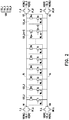
- FIG. 2 illustrates a schematic diagram of a memory cell array and a voltage selector circuit in the embodiment of FIG. 1 .
- FIG. 3A , FIG. 3B , FIG. 3C and FIG. 3D illustrate schematic diagrams of a voltage applying operation performed on the memory cells by the voltage selector circuit in the embodiment of FIG. 2 .
- FIG. 4 illustrates a flowchart of an operating method of a resistive memory apparatus in an embodiment of the invention.
- FIG. 5 illustrates a flowchart of an operating method of a resistive memory apparatus in another embodiment of the invention.
- Couple used throughout the specification (including claims) may refer to any direct or indirect electrical connection means. Further, there is no sequential relationship between each of ordinal numbers in the specification or the claims, such as “first”, “second”, “third”, etc.
- FIG. 1 illustrates a schematic diagram of a resistive memory apparatus in an embodiment of the invention.
- FIG. 2 illustrates a schematic diagram of a memory cell array and a voltage selector circuit in the embodiment of FIG. 1 .
- a resistive memory apparatus 100 of the present embodiment includes a memory controller 110 and a memory cell array 120 .
- the memory controller 110 is configured to control overall operations of the memory cell array 120 including procedures or operations such as a forming procedure, an initial reset operation, a reset operation, a set operation, a write operation and a read operation, etc., and enough teaching, suggestion, and implementation illustration regarding a control method of the above may be obtained with reference to common knowledge in the related art.
- the memory cell array 120 includes a source line SL, a bit line BL, a plurality of word lines WL_ 1 to WL_m and a plurality of memory cells 122 _ 1 to 122 _ m .
- the memory cell array 120 includes M memory cells, where M is a positive integer.
- Each of the memory cells includes a variable resistance element and a switch element.
- the memory cell 122 _ 1 includes a variable resistance element R 1 and a switch element T 1
- the memory cell 122 _ m includes a variable resistance element Rm and a switch element Tm, and structures of the remaining memory cells may be derived likewise.
- the memory cell array 120 includes a first terminal N 1 , a second terminal N 2 , a third terminal N 3 and a fourth terminal N 4 .
- the voltage selector circuit 130 is configured to couple the first terminal N 1 , the second terminal N 2 , the third terminal N 3 and the fourth terminal N 4 to predetermined voltages, so as to perform a voltage applying operation on the memory cells 122 _ 1 to 122 _ m .
- the voltage selector circuit 130 may be disposed on the memory cell array 120 or other circuit blocks in the resistive memory apparatus 100 , and a disposing location of the voltage selector circuit 130 is not particularly limited in the invention.
- a first terminal of the switch element of each of the memory cells 122 _ 1 to 122 _ m is coupled to the first terminal N 1 and the third terminal N 3 via the bit line BL.
- a second terminal of the switch element of each of the memory cells 122 _ 1 to 122 _ m is coupled to the second terminal N 2 and the fourth terminal N 4 via the source line SL.
- a control terminal of the switch element of each of the memory cells 122 _ 1 to 122 _ m is coupled to corresponding one of the word lines WL_ 1 to WL_m.
- the voltage selector circuit 130 includes a first voltage selector 132 _ 1 , a second voltage selector 132 _ 2 , a third voltage selector 132 _ 3 and a fourth voltage selector 132 _ 4 .
- the first voltage selector 132 _ 1 couples the first terminal N 1 of the memory cell array 120 to a first voltage V 1 or a second voltage V 2 according to control signals F_L and bF_L.
- the second voltage selector 132 _ 2 couples the second terminal N 2 of the memory cell array 120 to a third voltage V 3 or a fourth voltage V 4 according to control signals R_R and bR_R.
- the third voltage selector 132 _ 3 couples the third terminal N 3 of the memory cell array 120 to the first voltage V 1 or the second voltage V 2 according to control signals F_R and bF_R.
- the fourth voltage selector 132 _ 4 couples the fourth terminal N 4 of the memory cell array 120 to the third voltage V 3 or the fourth voltage V 4 according to control signals R_L and bR_L. In this way, when the voltage applying operation is performed, the first voltage V 1 , the second voltage V 2 , the third voltage V 3 and the fourth voltage V 4 may be selected and applied to the corresponding memory cells.
- control signals F_L, bF_L, R_R, bR_R, F_R, bF_R, R_L and bR_L may be outputted by an additionally disposed Y-multiplexer (abbr. Y-MUX, which is not illustrated) and configured to control output voltages of the first voltage selector 132 _ 1 , the second voltage selector 132 _ 2 , the third voltage selector 132 _ 3 and the fourth voltage selector 132 _ 4 .
- Y-MUX Y-multiplexer
- the first voltage V 1 is, for example, a bit line voltage VBL
- the second voltage V 2 and the third voltage V 3 are, for example, a ground voltage (0 V)
- the fourth voltage V 4 is, for example, a source line voltage VSL.
- Implementation of the voltage selector circuit 130 and voltage values of the first voltage V 1 , the second voltage V 2 , the third voltage V 3 and the fourth voltage V 4 are not particularly limited in the invention.
- the voltage selector circuit 130 performs the voltage applying operation on the memory cells 122 _ 1 to 122 _ m via a plurality of different signal transmission paths. Each of the signal transmission paths includes one memory cell of the memory cells 122 _ 1 to 122 _ m .
- FIG. 3A to FIG. 3D illustrate schematic diagrams of a voltage applying operation performed on the memory cells by the voltage selector circuit in the embodiment of FIG. 2 .
- FIG. 4 illustrates a flowchart of an operating method of a resistive memory apparatus in an embodiment of the invention.
- step S 100 the voltage selector circuit 130 performs the voltage applying operation on an Nth memory cell via a first signal transmission path IR 1 _ 1 , as shown in FIG. 3A , where N is a positive integer less than M (N ⁇ M).
- step S 110 the voltage selector circuit 130 performs the voltage applying operation on a Kth memory cell via a second signal transmission path IR 2 _ 1 , as shown in FIG. 3B , where K is a positive integer less than or equal M (K ⁇ M).
- K is a positive integer less than or equal M (K ⁇ M).
- the first signal transmission path IR 1 _ 1 and the second signal transmission path IR 2 _ 1 have substantially identical IR drops and different signal transmission directions.
- the first signal transmission path IR 1 _ 1 is located between the first terminal N 1 and the second terminal N 2 , and when the switch element T 1 is turned on, a current signal is transmitted from the first terminal N 1 passing through the variable resistance element R 1 and the switch element T 1 to the second terminal N 2 .
- the first terminal of the switch element T 1 is coupled to the first voltage V 1 via the variable resistance element R 1
- the second terminal is coupled to the third voltage V 3 .
- the second signal transmission path IR 2 _ 1 is located between the third terminal N 3 and the fourth terminal N 4 , and when the switch element Tm is turned on, a current signal is transmitted from the third terminal N 3 passing through the variable resistance element Rm and the switch element Tm to the fourth terminal N 4 . At this time, the first terminal of the switch element Tm is coupled to the first voltage V 1 via the variable resistance element Rm, and the second terminal is coupled to the third voltage V 3 .
- the IR drop of the first signal transmission path IR 1 _ 1 is substantially identical to the IR drop of the second signal transmission path IR 2 _ 1 , and the signal transmission direction of the first signal transmission path IR 1 _ 1 is different from the signal transmission direction of the second signal transmission path IR 2 _ 1 .
- the voltage selector circuit 130 performs the voltage applying operation on the 1023rd memory cell.
- an IR drop of the first signal transmission path IR 1 _ 2 is substantially identical to an IR drop of the second signal transmission path IR 2 _ 2 , and a signal transmission direction of the first signal transmission path IR 1 _ 2 is different from a signal transmission direction of the second signal transmission path IR 2 _ 2 .
- the voltage applying operation performed on the remaining memory cells by the voltage selector circuit 130 may be derived from the content disclosed above.
- step S 120 if the voltage applying operation is completed for all of the memory cells, the operating method ends. That is to say, the voltage selector circuit 130 repeatedly performs steps S 100 and S 110 until the voltage applying operation is completed for all of the M memory cells.
- step S 120 may be performed by, for example, the memory controller 110 so whether or not the voltage selector circuit 130 repeatedly performs the steps S 100 and S 110 to complete the voltage applying operation can be controlled by the memory controller 110 .
- the first signal transmission path refers to, for example, a signal transmission path between the first terminal N 1 and the second terminal N 2 with a signal thereon (e.g., the current signal) transmitted from the first terminal N 1 to the second terminal N 2 .
- the second signal transmission path refers to, for example, a signal transmission path between the third terminal N 3 and the fourth terminal N 4 with a signal thereon (e.g., the current signal) transmitted from the third terminal N 3 to the fourth terminal N 4 .
- the switch element of one of the memory cells is turned on, and the switch elements of the remaining memory cells are not turned on.
- the switch element T 1 of the memory cell 122 _ 1 is turned on
- the switch elements of the remaining memory cells 122 _ 2 to 122 _ m are not turned on.
- the switch element Tm of the memory cell 122 _ m is turned on, the switch elements of the remaining memory cells 122 _ 1 to 122 _(m ⁇ 1) are not turned on.
- On-states of the switch elements T 1 to Tm may be controlled by a word line decoder, and enough teaching, suggestion, and implementation illustration regarding a control method of the above may be obtained with reference to common knowledge in the related art.
- a mark H indicates that the control signal of the switch element is at high level such that the switch element is turned on
- a mark L indicates that the control signal of the switch element is at low level such that the switch element is not turned on.
- each two of the signal transmission paths are paired up into a group of the signal transmission paths, and each group of the signal transmission paths has substantially identical IR drops and different signal transmission directions.
- the first signal transmission path IR 1 _ 1 and the second signal transmission path IR 2 _ 1 are paired into one group, and both signal transmission paths have the substantially identical IR drops and the different signal transmission directions.
- the first signal transmission path IR 1 _ 2 and the second signal transmission path IR 2 _ 2 are paired into one group, and both signal transmission paths have the substantially identical IR drops and the different signal transmission directions. Descriptions for the rest of the signal transmission paths may be deduced by analogy.
- the phenomenon of uneven voltage supply on the memory cells caused by the IR drops may be mitigated so as to improve reliability of the memory cells during reading and write operation.
- the voltage applying operation includes, for example, the procedures or operations such as the forming procedure, the initial reset operation, the reset operation, the write operation or the read operation.
- the voltage applying operation is, for example, the forming procedure.
- the first voltage V 1 (the bit line voltage VBL) may be set to 4 V
- the fourth voltage V 4 (the source line voltage VSL) may be set to 0 V.
- the voltage applying operation is, for example, the initial reset operation.
- the first voltage V 1 (the bit line voltage VBL) may be set to 0 V
- the fourth voltage V 4 (the source line voltage VSL) may be set to +2 to +3.5 V.
- the voltage applying operation is, for example, the reset operation.
- the first voltage V 1 (the bit line voltage VBL) may be set to 0 V
- the fourth voltage V 4 (the source line voltage VSL) may be set to +2 to +3.5 V.
- the voltage applying operation is, for example, the set operation.
- the first voltage V 1 (the bit line voltage VBL) may be set to +1.5 to +3.5 V
- the fourth voltage V 4 (the source line voltage VSL) may be set to 0 V.
- the voltage values of each voltage in the procedures or operations described above are merely illustrative description rather than limitations to the invention.
- the voltage applying operation may also be automatically performed.
- the voltage selector circuit 130 can automatically perform the voltage applying operation on the memory cells 122 _ 1 to 122 _ m according to an input command. For example, clients or manufacturers (before shipping) may give an automatically executed command so the voltage selector circuit 130 can automatically perform the forming procedure and/or the initial reset operation in order to reduce the test cost.
- the voltage selector circuit 130 can automatically perform the voltage applying operation on the memory cells 122 _ 1 to 122 _ m after a power up procedure. For example, clients or manufacturers (before shipping) may set the voltage selector circuit 130 to automatically perform the forming procedure and/or the initial reset operation after the power up procedure is performed for the first time in order to reduce the test cost.
- FIG. 5 illustrates a flowchart of an operating method of a resistive memory apparatus in another embodiment of the invention.
- the operating method of the resistive memory apparatus is to, for example, perform the forming procedure and/or the initial reset operation on the memory cells 122 _ 1 to 122 _ m .
- step S 200 a power up procedure is performed on the resistive memory apparatus 100 for the first time.
- step S 210 the resistive memory apparatus 100 enters a test mode of a forming procedure and/or an initial reset operation.
- the memory controller 110 sets the forming procedure and/or the initial reset operation to be performed starting with the memory cells 122 _ 1 and 122 _ m in sequence.
- step S 230 the voltage selector circuit 130 performs a voltage applying operation on an Nth memory cell of M memory cells via a first signal transmission path. Subsequently, in step S 240 , the voltage selector circuit 130 performs the voltage applying operation on a Kth memory cell of the M memory cells via a second signal transmission path.
- an IR drop of the first signal transmission path is substantially identical to an IR drop of the second signal transmission path, and a signal transmission direction of the first signal transmission path is different from a signal transmission direction of the second signal transmission path.
- step S 230 to step S 250 are repeated performed in the operating method of the resistive memory apparatus until the forming procedure and/or the initial reset operation are completed for all of the M memory cells, as shown by a loop of step S 230 to S 250 .
- the loop of step S 230 to S 250 is performed 512 times in the operating method.
- the first voltage V 1 (the bit line voltage VBL) may be set to 4 V and the fourth voltage V 4 (the source line voltage VSL) may be set to 0 V in the forming procedure.
- the first voltage V 1 (the bit line voltage VBL) may be set to 0 V and the fourth voltage V 4 (the source line voltage VSL) may be set to +2 to +3.5 V in the initial reset operation.
- the voltage selector circuit 130 when the voltage selector circuit 130 performs both the forming procedure and the initial reset operation on the memory cells, the voltage selector circuit 130 can perform the forming procedure on a target memory cell first before performing the initial reset operation. Taking the memory cells 122 _ 1 and 122 _ m for example, the voltage selector circuit 130 first performs the forming procedure on the memory cell 122 _ 1 before performing the initial reset operation. Next, the voltage selector circuit 130 then performs the forming procedure and the initial reset operation on the memory cell 122 _ m in sequence.
- the voltage applying operation includes the procedures or operations such as the forming procedure, the initial reset operation, the reset operation, the write operation or the read operation.
- the procedures or operations such as the forming procedure, the initial reset operation, the reset operation, the write operation or the read operation.
Landscapes
- Engineering & Computer Science (AREA)
- Computer Hardware Design (AREA)
- Semiconductor Memories (AREA)
Abstract
Description
Claims (13)
Applications Claiming Priority (3)
| Application Number | Priority Date | Filing Date | Title |
|---|---|---|---|
| CN201711264932 | 2017-12-05 | ||
| CN201711264932.7 | 2017-12-05 | ||
| CN201711264932.7A CN109872749B (en) | 2017-12-05 | 2017-12-05 | Resistive memory device and method of operation |
Publications (2)
| Publication Number | Publication Date |
|---|---|
| US20190172535A1 US20190172535A1 (en) | 2019-06-06 |
| US10726890B2 true US10726890B2 (en) | 2020-07-28 |
Family
ID=66658509
Family Applications (1)
| Application Number | Title | Priority Date | Filing Date |
|---|---|---|---|
| US16/177,460 Active US10726890B2 (en) | 2017-12-05 | 2018-11-01 | Resistive memory apparatus and operating method thereof |
Country Status (2)
| Country | Link |
|---|---|
| US (1) | US10726890B2 (en) |
| CN (1) | CN109872749B (en) |
Families Citing this family (1)
| Publication number | Priority date | Publication date | Assignee | Title |
|---|---|---|---|---|
| CN113628651B (en) * | 2020-05-06 | 2023-12-08 | 华邦电子股份有限公司 | Resistive memory storage device and operation method thereof |
Citations (8)
| Publication number | Priority date | Publication date | Assignee | Title |
|---|---|---|---|---|
| US20070008786A1 (en) * | 2005-07-11 | 2007-01-11 | Scheuerlein Roy E | Apparatus and method for reading an array of nonvolatile memory cells including switchable resistor memory elements |
| US8279654B2 (en) * | 2009-04-15 | 2012-10-02 | Sony Corporation | Resistance change memory device and operation method of the same |
| US8750043B2 (en) | 2012-08-16 | 2014-06-10 | Winbond Electronics Corp. | Data storage device and control method for non-volatile memory |
| CN103854693A (en) | 2012-11-29 | 2014-06-11 | 台湾积体电路制造股份有限公司 | Magnetoresistive random access memory (mram) differential bit cell and method of use |
| US9058872B2 (en) | 2013-01-31 | 2015-06-16 | Taiwan Semiconductor Manufacturing Company, Ltd. | Resistance-based random access memory |
| CN105097020A (en) | 2014-05-19 | 2015-11-25 | 旺宏电子股份有限公司 | Resistive memory and method of operation thereof |
| US20160133836A1 (en) * | 2014-11-11 | 2016-05-12 | Sandisk 3D Llc | High endurance non-volatile storage |
| US20160240250A1 (en) | 2015-02-17 | 2016-08-18 | Samsung Electronics Co., Ltd. | Resistive memory device, resistive memory system, and method of operating the resistive memory system |
Family Cites Families (5)
| Publication number | Priority date | Publication date | Assignee | Title |
|---|---|---|---|---|
| DE60223161T2 (en) * | 2001-06-20 | 2008-08-07 | Qimonda Ag | POWER SOURCE AND DRAIN ARRANGEMENT FOR MAGNETORESITIVE STORAGE |
| JP2007280458A (en) * | 2006-04-04 | 2007-10-25 | Toshiba Corp | Reference voltage generation circuit |
| JP5127665B2 (en) * | 2008-10-23 | 2013-01-23 | 株式会社東芝 | Semiconductor memory device |
| JP2012204404A (en) * | 2011-03-23 | 2012-10-22 | Toshiba Corp | Resistance change nonvolatile semiconductor memory device |
| US9865605B2 (en) * | 2016-01-14 | 2018-01-09 | Taiwan Semiconductor Manufacturing Company, Ltd. | Memory circuit having resistive device coupled with supply voltage line |
-
2017
- 2017-12-05 CN CN201711264932.7A patent/CN109872749B/en active Active
-
2018
- 2018-11-01 US US16/177,460 patent/US10726890B2/en active Active
Patent Citations (8)
| Publication number | Priority date | Publication date | Assignee | Title |
|---|---|---|---|---|
| US20070008786A1 (en) * | 2005-07-11 | 2007-01-11 | Scheuerlein Roy E | Apparatus and method for reading an array of nonvolatile memory cells including switchable resistor memory elements |
| US8279654B2 (en) * | 2009-04-15 | 2012-10-02 | Sony Corporation | Resistance change memory device and operation method of the same |
| US8750043B2 (en) | 2012-08-16 | 2014-06-10 | Winbond Electronics Corp. | Data storage device and control method for non-volatile memory |
| CN103854693A (en) | 2012-11-29 | 2014-06-11 | 台湾积体电路制造股份有限公司 | Magnetoresistive random access memory (mram) differential bit cell and method of use |
| US9058872B2 (en) | 2013-01-31 | 2015-06-16 | Taiwan Semiconductor Manufacturing Company, Ltd. | Resistance-based random access memory |
| CN105097020A (en) | 2014-05-19 | 2015-11-25 | 旺宏电子股份有限公司 | Resistive memory and method of operation thereof |
| US20160133836A1 (en) * | 2014-11-11 | 2016-05-12 | Sandisk 3D Llc | High endurance non-volatile storage |
| US20160240250A1 (en) | 2015-02-17 | 2016-08-18 | Samsung Electronics Co., Ltd. | Resistive memory device, resistive memory system, and method of operating the resistive memory system |
Also Published As
| Publication number | Publication date |
|---|---|
| US20190172535A1 (en) | 2019-06-06 |
| CN109872749A (en) | 2019-06-11 |
| CN109872749B (en) | 2020-12-01 |
Similar Documents
| Publication | Publication Date | Title |
|---|---|---|
| US8780617B2 (en) | Semiconductor memory device and method of performing burn-in test on the same | |
| US9343175B2 (en) | Fuse data reading circuit having multiple reading modes and related devices, systems and methods | |
| TWI581266B (en) | Array structure of resistive random-access memory | |
| US10388372B2 (en) | 1T-1R architecture for resistive random access memory | |
| US9405615B2 (en) | Method of operating nonvolatile memory device comprising resistance material | |
| US9627060B2 (en) | Memory circuit and method of programming memory circuit | |
| US9424914B2 (en) | Resistive memory apparatus and memory cell thereof | |
| US20200043566A1 (en) | Semiconductor device | |
| TWI746173B (en) | Resistive memory with self-termination control function and self-termination control method | |
| US20170069358A1 (en) | Memory device and method of operation thereof | |
| US9899078B2 (en) | Resistive random access memory with high-reliability and manufacturing and control methods thereof | |
| CN104733611B (en) | Resistive memory device and memory cell thereof | |
| US10354724B2 (en) | Methods and apparatus for programming barrier modulated memory cells | |
| US10726890B2 (en) | Resistive memory apparatus and operating method thereof | |
| CN107633857B (en) | Memory device and stress testing method thereof | |
| US20160148686A1 (en) | Memory cell array of resistive random-access memories | |
| JP5715306B2 (en) | Snapback detection at tile level using coupling capacitors in crosspoint arrays | |
| JP2015156248A (en) | Snapback detection at tile level using coupling capacitors in crosspoint arrays | |
| US10490272B2 (en) | Operating method of resistive memory element | |
| US9466375B1 (en) | Memory device and programming method thereof | |
| JPWO2013128854A1 (en) | Nonvolatile semiconductor memory device | |
| US20160111151A1 (en) | Resistance variable memory apparatus, read/write circuit unit and operation method thereof | |
| TWI612533B (en) | Low power memory device | |
| CN204667887U (en) | Memory device | |
| TWI645403B (en) | Resistive memory apparatus and operating method thereof |
Legal Events
| Date | Code | Title | Description |
|---|---|---|---|
| FEPP | Fee payment procedure |
Free format text: ENTITY STATUS SET TO UNDISCOUNTED (ORIGINAL EVENT CODE: BIG.); ENTITY STATUS OF PATENT OWNER: LARGE ENTITY |
|
| AS | Assignment |
Owner name: WINBOND ELECTRONICS CORP., TAIWAN Free format text: ASSIGNMENT OF ASSIGNORS INTEREST;ASSIGNORS:LIN, LIH-WEI;CHUANG, YU-CHENG;LEE, SUNG-YI;REEL/FRAME:047427/0866 Effective date: 20181030 |
|
| STPP | Information on status: patent application and granting procedure in general |
Free format text: DOCKETED NEW CASE - READY FOR EXAMINATION |
|
| STPP | Information on status: patent application and granting procedure in general |
Free format text: NON FINAL ACTION MAILED |
|
| STPP | Information on status: patent application and granting procedure in general |
Free format text: RESPONSE TO NON-FINAL OFFICE ACTION ENTERED AND FORWARDED TO EXAMINER |
|
| STPP | Information on status: patent application and granting procedure in general |
Free format text: FINAL REJECTION MAILED |
|
| STPP | Information on status: patent application and granting procedure in general |
Free format text: RESPONSE AFTER FINAL ACTION FORWARDED TO EXAMINER |
|
| STPP | Information on status: patent application and granting procedure in general |
Free format text: PUBLICATIONS -- ISSUE FEE PAYMENT VERIFIED |
|
| STCF | Information on status: patent grant |
Free format text: PATENTED CASE |
|
| MAFP | Maintenance fee payment |
Free format text: PAYMENT OF MAINTENANCE FEE, 4TH YEAR, LARGE ENTITY (ORIGINAL EVENT CODE: M1551); ENTITY STATUS OF PATENT OWNER: LARGE ENTITY Year of fee payment: 4 |