US10725327B2 - Display device - Google Patents
Display device Download PDFInfo
- Publication number
- US10725327B2 US10725327B2 US16/130,256 US201816130256A US10725327B2 US 10725327 B2 US10725327 B2 US 10725327B2 US 201816130256 A US201816130256 A US 201816130256A US 10725327 B2 US10725327 B2 US 10725327B2
- Authority
- US
- United States
- Prior art keywords
- end portion
- substrate
- disposed
- liquid crystal
- light
- Prior art date
- Legal status (The legal status is an assumption and is not a legal conclusion. Google has not performed a legal analysis and makes no representation as to the accuracy of the status listed.)
- Active
Links
Images


Classifications
-
- G—PHYSICS
- G02—OPTICS
- G02F—OPTICAL DEVICES OR ARRANGEMENTS FOR THE CONTROL OF LIGHT BY MODIFICATION OF THE OPTICAL PROPERTIES OF THE MEDIA OF THE ELEMENTS INVOLVED THEREIN; NON-LINEAR OPTICS; FREQUENCY-CHANGING OF LIGHT; OPTICAL LOGIC ELEMENTS; OPTICAL ANALOGUE/DIGITAL CONVERTERS
- G02F1/00—Devices or arrangements for the control of the intensity, colour, phase, polarisation or direction of light arriving from an independent light source, e.g. switching, gating or modulating; Non-linear optics
- G02F1/01—Devices or arrangements for the control of the intensity, colour, phase, polarisation or direction of light arriving from an independent light source, e.g. switching, gating or modulating; Non-linear optics for the control of the intensity, phase, polarisation or colour
- G02F1/13—Devices or arrangements for the control of the intensity, colour, phase, polarisation or direction of light arriving from an independent light source, e.g. switching, gating or modulating; Non-linear optics for the control of the intensity, phase, polarisation or colour based on liquid crystals, e.g. single liquid crystal display cells
- G02F1/133—Constructional arrangements; Operation of liquid crystal cells; Circuit arrangements
- G02F1/1333—Constructional arrangements; Manufacturing methods
- G02F1/1334—Constructional arrangements; Manufacturing methods based on polymer dispersed liquid crystals, e.g. microencapsulated liquid crystals
-
- G—PHYSICS
- G02—OPTICS
- G02F—OPTICAL DEVICES OR ARRANGEMENTS FOR THE CONTROL OF LIGHT BY MODIFICATION OF THE OPTICAL PROPERTIES OF THE MEDIA OF THE ELEMENTS INVOLVED THEREIN; NON-LINEAR OPTICS; FREQUENCY-CHANGING OF LIGHT; OPTICAL LOGIC ELEMENTS; OPTICAL ANALOGUE/DIGITAL CONVERTERS
- G02F1/00—Devices or arrangements for the control of the intensity, colour, phase, polarisation or direction of light arriving from an independent light source, e.g. switching, gating or modulating; Non-linear optics
- G02F1/01—Devices or arrangements for the control of the intensity, colour, phase, polarisation or direction of light arriving from an independent light source, e.g. switching, gating or modulating; Non-linear optics for the control of the intensity, phase, polarisation or colour
- G02F1/13—Devices or arrangements for the control of the intensity, colour, phase, polarisation or direction of light arriving from an independent light source, e.g. switching, gating or modulating; Non-linear optics for the control of the intensity, phase, polarisation or colour based on liquid crystals, e.g. single liquid crystal display cells
- G02F1/133—Constructional arrangements; Operation of liquid crystal cells; Circuit arrangements
- G02F1/1333—Constructional arrangements; Manufacturing methods
- G02F1/1335—Structural association of cells with optical devices, e.g. polarisers or reflectors
- G02F1/133504—Diffusing, scattering, diffracting elements
-
- G—PHYSICS
- G02—OPTICS
- G02F—OPTICAL DEVICES OR ARRANGEMENTS FOR THE CONTROL OF LIGHT BY MODIFICATION OF THE OPTICAL PROPERTIES OF THE MEDIA OF THE ELEMENTS INVOLVED THEREIN; NON-LINEAR OPTICS; FREQUENCY-CHANGING OF LIGHT; OPTICAL LOGIC ELEMENTS; OPTICAL ANALOGUE/DIGITAL CONVERTERS
- G02F1/00—Devices or arrangements for the control of the intensity, colour, phase, polarisation or direction of light arriving from an independent light source, e.g. switching, gating or modulating; Non-linear optics
- G02F1/01—Devices or arrangements for the control of the intensity, colour, phase, polarisation or direction of light arriving from an independent light source, e.g. switching, gating or modulating; Non-linear optics for the control of the intensity, phase, polarisation or colour
- G02F1/13—Devices or arrangements for the control of the intensity, colour, phase, polarisation or direction of light arriving from an independent light source, e.g. switching, gating or modulating; Non-linear optics for the control of the intensity, phase, polarisation or colour based on liquid crystals, e.g. single liquid crystal display cells
- G02F1/133—Constructional arrangements; Operation of liquid crystal cells; Circuit arrangements
- G02F1/1333—Constructional arrangements; Manufacturing methods
- G02F1/1335—Structural association of cells with optical devices, e.g. polarisers or reflectors
- G02F1/133509—Filters, e.g. light shielding masks
- G02F1/133512—Light shielding layers, e.g. black matrix
-
- G—PHYSICS
- G02—OPTICS
- G02F—OPTICAL DEVICES OR ARRANGEMENTS FOR THE CONTROL OF LIGHT BY MODIFICATION OF THE OPTICAL PROPERTIES OF THE MEDIA OF THE ELEMENTS INVOLVED THEREIN; NON-LINEAR OPTICS; FREQUENCY-CHANGING OF LIGHT; OPTICAL LOGIC ELEMENTS; OPTICAL ANALOGUE/DIGITAL CONVERTERS
- G02F1/00—Devices or arrangements for the control of the intensity, colour, phase, polarisation or direction of light arriving from an independent light source, e.g. switching, gating or modulating; Non-linear optics
- G02F1/01—Devices or arrangements for the control of the intensity, colour, phase, polarisation or direction of light arriving from an independent light source, e.g. switching, gating or modulating; Non-linear optics for the control of the intensity, phase, polarisation or colour
- G02F1/13—Devices or arrangements for the control of the intensity, colour, phase, polarisation or direction of light arriving from an independent light source, e.g. switching, gating or modulating; Non-linear optics for the control of the intensity, phase, polarisation or colour based on liquid crystals, e.g. single liquid crystal display cells
- G02F1/133—Constructional arrangements; Operation of liquid crystal cells; Circuit arrangements
- G02F1/1333—Constructional arrangements; Manufacturing methods
- G02F1/1335—Structural association of cells with optical devices, e.g. polarisers or reflectors
- G02F1/133553—Reflecting elements
-
- G—PHYSICS
- G02—OPTICS
- G02F—OPTICAL DEVICES OR ARRANGEMENTS FOR THE CONTROL OF LIGHT BY MODIFICATION OF THE OPTICAL PROPERTIES OF THE MEDIA OF THE ELEMENTS INVOLVED THEREIN; NON-LINEAR OPTICS; FREQUENCY-CHANGING OF LIGHT; OPTICAL LOGIC ELEMENTS; OPTICAL ANALOGUE/DIGITAL CONVERTERS
- G02F1/00—Devices or arrangements for the control of the intensity, colour, phase, polarisation or direction of light arriving from an independent light source, e.g. switching, gating or modulating; Non-linear optics
- G02F1/01—Devices or arrangements for the control of the intensity, colour, phase, polarisation or direction of light arriving from an independent light source, e.g. switching, gating or modulating; Non-linear optics for the control of the intensity, phase, polarisation or colour
- G02F1/13—Devices or arrangements for the control of the intensity, colour, phase, polarisation or direction of light arriving from an independent light source, e.g. switching, gating or modulating; Non-linear optics for the control of the intensity, phase, polarisation or colour based on liquid crystals, e.g. single liquid crystal display cells
- G02F1/133—Constructional arrangements; Operation of liquid crystal cells; Circuit arrangements
- G02F1/1333—Constructional arrangements; Manufacturing methods
- G02F1/1343—Electrodes
-
- G—PHYSICS
- G02—OPTICS
- G02F—OPTICAL DEVICES OR ARRANGEMENTS FOR THE CONTROL OF LIGHT BY MODIFICATION OF THE OPTICAL PROPERTIES OF THE MEDIA OF THE ELEMENTS INVOLVED THEREIN; NON-LINEAR OPTICS; FREQUENCY-CHANGING OF LIGHT; OPTICAL LOGIC ELEMENTS; OPTICAL ANALOGUE/DIGITAL CONVERTERS
- G02F1/00—Devices or arrangements for the control of the intensity, colour, phase, polarisation or direction of light arriving from an independent light source, e.g. switching, gating or modulating; Non-linear optics
- G02F1/01—Devices or arrangements for the control of the intensity, colour, phase, polarisation or direction of light arriving from an independent light source, e.g. switching, gating or modulating; Non-linear optics for the control of the intensity, phase, polarisation or colour
- G02F1/13—Devices or arrangements for the control of the intensity, colour, phase, polarisation or direction of light arriving from an independent light source, e.g. switching, gating or modulating; Non-linear optics for the control of the intensity, phase, polarisation or colour based on liquid crystals, e.g. single liquid crystal display cells
- G02F1/133—Constructional arrangements; Operation of liquid crystal cells; Circuit arrangements
- G02F1/1333—Constructional arrangements; Manufacturing methods
- G02F1/1335—Structural association of cells with optical devices, e.g. polarisers or reflectors
- G02F1/1336—Illuminating devices
- G02F1/133615—Edge-illuminating devices, i.e. illuminating from the side
-
- G—PHYSICS
- G02—OPTICS
- G02F—OPTICAL DEVICES OR ARRANGEMENTS FOR THE CONTROL OF LIGHT BY MODIFICATION OF THE OPTICAL PROPERTIES OF THE MEDIA OF THE ELEMENTS INVOLVED THEREIN; NON-LINEAR OPTICS; FREQUENCY-CHANGING OF LIGHT; OPTICAL LOGIC ELEMENTS; OPTICAL ANALOGUE/DIGITAL CONVERTERS
- G02F1/00—Devices or arrangements for the control of the intensity, colour, phase, polarisation or direction of light arriving from an independent light source, e.g. switching, gating or modulating; Non-linear optics
- G02F1/01—Devices or arrangements for the control of the intensity, colour, phase, polarisation or direction of light arriving from an independent light source, e.g. switching, gating or modulating; Non-linear optics for the control of the intensity, phase, polarisation or colour
- G02F1/13—Devices or arrangements for the control of the intensity, colour, phase, polarisation or direction of light arriving from an independent light source, e.g. switching, gating or modulating; Non-linear optics for the control of the intensity, phase, polarisation or colour based on liquid crystals, e.g. single liquid crystal display cells
- G02F1/133—Constructional arrangements; Operation of liquid crystal cells; Circuit arrangements
- G02F1/1333—Constructional arrangements; Manufacturing methods
- G02F1/1335—Structural association of cells with optical devices, e.g. polarisers or reflectors
- G02F1/1336—Illuminating devices
- G02F1/133616—Front illuminating devices
-
- G02F2001/133616—
-
- G—PHYSICS
- G02—OPTICS
- G02F—OPTICAL DEVICES OR ARRANGEMENTS FOR THE CONTROL OF LIGHT BY MODIFICATION OF THE OPTICAL PROPERTIES OF THE MEDIA OF THE ELEMENTS INVOLVED THEREIN; NON-LINEAR OPTICS; FREQUENCY-CHANGING OF LIGHT; OPTICAL LOGIC ELEMENTS; OPTICAL ANALOGUE/DIGITAL CONVERTERS
- G02F2201/00—Constructional arrangements not provided for in groups G02F1/00 - G02F7/00
- G02F2201/12—Constructional arrangements not provided for in groups G02F1/00 - G02F7/00 electrode
- G02F2201/121—Constructional arrangements not provided for in groups G02F1/00 - G02F7/00 electrode common or background
-
- G—PHYSICS
- G02—OPTICS
- G02F—OPTICAL DEVICES OR ARRANGEMENTS FOR THE CONTROL OF LIGHT BY MODIFICATION OF THE OPTICAL PROPERTIES OF THE MEDIA OF THE ELEMENTS INVOLVED THEREIN; NON-LINEAR OPTICS; FREQUENCY-CHANGING OF LIGHT; OPTICAL LOGIC ELEMENTS; OPTICAL ANALOGUE/DIGITAL CONVERTERS
- G02F2201/00—Constructional arrangements not provided for in groups G02F1/00 - G02F7/00
- G02F2201/12—Constructional arrangements not provided for in groups G02F1/00 - G02F7/00 electrode
- G02F2201/123—Constructional arrangements not provided for in groups G02F1/00 - G02F7/00 electrode pixel
Definitions
- Embodiments described herein relate generally to a display device.
- a light guide propagates light from a light source. On the light guide, the propagated light may leak at an end portion on a side opposite to a light incident surface.
- FIG. 1 is a plan view showing a configuration example of a display device DSP according to the embodiments.
- FIG. 2 is a perspective view showing the display device DSP shown in FIG. 1 .
- FIG. 3 is a cross-sectional view showing the display device DSP shown in FIG. 1 .
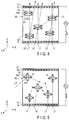
- FIG. 4 is an illustration schematically showing liquid crystal layer 30 in a transparent state.
- FIG. 5 is an illustration schematically showing the liquid crystal layer 30 in a scattering state.
- FIG. 6 is a cross-sectional view showing the display panel PNL in a case where the liquid crystal layer 30 is in a transparent state.
- FIG. 7 is a cross-sectional view showing the display panel PNL in a case where the liquid crystal layer 30 is in a scattering state.
- FIG. 8A is a cross-sectional view showing a first configuration example.
- FIG. 8B is a cross-sectional view showing a first modified example of the first configuration example.
- FIG. 8C is a cross-sectional view showing a second modified example of the first configuration example.
- FIG. 9 is a cross-sectional view for explanation of an action in a case where a functional member 100 is a light-shielding member.
- FIG. 10 is a cross-sectional view for explanation of an action in a case where the functional member 100 is a reflective member.
- FIG. 11 is a cross-sectional view showing a second configuration example.
- FIG. 12A is a cross-sectional view showing a third configuration example.
- FIG. 12B is a cross-sectional view showing a modified example of the third configuration example.
- FIG. 13 is a cross-sectional view showing a fourth configuration example.
- FIG. 14 is an illustration for explanation of diffusibility of a second functional member 120 which is a diffusing member.
- FIG. 15 is a cross-sectional view for explanation of an action of the second functional member 120 shown in FIG. 14 .
- FIG. 16 is a plan view for explanation of an action of the second functional member 120 shown in FIG. 14 .
- FIG. 17 is a plan view showing a first arrangement example.
- FIG. 18 is a plan view showing a second arrangement example.
- FIG. 19 is a plan view showing a third arrangement example.
- FIG. 20 is a plan view showing a fourth arrangement example.
- FIG. 21 is a plan view showing a fifth arrangement example.
- FIG. 22 is a plan view showing a sixth arrangement example.
- FIG. 23 is a plan view showing a seventh arrangement example.
- FIG. 24 is a plan view showing an eighth arrangement example.
- a display device comprising: a first substrate; a second substrate including a first end portion and a second end portion located at a position different from the first end portion; a polymer dispersed liquid crystal layer disposed between the first substrate and the second substrate; a light source device located above the first substrate and disposed along the first end portion; and a light-shielding member disposed on at least a part of the second end portion.
- a display device comprising: a first substrate; a second substrate including a first end portion and a second end portion located at a position different from the first end portion; a polymer dispersed liquid crystal layer disposed between the first substrate and the second substrate; a light source device located above the first substrate and disposed along the first end portion; and a reflective member disposed on at least a part of the second end portion.
- FIG. 1 is a plan view showing a configuration example of a display device DSP according to the embodiments.
- a first direction X and a second direction Y intersect each other, and a third direction Z intersects the first direction X and the second direction Y.
- the first direction X, the second direction Y, and the third direction Z are orthogonal to each other but may intersect at an angle other than ninety degrees.
- a position of a distal side of arrow indicating the third direction Z is called an upper position while a position of a back side of the arrow is called a lower position.
- the second member may be in contact with the first member or may be remote from the first member.
- an observation position at which the display device DSP is observed is assumed to be located on the distal side of the arrow indicating the third direction Z, and viewing from the observation position toward the X-Y plane defined by the first direction X and the second direction Y is called a planar view.
- the display device DSP comprises a display panel PNL and wiring substrates F 1 to F 3 .
- the display device DSP also comprises a light source device (not shown).
- the display panel PNL comprises a first substrate SUB 1 , a second substrate SUB 2 , and a third substrate SUB 3 .
- the first substrate SUB 1 , the second substrate SUB 2 , and the third substrate SUB 3 are arranged in this order in the third direction Z. and overlap in planar view.
- the display panel PNL includes a display area DA on which an image is displayed and a frame-shaped non-display area NDA surrounding the display area DA.
- the display area DA is located in an area where the first substrate SUB 1 and the second substrate SUB 2 overlap.
- the display panel PNL includes n scanning lines G (G 1 to Gn) and m signal lines S (S 1 to Sm), in the display area DA.
- n and m is a positive integer, and n may be equal to or different from m.
- the scanning lines G extend in the first direction X and are arranged at intervals in the second direction Y.
- the signal lines S extend in the second direction Y and are arranged at intervals in the first direction X.
- the first substrate SUB 1 includes end portions E 11 and E 14 extending in the first direction X, and end portions E 12 and E 13 extending in the second direction Y.
- the second substrate SUB 2 includes end portions E 21 and E 24 extending in the first direction X, and end portions E 22 and E 23 extending in the second direction Y.
- the third substrate SUB 3 includes end portions E 31 and E 34 extending in the first direction X, and end portions E 32 and E 33 extending in the second direction Y.
- the end portions E 11 , E 21 , and E 31 overlap but at least one of three end portions may be displaced, in planar view.
- the end portions E 12 , E 22 , and E 32 overlap but may be displaced from one another.
- the end portions E 13 , E 23 , and E 33 overlap but may be displaced from one another.
- the end portions 524 and E 34 are located between the end portion E 14 and the display area DA in planar view.
- the first substrate SUM 1 includes an extension portion Ex between the end portions E 14 and E 24 .
- the wiring substrates F 1 to F 3 are connected to the extension portion Ex and arranged in this order in the first direction X.
- the wiring substrate F 1 is provided with a gate driver GD 1 .
- the wiring substrate F 2 is provided with a source driver SD.
- the wiring substrate F 3 is provided with a gate driver GD 2 .
- the wiring substrates F 1 to F 3 may be replaced with a single wiring substrate.
- the signal lines S are drawn to the non-display area NDA and connected to the source driver SD.
- the scanning lines G are drawn to the non-display area NDA and connected to the gate drivers GD 1 and/or GD 2 .
- odd-numbered scanning lines G are drawn between the end portion E 13 and the display area DA and connected to the gate driver GD 2 .
- even-numbered scanning lines G are drawn between the end portion E 12 and the display area DA and connected to the gate driver GD 1 .
- the relationship in connection between the gate drivers GD 1 and GD 2 and the scanning lines G is not limited to the example illustrated.
- FIG. 2 is a perspective view showing the display device DSP shown in FIG. 1 . Illustration of the wiring substrates F 1 to F 3 is omitted.
- a light source device LU is located above the first substrate SUB 1 and disposed along the end portions E 24 and E 34 .
- the light source device LU comprises light-emitting elements LS and a wiring substrate F 4 represented by a dotted line.
- the light-emitting elements LS are arranged at intervals in the first direction X.
- Each of the light-emitting elements LS is connected to the wiring substrate F 4 .
- the light-emitting elements LS are located between the first substrate SUB 1 and the wiring substrate F 4 in the third direction Z.
- the light-emitting elements LS are, for example, light-emitting diodes.
- Each of the light-emitting elements LS comprises a light-emitting portion EM.
- the light-emitting portion EM faces the end portions E 24 and E 34 .
- the light-emitting portion EM may be in contact with the end portions E 24 and E 34 .
- an air layer, an optical element, and the like may be interposed between the light-emitting portion EM and the end portions E 24 and E 34 .
- the end portions E 24 and E 34 correspond to incidence portions in which the light emitted from the light-emitting portion EM is made incident.
- an end portion for incidence at which the light source device LU is disposed, of the end portions E 21 to E 24 of the second substrate SUB 2 corresponds to a first end portion, and the other end portion at a position different from the first end portion corresponds to a second end portion.
- An end portion located on the second end portion side, of the end portions E 11 to E 14 of the first substrate SUB 1 corresponds to a third end portion.
- An end portion located on the first end portion side, of the end portions E 31 to E 34 of the third substrate SUB 3 corresponds to the fourth end portion, and an end portion located on the second end portion side, of the end portions E 31 to E 34 , corresponds to a fifth end portion.
- the end portion E 24 corresponds to the first end portion
- the end portions E 21 to E 23 correspond to the second end portions
- the end portions E 11 to E 13 correspond to the third end portions
- the end portion E 34 corresponds to the fourth end portion
- the end portions E 31 to E 33 correspond to the fifth end portions.
- the second, third, and fifth end portions may include an end portion curved in planar view.
- the second end portions include linearly extending end portions E 21 to E 23
- the end portion E 21 opposed to the first end portion is considered as a first portion
- the end portions E 22 and E 23 which are adjacent to the first end portion and the first portion and which are opposed to each other are considered as a second portion and a third portion, respectively.
- the end portions in the present specification correspond to the side surfaces or end surfaces having widths in the third direction Z, in each of the first substrate SUB 1 , the second substrate SUB 2 , and the third substrate SUB 3 .
- FIG. 3 is a cross-sectional view showing the display device DSP shown in FIG. 1 .
- Main portions alone in the cross-section of the display device DSP in a Y-Z plane defined by the second direction Y and the third direction Z will be explained here.
- the display panel PNL comprises a liquid crystal layer 30 held between the first substrate SUB 1 and the second substrate SUB 2 .
- the first substrate SUB 1 and the second substrate SUB 2 are bonded to each other by a seal 40 .
- the third substrate SUB 3 is bonded to the second substrate SUB 2 by a transparent adhesive AD disposed across the display area DA and the non-display area NDA.
- the first substrate SUB 1 comprises a transparent substrate 10 , a pixel electrode 11 , an alignment film 12 , and the like.
- the second substrate SUB 2 comprises a transparent substrate 20 , a common electrode 21 , an alignment film 22 , and the like.
- the third substrate SUB 3 is a transparent substrate.
- the transparent substrates 10 and 20 and the third substrate SUB 3 are insulating substrates such as glass substrates or plastic substrates.
- the pixel electrodes 11 and the common electrode 21 are formed of, for example, a transparent conductive material such as indium tin oxide (ITO) or indium zinc oxide (IZO).
- the alignment films 12 and 22 may be horizontal alignment films having an alignment restriction force approximately parallel to the X-Y plane or may be vertical alignment films having an alignment restriction force approximately parallel to the third direction Z.
- the liquid crystal layer 30 is located in at least the display area DA.
- the liquid crystal layer 30 is located between the alignment films 12 and 22 .
- the transparent state and the scattering state in the liquid crystal layer 30 are controlled in response to voltages of the pixel electrodes 11 and the common electrode 21 , as explained with reference to FIG. 4 and FIG. 5 .
- the light-emitting element LS is located above the extension portion Ex. In addition, the light-emitting element LS is located between the wiring substrate F 1 to F 3 and the second substrate SUB 2 in the second direction Y.
- the light-emitting element LS emits light from the light-emitting portion EM toward the end portions E 24 and E 34 .
- the light incident on the display panel PNL from the end portions E 24 and E 34 propagates in a direction opposite to the arrow representing the second direction Y as explained below.
- the light-emitting element LS may be opposed to the end portions of the first substrate SUB 1 , the second substrate SUB 2 , and the third substrate SUB 3 , for example, the end portions E 11 , E 21 , and E 31 .
- the end portion E 11 includes the side surface of the transparent substrate 10 .
- the end portion E 21 includes a part of the side surface of the transparent substrate 20 .
- the end portion E 31 includes a part of the side surface of the third substrate SUB 3 .
- FIG. 4 is an illustration schematically showing liquid crystal layer 30 in a transparent state.
- the example illustrated in FIG. 4 corresponds to a state in which no voltage is applied to the liquid crystal layer 30 (for example, a state in which a potential difference between the pixel electrode 11 and the common electrode 21 is approximately zero).
- the liquid crystal layer 30 is a polymer dispersed liquid crystal layer including polymer 31 which is a polymeric compound and liquid crystal molecules 32 .
- the polymer 31 is liquid crystal polymer.
- the polymer 31 can be obtained by, for example, polymerizing liquid crystal monomer in a state of being aligned in a predetermined direction by the alignment restriction force of the alignment films 12 and 22 .
- the alignment treatment direction of the alignment films 12 and 22 agrees with the first direction X, and the alignment films 12 and 22 have the alignment restriction force in the first direction X.
- the polymer 31 is formed in a streaky shape or a stripe shape extending in the first direction X.
- the liquid crystal molecules 32 are dispersed in gaps of the polymer 31 and aligned such that their major axis extends in the first direction X.
- the polymer 31 and the liquid crystal molecule 32 have optical anisotropy or refractive anisotropy.
- the liquid crystal molecule 32 may be positive liquid crystal molecule having a positive dielectric anisotropy or negative liquid crystal molecule having a negative dielectric anisotropy.
- the polymer 31 and the liquid crystal molecule 32 are different in response performance to the electric field. The response performance of the polymer 31 to the electric field is lower than the response performance of the liquid crystal molecule 32 to the electric field.
- An optical axis Ax 1 of the polymer 31 and an optical axis Ax 2 of the liquid crystal molecule 32 are parallel to each other.
- each of the optical axis Ax 1 and the optical axis Ax 2 is parallel to the first direction X.
- the polymer 31 and the liquid crystal molecule 32 have approximately equivalent refractive anisotropy. In other words, ordinary refractive indexes of the polymer 31 and the liquid crystal molecule 32 are approximately equivalent to each other, and extraordinary refractive indexes of the polymer 31 and the liquid crystal molecule 32 are approximately equivalent to each other.
- the state illustrated in FIG. 4 is called a transparent state.
- the light beam L 3 corresponds to the light emitted from the light-emitting element LS shown in FIG. 3 , and propagates in a direction opposite to the direction represented by an arrow of the second direction Y while hardly scattered in the liquid crystal layer 30 .
- FIG. 5 is an illustration schematically showing the liquid crystal layer 30 in a scattering state.
- the example illustrated in FIG. 5 corresponds to a state in which a voltage is applied to the liquid crystal layer 30 (for example, a state in which a potential difference between the pixel electrode 13 and the common electrode 21 is higher than or equal to a threshold value).
- the response performance of the polymer 31 to the electric field is lower than the response performance of the liquid crystal molecule 32 to the electric field.
- the alignment direction of the polymer 31 is hardly varied irrespective of the presence or absence of the electric field.
- the alignment direction of the liquid crystal molecule 32 is varied in accordance with the electric field in a state in which a voltage higher than or equal to the threshold value is applied to the liquid crystal layer 30 .
- the optical axis Ax 1 is substantially parallel to the first direction X while the optical axis Ax 2 is oblique to the first direction X.
- the liquid crystal molecule 32 is positive liquid crystal molecule, the liquid crystal molecules 32 are aligned such that their major axes correspond to the electric field. An electric field between the pixel electrode 11 and the common electrode 21 is formed in the third direction Z. For this reason, the liquid crystal molecules 32 are aligned such that their major axes or the optical axes Ax 2 correspond to the third direction Z. In other words, the optical axes Ax 1 and optical axes Ax 2 intersect each other.
- a large refractive index difference is therefore generated between the polymer 31 and the liquid crystal molecule 32 in all directions including the first direction X, the second direction Y, and the third direction Z.
- the light beams L 1 to L 3 incident on the liquid crystal layer 30 are thereby scattered in the liquid crystal layer 30 .
- the state illustrated in FIG. 5 is called a scattering state.
- FIG. 6 is a cross-sectional view showing the display panel PNL in a case where the liquid crystal layer 30 is in a transparent state.
- a light beam L 11 emitted from the light-emitting element LS is made incident on the display panel PNL from the end portions E 24 and E 34 to propagate through the first substrate SUB 1 , the liquid crystal layer 30 , the second substrate SUB 2 , and the third substrate SUB 3 . Since the liquid crystal layer 30 is in the transparent state, the light beam L 11 is hardly scattered in the liquid crystal layer 30 , and hardly leaks from a lower surface 10 B of the transparent substrate 10 or an upper surface 3 T of the third substrate SUB 3 .
- An external light beam L 12 incident on the display panel PNL is transmitted and hardly scattered in the liquid crystal layer 30 .
- the external light beam L 12 incident on the display panel PNL from the lower surface 10 B is transmitted through the upper surface 30 T
- the external light beam L 12 incident on the display panel PNL from the upper surface 30 T is transmitted through the lower surface 10 B.
- the user can visually recognize a background on the lower surface 10 B side through the display panel PNL when observing the display panel PNL from the upper surface 30 T side.
- the user can visually recognize a background on the upper surface 3 T side through the display panel PNL when observing the display panel PNL from the lower surface 10 B side.
- FIG. 7 is a cross-sectional view showing the display panel PNL in a case where the liquid crystal layer 30 is in a scattering state.
- a light beam L 21 emitted from the light-emitting element LS is made incident on the display panel PNL from the end portions E 24 and E 34 to propagate through the display panel PNL.
- the liquid crystal layer 30 overlapping a pixel electrode 11 A is in the transparent state, the light beam L 21 is hardly scattered in an area of the liquid crystal layer 30 which overlaps the pixel electrode 11 A.
- the liquid crystal layer 30 overlapping a pixel electrode 11 B is in the scattering state. For this reason, the light beam L 21 is scattered in an area which overlaps the pixel electrode 11 B in the liquid crystal layer 30 .
- a scattered light beam L 211 which is a part of the light beam L 21 is transmitted through the upper surface 3 T, a scattered light beam L 212 which is another part of the light beam L 21 is transmitted through the lower surface 10 B, and the other scatter light beam propagates through the inside of the display panel PNL.
- an external light beam L 22 incident on the display panel PNL is transmitted and hardly scattered in the liquid crystal layer 30 , similarly to the external light beam L 12 shown in FIG. 6 .
- an external light beam L 23 incident from the lower surface 10 B is scattered in the liquid crystal layer 30 and a light beam L 231 which is a part of the external light beam L 23 is transmitted through the upper surface 3 T.
- an external light beam L 24 incident from the upper surface 3 T is scattered in the liquid crystal layer 30 and a light beam L 241 which is a part of the external light beam L 24 is transmitted through the lower surface 10 B.
- the user can visually recognize a color of the light beam L 21 in the area overlapping the pixel electrode 11 B when observing the display panel PNL from the upper surface 3 T side.
- the light beam L 231 of the external light beam L 23 is transmitted through the display panel PNL, the user can also visually recognize the background on the lower surface 10 B side through the display panel PNL.
- the user can visually recognize a color of the light beam L 21 in the area overlapping the pixel electrode 11 B when observing the display panel PNL from the lower surface 10 B side.
- the light beam L 241 of the external light beam L 24 is transmitted through the display panel PNL, the user can also visually recognize the background on the upper surface 3 T side through the display panel PNL.
- the color of the light beam L 21 can hardly be recognized visually and the user can visually recognize the background through the display panel PNL since the liquid crystal layer 30 is in the transparent state.
- the light beam L 11 shown in FIG. 6 often leaks to the outside after reaching the end portion E 31 .
- the light having propagated through the display panel PNL may also leak on the end portions E 11 and E 21 .
- the occurrence of undesired light leakage may cause an impression of the appearance of the display device DSP to be degraded.
- the proximity to the end portion E 21 is located remote from the light source device LU and tends to have a lower luminance as compared with the proximity to the end portion E 24 , which is the incidence portion. This difference in luminance between the proximity to the end portion E 21 and the proximity to the end portion E 24 may cause the display quality to be degraded.
- first to fourth configuration examples will be hereinafter disclosed in the present specification to suppress undesired light leakage.
- FIG. 8A is a cross-sectional view showing a first configuration example.
- the display device DSP comprises a functional member 100 having an optical function.
- the functional member 100 is, for example, a light-shielding member, a reflective member, a diffusing member, or the like.
- the functional member 100 is disposed on the end portion E 21 . In the example illustrated in FIG. 8A , the functional member 100 is in contact with the end portion E 21 .
- the functional member 100 may be a thin film formed directly on the end portion E 21 or a thin film bonded to the end portion E 21 by an adhesive.
- the functional member 100 is also disposed on the end portions E 11 and E 31 .
- the functional member 100 is also in contact with the end portions E 11 and E 31 .
- the functional member 100 may be disposed on the end portions E 11 , E 21 , and E 31 separately or integrally.
- the end portions E 11 , E 21 , and E 31 are located on the same plane parallel to X-Z plane defined by the first direction X and the third direction Z.
- the end portion E 21 is located just above the end portion E 11
- the end portion E 31 is located just above the end portion E 21 .
- the single functional member 100 is disposed on the end portions E 11 , E 21 , and E 31 .
- FIG. 8B is a cross-sectional view showing a first modified example of the first configuration example.
- the third substrate SUB 3 is disposed below the first substrate SUB 1 and bonded to the first substrate SUB 1 .
- the functional member 100 is disposed on the end portions E 11 , E 21 , and E 31 .
- FIG. 8C is a cross-sectional view showing a second modified example of the first configuration example.
- the second modified example is different from the first modified example with respect to a feature that the end portions E 34 , E 14 , and E 24 are arranged in the third direction Z in this order and the end portions are located on the same plane substantially parallel to X-Z plane.
- the end portions E 34 , E 14 , and E 24 are opposed to the light-emitting element LS in the second direction Y.
- FIG. 9 is a cross-sectional view for explanation of an action in a case where a functional member 100 is a light-shielding member.
- the light-shielding member is formed of, for example, a resin material colored in block or a light-shielding metal material.
- a light beam L 31 emitted from the light-emitting element LS is made incident from the end portions E 24 and E 34 to propagate through the first substrate SUB 1 , the second substrate SUB 2 , and the third substrate SUB 3 .
- the light beam L 31 having reached the end portion E 21 is blocked by the functional member 100 .
- the light beam L 31 having reached the end portions E 11 and E 31 is also blocked by the functional member 100 . For this reason, undesired light leakage can be suppressed. Degradation in impression of the appearance can be therefore suppressed in the display device DSP.
- FIG. 10 is a cross-sectional view for explanation of an action in a case where the functional member 100 is a reflective member.
- the reflective member is formed of, for example, a metal material having a high reflectance such as aluminum, silver, or titanium.
- a light beam L 31 emitted from the light-emitting element LS is made incident from the end portions E 24 and E 34 to propagate through the first substrate SUB 1 , the second substrate SUB 2 , and the third substrate SUB 3 .
- the light beam L 31 having reached the end portion E 21 is reflected to the light-emitting element LS side by the functional member 100 .
- the light beam L 31 having reached the end portions E 11 and E 31 is also reflected by the functional member 100 .
- the end portion E 24 corresponds to the first portion
- the end portion E 21 corresponds to the second end portion
- the end portion E 11 corresponds to the third end portion
- the end portion E 34 corresponds to the fourth end portion
- the end portion E 31 corresponds to the fifth end portion.
- FIG. 11 is a cross-sectional view showing a second configuration example.
- the second configuration example is different from the first configuration example with respect to a feature that the functional member 100 is also disposed on the lower surface 10 B and the upper surface 3 T of the non-display area NDA.
- the single functional member 100 is disposed on the end portions E 11 , E 21 , and E 31 , a portion exceeding the end portion E 11 is bent and disposed on the lower surface 10 B, and a portion exceeding the end portion E 31 is bent and disposed on the upper surface 3 T.
- the functional member 100 is in contact with each of the end portions E 11 , E 21 , and E 31 , the lower surface 10 B, and the upper surface 3 T.
- the functional member 100 may be a light-shielding member or a reflective member as explained above.
- FIG. 12A is a cross-sectional view showing a third configuration example.
- the third configuration example is different from the first configuration example with respect to a feature of comprising a plurality of functional members 100 A and 100 B.
- the end portion E 21 is located just above the end portion E 11
- the end portions E 31 is not located just above the end portion E 21 but displaced from the end portion E 21 in the second direction Y.
- the functional member 100 A is disposed on the end portions E 11 and E 21
- the functional member 100 B is disposed on the end portion E 31 .
- the functional members 100 A and 100 B may be light-shielding members or reflective members as explained above.
- the functional members may be separated in accordance with the number of the end portions arranged in the third direction Z or the functional members may be disposed on the end portions E 11 , E 21 , and E 31 , respectively.
- the same advantages as those of the first configuration example can be obtained.
- the functional members 100 A and 100 B are hardly peeled off from the end portions E 11 , E 21 , and E 31 .
- the functional members 100 A and 100 B are reflective members, degradation in display quality which results from non-uniformity in reflected light can be suppressed.
- FIG. 12B is a cross-sectional view showing a modified example.
- the single functional member 100 is disposed on the end portions E 11 , E 21 , and E 31 , bent between the end portions E 21 and E 31 , and disposed on an upper surface 2 T of the second substrate SUB 2 .
- the functional member 100 is in contact with the upper surface 2 T at a position between the end portions E 21 and E 31 .
- the functional member 100 may be a light-shielding member or a reflective member as explained above.
- FIG. 13 is a cross-sectional view showing a fourth configuration example.
- the fourth configuration example is different from the first configuration example with respect to a feature of comprising a first functional member 110 and a second functional member 120 having a function different from the first functional member 110 .
- the second functional member 120 is in contact with the end portion E 21
- the first functional member 110 is in contact with the second functional member 120 .
- the other functional members may be disposed between the first functional member 110 and the end portion E 21 .
- the first functional member 110 may be a thin film formed directly on the end portion E 21 and the second functional member 120 may be a thin film formed directly on the first functional member 110 , or the first functional member 110 may be a thin film and the second functional member 120 may be an adhesive to bond the first functional member 110 to the end portion E 21 .
- the first functional member 110 is a reflective member
- the second functional member 120 is a diffusing member.
- the stacked layer body of the first functional member 110 and the second functional member 120 is also disposed on the end portions E 11 and E 31 .
- the second functional member 120 is in contact with each of the end portions E 11 and E 31 .
- the single first functional member 110 and the single second functional member 120 overlap in the second direction Y, and the first functional member 110 and the second functional member 120 are disposed on the end portions E 11 , E 21 , and E 31 .
- the first functional member 110 and the second functional member 120 may extend to the lower surface 10 B and the upper surface 3 T, similarly to the second configuration example.
- the first functional member 110 and the second functional member 120 may be separated to be disposed on the respective end portions, similarly to the third configuration example.
- FIG. 14 is an illustration for explanation of diffusibility of a second functional member 120 which is a diffusing member.
- the second functional member 120 diffuses the light incident in the second direction Y into the X-Z plane.
- the second functional member 120 explained here is an anisotropically diffusing member having diffusibility Dx in the first direction X larger than diffusibility Dz in the third direction Z.
- the longitudinal direction of the end portion E 21 is parallel to the first direction X
- the thickness direction of the end portion E 21 is parallel to the third direction Z.
- the light passing through the second functional member 120 is diffused more largely in the longitudinal direction of the end portion E 21 than in the thickness direction of the end portion E 21 .
- FIG. 15 is a cross-sectional view for explanation of an action of the second functional member 120 shown in FIG. 14 . Since the second functional member 120 has smaller diffusibility Dz, the diffusion in the third direction Z, of the light reflected by the first functional member 110 can be suppressed. For this reason, leakage of the reflected light from the lower surface 10 B and the upper surface 3 T can be suppressed.
- FIG. 16 is a plan view for explanation of an action of the second functional member 120 shown in FIG. 14 . Since the second functional member 120 has larger diffusibility Dx, the light reflected by the first functional member 110 is diffused in the first direction X and the luminance of the reflected light can be uniformed at positions close to the end portion E 21 and the like. In addition, even if the end portion E 21 and the like have cracks or fine unevenness, the luminance of the reflected light can be uniformed by the diffusing effect of the second functional member 120 .
- FIG. 17 is a plan view showing a first arrangement example.
- the single functional member 100 is disposed on the only end portions E 11 , E 21 , and E 31 on the side opposite to the end portions E 24 and E 34 , which are the incidence portions.
- the functional member 100 is a light-shielding member or a reflective member. If the functional member 100 is a light-shielding member, the light leakage at the end portion E 21 can be suppressed. If the functional member 100 is a reflective member, the light leakage at the end portion E 21 can be suppressed and the degradation in luminance on the end portion E 21 side can also be suppressed.
- FIG. 18 is a plan view showing a second arrangement example.
- the second arrangement example is different from the fifth arrangement example with respect to a feature of comprising functional members 101 to 103 .
- the functional member 101 is disposed on the end portions E 11 , E 21 , and E 31 extending in the first direction X.
- the functional member 102 is disposed on the end portions E 12 , E 22 , and E 32 extending in the second direction Y.
- the functional member 103 is disposed on end portions E 13 , E 23 , and E 33 extending in the second direction Y.
- Each of the functional members 101 to 103 is formed independently.
- the functional members 101 to 103 are light-shielding members or reflective members.
- All of the functional members 101 to 103 may be light-shielding members or reflective members.
- a combination of the functional member 101 which is a reflective member and the functional members 102 and 103 which are light-shielding members, a combination of the functional member 101 which is a light-shielding member and the functional members 102 and 103 which are reflective members, and the like can be applied.
- the functional members 102 and 103 are light-shielding members, the functional members 102 and 103 can also suppress the light leakage at the end portions E 22 and E 23 . If the functional members 102 and 103 are reflective members, the functional members 102 and 103 can suppress the light leakage at the end portions E 22 and E 23 and the degradation in luminance on the end portion E 22 side and the end portion E 23 side.
- FIG. 19 is a plan view showing a third arrangement example.
- the third arrangement example is different from the first arrangement example with respect to a feature that the single functional member 100 is disposed along three sides except the incidence portions.
- the functional member 100 is disposed on the end portions E 11 , E 21 , and E 31 , disposed on the end portions E 12 , E 22 , and E 32 , and disposed on the end portions E 13 , E 23 , and E 33 .
- the functional member 100 is a light-shielding member or a reflective member.
- FIG. 20 is a plan view showing a fourth arrangement example.
- the fourth arrangement example is different from the first arrangement example with respect to a feature of comprising a first functional member 111 and a second functional member 121 different in function.
- the second functional member 121 is in contact with the end portions E 11 , E 21 , and E 31 .
- the first functional member 111 overlaps the second functional member 121 .
- the first functional member 111 is a reflective member
- the second functional member 121 is a diffusing member.
- the light leakage at the end portion E 21 can be suppressed, the degradation in luminance on the end portion E 21 side can be suppressed, and the luminance can be uniformed.
- FIG. 21 is a plan view showing a fifth arrangement example.
- the fifth arrangement example is different from the fourth arrangement example with respect to a feature of comprising first functional members 112 and 113 besides the first functional member 111 .
- the first functional member 112 is in contact with the end portions E 12 , E 22 , and E 32 .
- the first functional member 113 is in contact with the end portions E 13 , E 23 , and E 33 .
- the first functional members 111 to 113 are reflective members
- the second functional member 121 is a diffusing member.
- FIG. 22 is a plan view showing a sixth arrangement example.
- the sixth arrangement example is different from the fifth arrangement example with respect to a feature of further comprising second functional members 122 and 123 .
- the second functional member 122 is in contact with the end portions E 12 , E 22 , and E 32 .
- the first functional member 112 overlaps the second functional member 122 .
- the second functional member 123 is in contact with the end portions E 13 , E 23 , and E 33 .
- the first functional member 113 overlaps the second functional member 123 .
- the first functional members 111 to 113 are reflective members
- the second functional members 121 to 123 are diffusing members.
- the same advantages as those of the fourth arrangement example can be obtained.
- degradation in the luminance on the end portion E 22 side and the end portion E 23 side can be suppressed, and the luminance can be uniformed.
- FIG. 23 is a plan view showing a seventh arrangement example.
- the seventh arrangement example is different from the above-explained arrangement examples with respect to a feature of comprising light source devices LU 1 and LU 2 .
- the first substrate SUB 1 comprises extension portions Ex 1 and Ex 2 further extending in the second direction Y than the second substrate SUB 2 and the third substrate SUBS.
- the light source device LU 1 is located above the extension portion Ex 1
- the light source device LU 2 is located above the extension portion Ex 2 .
- the light source device LU 1 is disposed along the end portions E 24 and E 34 .
- the light source device LU 1 comprises light-emitting elements LS 1 arranged at intervals in the first direction X, and a wiring substrate F 4 to which the light-emitting elements LS 1 are connected.
- two light-emitting elements LS 1 arranged in the first direction X correspond to a first light-emitting element and a second light-emitting element, respectively.
- a second functional member 124 located between two light-E 24 and E 34 , and the first functional member 114 overlaps the second functional member 124 .
- the light source device LU 2 is disposed along the end portions E 21 and E 31 .
- the light source device LU 2 comprises light-emitting elements LS 2 arranged at intervals in the first direction X, and a wiring substrate F 5 to which the light-emitting elements LS 2 are connected.
- a second functional member 121 located between two light-emitting elements LS 2 is disposed on the end portions E 21 and E 31 , and the first functional member 111 overlaps the second functional member 121 .
- the first functional members 111 and 114 are reflective members, and the second functional members 121 and 124 are diffusing members.
- the light emitted from the light-emitting elements LS 1 is made incident from the end portions E 24 and E 34 to propagate toward the end portions E 21 and E 31 .
- the light having reached the end portions E 21 and E 31 is diffused by the second functional member 121 and reflected by the first functional member 111 .
- the light emitted from the light-emitting elements LS 2 is made incident from the end portions E 21 and E 31 to propagate toward the end portions E 24 and E 34 .
- the light having reached the end portions E 24 and E 34 is diffused by the second functional member 124 and reflected by the first functional member 114 .
- FIG. 24 is a plan view showing an eighth arrangement example.
- the eighth arrangement example is different from the above-explained arrangement examples with respect to a feature that the first substrate SUB 1 , the second substrate SUB 2 , and the third substrate SUB 3 have different shapes.
- the first substrate SUB 1 includes an end portion E 15 extending in the first direction X, and an end portion 516 having at least a part formed in a curved shape in planar view.
- the first substrate SUB 1 is formed in an ellipsoidal shape (or a track shape) in planar view.
- the first substrate SUB 1 , the second substrate SUB 2 and the third substrate SUB 3 are formed in substantially the same shape.
- the second substrate SUB 2 includes an end portion E 25 located on the end portion 515 side and an end portion E 26 located on the end portion E 16 side.
- the third substrate SUB 3 includes an end portion E 35 located on the end portion E 15 side and an end portion E 36 located on the end portion 516 side.
- the light source device LU is disposed along the end portions E 15 , E 25 , and E 35 .
- the second functional member 120 is disposed on the end portions E 16 , E 26 , and E 36 .
- the first functional member 110 overlaps the second functional member 120 .
- a display device capable of suppressing the undesired light leakage can be provided by the present embodiments.
- the present invention is not limited to the embodiments described above but the constituent elements of the invention can be modified in various manners without departing from the spirit and scope of the invention.
- Various aspects of the invention can also be extracted from any appropriate combination of a plurality of constituent elements disclosed in the embodiments. For example, some structural elements may be deleted from the entire structural elements in the embodiments. Furthermore, structural elements described in different embodiments may be combined suitably.
- the configuration examples employing the polymer dispersed liquid crystal for the display panel PNL have been explained, but the configuration examples may be employed in an illumination device combined with a transmissive display panel or a reflective display panel. According to the illumination device, the scattering state and the transparent state can be changed on not only the entire surface of the display area DA, but also a partial surface of the display area DA. In addition, loss resulting from undesired scattering and undesired absorption can be reduced and the efficiency of use of the light can be improved, by employing the above-explained configuration examples.
- a display device comprising:
- a second substrate including a first end portion and a second end portion located at a position different from the first end portion
- a polymer dispersed liquid crystal layer disposed between the first substrate and the second substrate;
- a light source device located above the first substrate and disposed along the first end portion;
- a light-shielding member disposed on at least a part of the second end portion.
- the first substrate includes a third end portion located on the second end portion side, and
- the light-shielding member is disposed on at least a part of the third end portion.
- the display device according to (1) or (2), further comprising:
- the second substrate is located between the first substrate and the third substrate
- the third substrate includes a fourth end portion located on the first end portion side and a fifth end portion located on the second end portion side,
- the light source device is disposed along the fourth end portion, and
- the light-shielding member is disposed on at least a part of the fifth end portion.
- a display device comprising:
- a second substrate including a first end portion and a second end portion located at a position different from the first end portion
- a polymer dispersed liquid crystal layer disposed between the first substrate and the second substrate;
- a light source device located above the first substrate and disposed along the first end portion;
- a reflective member disposed on at least a part of the second end portion.
- the display device further comprising:
- a diffusing member located between the second end portion and the reflective member.
- the diffusing member is an anisotropically diffusing member.
- the first substrate includes a third end portion located on the second end portion side, and
- the reflective member is disposed on at least a part of the third end portion.
- the display device according to any one of (4) to (7), further comprising:
- the second substrate is located between the first substrate and the third substrate
- the third substrate includes a fourth end portion located on the first end portion side and a fifth end portion located on the second end portion side,
- the second end portion includes a first portion opposed to the first end portion, and a second portion and a third portion which are opposed to each other,
- the second portion and the third portion are adjacent to the first end portion and the first portion, respectively,
- the reflective member and the diffusing member are disposed on the first portion
- the diffusing member is in contact with the first portion.
- the reflective member and the diffusing member are disposed on the second portion and the third portion, and
- the diffusing member is in contact with each of the second portion and the third portion.
- the reflective member is disposed on the second portion and the third portion, and
- the reflective member is in contact with each of the second portion and the third portion.
- the light source device comprises:
- the diffusing member is located between the first light-emitting element and the second light-emitting element, at the first end portion.
- the polymer dispersed liquid crystal layer includes a polymer formed of a polymeric material and liquid crystal molecules dispersed in the polymer.
- the first substrate comprises a pixel electrode
- the second substrate comprises a common electrode
- a transparent state and a scattering state of the polymer dispersed liquid crystal layer are controlled in accordance with voltages applied to the pixel electrode and the common electrode.
Landscapes
- Physics & Mathematics (AREA)
- Nonlinear Science (AREA)
- Chemical & Material Sciences (AREA)
- Mathematical Physics (AREA)
- Crystallography & Structural Chemistry (AREA)
- General Physics & Mathematics (AREA)
- Optics & Photonics (AREA)
- Dispersion Chemistry (AREA)
- Liquid Crystal (AREA)
- Planar Illumination Modules (AREA)
Abstract
Description
Claims (12)
Priority Applications (5)
| Application Number | Priority Date | Filing Date | Title |
|---|---|---|---|
| US16/903,784 US11187932B2 (en) | 2017-09-14 | 2020-06-17 | Display device |
| US17/495,236 US11624948B2 (en) | 2017-09-14 | 2021-10-06 | Display device |
| US18/180,275 US11892722B2 (en) | 2017-09-14 | 2023-03-08 | Display device |
| US18/544,667 US12153302B2 (en) | 2017-09-14 | 2023-12-19 | Display device |
| US18/916,832 US20250035974A1 (en) | 2017-09-14 | 2024-10-16 | Display device |
Applications Claiming Priority (2)
| Application Number | Priority Date | Filing Date | Title |
|---|---|---|---|
| JP2017177073A JP7005243B2 (en) | 2017-09-14 | 2017-09-14 | Display device |
| JP2017-177073 | 2017-09-14 |
Related Child Applications (1)
| Application Number | Title | Priority Date | Filing Date |
|---|---|---|---|
| US16/903,784 Continuation US11187932B2 (en) | 2017-09-14 | 2020-06-17 | Display device |
Publications (2)
| Publication Number | Publication Date |
|---|---|
| US20190079324A1 US20190079324A1 (en) | 2019-03-14 |
| US10725327B2 true US10725327B2 (en) | 2020-07-28 |
Family
ID=65631085
Family Applications (6)
| Application Number | Title | Priority Date | Filing Date |
|---|---|---|---|
| US16/130,256 Active US10725327B2 (en) | 2017-09-14 | 2018-09-13 | Display device |
| US16/903,784 Active US11187932B2 (en) | 2017-09-14 | 2020-06-17 | Display device |
| US17/495,236 Active US11624948B2 (en) | 2017-09-14 | 2021-10-06 | Display device |
| US18/180,275 Active US11892722B2 (en) | 2017-09-14 | 2023-03-08 | Display device |
| US18/544,667 Active US12153302B2 (en) | 2017-09-14 | 2023-12-19 | Display device |
| US18/916,832 Pending US20250035974A1 (en) | 2017-09-14 | 2024-10-16 | Display device |
Family Applications After (5)
| Application Number | Title | Priority Date | Filing Date |
|---|---|---|---|
| US16/903,784 Active US11187932B2 (en) | 2017-09-14 | 2020-06-17 | Display device |
| US17/495,236 Active US11624948B2 (en) | 2017-09-14 | 2021-10-06 | Display device |
| US18/180,275 Active US11892722B2 (en) | 2017-09-14 | 2023-03-08 | Display device |
| US18/544,667 Active US12153302B2 (en) | 2017-09-14 | 2023-12-19 | Display device |
| US18/916,832 Pending US20250035974A1 (en) | 2017-09-14 | 2024-10-16 | Display device |
Country Status (2)
| Country | Link |
|---|---|
| US (6) | US10725327B2 (en) |
| JP (1) | JP7005243B2 (en) |
Cited By (2)
| Publication number | Priority date | Publication date | Assignee | Title |
|---|---|---|---|---|
| US11187932B2 (en) * | 2017-09-14 | 2021-11-30 | Japan Display Inc. | Display device |
| US20230314865A1 (en) * | 2018-10-09 | 2023-10-05 | Japan Display Inc. | Display device and illumination device |
Families Citing this family (11)
| Publication number | Priority date | Publication date | Assignee | Title |
|---|---|---|---|---|
| JP2020160322A (en) * | 2019-03-27 | 2020-10-01 | 株式会社ジャパンディスプレイ | Display device |
| JP2020177731A (en) * | 2019-04-15 | 2020-10-29 | 株式会社ジャパンディスプレイ | Cover glass and display device |
| JP2020181050A (en) * | 2019-04-24 | 2020-11-05 | 株式会社ジャパンディスプレイ | Display device |
| JP7368978B2 (en) * | 2019-07-31 | 2023-10-25 | 株式会社ジャパンディスプレイ | Display device with sensor |
| JP2021032938A (en) | 2019-08-19 | 2021-03-01 | 株式会社ジャパンディスプレイ | Display |
| JP2021156944A (en) * | 2020-03-25 | 2021-10-07 | 株式会社ジャパンディスプレイ | Display device |
| CN116745693A (en) * | 2021-01-14 | 2023-09-12 | 株式会社日本显示器 | display device |
| CN112859409A (en) * | 2021-02-09 | 2021-05-28 | 捷开通讯(深圳)有限公司 | Display panel, display panel assembly and electronic equipment |
| JP7652607B2 (en) * | 2021-03-30 | 2025-03-27 | 株式会社ジャパンディスプレイ | Alignment film material and liquid crystal display device |
| JP7811277B2 (en) * | 2022-10-14 | 2026-02-04 | アルプスアルパイン株式会社 | display device |
| JP2024171122A (en) * | 2023-05-29 | 2024-12-11 | 株式会社ジャパンディスプレイ | Display device |
Citations (15)
| Publication number | Priority date | Publication date | Assignee | Title |
|---|---|---|---|---|
| US6229585B1 (en) * | 1997-10-21 | 2001-05-08 | Rohm Co., Ltd. | Liquid crystal display unit having light on one substrate illuminating edge of other |
| US6474824B1 (en) * | 1998-12-28 | 2002-11-05 | Seiko Epson Corporation | Surface-emitting device, front light, and liquid crystal device |
| US20100085510A1 (en) | 2008-10-07 | 2010-04-08 | Sony Corporation | Illuminating device, display device, and method of manufacturing light modulation element |
| US20110109663A1 (en) | 2009-11-06 | 2011-05-12 | Sony Corporation | Illuminating device and display unit |
| US20120098875A1 (en) | 2010-10-20 | 2012-04-26 | Sony Corporation | Illumination device and display device |
| US20120281273A1 (en) * | 2011-05-02 | 2012-11-08 | Sony Corporation | Display and illumination unit |
| US20130257880A1 (en) | 2012-03-27 | 2013-10-03 | Qualcomm Mems Technologies, Inc. | Light guide with internal light recirculation |
| US20140055835A1 (en) | 2011-05-09 | 2014-02-27 | Sony Corporation | Illumination device and display unit |
| US20140240642A1 (en) | 2011-10-05 | 2014-08-28 | Sony Corporation | Illumination unit, display, and electronic apparatus |
| US20150293402A1 (en) | 2012-08-08 | 2015-10-15 | Sony Corporation | Display apparatus and illumination unit |
| US20160070047A1 (en) | 2014-09-05 | 2016-03-10 | Japan Display Inc. | Display device and light source device |
| US20170160592A1 (en) | 2015-12-07 | 2017-06-08 | Japan Display Inc. | Display device |
| US20170269433A1 (en) | 2016-03-15 | 2017-09-21 | Japan Display Inc. | Display device |
| US20170285420A1 (en) | 2016-04-01 | 2017-10-05 | Japan Display Inc. | Display device |
| US20180031758A1 (en) | 2016-08-01 | 2018-02-01 | Japan Display Inc. | Display apparatus |
Family Cites Families (12)
| Publication number | Priority date | Publication date | Assignee | Title |
|---|---|---|---|---|
| JPH10123514A (en) * | 1996-10-21 | 1998-05-15 | Hitachi Ltd | Liquid crystal display |
| JPH11119206A (en) * | 1997-10-08 | 1999-04-30 | Seiko Instruments Inc | Reflection type color liquid crystal display device and its production |
| JPH11259007A (en) * | 1998-03-10 | 1999-09-24 | Sony Corp | Reflective display |
| US20100008551A9 (en) | 1998-08-18 | 2010-01-14 | Ilya Schiller | Using handwritten information |
| JP2002268061A (en) | 2001-03-09 | 2002-09-18 | Nitto Denko Corp | Reflective liquid crystal display |
| US20060014085A1 (en) * | 2002-11-14 | 2006-01-19 | Tomoegawa Paper Co., Ltd. | Anisotropic light diffusion adhesive layer, anisotropic light diffusion adhesive laminate, and illuminating device having anisotropic light diffusion adhesive laminate |
| JP2006259115A (en) * | 2005-03-16 | 2006-09-28 | Omron Corp | Double-sided display device and surface light source device |
| JP2011039305A (en) | 2009-08-11 | 2011-02-24 | Sony Ericsson Mobile Communications Ab | Display apparatus and mobile terminal |
| US11016336B2 (en) | 2016-02-12 | 2021-05-25 | Microsoft Technology Licensing, Llc | Bragg grating-based display filtering |
| JP2017156718A (en) | 2016-03-04 | 2017-09-07 | 株式会社ジャパンディスプレイ | Display device |
| JP2017195163A (en) * | 2016-04-22 | 2017-10-26 | 川崎重工業株式会社 | Light guide plate and surface lighting device |
| JP7005243B2 (en) * | 2017-09-14 | 2022-01-21 | 株式会社ジャパンディスプレイ | Display device |
-
2017
- 2017-09-14 JP JP2017177073A patent/JP7005243B2/en active Active
-
2018
- 2018-09-13 US US16/130,256 patent/US10725327B2/en active Active
-
2020
- 2020-06-17 US US16/903,784 patent/US11187932B2/en active Active
-
2021
- 2021-10-06 US US17/495,236 patent/US11624948B2/en active Active
-
2023
- 2023-03-08 US US18/180,275 patent/US11892722B2/en active Active
- 2023-12-19 US US18/544,667 patent/US12153302B2/en active Active
-
2024
- 2024-10-16 US US18/916,832 patent/US20250035974A1/en active Pending
Patent Citations (18)
| Publication number | Priority date | Publication date | Assignee | Title |
|---|---|---|---|---|
| US6229585B1 (en) * | 1997-10-21 | 2001-05-08 | Rohm Co., Ltd. | Liquid crystal display unit having light on one substrate illuminating edge of other |
| US6474824B1 (en) * | 1998-12-28 | 2002-11-05 | Seiko Epson Corporation | Surface-emitting device, front light, and liquid crystal device |
| US20100085510A1 (en) | 2008-10-07 | 2010-04-08 | Sony Corporation | Illuminating device, display device, and method of manufacturing light modulation element |
| JP2010092682A (en) | 2008-10-07 | 2010-04-22 | Sony Corp | Illuminating device, display device, and manufacturing method of light modulation element |
| US20110109663A1 (en) | 2009-11-06 | 2011-05-12 | Sony Corporation | Illuminating device and display unit |
| JP5467389B2 (en) | 2009-11-06 | 2014-04-09 | ソニー株式会社 | Illumination device and display device |
| US20120098875A1 (en) | 2010-10-20 | 2012-04-26 | Sony Corporation | Illumination device and display device |
| US20120281273A1 (en) * | 2011-05-02 | 2012-11-08 | Sony Corporation | Display and illumination unit |
| US20140055835A1 (en) | 2011-05-09 | 2014-02-27 | Sony Corporation | Illumination device and display unit |
| US20140240642A1 (en) | 2011-10-05 | 2014-08-28 | Sony Corporation | Illumination unit, display, and electronic apparatus |
| US20130257880A1 (en) | 2012-03-27 | 2013-10-03 | Qualcomm Mems Technologies, Inc. | Light guide with internal light recirculation |
| US20150293402A1 (en) | 2012-08-08 | 2015-10-15 | Sony Corporation | Display apparatus and illumination unit |
| US20160070047A1 (en) | 2014-09-05 | 2016-03-10 | Japan Display Inc. | Display device and light source device |
| JP2016057338A (en) | 2014-09-05 | 2016-04-21 | 株式会社ジャパンディスプレイ | Display device and light source device |
| US20170160592A1 (en) | 2015-12-07 | 2017-06-08 | Japan Display Inc. | Display device |
| US20170269433A1 (en) | 2016-03-15 | 2017-09-21 | Japan Display Inc. | Display device |
| US20170285420A1 (en) | 2016-04-01 | 2017-10-05 | Japan Display Inc. | Display device |
| US20180031758A1 (en) | 2016-08-01 | 2018-02-01 | Japan Display Inc. | Display apparatus |
Cited By (6)
| Publication number | Priority date | Publication date | Assignee | Title |
|---|---|---|---|---|
| US11187932B2 (en) * | 2017-09-14 | 2021-11-30 | Japan Display Inc. | Display device |
| US11624948B2 (en) | 2017-09-14 | 2023-04-11 | Japan Display Inc. | Display device |
| US11892722B2 (en) | 2017-09-14 | 2024-02-06 | Japan Display Inc. | Display device |
| US12153302B2 (en) | 2017-09-14 | 2024-11-26 | Japan Display Inc. | Display device |
| US20230314865A1 (en) * | 2018-10-09 | 2023-10-05 | Japan Display Inc. | Display device and illumination device |
| US11988917B2 (en) * | 2018-10-09 | 2024-05-21 | Japan Display Inc. | Display device and illumination device |
Also Published As
| Publication number | Publication date |
|---|---|
| US20230221593A1 (en) | 2023-07-13 |
| US20240118568A1 (en) | 2024-04-11 |
| US12153302B2 (en) | 2024-11-26 |
| JP7005243B2 (en) | 2022-01-21 |
| US11624948B2 (en) | 2023-04-11 |
| US20200310173A1 (en) | 2020-10-01 |
| US20250035974A1 (en) | 2025-01-30 |
| JP2019053186A (en) | 2019-04-04 |
| US11892722B2 (en) | 2024-02-06 |
| US11187932B2 (en) | 2021-11-30 |
| US20220026750A1 (en) | 2022-01-27 |
| US20190079324A1 (en) | 2019-03-14 |
Similar Documents
| Publication | Publication Date | Title |
|---|---|---|
| US11892722B2 (en) | Display device | |
| US11940687B2 (en) | Display device | |
| US11886066B2 (en) | Display device | |
| US11668867B2 (en) | Display device | |
| US20200326581A1 (en) | Cover glass and display device | |
| US12386229B2 (en) | Display device | |
| JP2011209690A (en) | Liquid crystal display device | |
| US10634953B2 (en) | Display device | |
| JP5459728B2 (en) | Liquid crystal display | |
| CN111679519B (en) | display device | |
| US20240329294A1 (en) | Illumination device and display device | |
| US20230280518A1 (en) | Display device | |
| JP2026015947A (en) | display device | |
| JP2026022946A (en) | Display device and lighting device |
Legal Events
| Date | Code | Title | Description |
|---|---|---|---|
| AS | Assignment |
Owner name: JAPAN DISPLAY INC., JAPAN Free format text: ASSIGNMENT OF ASSIGNORS INTEREST;ASSIGNORS:NUMATA, YUDAI;OKUYAMA, KENTARO;SIGNING DATES FROM 20180525 TO 20180528;REEL/FRAME:046867/0755 |
|
| FEPP | Fee payment procedure |
Free format text: ENTITY STATUS SET TO UNDISCOUNTED (ORIGINAL EVENT CODE: BIG.); ENTITY STATUS OF PATENT OWNER: LARGE ENTITY |
|
| STPP | Information on status: patent application and granting procedure in general |
Free format text: DOCKETED NEW CASE - READY FOR EXAMINATION |
|
| STPP | Information on status: patent application and granting procedure in general |
Free format text: NON FINAL ACTION MAILED |
|
| STPP | Information on status: patent application and granting procedure in general |
Free format text: RESPONSE TO NON-FINAL OFFICE ACTION ENTERED AND FORWARDED TO EXAMINER |
|
| STPP | Information on status: patent application and granting procedure in general |
Free format text: NON FINAL ACTION MAILED |
|
| STPP | Information on status: patent application and granting procedure in general |
Free format text: NOTICE OF ALLOWANCE MAILED -- APPLICATION RECEIVED IN OFFICE OF PUBLICATIONS |
|
| STPP | Information on status: patent application and granting procedure in general |
Free format text: PUBLICATIONS -- ISSUE FEE PAYMENT VERIFIED |
|
| STCF | Information on status: patent grant |
Free format text: PATENTED CASE |
|
| MAFP | Maintenance fee payment |
Free format text: PAYMENT OF MAINTENANCE FEE, 4TH YEAR, LARGE ENTITY (ORIGINAL EVENT CODE: M1551); ENTITY STATUS OF PATENT OWNER: LARGE ENTITY Year of fee payment: 4 |
|
| AS | Assignment |
Owner name: MAGNOLIA WHITE CORPORATION, JAPAN Free format text: ASSIGNMENT OF ASSIGNORS INTEREST;ASSIGNOR:JAPAN DISPLAY INC.;REEL/FRAME:072130/0313 Effective date: 20250625 Owner name: MAGNOLIA WHITE CORPORATION, JAPAN Free format text: ASSIGNMENT OF ASSIGNOR'S INTEREST;ASSIGNOR:JAPAN DISPLAY INC.;REEL/FRAME:072130/0313 Effective date: 20250625 |