US10714524B2 - Circuit board, semiconductor device, imaging device, solid-state image sensor, method for manufacturing solid-state image sensor, and electronic apparatus - Google Patents
Circuit board, semiconductor device, imaging device, solid-state image sensor, method for manufacturing solid-state image sensor, and electronic apparatus Download PDFInfo
- Publication number
- US10714524B2 US10714524B2 US16/086,904 US201716086904A US10714524B2 US 10714524 B2 US10714524 B2 US 10714524B2 US 201716086904 A US201716086904 A US 201716086904A US 10714524 B2 US10714524 B2 US 10714524B2
- Authority
- US
- United States
- Prior art keywords
- cavities
- image sensor
- solid
- state image
- cavity
- Prior art date
- Legal status (The legal status is an assumption and is not a legal conclusion. Google has not performed a legal analysis and makes no representation as to the accuracy of the status listed.)
- Expired - Fee Related
Links
Images


Classifications
-
- H01L27/14632—
-
- H—ELECTRICITY
- H10—SEMICONDUCTOR DEVICES; ELECTRIC SOLID-STATE DEVICES NOT OTHERWISE PROVIDED FOR
- H10F—INORGANIC SEMICONDUCTOR DEVICES SENSITIVE TO INFRARED RADIATION, LIGHT, ELECTROMAGNETIC RADIATION OF SHORTER WAVELENGTH OR CORPUSCULAR RADIATION
- H10F39/00—Integrated devices, or assemblies of multiple devices, comprising at least one element covered by group H10F30/00, e.g. radiation detectors comprising photodiode arrays
- H10F39/011—Manufacture or treatment of image sensors covered by group H10F39/12
- H10F39/026—Wafer-level processing
-
- G—PHYSICS
- G03—PHOTOGRAPHY; CINEMATOGRAPHY; ANALOGOUS TECHNIQUES USING WAVES OTHER THAN OPTICAL WAVES; ELECTROGRAPHY; HOLOGRAPHY
- G03F—PHOTOMECHANICAL PRODUCTION OF TEXTURED OR PATTERNED SURFACES, e.g. FOR PRINTING, FOR PROCESSING OF SEMICONDUCTOR DEVICES; MATERIALS THEREFOR; ORIGINALS THEREFOR; APPARATUS SPECIALLY ADAPTED THEREFOR
- G03F7/00—Photomechanical, e.g. photolithographic, production of textured or patterned surfaces, e.g. printing surfaces; Materials therefor, e.g. comprising photoresists; Apparatus specially adapted therefor
- G03F7/16—Coating processes; Apparatus therefor
- G03F7/162—Coating on a rotating support, e.g. using a whirler or a spinner
-
- H—ELECTRICITY
- H01—ELECTRIC ELEMENTS
- H01L—SEMICONDUCTOR DEVICES NOT COVERED BY CLASS H10
- H01L21/00—Processes or apparatus adapted for the manufacture or treatment of semiconductor or solid state devices or of parts thereof
- H01L21/02—Manufacture or treatment of semiconductor devices or of parts thereof
- H01L21/027—Making masks on semiconductor bodies for further photolithographic processing not provided for in group H01L21/18 or H01L21/34
- H01L21/0271—Making masks on semiconductor bodies for further photolithographic processing not provided for in group H01L21/18 or H01L21/34 comprising organic layers
-
- H01L27/146—
-
- H01L27/14687—
-
- H01L31/02366—
-
- H—ELECTRICITY
- H10—SEMICONDUCTOR DEVICES; ELECTRIC SOLID-STATE DEVICES NOT OTHERWISE PROVIDED FOR
- H10F—INORGANIC SEMICONDUCTOR DEVICES SENSITIVE TO INFRARED RADIATION, LIGHT, ELECTROMAGNETIC RADIATION OF SHORTER WAVELENGTH OR CORPUSCULAR RADIATION
- H10F39/00—Integrated devices, or assemblies of multiple devices, comprising at least one element covered by group H10F30/00, e.g. radiation detectors comprising photodiode arrays
- H10F39/10—Integrated devices
- H10F39/12—Image sensors
-
- H—ELECTRICITY
- H10—SEMICONDUCTOR DEVICES; ELECTRIC SOLID-STATE DEVICES NOT OTHERWISE PROVIDED FOR
- H10F—INORGANIC SEMICONDUCTOR DEVICES SENSITIVE TO INFRARED RADIATION, LIGHT, ELECTROMAGNETIC RADIATION OF SHORTER WAVELENGTH OR CORPUSCULAR RADIATION
- H10F77/00—Constructional details of devices covered by this subclass
- H10F77/70—Surface textures, e.g. pyramid structures
- H10F77/707—Surface textures, e.g. pyramid structures of the substrates or of layers on substrates, e.g. textured ITO layer on a glass substrate
-
- H10P76/20—
-
- H—ELECTRICITY
- H01—ELECTRIC ELEMENTS
- H01L—SEMICONDUCTOR DEVICES NOT COVERED BY CLASS H10
- H01L21/00—Processes or apparatus adapted for the manufacture or treatment of semiconductor or solid state devices or of parts thereof
- H01L21/02—Manufacture or treatment of semiconductor devices or of parts thereof
- H01L21/027—Making masks on semiconductor bodies for further photolithographic processing not provided for in group H01L21/18 or H01L21/34
- H01L21/0271—Making masks on semiconductor bodies for further photolithographic processing not provided for in group H01L21/18 or H01L21/34 comprising organic layers
- H01L21/0273—Making masks on semiconductor bodies for further photolithographic processing not provided for in group H01L21/18 or H01L21/34 comprising organic layers characterised by the treatment of photoresist layers
-
- H10P76/204—
Definitions
- the present disclosure relates to a circuit board, a semiconductor device, an imaging device, a solid-state image sensor, a method for manufacturing a solid-state image sensor, and an electronic apparatus.
- the present disclosure relates to a circuit board, a semiconductor device, an imaging device, a solid-state image sensor, a method for manufacturing a solid-state image sensor, and an electronic apparatus in which a decrease in characteristics is suppressed and a decrease in a yield is suppressed.
- CMOS complementary metal-oxide semiconductor
- the layered structure is formed by connecting a surface of a wiring layer of the sensor board and a surface of a wiring layer of the circuit board. Furthermore, a connecting part for electrically connecting the sensor board and the circuit board is provided.
- a through via hole that penetrates a semiconductor layer of the sensor board and is connected to the wiring layer of the sensor board and another through via hole that penetrates the sensor board and is connected to the wiring layer of the circuit board are connected to each other by a wiring part formed on an upper part of the light receiving surface of the semiconductor layer of the sensor board.
- a color filter and an on-chip lens corresponding to each pixel are provided on the light receiving surface side of the semiconductor layer of the sensor board.
- a thickness of the semiconductor layer on the light receiving surface side is preferably small in order to relax restriction of a circuit wiring and an alignment mark, stress of the sensor board, and the like. Accordingly, a thickness of a region around the wiring part is made thinner than the wiring part, and the wiring part forms a step on the light receiving surface side of the semiconductor layer. As a result, in a case where the color filter is applied after the formation of the wiring part, coating unevenness of the color filter is caused due to the step.
- CMOS image sensor CMOS image sensor
- CCD charge coupled device
- Patent Document 1 a technique in which a corner portion to be an end region of a step structure is made to have a curvature shape has been proposed (see Patent Document 1) as a method for suppressing resist application unevenness (above-described coating unevenness) caused by the step structure disposed around an imaging region of the back irradiation CMOS image sensor.
- the shape of the corner portion is not limited to the curvature shape, and it is also proposed to make, by adding an obtuse angle corner, the corner portion to have an obtuse shape or a shape of a combination of a rounded and obtuse angles.
- a stacked CMOS image sensor includes a CIS substrate and a logic substrate, and the substrates are connected by a through hole called a through silicon via (TSV).
- TSV through silicon via
- the TSV is formed after the two substrates are bonded and thinned.
- the TSV is formed mainly at a position around an imaging region of the CIS substrate.
- the TSV bored by etching is plated with a highly conductive material such as Cu.
- the TSV is covered with a film such as SiON and SiN.
- the cover film is removed since it is unnecessary for a layered structure of the imaging region.
- the step structure corresponding to the cover film thickness is formed in the region where the TSV is formed. Since the step exists adjacent to the imaging region, resist coating unevenness due to the step structure is caused in a resist coating process in a lithography process after a TSV forming process.
- the present disclosure is conceived in view of such a situation, and in particular, a decrease in characteristics is suppressed and a decrease in a yield is suppressed by reducing application unevenness caused by a step.
- a solid-state image sensor is a solid-state image sensor, in which a step structure on a substrate surface is in a divided state.
- the step structure on the substrate surface can be in a state divided into the same shape.
- the step structure in the divided state can include a gap of a predetermined width.
- the predetermined width of the gap can be larger than 0.2 in a case where a size of the divided step structure in a planar direction is set to 1.
- the step structure in the divided state can be geometrically disposed with the predetermined width of the gap with respect to one predetermined axial direction.
- the step structure in the divided state can be geometrically disposed with the predetermined width of the gap with respect to the one predetermined axial direction in such a manner that, in a case where fluid is dropped onto the substrate surface in a state where a wafer on which a plurality of solid-state image sensors is formed is rotated so that the fluid flows on the substrate surface, fluid velocities varied by the gap due to the step structure are cancelled out as a whole.
- a plurality of the step structures in the divided state can be geometrically disposed on a two-dimensional plane with the predetermined width of the gap with respect to the one predetermined axial direction.
- the plurality of step structures in the divided state can be geometrically disposed on the two-dimensional plane with the predetermined width of the gap with respect to the one predetermined axial direction in such a manner that, in a case where fluid is dropped onto the substrate surface in a state where a wafer on which the plurality of solid-state image sensors is formed is rotated so that the fluid flows on the substrate surface, fluid velocities varied by the gap due to the step structure are cancelled out as a whole.
- a size of the step structure in the divided state in a substrate planar direction can be smaller than 100 ⁇ m.
- Film thickness/height as a ratio between a film thickness of the fluid and a height of the substrate at a time when the fluid is dropped onto the substrate surface in the state where the wafer on which the plurality of solid-state image sensors is formed is rotated so that the fluid flows on the substrate surface can be smaller than 5.
- a method for manufacturing the solid-state image sensor according to an aspect of the present disclosure is a method for manufacturing a solid-state image sensor, in which a step structure on a substrate surface is in a divided state.
- An imaging device is an imaging device in which a step structure on a substrate surface is in a divided state.
- An electronic apparatus is an electronic apparatus in which a step structure on a substrate surface is in a divided state.
- a semiconductor device is a semiconductor device in which a step structure on a substrate surface is in a divided state.
- a circuit board according to an aspect of the present disclosure is a circuit board in which a step structure on a substrate surface is in a divided state.
- a step structure on a substrate surface is in a divided state.
- application unevenness is reduced, whereby a decrease in characteristics can be suppressed and a decrease in a yield can be suppressed.
- FIG. 1 is a diagram illustrating a mechanism by which an application unevenness of a photoresist occurs.
- FIG. 2 is a diagram illustrating a configuration of a conventional cavity.
- FIG. 3 is a view illustrating the application unevenness of the photoresist.
- FIG. 4 is another diagram illustrating the configuration of the conventional cavity.
- FIG. 5 is a diagram illustrating a configuration of a cavity to which the technology of the present disclosure is applied.
- FIG. 6 is another diagram illustrating the configuration of the conventional cavity.
- FIG. 7 is diagram illustrating an effect of the cavity in FIG. 5 .
- FIG. 8 is a view illustrating a distribution of a flow velocity of a photoresist flowing through a gap of the cavity in FIG. 5 .
- FIG. 9 is a view illustrating dependence on a pitch of a gap between the cavities for reducing the application unevenness.
- FIG. 10 is a chart illustrating the dependence on the pitch of the gap between the cavities for reducing the application unevenness.
- FIG. 11 is a chart illustrating dependence on a shape of the cavity for reducing the application unevenness.
- FIG. 12 is a chart illustrating dependence on a size of the cavity for reducing the application unevenness.
- FIG. 13 is another chart illustrating the dependence on the size of the cavity for reducing the application unevenness.
- FIG. 14 is a chart illustrating dependence on a ratio between a height of the cavity for reducing the application unevenness and a film thickness of the photoresist.
- FIG. 15 is a block diagram illustrating an exemplary configuration of an imaging device as an electronic apparatus to which the present technology is applied.
- FIG. 16 is a diagram illustrating an exemplary use of a solid-state imaging device to which the technology of the present disclosure is applied.
- the application unevenness of the photoresist occurs in a lithography process.
- the lithography process is a process for forming a pattern in which a photoresist layer is formed on a wafer including a large number of solid-state image sensors before dicing, the photoresist layer corresponding to a pattern is peeled off by an exposure using an ultraviolet ray or the like, and the part in which the photoresist layer is peeled off is dissolved in a developer or the like.
- the photoresist 12 including a viscous liquid is dropped onto the upper surface of a disk-shaped wafer 11 being rotated in the direction of the arrow, the photoresist 12 spreads thinly from the rotation center toward the outer circumference of the wafer 11 due to the centrifugal force generated by the rotating wafer 11 , thereby forming a photoresist layer 12 a.
- a plurality of square solid-state image sensors 21 is formed on the wafer 11 , and the photoresist layer 12 a is formed throughout.
- the plurality of square solid-state image sensors 21 formed on the wafer 11 connects a wiring layer and a logic layer to surround a square imaging surface 21 a , through silicon vias (TSVs) having different depths are disposed, and a cavity 51 is formed to cover the TSV.
- the cavity 51 prevents diffusion of a material such as Cu on a wafer surface with respect to the TSV plated with a highly conductive material such as Cu, and includes a film such as SiON and SiN.
- the solid-state image sensor 21 includes a photoelectric conversion layer 31 , a wiring layer 32 , and a logic layer 33 .
- wiring of the wiring layer 32 and a metal pad 33 a of the logic layer 33 are electrically connected via an electrode 34 .
- the electrode 34 has a structure in which a TSV 34 b that is a terminal including a through hole from a surface layer to the wiring of the wiring layer 32 and a TSV 34 a that is a terminal including a through hole from the surface layer to the metal pad 33 a of the wiring layer 33 are connected at a surface layer part.
- the electrodes 34 are disposed at a predetermined pitch to surround the imaging surface 21 a .
- the electrode 34 includes Cu, and as described above, a surface thereof is protected by the cavity 51 to prevent the electrode 34 including Cu being exposed to the surface layer part.
- the cavity 51 is formed in such a manner that electrodes 34 - 1 , 34 - 2 , 34 - 3 , and the like disposed linearly at the predetermined pitch, which include gaps between the electrodes, are surrounded by the cavity 51 and the imaging surface 21 a is surrounded in a square shape by the cavity 51 , thereby protecting the surface so that Cu does not become exposed to the surface layer.
- the photoresist 12 is dropped onto the wafer 11 in a state where the plurality of solid-state image sensors 21 formed in this manner is disposed.
- the cavity 51 is formed to surround the imaging surface 21 a . Under the influence of the step generated by the cavity 51 , for example, as illustrated in FIG. 3 , unevenness occurs with respect to a thickness of the photoresist layer 12 a.
- FIG. 3 illustrates a surface of the solid-state image sensor 21 including the imaging surface 21 a , and is a distribution map illustrating a flow velocity distribution of the photoresist 12 around the imaging surface 21 a using color density in a case where the cavity 51 is formed at a corner portion (corner portion protruding leftward in the drawing) and the photoresist 12 flows from the left side of the drawing due to the centrifugal force.
- the flow velocity is high at a deep-colored portion while the flow velocity is low at a light-colored portion.
- cavities 61 - 1 to 61 - n configured by dividing the cavity 51 at a predetermined pitch with respect to the vertical and horizontal directions are employed as illustrated in the upper right part of FIG. 5 .
- the cavities 61 - 1 to 61 - n do not need to be distinguished individually, it will simply be referred to as a cavity 61 hereafter, and other configurations will be referred to similarly.
- a gap 62 between the cavities 61 - 1 and 61 - 2 that allows the photoresist 12 to flow is formed at the predetermined pitch by disposing the cavities 61 - 1 to 61 - n configured by dividing the cavity 51 to surround the imaging surface 21 a at the predetermined pitch, whereby the flow of the photoresist 12 can be dispersed and the occurrence of the application unevenness can be suppressed.
- the cavity 61 is provided to individually cover Cu on the surface layer of each electrode 34 in FIG. 2 .
- the electrode 34 is disposed to surround the imaging surface 21 a of the solid-state image sensor 21 to correspond to the arrangement of the cavity 61 , and the cavity 61 is provided to individually cover the disposed electrode 34 .
- the cavity 61 is provided to cover the several disposed electrodes 34 .
- a process for forming the dug portion 11 a has been necessary in a case where the cavity 51 is formed by forming the dug portion 11 a .
- the process for forming the dug portion 11 a becomes unnecessary by using the cavities 61 - 1 to 61 - n configured by dividing the cavity 51 , and it is only necessary to perform forming on the surface layer of the wafer 11 , whereby the number of steps can be reduced.
- the flow of the photoresist 12 can be generated in a case where the gap 62 is formed between the cavities 61 so that the restriction with respect to the height reduction can be relaxed. Accordingly, as illustrated in the lower part of FIG. 7 , wirings 91 - 1 to 91 - n having sectional areas larger than the wirings 71 - 1 to 71 - n can be formed so that the wiring resistance can reduced, whereby the power consumption can be reduced and the heat generation can be reduced.
- FIG. 8 illustrates a flow velocity distribution of the photoresist 12 in a y direction (vertical direction in the drawing) at the corner portion of the imaging surface 21 a with the cavities 61 - 1 to 61 - n instead of the cavity 51 .
- FIG. 8 a state in which the photoresist 12 is flowing from the left to the right in the drawing is illustrated, and the flow velocity at a region with a lighter color is higher, while the flow velocity at a region with a deeper color is lower.
- the upper part of FIG. 8 exemplifies a case where the cavities 61 - 1 to 61 - n are aligned and disposed in a square shape as a whole, and the lower part of FIG.
- FIG. 8 exemplifies a case where another alignment of the cavities is disposed in addition to the arrangement of the cavities 61 - 1 to 61 - n in the upper part of FIG. 8 so that a total of two rows of the cavities 61 - 1 to 61 - n are disposed.
- a region in which the flow velocity becomes high is generated in the positive y direction in a case where the upward direction is positive with respect to the y axis that is the vertical direction in the drawing. Furthermore, in the upper right portion and the lower left portion of each cavity 61 , a region in which the flow velocity becomes high is generated in the negative y direction in a case where the upward direction is positive with respect to the y axis that is the vertical direction in the drawings.
- the region in which the flow velocity becomes high in the positive y direction and the region in which the flow velocity becomes high in the negative y direction adjacent to each other are generated in a vertically alternate manner so that the flow velocities cancel out each other and the flows are canceled out as a whole, whereby no flow unevenness is generated in the right direction in the drawing in which the imaging surface 21 a that is the downstream of the flow, which is provided with the cavities 61 - 1 to 61 - n , exists.
- the region in which the flow velocity becomes high in the positive y direction and the region in which the flow velocity becomes high in the negative y direction adjacent to each other are generated in a vertically alternate manner so that the flow velocities cancel out each other and the flows are canceled out as a whole, whereby no flow unevenness is generated in the right direction in the drawing in which the imaging surface 21 a that is the downstream of the flow, which is provided with the cavities 61 - 1 to 61 - n , exists.
- the cavities 61 - 1 to 61 - n are disposed to surround the imaging surface 21 a , that is, in a case where the cavities 61 - 1 to 61 - n are disposed linearly with the gap having the predetermined width, in other words, the cavities are geometrically disposed in such a manner that, although the region in the region in the vicinity of the cavities 61 - 1 to 61 - n in which different flows occur is generated, the flows are canceled out as a whole, whereby the occurrence of the application unevenness on the imaging surface 21 a is suppressed.
- the cavities 61 - 1 to 61 - n are linearly disposed with the gap having the predetermined pitch with respect to the predetermined direction even in a case where the cavities are in the plurality of rows, and the plurality of cavities is disposed on a two-dimensional plane, in other words, in this case as well, the cavities are disposed in such a manner that, although the region in the region in the vicinity of the cavities 61 - 1 to 61 - n in which different flows occur is generated, the flows are canceled out as a whole, whereby the occurrence of the application unevenness can be suppressed.
- the flow velocity is lower at a region with a deeper color, while the flow velocity is higher at a region with a lighter color.
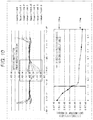
- the upper part of FIG. 10 illustrates a difference in application unevenness film thickness at the position indicated by the dotted line, which is in the region illustrated in the lower leftmost part in FIG. 9 in a case where the gap width d is varied to eight kinds of values of 0, 0.1, 0.15, 0.2, 0.25, 0.5, 0.75, and 1.0.
- the lower part of FIG. 10 illustrates an absolute value distribution of the difference in application unevenness film thickness in the upper part of FIG. 10 with respect to the gap width d.
- the imaging surface 21 a that is the range on the right side in the drawing, the region in which the flow velocity becomes lower than that in the periphery is generated so that the photoresist 12 is difficult to flow in the region in which the flow velocity becomes lower, and the like, whereby the film thickness of the photoresist film 12 a corresponding to the region is made thin, and the difference in application unevenness film thickness tends to be large.
- the flow velocity distribution becomes substantially uniform, whereby the absolute value of the difference in application unevenness film thickness tends to converge to a predetermined value (e.g., about 50 nm).
- the gap width d is larger than about 0.2
- the occurrence of the application unevenness is considered to be substantially suppressed. Accordingly, by configuring the cavity 61 such that the gap width d becomes larger than 0.2, a decrease in imaging characteristics caused by the application unevenness is suppressed and a decrease in a yield can be suppressed.
- the upper part of FIG. 11 illustrates a flow velocity distribution in a case where the gap width d is kept constant and a planer shape of the cavity 61 is, from the left in the drawing, square (Square), hexagonal (Penta), octagonal (Octa), and circular (Circle). Furthermore, the lower part of FIG. 11 illustrates a coating film thickness distribution of the respective photoresist layers 12 a in the range of the imaging surface 21 a indicated by the dotted line in the upper left part of FIG. 11 .
- the upper and lower parts of FIG. 11 indicate that the flow velocity distribution and the coating film thickness distribution are substantially the same in any planer shape.
- FIG. 12 illustrates a flow velocity distribution in a case substantially similar to the case where the size of the cavity 61 is varied to 10 ⁇ m ⁇ 10 ⁇ m (Square_Scale ⁇ 1), 50 ⁇ m ⁇ 50 ⁇ m (Square_Scale ⁇ 5), 100 ⁇ m ⁇ 100 ⁇ m (Square_Scale ⁇ 10), and 200 ⁇ m ⁇ 200 ⁇ m (Square_Scale ⁇ 20) by varying the viscosity of the photoresist 12 to 6 cP, 30 cP, 60 cP, and 120 cP with respect to the cavity 61 of 10 ⁇ m ⁇ 10 ⁇ m.
- FIG. 12 illustrates a coating film thickness distribution at the position corresponding to the dotted line portion indicated by the upper leftmost part of FIG. 12 in a case where substantially the size of the cavity 61 is varied to 10 ⁇ m ⁇ 10 ⁇ m (Square_Scale ⁇ 1), 20 ⁇ m ⁇ 20 ⁇ m (Square_Scale ⁇ 2), 30 ⁇ m ⁇ 30 ⁇ m (Square_Scale ⁇ 3), 40 ⁇ m ⁇ 40 ⁇ m (Square_Scale ⁇ 4), 50 ⁇ m ⁇ 50 ⁇ m (Square_Scale ⁇ 5), 60 ⁇ m ⁇ 60 ⁇ m (Square_Scale ⁇ 6), 80 ⁇ m ⁇ 80 ⁇ m (Square_Scale ⁇ 8), 100 ⁇ m ⁇ 100 ⁇ m (Square_Scale ⁇ 10), 200 ⁇ m ⁇ 200 ⁇ m (Square_Scale ⁇ 20), 400 ⁇ m ⁇ 400 ⁇ m (Square_Scale ⁇ 40),
- the flow velocity distribution is kept uniform throughout the region on the imaging surface 21 a right side of the range in which the cavity 61 is provided substantially up to the vicinity of the size of about 100 ⁇ m ⁇ 100 ⁇ m (Square_Scale ⁇ 10) with respect to the size of the cavity 61 .
- the flow velocity distribution is not in the uniform state with stripes in the lateral direction throughout the region on the imaging surface 21 a right side of the range in which the cavity 61 is provided in the case of the size of 200 ⁇ m ⁇ 200 ⁇ m (Square_Scale ⁇ 20).
- the coating film thickness converges to a predetermined thickness and is stabilized on the imaging surface 21 a right side of the range in which the cavity 61 is provided substantially up to the vicinity of the size of about 100 ⁇ m ⁇ 100 ⁇ m (Square_Scale ⁇ 10) with respect to the size of the cavity 61 .
- the coating film thickness enters an unstable wavy state throughout the region in the vertical direction (Y direction) in the drawing on the imaging surface 21 a right side of the range in which the cavity 61 is provided.
- the coating film thickness converges to a predetermined thickness and is stabilized on the imaging surface 21 a right side of the range in which the cavity 61 is provided substantially up to the vicinity of the size of about 100 ⁇ m ⁇ 100 ⁇ m (Square_Scale ⁇ 10) with respect to the size of the cavity 61 , whereby optical characteristics of the imaging sensor are maintained and a decrease in a yield can be suppressed.
- FIG. 13 illustrates a flow velocity distribution in a case substantially similar to the case where the size of the cavity 61 is varied to 10 ⁇ m ⁇ 10 ⁇ m (Square_Scale ⁇ 1), 50 ⁇ m ⁇ 50 ⁇ m (Square_Scale ⁇ 5), 200 ⁇ m ⁇ 200 ⁇ m (Square_Scale ⁇ 20), and 1000 ⁇ m ⁇ 1000 ⁇ m (Square_Scale ⁇ 100) by varying the acceleration level of flowing the photoresist 12 to 5 ⁇ 10 6 cm/sect, 1 ⁇ 10 6 cm/sect, 2.5 ⁇ 10 5 cm/sect, and 5 ⁇ 10 3 cm/sect with respect to the cavity 61 of 10 ⁇ m ⁇ 10 ⁇ m.
- FIG. 13 illustrates a coating film thickness distribution at the position corresponding to the dotted line portion indicated by the upper leftmost part of FIG. 13 in a case where substantially the size of the cavity 61 is varied to 10 ⁇ m ⁇ 10 ⁇ m (Square_Scale ⁇ 1), 20 ⁇ m ⁇ 20 ⁇ m (Square_Scale ⁇ 2), 30 ⁇ m ⁇ 30 ⁇ m (Square_Scale ⁇ 3), 40 ⁇ m ⁇ 40 ⁇ m (Square_Scale ⁇ 4), 50 ⁇ m ⁇ 50 ⁇ m (Square_Scale ⁇ 5), 60 ⁇ m ⁇ 60 ⁇ m (Square_Scale ⁇ 6), 80 ⁇ m ⁇ 80 ⁇ m (Square_Scale ⁇ 8), 100 ⁇ m ⁇ 100 ⁇ m (Square_Scale ⁇ 10), 200 ⁇ m ⁇ 200 ⁇ m (Square_Scale ⁇ 20), 400 ⁇ m ⁇ 400 ⁇ m (Square_Scale ⁇ 40),
- the flow velocity distribution is kept uniform throughout the region on the imaging surface 21 a right side of the range in which the cavity 61 is provided substantially up to the vicinity of the size of about 200 ⁇ m ⁇ 200 ⁇ m (Square_Scale ⁇ 20) with respect to the size of the cavity 61 .
- the flow velocity distribution is not in the uniform state with stripes in the lateral direction throughout the region on the imaging surface 21 a right side of the range in which the cavity 61 is provided in the case of the size of 1000 ⁇ m ⁇ 1000 ⁇ m (Square_Scale ⁇ 100).
- the coating film thickness converges to a predetermined thickness and is stabilized on the imaging surface 21 a right side of the range in which the cavity 61 is provided substantially up to the vicinity of the size of about 200 ⁇ m ⁇ 200 ⁇ m (Square_Scale ⁇ 10) with respect to the size of the cavity 61 .
- the coating film thickness enters an unstable wavy state throughout the region in the vertical direction (Y direction) in the drawing on the imaging surface 21 a right side of the range in which the cavity 61 is provided.
- the coating film thickness converges to a predetermined thickness and is stabilized on the imaging surface 21 a right side of the range in which the cavity 61 is provided substantially up to the vicinity of the size of about 200 ⁇ m ⁇ 200 ⁇ m (Square_Scale ⁇ 20) with respect to the size of the cavity 61 , whereby optical characteristics of the imaging sensor are maintained and a decrease in a yield can be suppressed.
- the flow velocity distribution of the photoresist 12 is stabilized up to the vicinity of the size of about 100 ⁇ m ⁇ 100 ⁇ m (Square_Scale ⁇ 10) with respect to the size of the cavity 61 , and in the case of varying the acceleration level of flowing the photoresist 12 , the flow velocity distribution of the photoresist 12 is stabilized up to the vicinity of the size of about 200 ⁇ m ⁇ 100 ⁇ m (Square_Scale ⁇ 20) with respect to the size of the cavity 61 .
- the flow velocity distribution of the photoresist 12 is stabilized up to the vicinity of the size of about 100 ⁇ m ⁇ 100 ⁇ m (Square_Scale ⁇ 10) with respect to the size of the cavity 61 in the substrate planar direction.
- the upper part of FIG. 14 illustrates a height of the coating film thickness in the horizontal direction indicated by the dotted line in the upper leftmost part of the lower part of FIG. 14 in a case where the photoresist 12 flows by varying the acceleration level from the left to the right in the drawing at the corner portion in which the cavity 61 having the step height of the film thickness of 1 ⁇ m is linearly disposed around the imaging surface 21 a at a predetermined pitch in the lower part of FIG. 14 .
- the lower part of FIG. 14 illustrates a flow velocity distribution for each acceleration level of making the photoresist 12 flow.
- the acceleration level is, in order from the upper leftmost part to the right of the lower part of FIG. 14 , 1.0 ⁇ 10 6 cm/sec 2 (acc 1.0 ⁇ 10 ⁇ circumflex over ( ) ⁇ 6), 2.5 ⁇ 10 6 cm/sec 2 (acc 2.5 ⁇ 10 ⁇ circumflex over ( ) ⁇ 6) 5.0 ⁇ 10 6 cm/sec 2 (acc 5.0 ⁇ 10 ⁇ circumflex over ( ) ⁇ 6), 7.5 ⁇ 10 6 cm/sec 2 (acc 7.5 ⁇ 10 ⁇ circumflex over ( ) ⁇ 6), 1.0 ⁇ 10 7 cm/sec 2 (acc 2.5 ⁇ 10 ⁇ circumflex over ( ) ⁇ 7), 2.5 ⁇ 10 7 cm/sec 2 (acc 2.5 ⁇ 10 ⁇ circumflex over ( ) ⁇ 7), 5.0 ⁇ 10 7 cm/sec 2 (acc 5.0 ⁇ 10 ⁇ circumflex over ( ) ⁇ 7), 7.5 ⁇ 10 7 cm/sec 2 (acc 7.5 ⁇ 10 ⁇ circumflex over ( ) ⁇ 7), 1.0 ⁇ 10 8 cm/sec 2 (acc 2.5 ⁇ 10 ⁇ circumflex over ( ) ⁇ 8),
- FIG. 14 illustrates the height of the coating film thickness for each acceleration level described above.
- the acceleration level of the photoresist 12 is larger than the acceleration level of 2.5 ⁇ 10 6 cm/sec 2 (acc 2.5 ⁇ 10 ⁇ circumflex over ( ) ⁇ 6)
- the outer shape of the application unevenness is present on the imaging surface 21 a , and the effect of the cavity 61 is generated.
- the effect of the cavity 61 can be considered to be generated.
- the coating film thickness of a case where the acceleration level of the photoresist 12 is 1.0 ⁇ 10 6 cm/sec 2 (acc 1.0 ⁇ 10 ⁇ circumflex over ( ) ⁇ 6) is about 5 ⁇ m.
- the coating film thickness can be set to a predetermined thickness on the imaging surface 21 a right side of the range in which the cavity 61 is provided, whereby a decrease in optical characteristics of the imaging sensor are suppressed and a decrease in a yield can be suppressed.
- the solid-state image sensor 21 described above can be applied to various electronic apparatuses such as an imaging device such as a digital still camera and a digital video camera, a mobile phone having an imaging function, and other devices having an imaging function.
- FIG. 15 is a block diagram illustrating an exemplary configuration of an imaging device as an electronic apparatus to which the present technology is applied.
- An imaging device 201 illustrated in FIG. 15 includes an optical system 202 , a shutter device 203 , a solid-state image sensor 204 , a drive circuit 205 , a signal processing circuit 206 , a monitor 207 , and a memory 208 , and is capable of capturing a still image and a moving image.
- the optical system 202 includes one or a plurality of lenses, guides light (incident light) from an object to the solid-state image sensor 204 , and forms an image on a light receiving surface of the solid-state image sensor 204 .
- the shutter device 203 is disposed between the optical system 202 and the solid-state image sensor 204 , and controls a light irradiation period and a light shading period with respect to the solid-state image sensor 204 under control of a drive circuit 1005 .
- the solid-state image sensor 204 includes a package including the above-described solid-state image sensor.
- the solid-state image sensor 204 accumulates signal charges for a certain period of time in accordance with the light for forming an image on the light receiving surface via the optical system 202 and the shutter device 203 .
- the signal charges accumulated in the solid-state image sensor 204 are transmitted in accordance with a drive signal (timing signal) supplied from the drive circuit 205 .
- the drive circuit 205 outputs the drive signal for controlling transfer operation of the solid-state image sensor 204 and shutter operation of the shutter device 203 , thereby driving the solid-state image sensor 204 and the shutter device 203 .
- the signal processing circuit 206 performs various signal processing on the signal charge output from the solid-state image sensor 204 .
- An image (image data) obtained by applying the signal processing performed by the signal processing circuit 206 is supplied to the monitor 207 and displayed, or supplied to the memory 208 and stored (recorded).
- FIG. 16 is a diagram illustrating an exemplary use of the solid-state image sensor 21 described above.
- the above-described image sensor can be used in various cases for sensing light such as visible light, infrared light, ultraviolet light, an X-ray, and the like, as exemplified below.
- a device for capturing an image to be used for viewing such as a digital camera and a mobile device with a camera function
- a device for the use of transit such as an on-vehicle sensor for capturing a front side, a rear side, surroundings, inside, and the like of a vehicle for the purpose of safe driving such as an automatic stop, recognition of a driver's condition, and the like, a monitoring camera for monitoring a traveling vehicle and a road, and a ranging sensor for measuring a distance between vehicles and the like
- a device for the use of home electric appliances for capturing a gesture of a user and performing device operation in accordance with the gesture such as a TV, a refrigerator, and an air conditioner
- a device for a healthcare and medical use such as an endoscope and a device for performing angiography based on infrared light reception
- a device for the use of security such as an anti-crime monitoring camera and a camera for authenticating a person
- a device for the use of beauty purpose such as a skin measuring device for photographing a skin and a microscope for photographing a scalp
- a device for the use of sports such as an action camera and a wearable camera for a sports use and the like
- a step structure on a substrate surface is in a divided state.
- the step structure on the substrate surface is in a state divided into the same shape.
- the step structure in the divided state includes a gap of a predetermined width.
- the predetermined width of the gap is larger than 0.2 in a case where a size of the divided step structure in a planar direction is set to 1.
- the step structure in the divided state is geometrically disposed with the predetermined width of the gap with respect to one predetermined axial direction.
- the step structure in the divided state is geometrically disposed with the predetermined width of the gap with respect to the one predetermined axial direction in such a manner that, in a case where fluid is dropped onto the substrate surface in a state where a wafer on which a plurality of solid-state image sensors is formed is rotated so that the fluid flows on the substrate surface, fluid velocities varied by the gap due to the step structure are cancelled out as a whole.
- a plurality of the step structures in the divided state is geometrically disposed on a two-dimensional plane with the predetermined width of the gap with respect to the one predetermined axial direction.
- the plurality of step structures in the divided state is geometrically disposed on the two-dimensional plane with the predetermined width of the gap with respect to the one predetermined axial direction in such a manner that, in a case where fluid is dropped onto the substrate surface in a state where a wafer on which the plurality of solid-state image sensors is formed is rotated so that the fluid flows on the substrate surface, fluid velocities varied by the gap due to the step structure are cancelled out as a whole.
- a size of the step structure in the divided state in a substrate planar direction is smaller than 100 ⁇ m.
- ⁇ 10> The solid-state image sensor according to any one of ⁇ 1> to ⁇ 9>, in which film thickness/height as a ratio between a film thickness of the fluid and a height of the substrate at a time when the fluid is dropped onto the substrate surface in the state where the wafer on which the plurality of solid-state image sensors is formed is rotated so that the fluid flows on the substrate surface is smaller than 5.
- a step structure on a substrate surface is in a divided state.
- a step structure on a substrate surface is in a divided state.
- a step structure on a substrate surface is in a divided state.
- a step structure on a substrate surface is in a divided state.
- a step structure on a substrate surface is in a divided state.
Landscapes
- Physics & Mathematics (AREA)
- General Physics & Mathematics (AREA)
- Solid State Image Pick-Up Elements (AREA)
- Engineering & Computer Science (AREA)
- Condensed Matter Physics & Semiconductors (AREA)
- Manufacturing & Machinery (AREA)
- Computer Hardware Design (AREA)
- Microelectronics & Electronic Packaging (AREA)
- Power Engineering (AREA)
Abstract
Description
- Patent Document 1: International Publication No. 2014/156657
- Patent Document 2: International Publication No. 2015/133324
- 11 Wafer
- 12 Photoresist
- 12 a Photoresist layer
- 21 Solid-state image sensor
- 21 a Imaging surface
- 31 Photoelectric conversion layer
- 32 Wiring layer
- 33 Logic layer
- 33 a Metal pad
- 41 Electrode
- 51 Cavity
- 61, and 61-1 to 61-n Cavity
- 71, and 71-1 to 71-4 Wiring
- 91, and 91-1 to 91-4 Wiring
Claims (13)
Applications Claiming Priority (3)
| Application Number | Priority Date | Filing Date | Title |
|---|---|---|---|
| JP2016-065605 | 2016-03-29 | ||
| JP2016065605A JP2017183387A (en) | 2016-03-29 | 2016-03-29 | Circuit board, semiconductor device, imaging device, solid-state imaging device, manufacturing method of solid-state imaging device, and electronic apparatus |
| PCT/JP2017/010300 WO2017169753A1 (en) | 2016-03-29 | 2017-03-15 | Circuit board, semiconductor device, image capturing device, solid-state image capturing element, method of manufacturing solid-state image capturing element, and electronic instrument |
Publications (2)
| Publication Number | Publication Date |
|---|---|
| US20190109168A1 US20190109168A1 (en) | 2019-04-11 |
| US10714524B2 true US10714524B2 (en) | 2020-07-14 |
Family
ID=59965215
Family Applications (1)
| Application Number | Title | Priority Date | Filing Date |
|---|---|---|---|
| US16/086,904 Expired - Fee Related US10714524B2 (en) | 2016-03-29 | 2017-03-15 | Circuit board, semiconductor device, imaging device, solid-state image sensor, method for manufacturing solid-state image sensor, and electronic apparatus |
Country Status (4)
| Country | Link |
|---|---|
| US (1) | US10714524B2 (en) |
| JP (1) | JP2017183387A (en) |
| CN (1) | CN108780804B (en) |
| WO (1) | WO2017169753A1 (en) |
Families Citing this family (1)
| Publication number | Priority date | Publication date | Assignee | Title |
|---|---|---|---|---|
| JP7462263B2 (en) * | 2020-03-24 | 2024-04-05 | パナソニックIpマネジメント株式会社 | Semiconductor element and solid-state imaging device |
Citations (9)
| Publication number | Priority date | Publication date | Assignee | Title |
|---|---|---|---|---|
| US4659226A (en) * | 1985-12-04 | 1987-04-21 | Rca Corporation | Method of making a semiconductor device |
| US6030880A (en) * | 1998-04-03 | 2000-02-29 | Sony Corporation Of Japan | Alignment feature that avoids comet tail formation in spin-on materials and production method therefor |
| JP2007005384A (en) | 2005-06-21 | 2007-01-11 | Sharp Corp | SEMICONDUCTOR DEVICE, ITS MANUFACTURING METHOD, AND ELECTRONIC INFORMATION DEVICE |
| US7736938B2 (en) * | 2007-12-28 | 2010-06-15 | Dongbu Hitek Co., Ltd | Methods for fabricating CMOS image sensor |
| JP2011086658A (en) | 2009-10-13 | 2011-04-28 | Fujifilm Corp | Method of manufacturing solid-state imaging element, solid-state imaging element, and imaging device |
| US20130256824A1 (en) | 2012-04-02 | 2013-10-03 | Sony Corporation | Solid-state imaging device, method of manufacturing solid-state imaging device, apparatus for manufacturing semiconductor device, method of manufacturing semiconductor device, and electronic device |
| JP2013214616A (en) | 2012-04-02 | 2013-10-17 | Sony Corp | Solid-state imaging device, method of manufacturing solid-state imaging device, and electronic device |
| WO2014156657A1 (en) | 2013-03-25 | 2014-10-02 | ソニー株式会社 | Solid-state imaging device, production method therefor, and electronic device |
| WO2015133324A1 (en) | 2014-03-06 | 2015-09-11 | ソニー株式会社 | Solid-state imaging device, method for manufacturing same and electronic device |
Family Cites Families (9)
| Publication number | Priority date | Publication date | Assignee | Title |
|---|---|---|---|---|
| JP2001189286A (en) * | 1999-12-28 | 2001-07-10 | Sony Corp | Solid-state imaging device and method of manufacturing the same |
| CN1875617A (en) * | 2003-10-27 | 2006-12-06 | 皇家飞利浦电子股份有限公司 | Camera module and manufacturing method for such a camera module |
| TW200528756A (en) * | 2004-01-27 | 2005-09-01 | Adv Lcd Tech Dev Ct Co Ltd | Light application apparatus, crystallization apparatus and optical modulation element assembly |
| JP4762729B2 (en) * | 2006-01-13 | 2011-08-31 | シャープ株式会社 | Mounting structure of semiconductor laser element |
| JP2009266900A (en) * | 2008-04-22 | 2009-11-12 | Panasonic Corp | Solid-state image sensor |
| JP2011060974A (en) * | 2009-09-09 | 2011-03-24 | Canon Inc | Solid-state image pickup device and digital camera |
| JP2011088658A (en) * | 2009-10-26 | 2011-05-06 | Nifco Inc | Lid opening device of container |
| JP2012049401A (en) * | 2010-08-27 | 2012-03-08 | Canon Inc | Method of manufacturing photosensor |
| CN204009300U (en) * | 2014-07-18 | 2014-12-10 | 广西钦州天山微电子有限公司 | The vertical orientation type LCD liquid crystal display of step width >=2.5mm |
-
2016
- 2016-03-29 JP JP2016065605A patent/JP2017183387A/en active Pending
-
2017
- 2017-03-15 CN CN201780019353.8A patent/CN108780804B/en active Active
- 2017-03-15 WO PCT/JP2017/010300 patent/WO2017169753A1/en not_active Ceased
- 2017-03-15 US US16/086,904 patent/US10714524B2/en not_active Expired - Fee Related
Patent Citations (10)
| Publication number | Priority date | Publication date | Assignee | Title |
|---|---|---|---|---|
| US4659226A (en) * | 1985-12-04 | 1987-04-21 | Rca Corporation | Method of making a semiconductor device |
| US6030880A (en) * | 1998-04-03 | 2000-02-29 | Sony Corporation Of Japan | Alignment feature that avoids comet tail formation in spin-on materials and production method therefor |
| JP2007005384A (en) | 2005-06-21 | 2007-01-11 | Sharp Corp | SEMICONDUCTOR DEVICE, ITS MANUFACTURING METHOD, AND ELECTRONIC INFORMATION DEVICE |
| US7736938B2 (en) * | 2007-12-28 | 2010-06-15 | Dongbu Hitek Co., Ltd | Methods for fabricating CMOS image sensor |
| JP2011086658A (en) | 2009-10-13 | 2011-04-28 | Fujifilm Corp | Method of manufacturing solid-state imaging element, solid-state imaging element, and imaging device |
| US20130256824A1 (en) | 2012-04-02 | 2013-10-03 | Sony Corporation | Solid-state imaging device, method of manufacturing solid-state imaging device, apparatus for manufacturing semiconductor device, method of manufacturing semiconductor device, and electronic device |
| JP2013214616A (en) | 2012-04-02 | 2013-10-17 | Sony Corp | Solid-state imaging device, method of manufacturing solid-state imaging device, and electronic device |
| CN103367374A (en) | 2012-04-02 | 2013-10-23 | 索尼公司 | Solid-state imaging device, method of manufacturing solid-state imaging device, apparatus for manufacturing semiconductor device, method of manufacturing semiconductor device, and electronic device |
| WO2014156657A1 (en) | 2013-03-25 | 2014-10-02 | ソニー株式会社 | Solid-state imaging device, production method therefor, and electronic device |
| WO2015133324A1 (en) | 2014-03-06 | 2015-09-11 | ソニー株式会社 | Solid-state imaging device, method for manufacturing same and electronic device |
Non-Patent Citations (1)
| Title |
|---|
| International Search Report and Written Opinion of PCT Application No. PCT/JP2017/010300, dated Jun. 6, 2017, 10 pages of ISRWO. |
Also Published As
| Publication number | Publication date |
|---|---|
| US20190109168A1 (en) | 2019-04-11 |
| WO2017169753A1 (en) | 2017-10-05 |
| JP2017183387A (en) | 2017-10-05 |
| CN108780804A (en) | 2018-11-09 |
| CN108780804B (en) | 2022-12-16 |
Similar Documents
| Publication | Publication Date | Title |
|---|---|---|
| US11862656B2 (en) | Semiconductor device and manufacturing method, and electronic appliance | |
| US11043436B2 (en) | Semiconductor device, manufacturing method, imaging device, and electronic apparatus for enabling component mounting with high flatness | |
| EP3525239A1 (en) | Photoelectric conversion apparatus and equipment | |
| US10490586B2 (en) | Solid-state imaging device with light shielding films, method of manufacturing the same, and electronic apparatus | |
| WO2017126376A1 (en) | Image sensor, manufacturing method, and electronic device | |
| CN107534027B (en) | Semiconductor device, electronic device, and manufacturing method | |
| US12119366B2 (en) | Solid state imaging device, solid state imaging device manufacturing method, and electronic apparatus | |
| WO2017061273A1 (en) | Imaging device, manufacturing method | |
| CN109478555B (en) | Solid-state imaging element, manufacturing method, and electronic device | |
| TW202015195A (en) | Image sensor wafer level packaging | |
| US20160363673A1 (en) | Method of fabricating integrated digital x-ray image sensor, and integrated digital x-ray image sensor using the same | |
| US10714524B2 (en) | Circuit board, semiconductor device, imaging device, solid-state image sensor, method for manufacturing solid-state image sensor, and electronic apparatus | |
| US11482557B2 (en) | Solid-state image-capturing device, semiconductor apparatus, electronic apparatus, and manufacturing method | |
| CN111295762B (en) | Solid-state imaging element, manufacturing method, and electronic device | |
| WO2014156657A1 (en) | Solid-state imaging device, production method therefor, and electronic device | |
| US9941325B2 (en) | Method of manufacturing solid-state image sensor | |
| WO2025105260A1 (en) | Imaging device and electronic apparatus | |
| US10867856B2 (en) | Semiconductor device and method of manufacturing the same, and electronic apparatus | |
| US11041980B2 (en) | Solid-state imaging element, manufacturing method, and electronic device | |
| WO2020059237A1 (en) | Solid-state imaging device and electronic device |
Legal Events
| Date | Code | Title | Description |
|---|---|---|---|
| AS | Assignment |
Owner name: SONY CORPORATION, JAPAN Free format text: ASSIGNMENT OF ASSIGNORS INTEREST;ASSIGNOR:TAKEO, KENJI;REEL/FRAME:047117/0802 Effective date: 20180910 |
|
| FEPP | Fee payment procedure |
Free format text: ENTITY STATUS SET TO UNDISCOUNTED (ORIGINAL EVENT CODE: BIG.); ENTITY STATUS OF PATENT OWNER: LARGE ENTITY |
|
| STPP | Information on status: patent application and granting procedure in general |
Free format text: DOCKETED NEW CASE - READY FOR EXAMINATION |
|
| STPP | Information on status: patent application and granting procedure in general |
Free format text: NON FINAL ACTION MAILED |
|
| STPP | Information on status: patent application and granting procedure in general |
Free format text: RESPONSE TO NON-FINAL OFFICE ACTION ENTERED AND FORWARDED TO EXAMINER |
|
| STPP | Information on status: patent application and granting procedure in general |
Free format text: PUBLICATIONS -- ISSUE FEE PAYMENT VERIFIED |
|
| STCF | Information on status: patent grant |
Free format text: PATENTED CASE |
|
| FEPP | Fee payment procedure |
Free format text: MAINTENANCE FEE REMINDER MAILED (ORIGINAL EVENT CODE: REM.); ENTITY STATUS OF PATENT OWNER: LARGE ENTITY |
|
| LAPS | Lapse for failure to pay maintenance fees |
Free format text: PATENT EXPIRED FOR FAILURE TO PAY MAINTENANCE FEES (ORIGINAL EVENT CODE: EXP.); ENTITY STATUS OF PATENT OWNER: LARGE ENTITY |
|
| STCH | Information on status: patent discontinuation |
Free format text: PATENT EXPIRED DUE TO NONPAYMENT OF MAINTENANCE FEES UNDER 37 CFR 1.362 |
|
| FP | Lapsed due to failure to pay maintenance fee |
Effective date: 20240714 |