US10705278B2 - Backlight unit and display device including the same - Google Patents
Backlight unit and display device including the same Download PDFInfo
- Publication number
- US10705278B2 US10705278B2 US16/181,468 US201816181468A US10705278B2 US 10705278 B2 US10705278 B2 US 10705278B2 US 201816181468 A US201816181468 A US 201816181468A US 10705278 B2 US10705278 B2 US 10705278B2
- Authority
- US
- United States
- Prior art keywords
- light
- layer
- guide plate
- conversion layer
- predetermined wavelength
- Prior art date
- Legal status (The legal status is an assumption and is not a legal conclusion. Google has not performed a legal analysis and makes no representation as to the accuracy of the status listed.)
- Expired - Fee Related
Links
- 238000006243 chemical reaction Methods 0.000 claims abstract description 106
- 239000002096 quantum dot Substances 0.000 claims description 58
- 230000004888 barrier function Effects 0.000 claims description 40
- 238000007789 sealing Methods 0.000 claims description 11
- 239000011347 resin Substances 0.000 claims description 10
- 229920005989 resin Polymers 0.000 claims description 10
- 229910052782 aluminium Inorganic materials 0.000 claims description 8
- XAGFODPZIPBFFR-UHFFFAOYSA-N aluminium Chemical compound [Al] XAGFODPZIPBFFR-UHFFFAOYSA-N 0.000 claims description 8
- 239000011159 matrix material Substances 0.000 claims description 7
- 241000272470 Circus Species 0.000 claims description 2
- 239000000758 substrate Substances 0.000 description 18
- 239000000463 material Substances 0.000 description 16
- 239000004973 liquid crystal related substance Substances 0.000 description 8
- VYPSYNLAJGMNEJ-UHFFFAOYSA-N Silicium dioxide Chemical compound O=[Si]=O VYPSYNLAJGMNEJ-UHFFFAOYSA-N 0.000 description 6
- 229910010272 inorganic material Inorganic materials 0.000 description 6
- 239000011147 inorganic material Substances 0.000 description 6
- 229910052751 metal Inorganic materials 0.000 description 6
- 239000002184 metal Substances 0.000 description 6
- 229910052814 silicon oxide Inorganic materials 0.000 description 6
- QVGXLLKOCUKJST-UHFFFAOYSA-N atomic oxygen Chemical compound [O] QVGXLLKOCUKJST-UHFFFAOYSA-N 0.000 description 5
- 238000004519 manufacturing process Methods 0.000 description 5
- 229910052760 oxygen Inorganic materials 0.000 description 5
- 239000001301 oxygen Substances 0.000 description 5
- 239000011248 coating agent Substances 0.000 description 3
- 238000000576 coating method Methods 0.000 description 3
- 239000000203 mixture Substances 0.000 description 3
- 150000004767 nitrides Chemical class 0.000 description 3
- 239000011368 organic material Substances 0.000 description 3
- 239000003086 colorant Substances 0.000 description 2
- 238000003475 lamination Methods 0.000 description 2
- 238000000034 method Methods 0.000 description 2
- 229910052755 nonmetal Inorganic materials 0.000 description 2
- 238000001429 visible spectrum Methods 0.000 description 2
- 241001085205 Prenanthella exigua Species 0.000 description 1
- 238000010276 construction Methods 0.000 description 1
- 239000002274 desiccant Substances 0.000 description 1
- 230000006866 deterioration Effects 0.000 description 1
- -1 e.g. Substances 0.000 description 1
- 230000005684 electric field Effects 0.000 description 1
- 230000005611 electricity Effects 0.000 description 1
- 230000004313 glare Effects 0.000 description 1
- 239000002159 nanocrystal Substances 0.000 description 1
- 239000010409 thin film Substances 0.000 description 1
- 238000002834 transmittance Methods 0.000 description 1
Images


Classifications
-
- G—PHYSICS
- G02—OPTICS
- G02B—OPTICAL ELEMENTS, SYSTEMS OR APPARATUS
- G02B6/00—Light guides; Structural details of arrangements comprising light guides and other optical elements, e.g. couplings
- G02B6/0001—Light guides; Structural details of arrangements comprising light guides and other optical elements, e.g. couplings specially adapted for lighting devices or systems
- G02B6/0011—Light guides; Structural details of arrangements comprising light guides and other optical elements, e.g. couplings specially adapted for lighting devices or systems the light guides being planar or of plate-like form
- G02B6/0013—Means for improving the coupling-in of light from the light source into the light guide
- G02B6/0023—Means for improving the coupling-in of light from the light source into the light guide provided by one optical element, or plurality thereof, placed between the light guide and the light source, or around the light source
- G02B6/0026—Wavelength selective element, sheet or layer, e.g. filter or grating
-
- G—PHYSICS
- G02—OPTICS
- G02B—OPTICAL ELEMENTS, SYSTEMS OR APPARATUS
- G02B6/00—Light guides; Structural details of arrangements comprising light guides and other optical elements, e.g. couplings
- G02B6/0001—Light guides; Structural details of arrangements comprising light guides and other optical elements, e.g. couplings specially adapted for lighting devices or systems
- G02B6/0011—Light guides; Structural details of arrangements comprising light guides and other optical elements, e.g. couplings specially adapted for lighting devices or systems the light guides being planar or of plate-like form
- G02B6/0033—Means for improving the coupling-out of light from the light guide
- G02B6/005—Means for improving the coupling-out of light from the light guide provided by one optical element, or plurality thereof, placed on the light output side of the light guide
- G02B6/0055—Reflecting element, sheet or layer
-
- G—PHYSICS
- G02—OPTICS
- G02B—OPTICAL ELEMENTS, SYSTEMS OR APPARATUS
- G02B6/00—Light guides; Structural details of arrangements comprising light guides and other optical elements, e.g. couplings
- G02B6/0001—Light guides; Structural details of arrangements comprising light guides and other optical elements, e.g. couplings specially adapted for lighting devices or systems
- G02B6/0011—Light guides; Structural details of arrangements comprising light guides and other optical elements, e.g. couplings specially adapted for lighting devices or systems the light guides being planar or of plate-like form
- G02B6/0013—Means for improving the coupling-in of light from the light source into the light guide
- G02B6/0023—Means for improving the coupling-in of light from the light source into the light guide provided by one optical element, or plurality thereof, placed between the light guide and the light source, or around the light source
- G02B6/0031—Reflecting element, sheet or layer
-
- G—PHYSICS
- G02—OPTICS
- G02B—OPTICAL ELEMENTS, SYSTEMS OR APPARATUS
- G02B6/00—Light guides; Structural details of arrangements comprising light guides and other optical elements, e.g. couplings
- G02B6/0001—Light guides; Structural details of arrangements comprising light guides and other optical elements, e.g. couplings specially adapted for lighting devices or systems
- G02B6/0011—Light guides; Structural details of arrangements comprising light guides and other optical elements, e.g. couplings specially adapted for lighting devices or systems the light guides being planar or of plate-like form
- G02B6/0033—Means for improving the coupling-out of light from the light guide
- G02B6/005—Means for improving the coupling-out of light from the light guide provided by one optical element, or plurality thereof, placed on the light output side of the light guide
-
- G—PHYSICS
- G02—OPTICS
- G02B—OPTICAL ELEMENTS, SYSTEMS OR APPARATUS
- G02B6/00—Light guides; Structural details of arrangements comprising light guides and other optical elements, e.g. couplings
- G02B6/0001—Light guides; Structural details of arrangements comprising light guides and other optical elements, e.g. couplings specially adapted for lighting devices or systems
- G02B6/0011—Light guides; Structural details of arrangements comprising light guides and other optical elements, e.g. couplings specially adapted for lighting devices or systems the light guides being planar or of plate-like form
- G02B6/0033—Means for improving the coupling-out of light from the light guide
- G02B6/0058—Means for improving the coupling-out of light from the light guide varying in density, size, shape or depth along the light guide
-
- G—PHYSICS
- G02—OPTICS
- G02B—OPTICAL ELEMENTS, SYSTEMS OR APPARATUS
- G02B6/00—Light guides; Structural details of arrangements comprising light guides and other optical elements, e.g. couplings
- G02B6/0001—Light guides; Structural details of arrangements comprising light guides and other optical elements, e.g. couplings specially adapted for lighting devices or systems
- G02B6/0011—Light guides; Structural details of arrangements comprising light guides and other optical elements, e.g. couplings specially adapted for lighting devices or systems the light guides being planar or of plate-like form
- G02B6/0066—Light guides; Structural details of arrangements comprising light guides and other optical elements, e.g. couplings specially adapted for lighting devices or systems the light guides being planar or of plate-like form characterised by the light source being coupled to the light guide
- G02B6/0068—Arrangements of plural sources, e.g. multi-colour light sources
-
- G—PHYSICS
- G02—OPTICS
- G02B—OPTICAL ELEMENTS, SYSTEMS OR APPARATUS
- G02B6/00—Light guides; Structural details of arrangements comprising light guides and other optical elements, e.g. couplings
- G02B6/0001—Light guides; Structural details of arrangements comprising light guides and other optical elements, e.g. couplings specially adapted for lighting devices or systems
- G02B6/0011—Light guides; Structural details of arrangements comprising light guides and other optical elements, e.g. couplings specially adapted for lighting devices or systems the light guides being planar or of plate-like form
- G02B6/0066—Light guides; Structural details of arrangements comprising light guides and other optical elements, e.g. couplings specially adapted for lighting devices or systems the light guides being planar or of plate-like form characterised by the light source being coupled to the light guide
- G02B6/0073—Light emitting diode [LED]
-
- G—PHYSICS
- G02—OPTICS
- G02F—OPTICAL DEVICES OR ARRANGEMENTS FOR THE CONTROL OF LIGHT BY MODIFICATION OF THE OPTICAL PROPERTIES OF THE MEDIA OF THE ELEMENTS INVOLVED THEREIN; NON-LINEAR OPTICS; FREQUENCY-CHANGING OF LIGHT; OPTICAL LOGIC ELEMENTS; OPTICAL ANALOGUE/DIGITAL CONVERTERS
- G02F1/00—Devices or arrangements for the control of the intensity, colour, phase, polarisation or direction of light arriving from an independent light source, e.g. switching, gating or modulating; Non-linear optics
- G02F1/01—Devices or arrangements for the control of the intensity, colour, phase, polarisation or direction of light arriving from an independent light source, e.g. switching, gating or modulating; Non-linear optics for the control of the intensity, phase, polarisation or colour
- G02F1/13—Devices or arrangements for the control of the intensity, colour, phase, polarisation or direction of light arriving from an independent light source, e.g. switching, gating or modulating; Non-linear optics for the control of the intensity, phase, polarisation or colour based on liquid crystals, e.g. single liquid crystal display cells
- G02F1/133—Constructional arrangements; Operation of liquid crystal cells; Circuit arrangements
- G02F1/1333—Constructional arrangements; Manufacturing methods
- G02F1/1335—Structural association of cells with optical devices, e.g. polarisers or reflectors
- G02F1/133553—Reflecting elements
-
- G—PHYSICS
- G02—OPTICS
- G02F—OPTICAL DEVICES OR ARRANGEMENTS FOR THE CONTROL OF LIGHT BY MODIFICATION OF THE OPTICAL PROPERTIES OF THE MEDIA OF THE ELEMENTS INVOLVED THEREIN; NON-LINEAR OPTICS; FREQUENCY-CHANGING OF LIGHT; OPTICAL LOGIC ELEMENTS; OPTICAL ANALOGUE/DIGITAL CONVERTERS
- G02F1/00—Devices or arrangements for the control of the intensity, colour, phase, polarisation or direction of light arriving from an independent light source, e.g. switching, gating or modulating; Non-linear optics
- G02F1/01—Devices or arrangements for the control of the intensity, colour, phase, polarisation or direction of light arriving from an independent light source, e.g. switching, gating or modulating; Non-linear optics for the control of the intensity, phase, polarisation or colour
- G02F1/13—Devices or arrangements for the control of the intensity, colour, phase, polarisation or direction of light arriving from an independent light source, e.g. switching, gating or modulating; Non-linear optics for the control of the intensity, phase, polarisation or colour based on liquid crystals, e.g. single liquid crystal display cells
- G02F1/133—Constructional arrangements; Operation of liquid crystal cells; Circuit arrangements
- G02F1/1333—Constructional arrangements; Manufacturing methods
- G02F1/1335—Structural association of cells with optical devices, e.g. polarisers or reflectors
- G02F1/1336—Illuminating devices
- G02F1/133602—Direct backlight
- G02F1/133605—Direct backlight including specially adapted reflectors
-
- G—PHYSICS
- G02—OPTICS
- G02F—OPTICAL DEVICES OR ARRANGEMENTS FOR THE CONTROL OF LIGHT BY MODIFICATION OF THE OPTICAL PROPERTIES OF THE MEDIA OF THE ELEMENTS INVOLVED THEREIN; NON-LINEAR OPTICS; FREQUENCY-CHANGING OF LIGHT; OPTICAL LOGIC ELEMENTS; OPTICAL ANALOGUE/DIGITAL CONVERTERS
- G02F1/00—Devices or arrangements for the control of the intensity, colour, phase, polarisation or direction of light arriving from an independent light source, e.g. switching, gating or modulating; Non-linear optics
- G02F1/01—Devices or arrangements for the control of the intensity, colour, phase, polarisation or direction of light arriving from an independent light source, e.g. switching, gating or modulating; Non-linear optics for the control of the intensity, phase, polarisation or colour
- G02F1/13—Devices or arrangements for the control of the intensity, colour, phase, polarisation or direction of light arriving from an independent light source, e.g. switching, gating or modulating; Non-linear optics for the control of the intensity, phase, polarisation or colour based on liquid crystals, e.g. single liquid crystal display cells
- G02F1/133—Constructional arrangements; Operation of liquid crystal cells; Circuit arrangements
- G02F1/1333—Constructional arrangements; Manufacturing methods
- G02F1/1335—Structural association of cells with optical devices, e.g. polarisers or reflectors
- G02F1/1336—Illuminating devices
- G02F1/133602—Direct backlight
- G02F1/133606—Direct backlight including a specially adapted diffusing, scattering or light controlling members
-
- G—PHYSICS
- G02—OPTICS
- G02F—OPTICAL DEVICES OR ARRANGEMENTS FOR THE CONTROL OF LIGHT BY MODIFICATION OF THE OPTICAL PROPERTIES OF THE MEDIA OF THE ELEMENTS INVOLVED THEREIN; NON-LINEAR OPTICS; FREQUENCY-CHANGING OF LIGHT; OPTICAL LOGIC ELEMENTS; OPTICAL ANALOGUE/DIGITAL CONVERTERS
- G02F1/00—Devices or arrangements for the control of the intensity, colour, phase, polarisation or direction of light arriving from an independent light source, e.g. switching, gating or modulating; Non-linear optics
- G02F1/01—Devices or arrangements for the control of the intensity, colour, phase, polarisation or direction of light arriving from an independent light source, e.g. switching, gating or modulating; Non-linear optics for the control of the intensity, phase, polarisation or colour
- G02F1/13—Devices or arrangements for the control of the intensity, colour, phase, polarisation or direction of light arriving from an independent light source, e.g. switching, gating or modulating; Non-linear optics for the control of the intensity, phase, polarisation or colour based on liquid crystals, e.g. single liquid crystal display cells
- G02F1/133—Constructional arrangements; Operation of liquid crystal cells; Circuit arrangements
- G02F1/1333—Constructional arrangements; Manufacturing methods
- G02F1/1335—Structural association of cells with optical devices, e.g. polarisers or reflectors
- G02F1/1336—Illuminating devices
- G02F1/133602—Direct backlight
- G02F1/133606—Direct backlight including a specially adapted diffusing, scattering or light controlling members
- G02F1/133607—Direct backlight including a specially adapted diffusing, scattering or light controlling members the light controlling member including light directing or refracting elements, e.g. prisms or lenses
-
- G—PHYSICS
- G02—OPTICS
- G02F—OPTICAL DEVICES OR ARRANGEMENTS FOR THE CONTROL OF LIGHT BY MODIFICATION OF THE OPTICAL PROPERTIES OF THE MEDIA OF THE ELEMENTS INVOLVED THEREIN; NON-LINEAR OPTICS; FREQUENCY-CHANGING OF LIGHT; OPTICAL LOGIC ELEMENTS; OPTICAL ANALOGUE/DIGITAL CONVERTERS
- G02F1/00—Devices or arrangements for the control of the intensity, colour, phase, polarisation or direction of light arriving from an independent light source, e.g. switching, gating or modulating; Non-linear optics
- G02F1/01—Devices or arrangements for the control of the intensity, colour, phase, polarisation or direction of light arriving from an independent light source, e.g. switching, gating or modulating; Non-linear optics for the control of the intensity, phase, polarisation or colour
- G02F1/13—Devices or arrangements for the control of the intensity, colour, phase, polarisation or direction of light arriving from an independent light source, e.g. switching, gating or modulating; Non-linear optics for the control of the intensity, phase, polarisation or colour based on liquid crystals, e.g. single liquid crystal display cells
- G02F1/133—Constructional arrangements; Operation of liquid crystal cells; Circuit arrangements
- G02F1/1333—Constructional arrangements; Manufacturing methods
- G02F1/1335—Structural association of cells with optical devices, e.g. polarisers or reflectors
- G02F1/1336—Illuminating devices
- G02F1/133614—Illuminating devices using photoluminescence, e.g. phosphors illuminated by UV or blue light
-
- G—PHYSICS
- G02—OPTICS
- G02F—OPTICAL DEVICES OR ARRANGEMENTS FOR THE CONTROL OF LIGHT BY MODIFICATION OF THE OPTICAL PROPERTIES OF THE MEDIA OF THE ELEMENTS INVOLVED THEREIN; NON-LINEAR OPTICS; FREQUENCY-CHANGING OF LIGHT; OPTICAL LOGIC ELEMENTS; OPTICAL ANALOGUE/DIGITAL CONVERTERS
- G02F1/00—Devices or arrangements for the control of the intensity, colour, phase, polarisation or direction of light arriving from an independent light source, e.g. switching, gating or modulating; Non-linear optics
- G02F1/01—Devices or arrangements for the control of the intensity, colour, phase, polarisation or direction of light arriving from an independent light source, e.g. switching, gating or modulating; Non-linear optics for the control of the intensity, phase, polarisation or colour
- G02F1/13—Devices or arrangements for the control of the intensity, colour, phase, polarisation or direction of light arriving from an independent light source, e.g. switching, gating or modulating; Non-linear optics for the control of the intensity, phase, polarisation or colour based on liquid crystals, e.g. single liquid crystal display cells
- G02F1/133—Constructional arrangements; Operation of liquid crystal cells; Circuit arrangements
- G02F1/1333—Constructional arrangements; Manufacturing methods
- G02F1/1335—Structural association of cells with optical devices, e.g. polarisers or reflectors
- G02F1/1336—Illuminating devices
- G02F1/133616—Front illuminating devices
-
- G—PHYSICS
- G02—OPTICS
- G02F—OPTICAL DEVICES OR ARRANGEMENTS FOR THE CONTROL OF LIGHT BY MODIFICATION OF THE OPTICAL PROPERTIES OF THE MEDIA OF THE ELEMENTS INVOLVED THEREIN; NON-LINEAR OPTICS; FREQUENCY-CHANGING OF LIGHT; OPTICAL LOGIC ELEMENTS; OPTICAL ANALOGUE/DIGITAL CONVERTERS
- G02F2202/00—Materials and properties
- G02F2202/36—Micro- or nanomaterials
Definitions
- Embodiments of the inventive concept relate to a display device and ways to eliminate scattering patterns in a backlight unit. More particularly, embodiments of the inventive concept relate to the backlight unit including a reflective pattern layer and a display device including the backlight unit.
- a liquid crystal display is one of the most widely used display devices today because of their display quality, relatively thin screen size, and efficiency in terms of power usage.
- an LCD displays an image by holding a liquid crystal material between an upper substrate formed with common electrodes, color filters, and the like, and a lower substrate formed with thin film transistors, pixel electrodes, and the like, and applying different voltages to the pixel and common electrodes to generate an electric field.
- Application of different voltages to the pixel and common electrodes changes the arrangement of liquid crystal molecules, and thereby adjusts the transmittance of light.
- an LCD panel of the LCD is in itself a non-emissive type of light receiving element.
- an LCD generally includes a backlight unit for supplying light to the LCD panel that, for example, may serve as a source of light that may be reflected off liquid crystal material, and may provide a display having uniform brightness.
- a cold cathode fluorescent lamp (CCFL) has been widely used, because it consumes little power and provides bright white light.
- CCFL cold cathode fluorescent lamp
- LED light emitting diode
- the light conversion member may convert light having a predetermined color, and generated from a light source, into white light.
- the light conversion member may convert blue light generated from the light source into white light.
- the white light generated by the light conversion member may be provided to the LCD panel, and pixels of the LCD panel may display an image by using the white light provided from the light conversion member.
- An embodiment of the inventive concept is to provide a backlight unit providing light without scattering patterns.
- An embodiment of the inventive concept is to provide a display device including a backlight unit providing light for uniform display without using scattering patterns.
- a backlight unit may include a light source that emits light having a first predetermined wavelength; a light guide plate configured to guide light emitted from the light source; a light conversion layer disposed on the light guide plate; and a reflective pattern layer arranged between the light guide plate and the light conversion layer in which light traveling in the light guide plate is reflected by the reflective pattern layer, the reflective pattern layer including a plurality of holes, and wherein the light conversion layer absorbs at least a portion of the light emitted from the light source at the first predetermined wavelength and generates light having a second predetermined wavelength different than the first predetermined wavelength.
- the light conversion layer includes a plurality of quantum dots arranged in a resin.
- the plurality of quantum dots may include at least first quantum dots and second quantum dots being respectively sized to convert the light emitted from the light source at the first predetermined wavelength that enters the light conversion layer into the second predetermined wavelength or a third predetermined wavelength, respectively.
- the light emitted from the light source may be reflected by the reflective pattern layer.
- the light guided by the light guide plate may pass through the plurality of holes of the reflective pattern layer.
- the plurality of holes may be arranged as a matrix form in a plan view.
- the reflective pattern layer may include aluminum (Al).
- the light conversion layer may be configured to convert incident light that passes through the plurality of holes of the reflective pattern layer from the fight guide plate and has a first wavelength converted into light that has a second wavelength.
- the backlight unit may further include a reflective layer.
- the light conversion layer may be between the reflective pattern layer and the reflective layer.
- the light conversion layer may be configured to convert incident light that passes through the plurality of holes of the reflective pattern layer from the light guide plate and has a first wavelength into converted light that has a second wavelength.
- the converted light may be reflected by the reflective layer and passes through the plurality of holes of the reflective pattern layer.
- the backlight unit may further include a sealing member covering a side portion of the light conversion layer.
- the backlight unit may further include a barrier layer between the light conversion layer and the reflective pattern layer.
- a display device may include a display panel configured to display an image; and a backlight unit configured to provide light to the display panel, wherein the backlight unit includes: a light source that emits light having a first predetermined wavelength; a light guide plate configured to guide light emitted from the light source; a light conversion layer disposed on the light guide plate that absorbs at least a portion of the light emitted from the light source at the first predetermined wavelength and generates light having a second predetermined wavelength different than the first predetermined wavelength.
- a reflective pattern layer may be arranged between the light guide plate and the light conversion layer, in which light traveling in the light guide plate is reflected by the reflective pattern layer, and wherein the reflective pattern layer includes a plurality of holes arranged in a pattern.
- the light emitted from the light source may be reflected by the reflective pattern layer.
- the light guided by the light guide plate may pass through the plurality of holes of the reflective pattern layer.
- the plurality of holes may be arranged as a matrix form in a plan view.
- the light conversion layer may be between the display panel and the light guide plate.
- the light conversion layer may be configured to convert incident light that passes through the plurality of holes of the reflective pattern layer from the light guide plate and has a first wavelength into converted light that has a second wavelength.
- the converted light may be provided to the display panel.
- the light guide plate may be between the display panel and the light conversion layer.
- the backlight unit may further include a reflective layer.
- the light conversion layer may be between the reflective pattern layer and the reflective layer.
- the light conversion layer may be configured to convert incident light that passes through the plurality of holes of the reflective pattern layer from the light guide plate and has a first wavelength into converted light that has a second wavelength.
- the converted light may be reflected by the reflective layer and provided to the display panel by passing through the plurality of holes of the reflective pattern layer.
- the backlight unit may further include a sealing member covering a side portion of the light conversion layer.
- the backlight unit may include the reflective pattern layer including the plurality of holes between the light guide plate and the light conversion layer. Accordingly, the backlight unit may provide light without the scattering patterns. In addition, the backlight according to some embodiments of the inventive concept may provide light without a low refractive layer disposed on the light guide plate.
- the backlight unit of the display device may include the reflective pattern layer including the plurality of holes between the light guide plate and the light conversion layer. Accordingly, the backlight unit may provide light to the display panel without the scattering patterns.
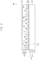
- FIG. 1 is an exploded perspective view illustrating a display device according to an embodiment of the inventive concept.
- FIG. 2 is a cross-sectional view illustrating a backlight unit in FIG. 1 .
- FIG. 3 is a cross-sectional view illustrating a light emission from the backlight unit in FIG. 2 .
- FIG. 4 is a plan view illustrating a reflective pattern layer in FIG. 2 .
- FIG. 5 is an exploded perspective view illustrating a display device according to an embodiment of the inventive concept.
- FIG. 6 is a cross-sectional view illustrating a backlight unit in FIG. 5 .
- FIG. 7 is a cross-sectional view illustrating a light emission from the backlight unit in FIG. 6 .
- FIGS. 1, 2, 3, and 4 a display device according to an embodiment of the inventive concept will be described with reference to FIGS. 1, 2, 3, and 4 .
- FIG. 1 is an exploded perspective view illustrating a display device according to an embodiment of the inventive concept.
- a display device may include a display panel 100 and a backlight unit 200 .
- the display panel 100 may display an image.
- the display panel 100 may be, for example, a liquid crystal display (LCD) panel.
- LCD liquid crystal display
- the display panel 100 may include a first substrate 110 and a second substrate 120 .
- the first substrate 110 may include a plurality of pixels that display images by using light provided from the backlight unit 200 .
- the second substrate 120 is disposed on the first substrate 110 , and the second substrate 120 may face the first substrate 110 .
- the display panel 100 may include a liquid crystal layer (not illustrated) interposed between the first substrate 110 and the second substrate 120 .
- the backlight unit 200 may be located under the display panel 100 .
- the backlight unit 200 may provide light to the display panel 100 .
- the backlight unit 200 may include a light source 210 , a light guide plate 220 , a light conversion layer 230 , a reflective pattern layer 240 , and first barrier layer 251 and second barrier layer 252 .
- FIG. 2 is a cross-sectional view illustrating the backlight unit shown in FIG. 1 .
- the light source 210 may be located at a side of the light guide plate 220 .
- the light source has approximately a same height and width as the light guide plate 220 so as to be aligned with the light guide plate 220 .
- a person of ordinary skill in the art should understand that embodiments of the inventive concept are not limited to structure shown and described in FIGS. 1 and 2 .
- the light source 210 may generate light, and may supply the light to the light guide plate 220 .
- the light source 210 may generate light having a predetermined wavelength.
- the light source 210 may generate light having a wavelength corresponding to blue light.
- the predetermined wavelength of light is not limited to blue, and the light source 210 may be capable of generating light of more than one predetermined wavelength.
- the light source 210 may include a circuit board 211 and a plurality of light emitting elements 212 .
- the circuit board 211 may extend along the side of the light guide plate 220 .
- the light emitting elements 212 may be disposed on the circuit board 211 .
- the light emitting elements 212 may be disposed in a lengthwise direction of the circuit board 211 with a uniform distance in between.
- the light emitting elements 212 may face the side of the light guide plate 220 and may travel through the light guide plate 220 .
- the light emitting elements 212 may generate light having a predetermined wavelength.
- the light emitting elements 212 may generate light having a wavelength corresponding to blue light.
- each of the light emitting elements 212 may be a blue light emitting diode (LED).
- the light guide plate 220 may guide light that is emitted from the light source 210 .
- the light guide plate 220 may guide light provided from the light source 210 to an upper direction. At least some of the light guided to an upper direction may pass through holes 245 in the reflective pattern layer 240 (as shown in FIG. 2 ).
- the light conversion layer 230 may be disposed on the light guide plate 220 . Specifically, the light conversion layer 230 may be located between the light guide plate 220 and the display panel 100 . In other words, the light conversion layer 230 may be located over the light guide plate 220 . There may also be other layers between the light conversion layer 230 and the light guide plate.
- Incident light may be transmitted from the light guide plate 220 to the light conversion layer 230 .
- the incident light may be light Which is generated by the light source 210 and then guided by the light guide plate 220 to the light conversion layer 230 .
- the light conversion layer 230 may convert the incident light into converted light.
- the light conversion layer 230 may convert a wavelength of the incident light.
- the light conversion layer 230 may convert the incident light having a predetermined wavelength into the converted light having a wavelength different from the predetermined wavelength.
- the light conversion layer 230 may convert the incident light having a wavelength corresponding to blue light into the converted light having a wavelength corresponding to red light or green light.
- wavelengths anywhere on the visible spectrum are within the embodiments of the inventive concept.
- the light conversion layer 230 may include a resin 235 , and a plurality of first quantum dots 231 and a plurality of second quantum dots 232 which are accommodated inside the resin 235 .
- the resin 235 may absorb oxygen and moisture from the outside.
- the first quantum dots 231 may generate the converted light by absorbing the incident light.
- quantum dots e.g., nanocrystal phosphors
- the first quantum dots 231 may generate the converted light having a wavelength different from the wavelength of the incident light.
- the first quantum dots 231 may absorb the incident light having a wavelength corresponding to blue light, and may generate the converted light having a wavelength corresponding to red light.
- quantum dots may emit light of specific frequencies based on at least one of the dots' size, shape or material.
- the first quantum dots 231 may be a different shape, size, or made from a different material than the second quantum dots 232 , and each will respectively emit light of a certain frequency based on light (or electricity) being applied.
- the second quantum dots 232 may generate the converted light by absorbing the incident light.
- the second quantum dots 232 may generate the converted light having a wavelength different from the wavelength of the incident light.
- the second quantum dots 232 may absorb the incident light having a wavelength corresponding to blue light, and may generate the converted light having a wavelength corresponding to green light.
- quantum dots designed to generate converted light having a wavelength corresponding to respectfully different colors the various color outputs may be achieved.
- the reflective pattern layer 240 may be disposed between the light guide plate 220 and the light conversion layer 230 .
- light emitted from the light source 210 may be reflected by the reflective pattern layer 240 at angle, such as shown in FIG. 3 .
- light emitted from the light source 210 and then guided by the light guide plate 220 may move forward inside the light guide plate 220 by being reflected by a surface (e.g., a lower surface) of the reflective pattern layer 240 .
- the reflective pattern layer 240 may include metal.
- the reflective pattern layer 240 may include aluminum (Al).
- a material of the reflective pattern layer 240 is not limited thereto, and the reflective pattern layer 240 may include a material that may reflect light, such as metal other than aluminum, a nitride thereof, a mixture thereof, etc.
- the reflective pattern layer may be a nonmetal reflective material.
- a reflective coating can be used. Also it is possible to use a uniformity tape in a light guide plate.
- the reflective pattern layer 240 may include a plurality of holes 245 , such as shown in FIGS. 2, 3 and 4 .
- FIG. 3 shows that light guided by the light guide plate 220 may pass through the holes 245 of the reflective pattern layer 240 .
- light moving forward inside the light guide plate 220 by being reflected by the surface (e.g., the lower surface) of the reflective pattern layer 240 may pass through the holes 245 of the reflective pattern layer 240 , and then may be provided to the light conversion layer 230 .
- FIG. 3 is a cross-sectional view illustrating a light emission from the backlight unit in FIG. 2 .
- a first light L 1 emitted from the light source 210 may move forward inside the light guide plate 220 , and may be converted into a second light L 2 at the light conversion layer 230 .
- the second light L 2 may be provided to the display panel 100 located over the backlight unit 200 .
- the first light L 1 may have a first wavelength, and the first wavelength may be a wavelength corresponding to, for example, blue light.
- the first light L 1 emitted from the light source 210 may be guided by the light guide plate 220 , and may be provided to the light conversion layer 230 by passing through the hole 245 of the reflective pattern layer 240 .
- the first light L 1 incident into the light conversion layer 230 may be absorbed in the first quantum dot 231 , and the first quantum dot 231 may convert the first light L 1 into the second light L 2 .
- IT should also be understood and appreciated by a person of ordinary skill in the art that with reference to FIG.
- the light reflects off lower surface of the light guide plate 220 and then off the reflective pattern layer 240 , there may be some scattering and only a portion of the light may enter a particular hole 245 to be subsequently absorbed by the first quantum dot 231 or the second quantum dot 232 .
- the second light L 2 may have a second wavelength different from the first wavelength, and the second wavelength may be a wavelength corresponding to red light.
- the second light L 2 may move forward in an upper direction of the light conversion layer 230 , and may be provided to the display panel 100 .
- FIG. 3 illustrates that the first light L 1 is absorbed in the first quantum dot 231 .
- the present embodiment of the inventive concept is not limited thereto, and the first light L 1 may be absorbed in the second quantum dot 232 .
- the second light L 2 may have a wavelength corresponding to green light.
- a person of ordinary skill in the art should also understand and appreciate there can be third quantum dots (not shown), etc.
- FIG. 4 is a plan view illustrating a reflective pattern layer in FIG. 2 .
- the holes 245 of the reflective pattern layer 240 may be arranged as a matrix form in a plan view.
- the holes 245 may be disposed in a row direction and/or a column direction with a uniform distance in between.
- a light guide plate may include scattering patterns, and a low refractive layer may be disposed on the light guide plate.
- a low refractive layer is used in the art, for example, to reduce glare from an external source without causing significant deterioration of an image being displayed.
- Light may move forward inside the light guide plate via the low refractive layer, and the light may be provided to a display panel by the scattering patterns.
- a material forming the low refractive layer disposed on the light guide plate may be relatively expensive, and an additional lamination process, etc. may be used to form the scattering patterns inside the light guide plate.
- the backlight unit 200 may include the reflective pattern layer 240 instead of the conventional low refractive layer, and the conventional scattering patterns may not be utilized. Accordingly, a manufacturing cost and a manufacturing time of the backlight unit 200 may be reduced.
- the backlight unit does not include a low refractive layer, yet provides functionality equal or better than backlight units having the low refractive layer, and does so at a reduced cost of manufacture.
- a “low refractive layer” a layer having a low refractive index.
- a low refractive index may be a range of about 1.2 to 1.3.
- the first barrier layer 251 and the second barrier layer 252 may be disposed on the light conversion layer 230 . As shown in FIG. 2 , the light conversion layer 230 is sandwiched between the first barrier layer 251 and the second barrier layer 252 .
- the first barrier layer 251 may be disposed between the light conversion layer 230 and the reflective pattern layer 240
- the second barrier layer 252 may be disposed between the light conversion layer 230 and the display panel 100 .
- the first barrier layer 251 and the second barrier layer 252 may prevent oxygen and moisture from permeating into the light conversion layer 230 , and may protect the first quantum dots 231 and the second quantum dots 232 of the light conversion layer 230 .
- the first barrier layer 251 and the second barrier layer 252 may include an inorganic material.
- the first barrier layer 251 and the second harrier layer 252 may include silicon oxide (SiO x ).
- materials of the first barrier layer 251 and the second barrier layer 252 are not limited thereto, and the first barrier layer 251 and the second barrier layer 252 may include an inorganic material other than silicon oxide and an organic material.
- FIGS. 5, 6, and 7 a display device according to another embodiment of the inventive concept may be described with reference to FIGS. 5, 6, and 7 .
- FIG. 5 is an exploded perspective view illustrating a display device according to an embodiment of the inventive concept.
- a display device may include a display panel 1100 and a backlight unit 1200 .
- the display panel 1100 may display an image.
- the display panel 1100 may be, for example, a liquid crystal display panel.
- the display panel 1100 may include a first substrate 1110 and a second substrate 1120 .
- the first substrate 1110 may include a plurality of pixels that display images by using light provided from the backlight unit 1200 .
- the second substrate 1120 may face the first substrate 1110 .
- the display panel 1100 may include a liquid crystal layer (not illustrated) interposed between the first substrate 1110 and the second substrate 1120 .
- the backlight unit 1200 may be located under the display panel 1100 .
- the backlight unit 1200 may provide light to the display panel 1100 .
- the backlight unit 1200 may include a light source 1210 , a light guide plate 1220 , a light conversion layer 1230 , a reflective pattern layer 1240 , first barrier layer 1251 and second barrier layer 1252 , and a reflective layer 1260 .
- the light guide plate 1220 may have the display panel disposed thereon, and the light guide plate 1220 may be disposed on the reflective pattern layer 1240 and the first barrier layer 1251 , light conversion layer 1230 , and second barrier layer 1252 .
- the arrangement of the light guide plate 1220 and the other layers is different than the embodiment shown in FIG. 1 .
- FIG. 6 is a cross-sectional view illustrating a backlight unit in FIG. 5 .
- the light source 1210 may be located at a side of the light guide plate 1220 .
- the light source 1210 may generate light, and may supply the light to the light guide plate 1220 .
- the light source 1210 may generate light having a predetermined wavelength.
- the light source 1210 may generate light having a wavelength corresponding to blue light.
- the generated light may travel through the light guide plate 1220 , and may reflect off the reflective pattern 1260 .
- the circuit board 1211 may extend along the side of the light guide plate 1220 .
- the light emitting elements 1212 may be disposed on the circuit board 1211 .
- the light emitting elements 1212 may be disposed in a length direction of the circuit board 1211 with a uniform distance in between.
- the light emitting elements 1212 may face the side of the light guide plate 1220 .
- the light emitting elements 1212 may generate light having a predetermined wavelength.
- the light emitting elements 1212 may generate light having a wavelength corresponding to blue light.
- each of the light emitting elements 1212 may be a blue light emitting diode (LED).
- the light guide plate 1220 may guide light emitted from the light source 1210 .
- the light guide plate 1220 may guide the light provided from the light source 1210 to a lower direction.
- the light conversion layer 1230 may be disposed on the light guide plate 1220 .
- the light guide plate 1220 may be located between the light conversion layer 1230 and the display panel 1100 .
- the light conversion layer 1230 may be located under the light guide plate 1220 .
- the light conversion layer 230 is located over the light guide plate 220 .
- Incident light may be transmitted from the light guide plate 1220 to the light conversion layer 1230 .
- the incident light may be light which is generated by the light source 1210 and then guided by the light guide plate 1220 .
- the light conversion layer 1230 may convert the incident light into converted light.
- the light conversion layer 1230 may convert a wavelength of the incident light.
- the light conversion layer 1230 may convert the incident light having a predetermined wavelength into the converted light having a wavelength different from the predetermined wavelength.
- the light conversion layer 1230 may convert the incident light having a wavelength corresponding to blue light into the converted light having a wavelength corresponding to red light or green light. This conversion may be performed through the arrangement of quantum dots sized for conversion to various colors of light.
- the light conversion layer 1230 may include resin 1235 , and a plurality of first quantum dots 1231 and a plurality of second quantum dots 1232 which are accommodated inside the resin 1235 .
- the first quantum dots 1231 and the second quantum dots may convert absorbed incident light into a predetermined color.
- the resin 1235 may absorb oxygen and moisture from the outside.
- the first quantum dots 1231 may generate the converted light by absorbing the incident light.
- the first quantum dots 1231 may generate the converted light having a wavelength different from the wavelength of the incident light.
- the first quantum dots 1231 may absorb the incident light having a wavelength corresponding to blue light, and may generate the converted light having a wavelength corresponding to red light.
- the second quantum dots 1232 may generate the converted light by absorbing the incident light.
- the second quantum dots 1232 may generate the converted light having a wavelength different from the wavelength of the incident light.
- the second quantum dots 1232 may absorb the incident light having a wavelength corresponding to blue light, and may generate the converted light having a wavelength corresponding to green light.
- the light generated by the light source 1210 can be a predetermined color.
- the reflective pattern layer 1240 may be disposed between the light guide plate 1220 and the light conversion layer 1230 .
- FIG. 6 shows the arrangement of the light guide plate 1220 above the reflective pattern layer 1240 .
- embodiments of the inventive concept are not limited to the arrangement shown in FIG. 6 .
- Light emitted from the light source 1210 may be reflected by the reflective pattern layer 1240 .
- light emitted from the light source 1210 and then guided by the light guide plate 1220 may move forward inside the light guide plate 1220 by being reflected by a surface (e.g., an upper surface) of the reflective pattern layer 1240 .
- the reflective pattern layer 1240 may include metal.
- the reflective pattern layer 1240 may include aluminum (Al).
- a material of the reflective pattern layer 1240 is not limited thereto, and the reflective pattern layer 1240 may include a material that may reflect light such as metal other than aluminum, a nitride thereof, a mixture thereof, etc.
- the reflective pattern may be a reflecting coating, or a reflective tape, and is not limited to a metallic construction.
- the reflective pattern layer 1240 may include a plurality of holes 1245 .
- Light guided by the light guide plate 1220 may pass through the holes 1245 of the reflective pattern layer 1240 .
- light moves forward inside the light guide plate 1220 by being reflected off a surface of the light guide and reflected off the surface (e.g., the upper surface) of the reflective pattern layer 1240 .
- the light may pass through the holes 1245 of the reflective pattern layer 1240 , and then may be provided to the light conversion layer 1230 .
- the holes 1245 of the reflective pattern layer 1240 may be arranged as a matrix form in a plan view.
- the holes 1245 may be disposed in a row direction and/or a column direction with a uniform distance in between. While FIG. 4 shows a non-limiting example of an arrangement of a matrix, the holes 1245 in the reflective pattern layer 1240 may be arranged differently than shown.
- the reflective layer 1260 may be disposed under the light conversion layer 1230 .
- the light conversion layer 1230 containing at least the first quantum dots 1231 and the second quantum dots 1232 within resin 1235 may be located between the reflective pattern layer 1240 and the reflective layer 1260 .
- the reflective layer 1260 may reflect the converted light. Specifically, the converted light generated from the light conversion layer 1230 may be reflected by the reflective layer 1260 , and then, may be provided to the display panel 1100 by passing through the holes 1245 of the reflective pattern layer 1240 .
- the reflective layer 1260 may include metal.
- the reflective layer 1260 may include aluminum (Al).
- a material of the reflective layer 1260 is not limited thereto, and the reflective layer 1260 may include a material that may reflect light such as metal other than aluminum, a nitride thereof, a mixture thereof, etc.
- the reflective layer 1260 may also comprise a reflective non-metal coating, or a reflective tape, etc.
- FIG. 7 is a cross-sectional view illustrating a light emission from the backlight unit in FIG. 6 .
- a first light L 1 emitted from the light source 1210 that may move forward inside the light guide plate 1220 , for example by reflection off a surface of the light guide plate and alternately by a reflection off of a surface of the reflective pattern layer 1240 .
- the first light L 1 may pass through one of the holes 1245 and becomes incident on a first quantum dot 1231 or a second quantum dot 1231 .
- the light may be converted into a second light L 2 at the light conversion layer 1230 .
- the second light L 2 may be reflected by the reflective layer 1260 , and may be provided to the display panel 1100 located over the backlight unit 1200 .
- the second light L 2 may be a different color than the first light L 1 .
- the first light L 1 may have a first wavelength, and the first wavelength may be a wavelength corresponding to blue light.
- the first light L 1 emitted from the light source 1210 may be guided by the light guide plate 1220 , and may be provided to the light conversion layer 1230 by passing through the hole 1245 of the reflective pattern layer 1240 .
- the first light L 1 that is incident into the light conversion layer 1230 may be absorbed in the first quantum dot 1231 , and the first quantum dot 1231 may convert the first light L 1 into the second light L 2 .
- the second light L 2 may have a second wavelength different from the first wavelength, and the second wavelength may be a wavelength corresponding to red light.
- the second light L 2 may move forward in a lower direction of the light conversion layer 1230 , and may be reflected by the reflective layer 1260 .
- the second light L 2 reflected by the reflective layer 1260 may move forward in an upper direction of the light conversion layer 1230 , and may be provided to the display panel 1100 .
- FIG. 7 illustrates that the first light L 1 is absorbed in the first quantum dot 1231 .
- the present embodiment is not limited thereto, and the first light L 1 may be absorbed in the second quantum dot 1232 .
- the second light L 2 may have a wavelength corresponding to green light.
- a light guide plate may include scattering patterns, and a low refractive layer may be disposed on the light guide plate.
- Light may move forward (e.g., from a first end of the light guide plate toward a second end of the light guide plate) inside the light guide plate by the low refractive layer, and the light may be provided to a display panel by the scattering patterns.
- a material forming the low refractive layer disposed on the light guide plate is relatively expensive, and the use of a low refractive layer is accompanied by an additional lamination process, etc. may be used to form the scattering patterns inside the light guide plate.
- the backlight unit 1200 may include the reflective pattern layer 1240 instead of the conventional low refractive layer, and the conventional scattering patterns may not be utilized. Accordingly, a manufacturing cost and a manufacturing time of the backlight unit 1200 may be reduced.
- the first barrier layer 1251 and the second barrier layer 1252 may be disposed on the light conversion layer 1230 .
- the first barrier layer 1251 may be disposed between the light conversion layer 1230 and the reflective pattern layer 1240
- the second barrier layer 1252 may be disposed between the light conversion layer 1230 and the reflective layer 1260 .
- the first barrier layer 1251 and the second barrier layer 1252 may prevent oxygen and moisture from permeating into the light conversion layer 1230 , and may protect the first quantum dots 1231 and the second quantum dots 1232 of the light conversion layer 1230 .
- the first barrier layer 1251 and the second barrier layer 1252 may include an inorganic material.
- the first barrier layer 1251 and the second barrier layer 1252 may include silicon oxide (SiO x ).
- materials of the first barrier layer 1251 and the second barrier layer 1252 are not limited thereto, and the first barrier layer 1251 and the second barrier layer 1252 may include an inorganic material other than silicon oxide and an organic material.
- the inorganic material may be a desiccant.
- the backlight unit 1200 may additionally include a sealing member 1270 covering a side portion of the light conversion layer 1230 .
- the sealing member 1270 may cover a side portion of the light conversion layer 1230 , a side portion of the reflective pattern layer 1240 , and a side portion of the first barrier layer 1251 and the second barrier layer 1252 .
- the sealing member 1270 may prevent oxygen and moisture from permeating into the light conversion layer 1230 , and may protect the first quantum dots 1231 and the second quantum dots 1232 of the light conversion layer 1230 .
- the sealing member 1270 may include an inorganic material.
- the sealing member 1270 may include frit.
- a material of the sealing member 1270 is not limited thereto, and the sealing member 1270 may include an organic material.
- the backlight unit according to the embodiments of the inventive concept may be applied to a display device included in a computer, a notebook, a mobile phone, a smartphone, a smart pad, a PMP, a PDA, an MP3 player, or the like, just to name a few non-limiting examples.
Landscapes
- Physics & Mathematics (AREA)
- General Physics & Mathematics (AREA)
- Optics & Photonics (AREA)
- Nonlinear Science (AREA)
- Mathematical Physics (AREA)
- Chemical & Material Sciences (AREA)
- Crystallography & Structural Chemistry (AREA)
- Engineering & Computer Science (AREA)
- Microelectronics & Electronic Packaging (AREA)
- Planar Illumination Modules (AREA)
Abstract
Description
Claims (16)
Applications Claiming Priority (2)
| Application Number | Priority Date | Filing Date | Title |
|---|---|---|---|
| KR10-2018-0002328 | 2018-01-08 | ||
| KR1020180002328A KR102485577B1 (en) | 2018-01-08 | 2018-01-08 | Backlight unit and display device including the same |
Publications (2)
| Publication Number | Publication Date |
|---|---|
| US20190212486A1 US20190212486A1 (en) | 2019-07-11 |
| US10705278B2 true US10705278B2 (en) | 2020-07-07 |
Family
ID=67139482
Family Applications (1)
| Application Number | Title | Priority Date | Filing Date |
|---|---|---|---|
| US16/181,468 Expired - Fee Related US10705278B2 (en) | 2018-01-08 | 2018-11-06 | Backlight unit and display device including the same |
Country Status (3)
| Country | Link |
|---|---|
| US (1) | US10705278B2 (en) |
| KR (1) | KR102485577B1 (en) |
| CN (1) | CN110018592A (en) |
Families Citing this family (5)
| Publication number | Priority date | Publication date | Assignee | Title |
|---|---|---|---|---|
| US10955969B2 (en) * | 2018-08-21 | 2021-03-23 | Pixart Imaging Inc. | Access control system and light guide assembly thereof |
| KR102670429B1 (en) * | 2019-07-25 | 2024-05-29 | 삼성디스플레이 주식회사 | Backlight unit and Display device having the same |
| US11567362B2 (en) * | 2019-08-02 | 2023-01-31 | Beijing Boe Optoelectronics Technology Co., Ltd. | Light guide assembly, light source module and display device |
| KR102694575B1 (en) * | 2019-11-20 | 2024-08-12 | 삼성전자주식회사 | backlight unit and display apparatus comprising thereof |
| CN111474767B (en) * | 2020-04-17 | 2023-05-12 | 京东方科技集团股份有限公司 | Backlight module structure, display panel and display device |
Citations (7)
| Publication number | Priority date | Publication date | Assignee | Title |
|---|---|---|---|---|
| US20120113672A1 (en) * | 2008-12-30 | 2012-05-10 | Nanosys, Inc. | Quantum dot films, lighting devices, and lighting methods |
| US20140022819A1 (en) * | 2011-04-05 | 2014-01-23 | Lg Innotek Co., Ltd. | Optical member and display device including the same |
| US20140063846A1 (en) * | 2012-05-31 | 2014-03-06 | Beijing Boe Display Technology Co., Ltd | Surface light source device and edge-lit type backlight module |
| US20170159910A1 (en) * | 2015-12-07 | 2017-06-08 | Lg Chem, Ltd. | Color conversion film and method for preparing the same |
| US20170322436A1 (en) * | 2015-02-06 | 2017-11-09 | Fujifilm Corporation | Polymerizable composition, wavelength conversion member, backlight unit, and liquid crystal display device |
| US20180299610A1 (en) * | 2015-12-25 | 2018-10-18 | Fujifilm Corporation | Edge light type backlight unit |
| US20190065816A1 (en) * | 2017-08-31 | 2019-02-28 | JENETRIC GmbH | Device for the contact-based simultaneous capture of prints of autopodia |
Family Cites Families (5)
| Publication number | Priority date | Publication date | Assignee | Title |
|---|---|---|---|---|
| KR20110057518A (en) * | 2009-11-24 | 2011-06-01 | 엘지디스플레이 주식회사 | Reflective light guide, backlight unit and liquid crystal display using the same |
| KR101484480B1 (en) | 2014-06-20 | 2015-01-20 | 문승호 | Direct Type surface light source device |
| KR101686737B1 (en) * | 2015-04-30 | 2016-12-14 | 엘지전자 주식회사 | Light conversion plate, light emitting diode package, backlight unit and display device comprising the same |
| CN205015587U (en) * | 2015-09-16 | 2016-02-03 | 深圳Tcl新技术有限公司 | Backlight module group and liquid crystal display |
| CN105867019A (en) * | 2016-03-30 | 2016-08-17 | 苏州星烁纳米科技有限公司 | Wavelength conversion element, backlight module and display device |
-
2018
- 2018-01-08 KR KR1020180002328A patent/KR102485577B1/en active Active
- 2018-11-06 US US16/181,468 patent/US10705278B2/en not_active Expired - Fee Related
-
2019
- 2019-01-07 CN CN201910011403.9A patent/CN110018592A/en active Pending
Patent Citations (7)
| Publication number | Priority date | Publication date | Assignee | Title |
|---|---|---|---|---|
| US20120113672A1 (en) * | 2008-12-30 | 2012-05-10 | Nanosys, Inc. | Quantum dot films, lighting devices, and lighting methods |
| US20140022819A1 (en) * | 2011-04-05 | 2014-01-23 | Lg Innotek Co., Ltd. | Optical member and display device including the same |
| US20140063846A1 (en) * | 2012-05-31 | 2014-03-06 | Beijing Boe Display Technology Co., Ltd | Surface light source device and edge-lit type backlight module |
| US20170322436A1 (en) * | 2015-02-06 | 2017-11-09 | Fujifilm Corporation | Polymerizable composition, wavelength conversion member, backlight unit, and liquid crystal display device |
| US20170159910A1 (en) * | 2015-12-07 | 2017-06-08 | Lg Chem, Ltd. | Color conversion film and method for preparing the same |
| US20180299610A1 (en) * | 2015-12-25 | 2018-10-18 | Fujifilm Corporation | Edge light type backlight unit |
| US20190065816A1 (en) * | 2017-08-31 | 2019-02-28 | JENETRIC GmbH | Device for the contact-based simultaneous capture of prints of autopodia |
Also Published As
| Publication number | Publication date |
|---|---|
| CN110018592A (en) | 2019-07-16 |
| US20190212486A1 (en) | 2019-07-11 |
| KR102485577B1 (en) | 2023-01-09 |
| KR20190085195A (en) | 2019-07-18 |
Similar Documents
| Publication | Publication Date | Title |
|---|---|---|
| US10705278B2 (en) | Backlight unit and display device including the same | |
| KR102599014B1 (en) | Color conversion assembly and its manufacturing method and display panel | |
| KR102090163B1 (en) | Back-light unit and display apparatus having the same | |
| US9625639B2 (en) | Optical member and display device including the same | |
| US9459395B2 (en) | Backlight assembly and liquid crystal display including the same | |
| KR101970552B1 (en) | Diffusion sheet having quantum dot and backlight unit inculding the same | |
| TWI472842B (en) | Display device and back light module thereof | |
| US20130002986A1 (en) | Display device | |
| US10310324B2 (en) | Backlight module | |
| TW201624688A (en) | Display panel | |
| WO2011142170A1 (en) | Illumination device, display device, television receiving device | |
| US10763401B2 (en) | Backlight unit and display apparatus including the same | |
| CN110133906A (en) | Lighting device, display device and radiovisor | |
| KR20150033437A (en) | Backlight assembly, display apparatus having the same and method of manufacturing the same | |
| CN108828834A (en) | Display panel | |
| KR20170000444A (en) | Liquid crystal display apparatus | |
| US20250020956A1 (en) | Spliced display device | |
| JP2019139906A (en) | Illumination device, display device, and television receiver | |
| KR102298922B1 (en) | Liquid crystal display device | |
| US11353740B2 (en) | Backlight unit and display device using the same | |
| US10330265B2 (en) | Front light source and display device comprising the front light source | |
| KR20110022970A (en) | Display | |
| JP2017117531A (en) | Luminaire and display device | |
| KR102416031B1 (en) | Backlight unit and display device including the same | |
| KR101513157B1 (en) | Backlight and liquid crystal display device having the same |
Legal Events
| Date | Code | Title | Description |
|---|---|---|---|
| AS | Assignment |
Owner name: SAMSUNG DISPLAY CO., LTD., KOREA, REPUBLIC OF Free format text: ASSIGNMENT OF ASSIGNORS INTEREST;ASSIGNORS:AHN, JEAHEON;MAENG, CHEONJAE;SON, DONGIL;AND OTHERS;SIGNING DATES FROM 20180607 TO 20180616;REEL/FRAME:047418/0130 |
|
| FEPP | Fee payment procedure |
Free format text: ENTITY STATUS SET TO UNDISCOUNTED (ORIGINAL EVENT CODE: BIG.); ENTITY STATUS OF PATENT OWNER: LARGE ENTITY |
|
| STPP | Information on status: patent application and granting procedure in general |
Free format text: NON FINAL ACTION MAILED |
|
| STPP | Information on status: patent application and granting procedure in general |
Free format text: RESPONSE TO NON-FINAL OFFICE ACTION ENTERED AND FORWARDED TO EXAMINER |
|
| STPP | Information on status: patent application and granting procedure in general |
Free format text: NOTICE OF ALLOWANCE MAILED -- APPLICATION RECEIVED IN OFFICE OF PUBLICATIONS |
|
| STPP | Information on status: patent application and granting procedure in general |
Free format text: PUBLICATIONS -- ISSUE FEE PAYMENT VERIFIED |
|
| STCF | Information on status: patent grant |
Free format text: PATENTED CASE |
|
| FEPP | Fee payment procedure |
Free format text: MAINTENANCE FEE REMINDER MAILED (ORIGINAL EVENT CODE: REM.); ENTITY STATUS OF PATENT OWNER: LARGE ENTITY |
|
| LAPS | Lapse for failure to pay maintenance fees |
Free format text: PATENT EXPIRED FOR FAILURE TO PAY MAINTENANCE FEES (ORIGINAL EVENT CODE: EXP.); ENTITY STATUS OF PATENT OWNER: LARGE ENTITY |
|
| STCH | Information on status: patent discontinuation |
Free format text: PATENT EXPIRED DUE TO NONPAYMENT OF MAINTENANCE FEES UNDER 37 CFR 1.362 |
|
| FP | Lapsed due to failure to pay maintenance fee |
Effective date: 20240707 |