US10692952B2 - OLED substrate and display device - Google Patents

OLED substrate and display device Download PDF

Info

Publication number
US10692952B2
US10692952B2 US16/446,067 US201916446067A US10692952B2 US 10692952 B2 US10692952 B2 US 10692952B2 US 201916446067 A US201916446067 A US 201916446067A US 10692952 B2 US10692952 B2 US 10692952B2
Authority
US
United States
Prior art keywords
light
layer
shielding layer
oled substrate
thin
Prior art date
Legal status (The legal status is an assumption and is not a legal conclusion. Google has not performed a legal analysis and makes no representation as to the accuracy of the status listed.)
Active
Application number
US16/446,067
Other versions
US20200020757A1 (en
Inventor
Haixu Li
Zhanfeng CAO
Current Assignee (The listed assignees may be inaccurate. Google has not performed a legal analysis and makes no representation or warranty as to the accuracy of the list.)
BOE Technology Group Co Ltd
Original Assignee
BOE Technology Group Co Ltd
Priority date (The priority date is an assumption and is not a legal conclusion. Google has not performed a legal analysis and makes no representation as to the accuracy of the date listed.)
Filing date
Publication date
Application filed by BOE Technology Group Co Ltd filed Critical BOE Technology Group Co Ltd
Assigned to BOE TECHNOLOGY GROUP CO., LTD. reassignment BOE TECHNOLOGY GROUP CO., LTD. ASSIGNMENT OF ASSIGNORS INTEREST (SEE DOCUMENT FOR DETAILS). Assignors: CAO, ZHANFENG, LI, HAIXU
Publication of US20200020757A1 publication Critical patent/US20200020757A1/en
Application granted granted Critical
Publication of US10692952B2 publication Critical patent/US10692952B2/en
Active legal-status Critical Current
Anticipated expiration legal-status Critical

Links

Images

Classifications

    • H01L27/3272
    • HELECTRICITY
    • H10SEMICONDUCTOR DEVICES; ELECTRIC SOLID-STATE DEVICES NOT OTHERWISE PROVIDED FOR
    • H10KORGANIC ELECTRIC SOLID-STATE DEVICES
    • H10K59/00Integrated devices, or assemblies of multiple devices, comprising at least one organic light-emitting element covered by group H10K50/00
    • H10K59/10OLED displays
    • H10K59/12Active-matrix OLED [AMOLED] displays
    • H10K59/124Insulating layers formed between TFT elements and OLED elements
    • H01L27/3258
    • H01L51/5281
    • HELECTRICITY
    • H10SEMICONDUCTOR DEVICES; ELECTRIC SOLID-STATE DEVICES NOT OTHERWISE PROVIDED FOR
    • H10KORGANIC ELECTRIC SOLID-STATE DEVICES
    • H10K50/00Organic light-emitting devices
    • H10K50/80Constructional details
    • H10K50/86Arrangements for improving contrast, e.g. preventing reflection of ambient light
    • HELECTRICITY
    • H10SEMICONDUCTOR DEVICES; ELECTRIC SOLID-STATE DEVICES NOT OTHERWISE PROVIDED FOR
    • H10KORGANIC ELECTRIC SOLID-STATE DEVICES
    • H10K59/00Integrated devices, or assemblies of multiple devices, comprising at least one organic light-emitting element covered by group H10K50/00
    • H10K59/10OLED displays
    • H10K59/12Active-matrix OLED [AMOLED] displays
    • H10K59/126Shielding, e.g. light-blocking means over the TFTs
    • HELECTRICITY
    • H10SEMICONDUCTOR DEVICES; ELECTRIC SOLID-STATE DEVICES NOT OTHERWISE PROVIDED FOR
    • H10KORGANIC ELECTRIC SOLID-STATE DEVICES
    • H10K59/00Integrated devices, or assemblies of multiple devices, comprising at least one organic light-emitting element covered by group H10K50/00
    • H10K59/80Constructional details
    • H10K59/8791Arrangements for improving contrast, e.g. preventing reflection of ambient light
    • H10K59/8792Arrangements for improving contrast, e.g. preventing reflection of ambient light comprising light absorbing layers, e.g. black layers
    • HELECTRICITY
    • H10SEMICONDUCTOR DEVICES; ELECTRIC SOLID-STATE DEVICES NOT OTHERWISE PROVIDED FOR
    • H10KORGANIC ELECTRIC SOLID-STATE DEVICES
    • H10K59/00Integrated devices, or assemblies of multiple devices, comprising at least one organic light-emitting element covered by group H10K50/00
    • H10K59/80Constructional details
    • H10K59/87Passivation; Containers; Encapsulations

Definitions

  • the present disclosure relates to the field of display technology, and in particular to an OLED substrate and a display device.
  • Organic electro-luminescent display has been widely used in the fields of display, illumination and others, due to its self-illumination, low operating voltage, light weight, flexibility, and high color saturation etc.
  • the preparation process of the organic electro-luminescent device includes: forming a thin-film transistor (TFT) on the substrate, and forming an anode, a pixel defining layer, a light-emitting layer and a cathode in sequence on the thin-film transistor, in which the anode and the thin-film transistor are electrically connected to the drain electrode.
  • TFT thin-film transistor
  • the portion of the light emitted from the light-emitting layer is incident on the active layer of the thin-film transistor through the refraction and reflection of the film layer in the organic electro-luminescent device, the portion of the light affects the characteristics of the thin-film transistor. This causes an instability of the threshold voltage (V th ) of the thin-film transistor and an increase in off-state current (I off ), thereby affecting the light-emitting effect.
  • V th threshold voltage
  • I off off-state current
  • LTPS low temperature poly-silicon
  • the present disclosure provides an OLED substrate including a base substrate, and a thin-film transistor, a first electrode, and a light-emitting layer arranged in sequence on the base substrate, in which the OLED substrate further includes a light-shielding layer arranged between an active layer and the first electrode.
  • a material of which the light-shielding layer is made includes amorphous silicon
  • the OLED substrate further includes side layers arranged on two opposite sides of the light-shielding layer and in contact with the light-shielding layer, and a material of which the side layers are made is an insulating material.
  • the material of the light-shielding layer further includes sulfur doped in the amorphous silicon.
  • the sulfur has a mass ratio of 0.5% to 5% based on the total mass of the material of the light-shielding layer.
  • the light-shielding layer includes a plurality of depression portions on a side proximate to the light-emitting layer.
  • a cross-sectional shape of the depression portion obtained by cutting the light-shielding layer along a thickness direction of the OLED substrate is a triangle.
  • the depression portion does not penetrate the light-shielding layer.
  • the thin-film transistor further includes an insulating layer arranged on a side of the active layer proximate to the light-emitting layer
  • the OLED substrate further includes a planarization layer between the thin-film transistor and the first electrode, and the insulating layer or the planarization is also used as the light-shielding layer.
  • the thin-film transistor further includes an insulating layer arranged on a side of the active layer proximate to the light-emitting layer
  • the OLED substrate further includes a planarization layer between the thin-film transistor and the first electrode, and the side layers and the insulating layer are also used as the light-shielding layer as a whole, or the planarization layer is also used as the light-shielding layer.
  • the present disclosure provides a display device including any of the above OLED substrates.
  • FIG. 1 is a schematic view of an OLED substrate according to an embodiment of the present disclosure.
  • FIG. 2 is a schematic view of an OLED substrate according to another embodiment of the present disclosure.
  • FIG. 3 is a schematic view of an OLED substrate according to a still another embodiment of the present disclosure.
  • FIG. 4 is a schematic view of an OLED substrate according to a still another embodiment of the present disclosure.
  • FIG. 5( a ) is a schematic view of an OLED substrate according to a still another embodiment of the present disclosure.
  • FIG. 5( b ) is a schematic view of an OLED substrate according to a still another embodiment of the present disclosure.
  • FIG. 6 is a schematic view of forming a lower side layer and a light-shielding layer on a base substrate according to a still another embodiment of the present disclosure.
  • FIG. 7 is a schematic view of forming a lower side layer, a light-shielding layer, and an upper side layer on a base substrate according to a still another embodiment of the present disclosure.
  • FIG. 8 is a schematic view of an optical path reflected and refracted after incident light is incident on a depression portion according to a still another embodiment of the present disclosure.
  • FIG. 9 is a schematic view of forming a source contact hole and a drain contact hole on an interlayer dielectric layer and a gate insulating layer according to a still another embodiment of the present disclosure.
  • the OLED substrate and the display device of the present disclosure can solve the problem that light emitted from the light-emitting layer in the organic electro-luminescent device is incident on the active layer, thereby affecting the characteristics of the thin-film transistor.
  • the present disclosure solves the technical problem by any of the following technical solutions.
  • an OLED substrate including a base substrate, and a thin-film transistor, a first electrode, and a light-emitting layer arranged in sequence on the base substrate, wherein the OLED substrate further includes a light-shielding layer arranged between an active layer of the thin-film transistor and the first electrode.
  • the OLED includes a base substrate 10 , and a thin-film transistor 20 , a first electrode 50 , and a light-emitting layer 30 which are arranged on the base substrate 10 in sequence;
  • the thin-film transistor 20 includes an active layer 201 ;
  • the OLED substrate further includes a light-shielding layer 40 arranged between the active layer 201 and the first electrode 50 .
  • the OLED substrate further includes a light-shielding layer arranged between the active layer and the first electrode
  • the light-shielding layer may block light emitted from the light-emitting layer, to prevent the light emitted by the layer from being incident on the active layer and thus affecting the characteristics of the thin-film transistor. Therefore, the present disclosure stabilizes the light-emitting characteristics of the OLED substrate and increases the light-emitting stability.
  • the light-shielding layer can not only block the ambient light incident on the OLED substrate, but also shield the light emitted from the light-emitting layer. This prevents ambient light from being emitted onto the active layer, thereby preventing from affecting the characteristics of the thin-film transistor.
  • the thin-film transistor 20 includes a gate electrode 203 , a gate insulating layer (GI) 202 , a source electrode 206 , and a drain electrode 205 , in addition to the active layer 201 .
  • the source electrode 206 and the drain electrode 205 are in contact with the active layer 201 through the via hole, and the drain electrode 205 of the thin-film transistor 20 is electrically connected to the first electrode 50 .
  • the thin-film transistor 20 may further include a film layer, such as an interlayer dielectric layer (ILD) 204 .
  • ILD interlayer dielectric layer
  • the type of the thin-film transistor 20 is not limited.
  • the thin-film transistor 20 may be, for example, an amorphous silicon (a-Si) thin-film transistor, a single crystal silicon thin-film transistor, or a low temperature poly-silicon thin-film transistor. Since the low temperature poly-silicon thin-film transistor has advantages of high mobility, reducing response time, reducing power consumption, and increasing resolution and contrast, a low temperature poly-silicon thin-film transistor is often selected as the thin-film transistor 20 in the organic electro-luminescent device. Low temperature poly-silicon is more sensitive to light than amorphous silicon and single crystal silicon. Therefore, the characteristics of the low temperature poly-silicon thin-film transistor are more susceptible to illumination.
  • the OLED substrate includes a pixel definition layer (PDL) 60 arranged between the first electrode 50 and the light-emitting layer 30 and a second electrode 70 arranged on the light-emitting layer 30 , in addition to the thin-film transistor 20 , the first electrode 50 , and the light-emitting layer 30 which are arranged on the base substrate 10 in sequence, as shown in FIG. 1 .
  • the pixel defining layer 60 is divided into an open area and a pixel defining area for defining an open area.
  • the light-emitting layer 30 is located in an open area of the pixel defining layer 60 .
  • the first electrode 50 and the second electrode 70 are used to drive the light-emitting layer 30 to emit light.
  • the first electrode 50 may be an anode
  • the second electrode 70 may be a cathode; or the first electrode 50 may be a cathode, and the second electrode 70 may be an anode.
  • the OLED substrate may further include at least one of an electron transport layer, an electron injection layer, a hole transport layer, and a hole injection layer arranged between the first electrode 50 and the second electrode 70 .
  • the OLED substrate is further provided with a planarization layer (PLN) 80 between the thin-film transistor 20 and the first electrode 50 .
  • PPN planarization layer
  • the preparation process of the OLED substrate may specifically include: firstly forming a thin-film transistor 20 on the substrate 10 , forming a planarization 80 on the thin-film transistor 20 , and then forming the first electrode 50 , the pixel defining layer 60 , and the light-emitting layer 30 and second electrode 70 in sequence.
  • the installation position of the light-shielding layer 40 is not limited, as long as it is arranged between the active layer 201 and the first electrode 50 .
  • the light-shielding layer 40 can be shared with the film layer originally present on the OLED substrate.
  • the light-shielding layer 40 is shared with the interlayer dielectric layer 204 in the thin-film transistor 20 , or the light-shielding layer 40 is shared with the gate insulating layer 202 in the thin-film transistor 20 . That is, the interlayer dielectric layer 204 or the gate insulating layer 202 in the thin-film transistor 20 is also used as the light-shielding layer 40 .
  • the light-shielding layer 40 may be additionally formed, that is, the light-shielding layer 40 is a layer different from the insulating layer such as the interlayer dielectric layer 204 or the gate insulating layer 202 .
  • the light-shielding layer 40 may be a light-absorbing layer.
  • the material for preparing the light-shielding layer 40 may be, for example, a black ink or a black resin.
  • the light-shielding layer 40 may also be a reflective layer.
  • the material for preparing the light-shielding layer 40 may be, for example, a metal material.
  • the reflective layer reflects the light emitted by the light-emitting layer 30 or the ambient light that is incident thereon, and the excessive reflected light affects the light-emitting effect of the OLED substrate. Therefore, the light-shielding layer 40 of the embodiment of the present disclosure is preferably a light-absorbing layer.
  • a buffer layer 90 may be arranged between the base substrate 10 and the thin-film transistor 20 .
  • the buffer layer 90 can not only flatten the base substrate 10 and shield the defects of the substrate 10 , but also prevent impurity ions from penetrating into the base substrate 10 to cause various defects of the device.
  • the material for preparing the light-shielding layer 40 includes amorphous silicon.
  • the OLED substrate further includes side layers 401 arranged on the upper and lower surface sides of the light-shielding layer 40 and in contact with the light-shielding layer 40 .
  • the material for the side layer 401 is an insulating material.
  • Amorphous silicon has a greater absorption to visible light, especially to short-wavelength visible light. Therefore, when the material of the light-shielding layer 40 includes amorphous silicon, the light-shielding layer 40 corresponds to the light-absorbing layer, and visible light can be absorbed.
  • the light-shielding layer 40 provided in the OLED substrate of the embodiment of the present disclosure should not affect the performance of other film layers or devices; when the material of the light-shielding layer 40 includes amorphous silicon of a semiconductor material, in order to avoid the influence of amorphous silicon on the performance of other film layers, such that upper and lower side layers 401 , which are in contact with the light-shielding layer 40 , are arranged on the upper and lower sides of the amorphous silicon layer.
  • the material for preparing the side layer 401 is an insulating material.
  • the material of the side layers 401 may be, for example, at least one of silicon oxide (SiO x ), silicon nitride (SiN x ), or silicon oxynitride (SiO x N y ).
  • the thicknesses of the light-shielding layer 40 and the upper and lower side layers 401 are not limited.
  • the thickness of the light-shielding layer may be 2000 ⁇ to 5000 ⁇ .
  • one of the upper and lower side layers 401 may have a thickness of 1000 ⁇ to 3000 ⁇ .
  • the upper and lower side layers 401 when the upper and lower side layers 401 are made of silicon oxide, one of the upper and lower side layers 401 may have a thickness of 1000 ⁇ to 3000 ⁇ ; and when the upper and lower side layers 401 are made of silicon nitride, the upper and lower side layers 401 have a thickness of 2000 ⁇ to 3000 ⁇ .
  • the light-shielding layer 40 can absorb the light emitted from the light-emitting layer 30 and block the light emitted from the light-emitting layer 30 from being incident on the active layer 201 , thereby preventing form affecting the characteristics of the thin-film transistor.
  • the light-shielding layer 40 can also absorb external ambient light incident into the OLED substrate, thereby preventing the excessive reflected light, after the external ambient light and the light emitted by the light-emitting layer 30 is reflected by the film layer in the OLED substrate, from affecting the light-emitting effect.
  • the material for preparing the light-shielding layer 40 includes amorphous silicon, although amorphous silicon can absorb visible light, amorphous silicon still has a transmittance of about 30% to 70% for long-wavelength visible light (for example, red light and green light).
  • the material for preparing the light-shielding layer 40 further includes sulfur (S) doped in amorphous silicon. It should be noted that after sulfur is doped into a-Si, the light-absorbing performance of the light-shielding layer 40 is increased, and the reason why the addition of sulfur increases the light-absorbing performance is that an impurity state contributed by the dopant atoms appears below the conduction band of the a-Si, so that the band is narrowed.
  • the material for preparing light-shielding layer 40 there is no limitation on how to allow the material for preparing light-shielding layer 40 to contain amorphous silicon and sulfur doped in amorphous silicon.
  • Two specific implementations are provided below as examples.
  • First, the amorphous silicon and the sulfur are first doped and mixed, and then the light-shielding layer 40 is formed.
  • SF 6 sulfur hexafluoride
  • the content of sulfur doped in the amorphous silicon is not limited, and an appropriate amount of sulfur may be doped into the amorphous silicon as needed. If the content of sulfur doped in the amorphous silicon is too small, the improvement in the light-absorbing effect of the light-shielding layer 40 is not obvious.
  • the light-absorbing effect of the light-shielding layer 40 gradually increases as the content of sulfur doped in the amorphous silicon increases. However, when the sulfur content is increased to a certain extent, the light-absorbing effect of the light-shielding layer 40 does not increase. Therefore, the mass of sulfur in the embodiment of the present disclosure is preferably 0.5% to 5% based on the total mass of the material of the light-shielding layer 40 .
  • the material of the light-shielding layer 40 includes amorphous silicon
  • doping sulfur in the amorphous silicon improves the light-absorbing efficiency and the light-absorbing intensity of the light-shielding layer 40 , thereby enhancing the light-shielding effect of the light-shielding layer 40 .
  • the light-shielding layer 40 includes a plurality of depression portions 402 on a side proximate to the light-emitting layer 30 .
  • the cross-sectional shape of the depression portion 402 taken along the thickness direction of the OLED substrate is not limited.
  • the cross-sectional shape of the depression portion 402 may be a triangle as shown in FIGS. 5( a ) and 5( b ) , or a trapezoidal, semi-circular shape (in which a semicircle is not shown in the drawing), or the like.
  • the plurality of depression portions 402 arranged on a side proximate to the light-emitting layer 30 may be distributed in a dot shape on the light-shielding layer 40 or may be distributed in a strip shape on the light-shielding layer 40 .
  • the depression depth of the depression portion 402 is not limited, and may be set as needed.
  • the depression portion 402 may not penetrate the light-shielding layer 40 as shown in FIG. 5( a ) , or may penetrate the light-shielding layer 40 as shown in FIG. 5( b ) .
  • the depression portion 402 does not penetrate the light-shielding layer 40 , the light is incident on the depression portion 402 and passes through the remaining thickness of the light-shielding layer 40 , thereby further ensuring the absorption of light. Therefore, the depression portion 402 of the embodiment of the present disclosure preferably does not penetrate the light-shielding layer 40 .
  • the light-shielding layer 40 includes the first light-shielding sublayer and the second light-shielding sublayer which are laminated.
  • the first light-shielding sublayer is provided with a depression portion 402
  • the thickness of the first light-shielding sublayer is the same as the depression depth of the depression portion 402 .
  • the thickness of the second light-shielding sublayer is not limited. In an optional embodiment of the present disclosure, the second light-shielding sublayer has a thickness of 100 to 900 ⁇ .
  • the formation of the depression portion 402 on the side of the light-shielding layer 40 proximate to the light-emitting layer 30 is not limited.
  • a light-shielding layer film can be formed first.
  • the light-shielding layer film may be formed by a deposition method, and the light-shielding layer film may be exposed, developed, and etched, for example, by a dry etch process, to form the light-shielding layer 40 . That is, a plurality of depression portions 402 is formed on the light-shielding layer film by an incomplete etching method.
  • the lower side layer 401 may be deposited first, a light-shielding layer thin film is further formed, and the light-shielding layer thin film is patterned to form the light-shielding layer 40 , and then the upper side layer 401 is further formed on the light-shielding layer 40 , as shown in FIG. 7 .
  • the light-shielding layer 40 since the light-shielding layer 40 includes a plurality of depression portions 402 on a side proximate to the light-emitting layer 30 , the depression portion 402 facilitates the falling of the incident light and reduces the reflected light, thereby improving the light-absorbing effect of the light-shielding layer 40 .
  • the cross-sectional shape of the depression portion 402 obtained after the light-shielding layer 40 is cut along the thickness direction of the OLED substrate is a triangle, as shown in FIG. 8 , after the incident light is incident on the depression portion 402 , a portion of the light is reflected, and a portion of the light is refracted. The refracted light is absorbed. After the incident light is reflected and refracted multiple times, the intensity of the light finally reflected from the light-shielding layer 40 is greatly weakened, thereby effectively improving the light-absorbing effect of the light-shielding layer 40 . Therefore, as shown in FIGS. 5( a ) and 5( b ) , the cross-sectional shape of the depression portion 402 obtained by taking the light-shielding layer 40 along the thickness direction of the OLED substrate is preferably a triangle.
  • the depression portion 402 When the cross-sectional shape of the depression portion 402 obtained by taking the light-shielding layer 40 along the thickness direction of the OLED substrate is a triangle, the depression portion 402 may be distributed in a dot shape on the light-shielding layer 40 or may be distributed in a strip shape on the light-shielding layer 40 .
  • the depression portions 402 are distributed in a dot shape on the light-shielding layer 40 .
  • the depression portion 402 when the depression portion 402 is distributed in a dot shape on the light-shielding layer 40 , the depression portion 402 has a conical structure.
  • the thin-film transistor 20 further includes an insulating layer arranged on a side of the active layer 201 proximate to the light-emitting layer 30 .
  • the OLED substrate further includes a planarization layer 80 arranged between the thin-film transistor 20 and the first electrode 50 .
  • the light-shielding layer 40 is shared with the insulating layer or the planarization layer 80 , that is, the insulating layer and the planarization are also used as the light-shielding layer.
  • the thin-film transistor 20 in the case where the light-shielding layer 40 is shared with the insulating layer, the thin-film transistor 20 , as shown in FIG. 2 , includes the active layer 201 , the gate insulating layer 202 , the gate electrode 203 , and the interlayer dielectric layer 204 , the source electrode 206 , and the drain electrode 205 , which are arranged in sequence.
  • the insulating layer of the thin-film transistor 20 may be the gate insulating layer 202 or the interlayer dielectric layer 204
  • the light-shielding layer 40 may be shared with the gate insulating layer 202 , or shared with the light-shielding layer 40 and the interlayer dielectric layer 204 as shown in FIGS.
  • the thin-film transistor includes the active layer 201 , the source electrode 206 , the drain electrode 205 , the gate insulating layer 202 , and the gate electrode 203 which are arranged in sequence
  • the insulating layer of the thin-film transistor 20 is the gate insulating layer 202 , and thus the light-shielding layer 40 is shared with the gate insulating layer 202 .
  • the light-shielding layer 40 When the light-shielding layer 40 is shared with the insulating layer, the light-shielding layer 40 should serve both as a function of light-shielding and as a function of insulation. When the light-shielding layer 40 is shared with the planarization layer 80 , the light-shielding layer 40 should serve both as a function of light-shielding and as a function of flattening.
  • the step of separately forming the light-shielding layer can be reduced as compared with additionally providing the light-shielding layer 40 . This simplifies the preparation process of the OLED substrate.
  • the thin-film transistor 20 further includes an insulating layer arranged on a side of the active layer 201 proximate to the light-emitting layer 30 .
  • the OLED substrate further includes a planarization layer 80 arranged between the thin-film transistor 20 and the first electrode 50 .
  • the light-shielding layer 40 and the two side layers 401 are combined with the insulating layer or shared with the planarization layer 80 , that is, the two side layers 401 and the insulating layer are also used integrally as the light-shielding layer 40 , or the planarization layer 80 is also used as the light-shielding layer.
  • the thin-film transistor 20 includes the active layer 201 , the gate insulating layer 202 , the gate electrode 203 , and the interlayer dielectric layer 204 , the source electrode 206 , and the drain electrode 205 , which are arranged in sequence.
  • the insulating layer of the thin-film transistor 20 may be the gate insulating layer 202 or the interlayer dielectric layer 204
  • the light-shielding layer 40 and two side layers 401 may be shared with the gate insulating layer 202 , or shared with the light-shielding layer 40 and two side layers 401 as shown in FIGS. 4, 5 ( a ), 5 ( b ), 7 and 9 .
  • the insulating layer of the thin-film transistor 20 is the gate insulating layer 202 , and thus the light-shielding layer 40 and the two side layers 401 are shared with the gate insulating layer 202 .
  • the process for preparing the thin-film transistor includes: after the forming the gate insulating layer 202 , the gate electrode 203 and the interlayer dielectric layer 204 in sequence, as shown in FIG. 9 (in FIG.
  • the light-shielding layer 40 and the two side layers 401 are shared with the interlayer dielectric layer 204 as an example), a dielectric layer 204 and a gate insulating layer 202 are exposed, developed, and etched to form a source contact via hole and a drain contact via hole, and then a source electrode 206 and a drain electrode 205 are formed.
  • the source electrode 206 is in contact with the active layer 201 through a source contact hole
  • the drain electrode 205 is in contact with the active layer 201 through a drain contact hole.
  • the light-shielding layer 40 and the two upper and lower side layers 401 When the light-shielding layer 40 and the two upper and lower side layers 401 are shared with the insulating layer, the light-shielding layer 40 and the two upper and lower side layers 401 should serve both as a function of light-shielding and as a function of insulation; and when the light-shielding layer 40 and the two upper and lower side layers 401 are shared with the planarization 80 , the light-shielding layer 40 and the two upper and lower side layers 401 should serve both as a function of light-shielding and as a function of flattening.
  • the step of forming one light-shielding layer can be reduced as compared with the additional providing the light-shielding layer 40 . This simplifies the preparation process of the OLED substrate.
  • Another embodiment of the present disclosure further provides a display device including any of the above OLED substrates.
  • the display device may be any device that displays an image regardless of being movable (e.g., video) or fixed (e.g., still image) and regardless of text or picture. More specifically, it is expected that the described embodiments can be implemented in or associated with various electronic devices.
  • the various electronic devices include, but not limited to, mobile phones, wireless devices, personal data assistants (PDA), handheld or portable computers, GPS receivers/navigators, cameras, MP4 video players, video cameras, game consoles, watches, clocks, calculators, television monitors, flat panel displays, computer monitors, car displays (e.g., odometer display, etc.), navigator, cockpit controller and/or displays, camera view displays (e.g., displays for a rear-view camera in a vehicle) electronic photographs, electronic billboards or signs, projectors, architectural structures, packaging and aesthetic structures (e.g., displays for images of a piece of jewelry), etc.
  • the display device may also be a display panel.
  • the display device includes a package film or a package substrate for packaging the OLED substrate, in addition to the OLED substrate.
  • a display device includes the above-described OLED substrate.
  • the OLED substrate in the display device has the same technical features and advantageous effects as the OLED substrate described above. Since the technical features and advantageous effects of the OLED substrate have been described in detail above, they will be not described herein again.

Landscapes

  • Engineering & Computer Science (AREA)
  • Microelectronics & Electronic Packaging (AREA)
  • Physics & Mathematics (AREA)
  • Optics & Photonics (AREA)
  • Electroluminescent Light Sources (AREA)
  • Devices For Indicating Variable Information By Combining Individual Elements (AREA)

Abstract

The present disclosure provides an OLED substrate and a display device. The OLED substrate includes a base substrate, and a thin-film transistor, a first electrode, and a light-emitting layer arranged in sequence on the base substrate, in which the OLED substrate further includes a light-shielding layer arranged between an active layer of the thin-film transistor and the first electrode.

Description

CROSS-REFERENCE TO RELATED APPLICATION
This application claims priority to Chinese Patent Application No. 201810772090.4 filed on Jul. 13, 2018, which is incorporated herein by reference in its entirety.
TECHNICAL FIELD
The present disclosure relates to the field of display technology, and in particular to an OLED substrate and a display device.
BACKGROUND
Organic electro-luminescent display (OLED) has been widely used in the fields of display, illumination and others, due to its self-illumination, low operating voltage, light weight, flexibility, and high color saturation etc. The preparation process of the organic electro-luminescent device includes: forming a thin-film transistor (TFT) on the substrate, and forming an anode, a pixel defining layer, a light-emitting layer and a cathode in sequence on the thin-film transistor, in which the anode and the thin-film transistor are electrically connected to the drain electrode.
However, since a portion of the light emitted from the light-emitting layer is incident on the active layer of the thin-film transistor through the refraction and reflection of the film layer in the organic electro-luminescent device, the portion of the light affects the characteristics of the thin-film transistor. This causes an instability of the threshold voltage (Vth) of the thin-film transistor and an increase in off-state current (Ioff), thereby affecting the light-emitting effect. In particular, in low temperature poly-silicon (LTPS) thin-film transistors, since low temperature poly-silicon is very sensitive to light, the light emitted from the light-emitting layer is incident on the low temperature poly-silicon layer, which will generate photoelectrons, thereby significantly affecting the characteristics of the thin-film transistor.
SUMMARY
In one aspect, the present disclosure provides an OLED substrate including a base substrate, and a thin-film transistor, a first electrode, and a light-emitting layer arranged in sequence on the base substrate, in which the OLED substrate further includes a light-shielding layer arranged between an active layer and the first electrode.
Optionally, a material of which the light-shielding layer is made includes amorphous silicon, the OLED substrate further includes side layers arranged on two opposite sides of the light-shielding layer and in contact with the light-shielding layer, and a material of which the side layers are made is an insulating material.
Optionally, the material of the light-shielding layer further includes sulfur doped in the amorphous silicon.
Optionally, the sulfur has a mass ratio of 0.5% to 5% based on the total mass of the material of the light-shielding layer.
Optionally, the light-shielding layer includes a plurality of depression portions on a side proximate to the light-emitting layer.
Optionally, a cross-sectional shape of the depression portion obtained by cutting the light-shielding layer along a thickness direction of the OLED substrate is a triangle.
Optionally, the depression portion does not penetrate the light-shielding layer.
Optionally, the thin-film transistor further includes an insulating layer arranged on a side of the active layer proximate to the light-emitting layer, the OLED substrate further includes a planarization layer between the thin-film transistor and the first electrode, and the insulating layer or the planarization is also used as the light-shielding layer.
Optionally, the thin-film transistor further includes an insulating layer arranged on a side of the active layer proximate to the light-emitting layer, the OLED substrate further includes a planarization layer between the thin-film transistor and the first electrode, and the side layers and the insulating layer are also used as the light-shielding layer as a whole, or the planarization layer is also used as the light-shielding layer.
In another aspect, the present disclosure provides a display device including any of the above OLED substrates.
BRIEF DESCRIPTION OF THE DRAWINGS
FIG. 1 is a schematic view of an OLED substrate according to an embodiment of the present disclosure.
FIG. 2 is a schematic view of an OLED substrate according to another embodiment of the present disclosure.
FIG. 3 is a schematic view of an OLED substrate according to a still another embodiment of the present disclosure.
FIG. 4 is a schematic view of an OLED substrate according to a still another embodiment of the present disclosure.
FIG. 5(a) is a schematic view of an OLED substrate according to a still another embodiment of the present disclosure.
FIG. 5(b) is a schematic view of an OLED substrate according to a still another embodiment of the present disclosure.
FIG. 6 is a schematic view of forming a lower side layer and a light-shielding layer on a base substrate according to a still another embodiment of the present disclosure.
FIG. 7 is a schematic view of forming a lower side layer, a light-shielding layer, and an upper side layer on a base substrate according to a still another embodiment of the present disclosure.
FIG. 8 is a schematic view of an optical path reflected and refracted after incident light is incident on a depression portion according to a still another embodiment of the present disclosure.
FIG. 9 is a schematic view of forming a source contact hole and a drain contact hole on an interlayer dielectric layer and a gate insulating layer according to a still another embodiment of the present disclosure.
DETAILED DESCRIPTION
The technical solutions in the embodiments of the present disclosure will be described hereinafter in conjunction with the drawings in the embodiments of the present disclosure in a clear and complete manner. Obviously, the following embodiments merely relate to a part of, rather than all of, the embodiments of the present disclosure. Based on these embodiments, a person skilled in the art may, without any creative effort, obtain the other embodiments, which also fall within the scope of the present disclosure.
The OLED substrate and the display device of the present disclosure can solve the problem that light emitted from the light-emitting layer in the organic electro-luminescent device is incident on the active layer, thereby affecting the characteristics of the thin-film transistor. The present disclosure solves the technical problem by any of the following technical solutions.
According to an embodiment of the present disclosure, there is provided an OLED substrate, including a base substrate, and a thin-film transistor, a first electrode, and a light-emitting layer arranged in sequence on the base substrate, wherein the OLED substrate further includes a light-shielding layer arranged between an active layer of the thin-film transistor and the first electrode.
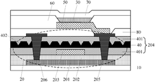
Specifically, as shown in FIG. 1, the OLED includes a base substrate 10, and a thin-film transistor 20, a first electrode 50, and a light-emitting layer 30 which are arranged on the base substrate 10 in sequence; the thin-film transistor 20 includes an active layer 201; and the OLED substrate further includes a light-shielding layer 40 arranged between the active layer 201 and the first electrode 50.
In the OLED substrate and the display device of the embodiment of the present disclosure, since the OLED substrate further includes a light-shielding layer arranged between the active layer and the first electrode, the light-shielding layer may block light emitted from the light-emitting layer, to prevent the light emitted by the layer from being incident on the active layer and thus affecting the characteristics of the thin-film transistor. Therefore, the present disclosure stabilizes the light-emitting characteristics of the OLED substrate and increases the light-emitting stability. In addition, the light-shielding layer can not only block the ambient light incident on the OLED substrate, but also shield the light emitted from the light-emitting layer. This prevents ambient light from being emitted onto the active layer, thereby preventing from affecting the characteristics of the thin-film transistor.
The thin-film transistor 20 includes a gate electrode 203, a gate insulating layer (GI) 202, a source electrode 206, and a drain electrode 205, in addition to the active layer 201. The source electrode 206 and the drain electrode 205 are in contact with the active layer 201 through the via hole, and the drain electrode 205 of the thin-film transistor 20 is electrically connected to the first electrode 50. Further, the thin-film transistor 20 may further include a film layer, such as an interlayer dielectric layer (ILD) 204.
The type of the thin-film transistor 20 is not limited. The thin-film transistor 20 may be, for example, an amorphous silicon (a-Si) thin-film transistor, a single crystal silicon thin-film transistor, or a low temperature poly-silicon thin-film transistor. Since the low temperature poly-silicon thin-film transistor has advantages of high mobility, reducing response time, reducing power consumption, and increasing resolution and contrast, a low temperature poly-silicon thin-film transistor is often selected as the thin-film transistor 20 in the organic electro-luminescent device. Low temperature poly-silicon is more sensitive to light than amorphous silicon and single crystal silicon. Therefore, the characteristics of the low temperature poly-silicon thin-film transistor are more susceptible to illumination.
The OLED substrate includes a pixel definition layer (PDL) 60 arranged between the first electrode 50 and the light-emitting layer 30 and a second electrode 70 arranged on the light-emitting layer 30, in addition to the thin-film transistor 20, the first electrode 50, and the light-emitting layer 30 which are arranged on the base substrate 10 in sequence, as shown in FIG. 1. The pixel defining layer 60 is divided into an open area and a pixel defining area for defining an open area. The light-emitting layer 30 is located in an open area of the pixel defining layer 60. The first electrode 50 and the second electrode 70 are used to drive the light-emitting layer 30 to emit light. In addition, the first electrode 50 may be an anode, and the second electrode 70 may be a cathode; or the first electrode 50 may be a cathode, and the second electrode 70 may be an anode.
Further, the OLED substrate may further include at least one of an electron transport layer, an electron injection layer, a hole transport layer, and a hole injection layer arranged between the first electrode 50 and the second electrode 70.
Generally, as shown in FIG. 1, the OLED substrate is further provided with a planarization layer (PLN) 80 between the thin-film transistor 20 and the first electrode 50.
Based on the above, the preparation process of the OLED substrate may specifically include: firstly forming a thin-film transistor 20 on the substrate 10, forming a planarization 80 on the thin-film transistor 20, and then forming the first electrode 50, the pixel defining layer 60, and the light-emitting layer 30 and second electrode 70 in sequence.
The installation position of the light-shielding layer 40 is not limited, as long as it is arranged between the active layer 201 and the first electrode 50.
In addition, the light-shielding layer 40 can be shared with the film layer originally present on the OLED substrate. For example, as shown in FIG. 2, the light-shielding layer 40 is shared with the interlayer dielectric layer 204 in the thin-film transistor 20, or the light-shielding layer 40 is shared with the gate insulating layer 202 in the thin-film transistor 20. That is, the interlayer dielectric layer 204 or the gate insulating layer 202 in the thin-film transistor 20 is also used as the light-shielding layer 40. As shown in FIG. 1, the light-shielding layer 40 may be additionally formed, that is, the light-shielding layer 40 is a layer different from the insulating layer such as the interlayer dielectric layer 204 or the gate insulating layer 202.
Optionally, the light-shielding layer 40 may be a light-absorbing layer. At this time, the material for preparing the light-shielding layer 40 may be, for example, a black ink or a black resin. Optionally, the light-shielding layer 40 may also be a reflective layer. At this time, the material for preparing the light-shielding layer 40 may be, for example, a metal material. The reflective layer reflects the light emitted by the light-emitting layer 30 or the ambient light that is incident thereon, and the excessive reflected light affects the light-emitting effect of the OLED substrate. Therefore, the light-shielding layer 40 of the embodiment of the present disclosure is preferably a light-absorbing layer.
As shown in FIG. 3, a buffer layer 90 may be arranged between the base substrate 10 and the thin-film transistor 20. The buffer layer 90 can not only flatten the base substrate 10 and shield the defects of the substrate 10, but also prevent impurity ions from penetrating into the base substrate 10 to cause various defects of the device.
Optionally, the material for preparing the light-shielding layer 40 includes amorphous silicon. As shown in FIG. 4, the OLED substrate further includes side layers 401 arranged on the upper and lower surface sides of the light-shielding layer 40 and in contact with the light-shielding layer 40. The material for the side layer 401 is an insulating material. Amorphous silicon has a greater absorption to visible light, especially to short-wavelength visible light. Therefore, when the material of the light-shielding layer 40 includes amorphous silicon, the light-shielding layer 40 corresponds to the light-absorbing layer, and visible light can be absorbed.
It should be noted that the light-shielding layer 40 provided in the OLED substrate of the embodiment of the present disclosure should not affect the performance of other film layers or devices; when the material of the light-shielding layer 40 includes amorphous silicon of a semiconductor material, in order to avoid the influence of amorphous silicon on the performance of other film layers, such that upper and lower side layers 401, which are in contact with the light-shielding layer 40, are arranged on the upper and lower sides of the amorphous silicon layer.
Optionally, the material for preparing the side layer 401 is an insulating material. The material of the side layers 401 may be, for example, at least one of silicon oxide (SiOx), silicon nitride (SiNx), or silicon oxynitride (SiOxNy).
Optionally, the thicknesses of the light-shielding layer 40 and the upper and lower side layers 401 are not limited. Optionally, the thickness of the light-shielding layer may be 2000 Å to 5000 Å. Optionally, one of the upper and lower side layers 401 may have a thickness of 1000 Å to 3000 Å. Further, when the upper and lower side layers 401 are made of silicon oxide, one of the upper and lower side layers 401 may have a thickness of 1000 Å to 3000 Å; and when the upper and lower side layers 401 are made of silicon nitride, the upper and lower side layers 401 have a thickness of 2000 Å to 3000 Å.
Since the material for preparing the light-shielding layer 40 is amorphous silicon, the light-shielding layer 40 can absorb the light emitted from the light-emitting layer 30 and block the light emitted from the light-emitting layer 30 from being incident on the active layer 201, thereby preventing form affecting the characteristics of the thin-film transistor. In addition, the light-shielding layer 40 can also absorb external ambient light incident into the OLED substrate, thereby preventing the excessive reflected light, after the external ambient light and the light emitted by the light-emitting layer 30 is reflected by the film layer in the OLED substrate, from affecting the light-emitting effect.
When the material for preparing the light-shielding layer 40 includes amorphous silicon, although amorphous silicon can absorb visible light, amorphous silicon still has a transmittance of about 30% to 70% for long-wavelength visible light (for example, red light and green light). Optionally, the material for preparing the light-shielding layer 40 further includes sulfur (S) doped in amorphous silicon. It should be noted that after sulfur is doped into a-Si, the light-absorbing performance of the light-shielding layer 40 is increased, and the reason why the addition of sulfur increases the light-absorbing performance is that an impurity state contributed by the dopant atoms appears below the conduction band of the a-Si, so that the band is narrowed. After doping sulfur in a-Si, a Si—S bond is formed. According to the simulation calculation, after the sulfur is doped in a-Si, the band of a-Si is changed from about 1.7 eV to about 0.551 eV. In addition, the 3 s state of S appears in the conduction band portion, and the 3 p state of S increases in the valence band portion. This change in energy band can increase the range and intensity of light absorption, and the band of absorbed light can be expanded to 250 nm to 1000 nm (390 to 780 nm in the visible region), in which the absorption range includes the UV-NIR region.
There is no limitation on how to allow the material for preparing light-shielding layer 40 to contain amorphous silicon and sulfur doped in amorphous silicon. Two specific implementations are provided below as examples. First, the amorphous silicon and the sulfur are first doped and mixed, and then the light-shielding layer 40 is formed. Second, an amorphous silicon layer is formed first, and then an amorphous silicon layer is etched by using SF6 (sulfur hexafluoride). Thus, in the etching process of SF6, sulfur element is doped into the amorphous silicon layer, thereby allowing the material for preparing light-shielding layer 40 to contain amorphous silicon and sulfur doped in amorphous silicon.
The content of sulfur doped in the amorphous silicon is not limited, and an appropriate amount of sulfur may be doped into the amorphous silicon as needed. If the content of sulfur doped in the amorphous silicon is too small, the improvement in the light-absorbing effect of the light-shielding layer 40 is not obvious. The light-absorbing effect of the light-shielding layer 40 gradually increases as the content of sulfur doped in the amorphous silicon increases. However, when the sulfur content is increased to a certain extent, the light-absorbing effect of the light-shielding layer 40 does not increase. Therefore, the mass of sulfur in the embodiment of the present disclosure is preferably 0.5% to 5% based on the total mass of the material of the light-shielding layer 40.
When the material of the light-shielding layer 40 includes amorphous silicon, doping sulfur in the amorphous silicon improves the light-absorbing efficiency and the light-absorbing intensity of the light-shielding layer 40, thereby enhancing the light-shielding effect of the light-shielding layer 40.
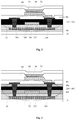
Optionally, as shown in FIGS. 5(a) and 5(b), the light-shielding layer 40 includes a plurality of depression portions 402 on a side proximate to the light-emitting layer 30.
The cross-sectional shape of the depression portion 402 taken along the thickness direction of the OLED substrate is not limited. The cross-sectional shape of the depression portion 402 may be a triangle as shown in FIGS. 5(a) and 5(b), or a trapezoidal, semi-circular shape (in which a semicircle is not shown in the drawing), or the like.
In addition, the plurality of depression portions 402 arranged on a side proximate to the light-emitting layer 30 may be distributed in a dot shape on the light-shielding layer 40 or may be distributed in a strip shape on the light-shielding layer 40.
The depression depth of the depression portion 402 is not limited, and may be set as needed. The depression portion 402 may not penetrate the light-shielding layer 40 as shown in FIG. 5(a), or may penetrate the light-shielding layer 40 as shown in FIG. 5(b). When the depression portion 402 does not penetrate the light-shielding layer 40, the light is incident on the depression portion 402 and passes through the remaining thickness of the light-shielding layer 40, thereby further ensuring the absorption of light. Therefore, the depression portion 402 of the embodiment of the present disclosure preferably does not penetrate the light-shielding layer 40. When the depression portion 402 does not penetrate the light-shielding layer 40, the light-shielding layer 40 includes the first light-shielding sublayer and the second light-shielding sublayer which are laminated. The first light-shielding sublayer is provided with a depression portion 402, and the thickness of the first light-shielding sublayer is the same as the depression depth of the depression portion 402. The thickness of the second light-shielding sublayer is not limited. In an optional embodiment of the present disclosure, the second light-shielding sublayer has a thickness of 100 to 900 Å.
The formation of the depression portion 402 on the side of the light-shielding layer 40 proximate to the light-emitting layer 30 is not limited. A light-shielding layer film can be formed first. For example, the light-shielding layer film may be formed by a deposition method, and the light-shielding layer film may be exposed, developed, and etched, for example, by a dry etch process, to form the light-shielding layer 40. That is, a plurality of depression portions 402 is formed on the light-shielding layer film by an incomplete etching method.
It should be noted that when the light-shielding layer 40 includes a plurality of depression portions 402 on the side proximate to the light-emitting layer 30, and the material for preparing the light-shielding layer 40 is amorphous silicon, as shown in FIG. 6, the lower side layer 401 may be deposited first, a light-shielding layer thin film is further formed, and the light-shielding layer thin film is patterned to form the light-shielding layer 40, and then the upper side layer 401 is further formed on the light-shielding layer 40, as shown in FIG. 7.
In the embodiment of the present disclosure, since the light-shielding layer 40 includes a plurality of depression portions 402 on a side proximate to the light-emitting layer 30, the depression portion 402 facilitates the falling of the incident light and reduces the reflected light, thereby improving the light-absorbing effect of the light-shielding layer 40.
Since the cross-sectional shape of the depression portion 402 obtained after the light-shielding layer 40 is cut along the thickness direction of the OLED substrate is a triangle, as shown in FIG. 8, after the incident light is incident on the depression portion 402, a portion of the light is reflected, and a portion of the light is refracted. The refracted light is absorbed. After the incident light is reflected and refracted multiple times, the intensity of the light finally reflected from the light-shielding layer 40 is greatly weakened, thereby effectively improving the light-absorbing effect of the light-shielding layer 40. Therefore, as shown in FIGS. 5(a) and 5(b), the cross-sectional shape of the depression portion 402 obtained by taking the light-shielding layer 40 along the thickness direction of the OLED substrate is preferably a triangle.
When the cross-sectional shape of the depression portion 402 obtained by taking the light-shielding layer 40 along the thickness direction of the OLED substrate is a triangle, the depression portion 402 may be distributed in a dot shape on the light-shielding layer 40 or may be distributed in a strip shape on the light-shielding layer 40. Optionally, the depression portions 402 are distributed in a dot shape on the light-shielding layer 40. Further optionally, when the depression portion 402 is distributed in a dot shape on the light-shielding layer 40, the depression portion 402 has a conical structure.
Optionally, the thin-film transistor 20 further includes an insulating layer arranged on a side of the active layer 201 proximate to the light-emitting layer 30. Optionally, the OLED substrate further includes a planarization layer 80 arranged between the thin-film transistor 20 and the first electrode 50. Optionally, the light-shielding layer 40 is shared with the insulating layer or the planarization layer 80, that is, the insulating layer and the planarization are also used as the light-shielding layer.
It should be noted that, in the case where the light-shielding layer 40 is shared with the insulating layer, the thin-film transistor 20, as shown in FIG. 2, includes the active layer 201, the gate insulating layer 202, the gate electrode 203, and the interlayer dielectric layer 204, the source electrode 206, and the drain electrode 205, which are arranged in sequence. At this time, since the insulating layer of the thin-film transistor 20 may be the gate insulating layer 202 or the interlayer dielectric layer 204, the light-shielding layer 40 may be shared with the gate insulating layer 202, or shared with the light-shielding layer 40 and the interlayer dielectric layer 204 as shown in FIGS. 2 and 3. When the thin-film transistor includes the active layer 201, the source electrode 206, the drain electrode 205, the gate insulating layer 202, and the gate electrode 203 which are arranged in sequence, the insulating layer of the thin-film transistor 20 is the gate insulating layer 202, and thus the light-shielding layer 40 is shared with the gate insulating layer 202.
When the light-shielding layer 40 is shared with the insulating layer, the light-shielding layer 40 should serve both as a function of light-shielding and as a function of insulation. When the light-shielding layer 40 is shared with the planarization layer 80, the light-shielding layer 40 should serve both as a function of light-shielding and as a function of flattening.
In an optional embodiment of the present disclosure, by sharing the light-shielding layer 40 with the insulating layer of the planarization layer 80 or the thin-film transistor 20, the step of separately forming the light-shielding layer can be reduced as compared with additionally providing the light-shielding layer 40. This simplifies the preparation process of the OLED substrate.
Optionally, the thin-film transistor 20 further includes an insulating layer arranged on a side of the active layer 201 proximate to the light-emitting layer 30. Optionally, the OLED substrate further includes a planarization layer 80 arranged between the thin-film transistor 20 and the first electrode 50. Optionally, the light-shielding layer 40 and the two side layers 401 are combined with the insulating layer or shared with the planarization layer 80, that is, the two side layers 401 and the insulating layer are also used integrally as the light-shielding layer 40, or the planarization layer 80 is also used as the light-shielding layer.
It should be noted that, in the case where the light-shielding layer 40 and two side layers 401 are shared with the insulating layer, the thin-film transistor 20, as shown in FIG. 2, includes the active layer 201, the gate insulating layer 202, the gate electrode 203, and the interlayer dielectric layer 204, the source electrode 206, and the drain electrode 205, which are arranged in sequence. At this time, since the insulating layer of the thin-film transistor 20 may be the gate insulating layer 202 or the interlayer dielectric layer 204, the light-shielding layer 40 and two side layers 401 may be shared with the gate insulating layer 202, or shared with the light-shielding layer 40 and two side layers 401 as shown in FIGS. 4, 5(a), 5(b), 7 and 9. When the thin-film transistor includes the active layer 201, the source electrode 206, the drain electrode 205, the gate insulating layer 202, and the gate electrode 203 which are arranged in sequence, the insulating layer of the thin-film transistor 20 is the gate insulating layer 202, and thus the light-shielding layer 40 and the two side layers 401 are shared with the gate insulating layer 202.
When the thin-film transistor 20 includes the active layer 201, the gate insulating layer 202, the gate electrode 203, the interlayer dielectric layer 204, the source electrode 206, and the drain electrode 205, which are arranged in sequence, the process for preparing the thin-film transistor includes: after the forming the gate insulating layer 202, the gate electrode 203 and the interlayer dielectric layer 204 in sequence, as shown in FIG. 9 (in FIG. 9, the light-shielding layer 40 and the two side layers 401 are shared with the interlayer dielectric layer 204 as an example), a dielectric layer 204 and a gate insulating layer 202 are exposed, developed, and etched to form a source contact via hole and a drain contact via hole, and then a source electrode 206 and a drain electrode 205 are formed. The source electrode 206 is in contact with the active layer 201 through a source contact hole, and the drain electrode 205 is in contact with the active layer 201 through a drain contact hole.
When the light-shielding layer 40 and the two upper and lower side layers 401 are shared with the insulating layer, the light-shielding layer 40 and the two upper and lower side layers 401 should serve both as a function of light-shielding and as a function of insulation; and when the light-shielding layer 40 and the two upper and lower side layers 401 are shared with the planarization 80, the light-shielding layer 40 and the two upper and lower side layers 401 should serve both as a function of light-shielding and as a function of flattening.
In the embodiment of the present disclosure, by sharing the light-shielding layer 40 and the two upper and lower side layers 401 with the planarization layer 80 or the insulating layer of the thin-film transistor 20, the step of forming one light-shielding layer can be reduced as compared with the additional providing the light-shielding layer 40. This simplifies the preparation process of the OLED substrate.
Another embodiment of the present disclosure further provides a display device including any of the above OLED substrates.
The display device may be any device that displays an image regardless of being movable (e.g., video) or fixed (e.g., still image) and regardless of text or picture. More specifically, it is expected that the described embodiments can be implemented in or associated with various electronic devices. The various electronic devices include, but not limited to, mobile phones, wireless devices, personal data assistants (PDA), handheld or portable computers, GPS receivers/navigators, cameras, MP4 video players, video cameras, game consoles, watches, clocks, calculators, television monitors, flat panel displays, computer monitors, car displays (e.g., odometer display, etc.), navigator, cockpit controller and/or displays, camera view displays (e.g., displays for a rear-view camera in a vehicle) electronic photographs, electronic billboards or signs, projectors, architectural structures, packaging and aesthetic structures (e.g., displays for images of a piece of jewelry), etc. Further, the display device may also be a display panel.
The display device includes a package film or a package substrate for packaging the OLED substrate, in addition to the OLED substrate.
A display device according to one embodiment of the present disclosure includes the above-described OLED substrate. The OLED substrate in the display device has the same technical features and advantageous effects as the OLED substrate described above. Since the technical features and advantageous effects of the OLED substrate have been described in detail above, they will be not described herein again.
The above description is merely the optional embodiment of the present disclosure, but the scope of the present disclosure is not limited thereto. Moreover, any person skilled in the art would readily conceive of modifications or substitutions within the technical scope of the present disclosure, and these modifications or substitutions shall also fall within the protection scope of the present disclosure. Therefore, the protection scope of the present disclosure should be determined by the scope of the claims.

Claims (16)

What is claimed is:
1. An organic light-emitting diode (OLED) substrate, comprising a base substrate, and a thin-film transistor, a first electrode, and a light-emitting layer arranged in sequence on the base substrate, wherein the OLED substrate further comprises a light-shielding layer arranged between an active layer of the thin-film transistor and the first electrode,
wherein a material of the light-shielding layer comprises amorphous silicon, and the OLED substrate further comprises side layers arranged on two opposite sides of the light-shielding layer and in contact with the light-shielding layer, and wherein a material of the side layers is an insulating material,
wherein the material of the light-shielding layer further comprises sulfur doped in the amorphous silicon.
2. The OLED substrate of claim 1, wherein the sulfur has a mass ratio of 0.5% to 5% based on the total mass of the material of the light-shielding layer.
3. The OLED substrate of claim 1, wherein the light-shielding layer comprises a plurality of depression portions on a side proximate to the light-emitting layer.
4. The OLED substrate of claim 3, wherein a cross-sectional shape of the depression portion obtained by cutting the light-shielding layer along a thickness direction of the OLED substrate is a triangle.
5. The OLED substrate of claim 4, wherein the depression portion does not penetrate through the light-shielding layer.
6. The OLED substrate of claim 1, wherein the light-shielding layer comprises a plurality of depression portions on a side proximate to the light-emitting layer.
7. The OLED substrate of claim 6, wherein a cross-sectional shape of the depression portion obtained by cutting the light-shielding layer along a thickness direction of the OLED substrate is a triangle.
8. The OLED substrate of claim 7, wherein the depression portion does not penetrate through the light-shielding layer.
9. The OLED substrate of claim 1, wherein the thin-film transistor further comprises an insulating layer arranged on a side of the active layer proximate to the light-emitting layer, the OLED substrate further comprises a planarization layer between the thin-film transistor and the first electrode, and the insulating layer or the planarization layer is also used as a light-shielding layer.
10. The OLED substrate of claim 1, wherein the thin-film transistor further comprises an insulating layer arranged on a side of the active layer proximate to the light-emitting layer, the OLED substrate further comprises a planarization layer between the thin-film transistor and the first electrode, and the side layers and the insulating layer are also used as a light-shielding layer as a whole, or the planarization layer is also used as a light-shielding layer.
11. A display device comprising the OLED substrate of claim 1.
12. The display device of claim 11, wherein the sulfur has a mass ratio of 0.5% to 5% based on the total mass of the material of the light-shielding layer.
13. The display device of claim 11, wherein the light-shielding layer comprises a plurality of depression portions on a side proximate to the light-emitting layer.
14. The display device of claim 13, wherein a cross-sectional shape of the depression portion obtained by cutting the light-shielding layer along a thickness direction of the OLED substrate is a triangle.
15. The display device of claim 13, wherein the depression portion does not penetrate through the light-shielding layer.
16. The display device of claim 11, wherein the thin-film transistor further comprises an insulating layer arranged on a side of the active layer proximate to the light-emitting layer, the OLED substrate further comprises a planarization layer between the thin-film transistor and the first electrode, and the insulating layer or the planarization layer is also used as a light-shielding layer.
US16/446,067 2018-07-13 2019-06-19 OLED substrate and display device Active US10692952B2 (en)

Applications Claiming Priority (3)

Application Number Priority Date Filing Date Title
CN201810772090.4A CN108987595A (en) 2018-07-13 2018-07-13 A kind of oled substrate and display device
CN201810772090.4 2018-07-13
CN201810772090 2018-07-13

Publications (2)

Publication Number Publication Date
US20200020757A1 US20200020757A1 (en) 2020-01-16
US10692952B2 true US10692952B2 (en) 2020-06-23

Family

ID=64537539

Family Applications (1)

Application Number Title Priority Date Filing Date
US16/446,067 Active US10692952B2 (en) 2018-07-13 2019-06-19 OLED substrate and display device

Country Status (2)

Country Link
US (1) US10692952B2 (en)
CN (1) CN108987595A (en)

Families Citing this family (12)

* Cited by examiner, † Cited by third party
Publication number Priority date Publication date Assignee Title
KR102454468B1 (en) * 2017-09-20 2022-10-14 주식회사 디비하이텍 Signal control unit for an organic light emitting diode display device, method of manufacturing the same, and organic light emitting diode including the same
CN109786323A (en) * 2019-01-16 2019-05-21 深圳市华星光电半导体显示技术有限公司 The preparation method and tft array substrate of tft array substrate
CN110071149B (en) * 2019-04-15 2021-05-18 昆山工研院新型平板显示技术中心有限公司 Display panel and display device
CN110335883B (en) * 2019-04-25 2021-09-28 昆山工研院新型平板显示技术中心有限公司 Display panel and display device
US11765924B2 (en) * 2019-12-19 2023-09-19 Lg Display Co., Ltd. Light emitting display panel and light emitting display apparatus including the same
KR102830070B1 (en) * 2019-12-19 2025-07-04 엘지디스플레이 주식회사 Light emitting display panel and light emitting display appartus using the same
CN111584604A (en) 2020-05-28 2020-08-25 京东方科技集团股份有限公司 OLED display substrate, method for making the same, and display device
EP4156277A4 (en) 2020-06-08 2023-11-15 Guangdong Oppo Mobile Telecommunications Corp., Ltd. Display device, processing method therefor, and electronic device
CN111969033A (en) * 2020-08-31 2020-11-20 江苏仕邦柔性电子研究院有限公司 Flexible OLED display panel and flexible OLED display device
CN113644098B (en) * 2021-07-29 2023-11-21 合肥维信诺科技有限公司 Display panel, preparation method of display panel and display device
CN113764490B (en) * 2021-09-06 2023-05-09 深圳市华星光电半导体显示技术有限公司 OLED display panel
CN119744093B (en) * 2021-12-22 2025-12-09 武汉华星光电半导体显示技术有限公司 Display panel, display module and mobile terminal

Citations (6)

* Cited by examiner, † Cited by third party
Publication number Priority date Publication date Assignee Title
US20020038998A1 (en) 2000-09-29 2002-04-04 Yoshimasa Fujita Luminescent display device of active matrix drive type and fabrication method therefor
US20030116768A1 (en) * 2001-05-23 2003-06-26 Semiconductor Energy Laboratory Co., Ltd. Semiconductor device and manufacturing method thereof
US20050029926A1 (en) * 2003-08-07 2005-02-10 Park Sang-Ii Flat panel display and method of fabricating the same
CN102431957A (en) 2011-12-01 2012-05-02 中国科学院半导体研究所 Method for manufacturing non-refrigerant thermal infrared detector based on black silicon material
US20140159021A1 (en) * 2012-12-12 2014-06-12 Boe Technology Group Co., Ltd. Array substrate, method for fabricating the same, and oled display device
CN107046042A (en) 2017-04-20 2017-08-15 京东方科技集团股份有限公司 A kind of low temperature polycrystalline silicon backboard and its manufacture method, display device

Patent Citations (6)

* Cited by examiner, † Cited by third party
Publication number Priority date Publication date Assignee Title
US20020038998A1 (en) 2000-09-29 2002-04-04 Yoshimasa Fujita Luminescent display device of active matrix drive type and fabrication method therefor
US20030116768A1 (en) * 2001-05-23 2003-06-26 Semiconductor Energy Laboratory Co., Ltd. Semiconductor device and manufacturing method thereof
US20050029926A1 (en) * 2003-08-07 2005-02-10 Park Sang-Ii Flat panel display and method of fabricating the same
CN102431957A (en) 2011-12-01 2012-05-02 中国科学院半导体研究所 Method for manufacturing non-refrigerant thermal infrared detector based on black silicon material
US20140159021A1 (en) * 2012-12-12 2014-06-12 Boe Technology Group Co., Ltd. Array substrate, method for fabricating the same, and oled display device
CN107046042A (en) 2017-04-20 2017-08-15 京东方科技集团股份有限公司 A kind of low temperature polycrystalline silicon backboard and its manufacture method, display device

Non-Patent Citations (1)

* Cited by examiner, † Cited by third party
Title
First Office Action for Chinese Application No. 201810772090.4, dated Sep. 4, 2019, 5 Pages.

Also Published As

Publication number Publication date
US20200020757A1 (en) 2020-01-16
CN108987595A (en) 2018-12-11

Similar Documents

Publication Publication Date Title
US10692952B2 (en) OLED substrate and display device
JP7187602B2 (en) light emitting device
US11315977B2 (en) Photosensitive assembly and method for preparing the same, array substrate, and display device
US9685489B2 (en) OLED pixel structure and OLED display device
JP2025128213A (en) Semiconductor Devices
TWI574391B (en) Semiconductor device and method of manufacturing same
TWI535016B (en) Semiconductor device and method of manufacturing semiconductor device
US11271049B2 (en) Array substrate, preparation method thereof and related device
KR20190054040A (en) Semiconductor device
WO2019148886A1 (en) Array substrate and manufacturing method thereof, and corresponding display device
US11121226B2 (en) Thin film transistor and method for manufacturing the same, array substrate and display device
US20220149137A1 (en) Display substrate, method for manufacturing same, and display apparatus
TW201743455A (en) Semiconductor device and method of manufacturing semiconductor device
TW201332022A (en) Semiconductor device and method of manufacturing semiconductor device
US7902640B2 (en) Dielectric layer and thin film transistor
US20170352711A1 (en) Manufacturing method of tft backplane and tft backplane
CN106887438B (en) Array substrate, manufacturing method thereof and display device
US20240276850A1 (en) Display panel and mobile terminal
CN108257975B (en) Array substrate and preparation method thereof, display device and preparation method of thin film transistor
US11329194B2 (en) Display panel and display device
KR20170081060A (en) Thin film transistor and thin film transistor substrate having the same
CN110911455B (en) Display panel and display device
WO2015046204A1 (en) Tft array substrate, liquid crystal display device and method for producing tft array substrate

Legal Events

Date Code Title Description
AS Assignment

Owner name: BOE TECHNOLOGY GROUP CO., LTD., CHINA

Free format text: ASSIGNMENT OF ASSIGNORS INTEREST;ASSIGNORS:LI, HAIXU;CAO, ZHANFENG;REEL/FRAME:049523/0452

Effective date: 20190328

FEPP Fee payment procedure

Free format text: ENTITY STATUS SET TO UNDISCOUNTED (ORIGINAL EVENT CODE: BIG.); ENTITY STATUS OF PATENT OWNER: LARGE ENTITY

STPP Information on status: patent application and granting procedure in general

Free format text: NON FINAL ACTION MAILED

STPP Information on status: patent application and granting procedure in general

Free format text: NOTICE OF ALLOWANCE MAILED -- APPLICATION RECEIVED IN OFFICE OF PUBLICATIONS

STPP Information on status: patent application and granting procedure in general

Free format text: PUBLICATIONS -- ISSUE FEE PAYMENT VERIFIED

STCF Information on status: patent grant

Free format text: PATENTED CASE

MAFP Maintenance fee payment

Free format text: PAYMENT OF MAINTENANCE FEE, 4TH YEAR, LARGE ENTITY (ORIGINAL EVENT CODE: M1551); ENTITY STATUS OF PATENT OWNER: LARGE ENTITY

Year of fee payment: 4