US10692831B1 - Stud bumps for post-measurement qubit frequency modification - Google Patents
Stud bumps for post-measurement qubit frequency modification Download PDFInfo
- Publication number
- US10692831B1 US10692831B1 US16/281,770 US201916281770A US10692831B1 US 10692831 B1 US10692831 B1 US 10692831B1 US 201916281770 A US201916281770 A US 201916281770A US 10692831 B1 US10692831 B1 US 10692831B1
- Authority
- US
- United States
- Prior art keywords
- chip
- metallic
- qubit
- test
- interposer
- Prior art date
- Legal status (The legal status is an assumption and is not a legal conclusion. Google has not performed a legal analysis and makes no representation as to the accuracy of the status listed.)
- Active
Links
Images


Classifications
-
- H—ELECTRICITY
- H01—ELECTRIC ELEMENTS
- H01L—SEMICONDUCTOR DEVICES NOT COVERED BY CLASS H10
- H01L24/00—Arrangements for connecting or disconnecting semiconductor or solid-state bodies; Methods or apparatus related thereto
- H01L24/01—Means for bonding being attached to, or being formed on, the surface to be connected, e.g. chip-to-package, die-attach, "first-level" interconnects; Manufacturing methods related thereto
- H01L24/10—Bump connectors ; Manufacturing methods related thereto
- H01L24/12—Structure, shape, material or disposition of the bump connectors prior to the connecting process
- H01L24/14—Structure, shape, material or disposition of the bump connectors prior to the connecting process of a plurality of bump connectors
-
- H10P74/23—
-
- G—PHYSICS
- G06—COMPUTING OR CALCULATING; COUNTING
- G06N—COMPUTING ARRANGEMENTS BASED ON SPECIFIC COMPUTATIONAL MODELS
- G06N10/00—Quantum computing, i.e. information processing based on quantum-mechanical phenomena
-
- G—PHYSICS
- G06—COMPUTING OR CALCULATING; COUNTING
- G06N—COMPUTING ARRANGEMENTS BASED ON SPECIFIC COMPUTATIONAL MODELS
- G06N10/00—Quantum computing, i.e. information processing based on quantum-mechanical phenomena
- G06N10/40—Physical realisations or architectures of quantum processors or components for manipulating qubits, e.g. qubit coupling or qubit control
-
- G—PHYSICS
- G06—COMPUTING OR CALCULATING; COUNTING
- G06N—COMPUTING ARRANGEMENTS BASED ON SPECIFIC COMPUTATIONAL MODELS
- G06N10/00—Quantum computing, i.e. information processing based on quantum-mechanical phenomena
- G06N10/70—Quantum error correction, detection or prevention, e.g. surface codes or magic state distillation
-
- H—ELECTRICITY
- H01—ELECTRIC ELEMENTS
- H01L—SEMICONDUCTOR DEVICES NOT COVERED BY CLASS H10
- H01L22/00—Testing or measuring during manufacture or treatment; Reliability measurements, i.e. testing of parts without further processing to modify the parts as such; Structural arrangements therefor
- H01L22/10—Measuring as part of the manufacturing process
- H01L22/12—Measuring as part of the manufacturing process for structural parameters, e.g. thickness, line width, refractive index, temperature, warp, bond strength, defects, optical inspection, electrical measurement of structural dimensions, metallurgic measurement of diffusions
-
- H—ELECTRICITY
- H01—ELECTRIC ELEMENTS
- H01L—SEMICONDUCTOR DEVICES NOT COVERED BY CLASS H10
- H01L22/00—Testing or measuring during manufacture or treatment; Reliability measurements, i.e. testing of parts without further processing to modify the parts as such; Structural arrangements therefor
- H01L22/20—Sequence of activities consisting of a plurality of measurements, corrections, marking or sorting steps
- H01L22/22—Connection or disconnection of sub-entities or redundant parts of a device in response to a measurement
-
- H—ELECTRICITY
- H01—ELECTRIC ELEMENTS
- H01L—SEMICONDUCTOR DEVICES NOT COVERED BY CLASS H10
- H01L23/00—Details of semiconductor or other solid state devices
- H01L23/48—Arrangements for conducting electric current to or from the solid state body in operation, e.g. leads, terminal arrangements ; Selection of materials therefor
- H01L23/488—Arrangements for conducting electric current to or from the solid state body in operation, e.g. leads, terminal arrangements ; Selection of materials therefor consisting of soldered or bonded constructions
- H01L23/498—Leads, i.e. metallisations or lead-frames on insulating substrates, e.g. chip carriers
- H01L23/49811—Additional leads joined to the metallisation on the insulating substrate, e.g. pins, bumps, wires, flat leads
-
- H—ELECTRICITY
- H01—ELECTRIC ELEMENTS
- H01L—SEMICONDUCTOR DEVICES NOT COVERED BY CLASS H10
- H01L23/00—Details of semiconductor or other solid state devices
- H01L23/58—Structural electrical arrangements for semiconductor devices not otherwise provided for, e.g. in combination with batteries
- H01L23/64—Impedance arrangements
- H01L23/66—High-frequency adaptations
-
- H—ELECTRICITY
- H01—ELECTRIC ELEMENTS
- H01L—SEMICONDUCTOR DEVICES NOT COVERED BY CLASS H10
- H01L24/00—Arrangements for connecting or disconnecting semiconductor or solid-state bodies; Methods or apparatus related thereto
- H01L24/80—Methods for connecting semiconductor or other solid state bodies using means for bonding being attached to, or being formed on, the surface to be connected
- H01L24/81—Methods for connecting semiconductor or other solid state bodies using means for bonding being attached to, or being formed on, the surface to be connected using a bump connector
-
- H—ELECTRICITY
- H01—ELECTRIC ELEMENTS
- H01L—SEMICONDUCTOR DEVICES NOT COVERED BY CLASS H10
- H01L24/00—Arrangements for connecting or disconnecting semiconductor or solid-state bodies; Methods or apparatus related thereto
- H01L24/93—Batch processes
- H01L24/95—Batch processes at chip-level, i.e. with connecting carried out on a plurality of singulated devices, i.e. on diced chips
- H01L24/97—Batch processes at chip-level, i.e. with connecting carried out on a plurality of singulated devices, i.e. on diced chips the devices being connected to a common substrate, e.g. interposer, said common substrate being separable into individual assemblies after connecting
-
- H—ELECTRICITY
- H10—SEMICONDUCTOR DEVICES; ELECTRIC SOLID-STATE DEVICES NOT OTHERWISE PROVIDED FOR
- H10N—ELECTRIC SOLID-STATE DEVICES NOT OTHERWISE PROVIDED FOR
- H10N69/00—Integrated devices, or assemblies of multiple devices, comprising at least one superconducting element covered by group H10N60/00
-
- H10P74/203—
-
- H10P74/207—
-
- H10P74/232—
-
- H10W44/20—
-
- H10W72/0198—
-
- H10W72/072—
-
- H10W72/20—
-
- H10W90/701—
-
- H10W72/01225—
-
- H10W72/07253—
-
- H10W72/221—
-
- H10W72/227—
-
- H10W72/237—
-
- H10W72/241—
-
- H10W72/248—
-
- H10W72/29—
-
- H10W72/90—
-
- H10W72/9415—
-
- H10W72/952—
-
- H10W90/724—
Definitions
- the present invention relates to methods of producing quantum computer chips and the chips produced, and more particularly to methods of producing quantum computer chips including post-measurement qubit frequency modification of the chips produced.
- post-measurement frequency modification often requires access to qubits on the qubit chip after the qubit chip is assembled on a substrate with readout circuits (or parts thereof).
- the qubit chip may be flip chip bonded to an interposer chip to perform measurements on the qubit chip, and to form a quantum-computer chip.
- the qubit chip is flip chip bonded to the interposer chip, it is no longer possible to access the qubit chip to perform frequency modification.
- a method of producing a quantum computer chip includes performing a frequency measurement on a qubit chip bonded to a test interposer chip for qubits on the qubit chip at an operating temperature of the qubit chip. The method further includes pulling the qubit chip apart from the test interposer chip after performing the frequency measurement, and modifying a frequency of a subset of qubits after pulling the qubit chip apart from the test interposer chip. The method further includes bonding the qubit chip to a device interposer chip after modifying the frequency of the subset of qubits.
- the method enables post-measurement modification of the qubit frequency by providing access to the qubit chip after the chip has been cooled and a measurement has been performed at low temperature.
- the low temperature frequency measurement is more accurate than room-temperature measurements that predict the frequency, and enables subsequent precise qubit frequency modification that prevents frequency collisions between qubits.
- FIG. 1 is a flowchart that illustrates a method of producing a quantum computer chip according to an embodiment of the current invention.
- FIG. 2 is a schematic illustration of a qubit chip according to an embodiment of the current invention.
- FIG. 3 is a schematic illustration of a test interposer chip according to an embodiment of the current invention.
- FIG. 4 is a schematic illustration of the bonded qubit chip and test interposer chip according to an embodiment of the invention.
- FIG. 5 is a schematic illustration of a device interposer chip according to an embodiment of the current invention.
- FIG. 6 is a schematic illustration of the bonded qubit chip and device interposer chip according to an embodiment of the invention.
- FIG. 7 is a schematic illustration of a qubit chip according to an embodiment of the invention.
- FIG. 8 is a schematic illustration of a qubit chip bonded to a test interposer.
- FIG. 9 is a schematic illustration of a device interposer chip according to an embodiment of the invention.
- FIG. 10 is a schematic illustration of the qubit chip bonded to the device interposer chip.
- FIG. 11 is a schematic illustration of a qubit chip according to an embodiment of the invention.
- FIG. 12 is a schematic illustration of a qubit chip bonded to a test interposer chip 1202 .
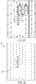
- FIG. 13 is a schematic illustration of a device interposer chip according to an embodiment of the invention.
- FIG. 14 is a schematic illustration of a qubit chip bonded to a device interposer chip 1402 .
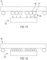
- FIG. 15 is a schematic drawing of an unbonded qubit chip and interposer chip.
- FIG. 16 is a schematic drawing of a bonded qubit chip and interposer chip.
- FIG. 17 is an image of metallic stud on a qubit chip after the qubit chip has been bonded to and pulled apart from a test interposer chip.
- FIG. 18 is a schematic illustration of a qubit chip bonded to an interposer chip.
- FIG. 19 is a schematic illustration of a qubit chip with gold studs and a qubit.
- FIG. 20 is a schematic illustration of a test interposer chip with test solder bumps.
- FIG. 21 is a schematic illustration of the qubit chip bonded to the test interposer chip.
- FIG. 22 is a schematic illustration of the qubit chip prior to bonding to the device interposer chip.
- FIG. 23 is a schematic illustration of a device interposer chip prior to bonding to the qubit chip.
- FIG. 24 is a schematic illustration of the qubit chip bonded to the device interposer chip.
- FIG. 1 is a flowchart that illustrates a method 100 of producing a quantum computer chip according to an embodiment of the current invention.
- the method 100 includes providing a qubit chip 102 , and providing a test interposer chip that has at least a portion of a readout circuit 104 .
- the method 100 further includes bonding the qubit chip to the test interposer chip 106 , and cooling the bonded qubit chip and test interposer chip to an operating temperature of the qubit chip 108 .
- more than one qubit chip can be bonded on a test interposer chip.
- the method 100 further includes performing a frequency measurement 110 on the cooled bonded qubit chip and test interposer chip for qubits on the qubit chip using the readout circuit.
- the method 100 further includes pulling the qubit chip apart from the test interposer chip 114 after performing the frequency measurement 110 .
- the method 100 further includes modifying a frequency of a subset of qubits 116 after pulling the qubit chip apart from the test interposer chip 114 , and bonding the qubit chip to a device interposer chip 118 after modifying the frequency of the subset of qubits 116 .
- more than one qubit chip can be bonded on a device interposer chip.
- the method does not include providing the qubit chip 102 , providing the test interposer chip 104 , bonding the qubit chip to the test interposer chip 106 , and cooling the bonded qubit chip and test interposer chip 108 .
- the qubit chip and test interposer chip may be fabricated and bonded beforehand, for example, by a manufacturer.
- the method may begin with performing the frequency measurement 110 on a qubit chip bonded to a test interposer chip.
- a qubit chip is a chip that includes a substrate and at least one quantum bit (qubit) formed thereon.
- the qubit may be a superconducting qubit.
- the qubit may include one or more Josephson junctions, for example.
- the qubit may be a transmon.
- the qubit chip includes superconducting wiring formed on the substrate.
- the qubit chip may include a thin under bump metallurgy (UBM) pad formed on the superconducting wiring that becomes superconducting by virtue of the proximity effect.
- the qubit chip includes a readout resonator or part of a readout resonator.
- an interposer chip is a chip that includes a substrate and superconducting wiring formed on the substrate.
- the interposer chip may include at least one thin UBM pad disposed on the metal interconnects that becomes superconducting by virtue of the proximity effect.
- the interposer chip includes a readout circuit.
- the readout circuit may be a readout resonator or part of a readout resonator, for example.
- the interposer chip may be a test interposer used for testing the qubits, or a device interposer chip to be incorporated into a quantum computing device.
- the device interposer chip is the test interposer chip reused.
- the device interposer chip is bonded to the qubit chip via cold welding.
- the qubits are coupled to each other by a physical connection, for example, capacitively or by coupling to a coplanar waveguide bus.
- a physical connection for example, capacitively or by coupling to a coplanar waveguide bus.
- the space on the qubit chip becomes a limiting factor. Moving the readout resonator or a portion of the readout resonator to the interposer chip enables more qubits to be formed on the qubit chip. Since this is true for the device interposer chip, it must also be true for the test interposer chip.
- Pulling the qubit chip apart from the test interposer chip means applying a force to at least one of the qubit chips and the test interposer chip to physically separate the qubit chip from the test interposer chip.
- the pulling will result in the breaking of bonds between studs on the qubit chip and solder bumps on the test interposer chip.
- some solder material from the solder bump may remain adhered to the stud after the pulling.
- the pulling does not require chemical treatment or annealing of the qubit chip. Consequently, the qubit chip and interposer chip are separated while avoiding damage to the qubits on the qubit chip.
- Low temperatures at which qubits may operate are defined as temperatures that are sufficiently below the critical temperatures of the superconductors involved and the temperature corresponding to the qubit transition frequency.
- Tc critical temperature
- k B T thermal energy
- a sufficiently low temperature is a temperature that is a small fraction of the lower of Tc and the temperature corresponding to the qubit transition frequency.
- the small fraction may be about 1/10, 1/15, or 1/20, for example.
- a temperature less than 20 mK can be sufficiently low.
- the frequency of the qubit corresponds to the transition energy between the two states of the qubit being used for computation.
- a qubit has two quantum states that are sufficiently separated in energy and/or decoupled from any additional quantum states so that the qubit is approximately a two-quantum state structure under operation conditions.
- the transition energy between the two states is a fixed quantity that defines the frequency of the qubit. For some qubits, the transition energy can nonetheless be modified, for example, by annealing the qubit with a laser.
- the method 100 enables the potential for frequency modification feedback because the method provides access to the Josephson junctions formed on the qubit chip after the frequency of the qubits has been measured.
- the qubit can be modified using any conventional method currently in existence or developed in the future.
- Non-lithographic modification of the qubits can be performed by laser annealing the Josephson junction and/or laser ablation of dielectric or conductive material, tribological modification (i.e., with a nanoindentor), or dry etching through a hard mask.
- Lithographic methods may also be used. In particular, lithographic methods with a thick resist and low bake temperature may be employed. Soft lithography may also be used.
- Negative resists that can be patterned greater than 100 ⁇ m, such as SU-8, KMPR, and JSR for spin on or spray on resists, can be used.
- a positive resist could also be used by spraying and exposing with a direct write laser. This would allow a thinner resist to be used, which would prevent the stud bumps from being covered. Also, positive resists may have lower bake temperatures.
- Direct access to the qubit surface enables inspection such as microscopy or electrical resistance measurements of junctions or other structures on the surface, to confirm the modification.
- the qubit frequencies may be modified only by techniques that penetrate either the interposer (above) or qubit substrate (below) without causing undesired damage. Such techniques will be more difficult, limited and imprecise than if the interposer is removed and the qubit surface is directly accessible.
- Performing laser annealing through the interposer chip requires the interposer chip to have a transparent substrate or machined windows.
- the transparent substrate or machined windows may require additional fabrication steps. Further, the transparent substrate may introduce two-level systems that decrease qubit coherence and reliability.
- the machined windows may have stress concentration and handling issues that reduce coherence and reliability.
- the qubit frequencies may be modified using backside qubit chip frequency modification, which requires a thinned qubit die.
- the thinned qubit die is susceptible to stress concentration and handling issues that can negatively impact coherence and reliability.
- the method 100 does not create coherence or reliability penalties. Further, the method 100 enables a more accurate final Josephson junction frequency prediction than other methods.
- the frequency of the qubits can be modified, for example, by laser annealing or ablation, based on the cold-temperature frequency predictions.
- the broad concepts of the current invention are not limited to only laser modification of the qubits.
- Room temperature (RT) Josephson junction resistance as a qubit frequency predictor is not accurate enough to guarantee lack of frequency collisions due to inherit correlation error and capacitor fabrication tolerances.
- Table 1 shows yield predictions for qubit chips with 24, 28, 54, and 73 qubits arranged in progressively larger implementations of a common topology. The numbers indicate how many chips are tested before a functional qubit chip is realized.
- the method 100 reduces the number of tested chips from 9 to 1 for a 24-qubit chip, and from 1000 to 1 for a 73-qubit chip.
- the method 100 includes cooling the bonded qubit chip and test interposer chip to low temperatures at which qubits may operate, enabling an accurate frequency measurement to be taken. This frequency measurement is used to perform a highly accurate frequency modification of the qubits after the chip is warmed. Tuning qubits based on their known and measured frequencies is far more accurate than tuning them based on room-temperature-based estimates.
- the method 100 enables multiple bondings and debondings of a qubit chip from an interposer chip without chemical treatments or global annealing of qubit chip.
- the method 100 is compatible with cases in which the metal bump forms part of a resonator.
- the method 100 allows lithographic or non-lithographic qubit modification (i.e. laser annealing or ablation) while leaving stud bumps intact, and drastically increases the probability of obtaining a quantum processor of a scale greater than 50 qubits in number with all two-qubit gates functional.
- FIG. 2 is a schematic illustration of a qubit chip 200 according to an embodiment of the current invention.
- the qubit chip 200 includes at least one metallic pad 202 and a metallic stud 204 formed on the at least one metallic pad 202 .
- the qubit chip 200 further includes a qubit substrate 206 , and superconducting wiring 208 formed on the qubit substrate 206 .
- the metallic pad 202 may be formed on the superconducting wiring 208 .
- the qubit chip 200 includes qubits, the qubits are not shown in FIG. 2 .
- the configuration shown in FIG. 2 may be used for non-critical ground bumps.
- FIG. 3 is a schematic illustration of a test interposer chip 300 according to an embodiment of the current invention.
- the test interposer chip 300 comprises at least one metallic pad 302 and a test solder bump 304 formed on the at least one metallic pad 302 .
- the test interposer chip 300 further includes an interposer substrate 306 , and superconducting wiring 308 formed on the interposer substrate 306 .
- the metallic pad 302 may be formed on the superconducting wiring 308 .
- bonding the qubit chip to the test interposer chip in block 106 of FIG. 1 includes bonding the metallic stud formed on the at least one qubit chip to the test solder bumps formed on the test interposer chip.
- FIG. 4 is a schematic illustration of the bonded qubit chip 400 and test interposer chip 402 according to an embodiment of the invention.
- the metallic stud 404 formed on the qubit chip 400 is bonded to the test solder bump 406 formed on the test interposer chip 402 .
- the metallic pad 410 is significantly larger than the metallic stud 404 so as to enable a superconducting interconnect between the test solder bump 406 and the metallic pad 410 .
- FIG. 5 is a schematic illustration of a device interposer chip 500 according to an embodiment of the current invention.
- the device interposer chip 500 includes at least one metallic pad 502 and a device solder bump 504 formed the metallic pad 502 .
- the device interposer chip 500 further includes an interposer substrate 506 , and superconducting wiring 508 formed on the interposer substrate 506 .
- the metallic pad 502 may be formed on the superconducting wiring 508 .
- the device solder bump 504 may be larger than the test solder bump so that the fresh solder can contact the metallic pad on the qubit chip, for example, metallic pad 202 on the qubit chip 200 in FIG. 2 .
- bonding the qubit chip to the device interposer chip in block 118 of FIG. 1 includes bonding the metallic studs formed on the qubit chip to the device solder bumps formed on the device interposer chip.
- FIG. 6 is a schematic illustration of the bonded qubit chip 600 and device interposer chip 602 according to an embodiment of the invention.
- the metallic stud 604 formed on the qubit chip 600 is bonded to the device solder bump 606 formed on the device interposer chip 602 .
- the device solder bump 606 may contact a larger portion of the metallic pad 610 than the test solder bump.
- the device solder bump 606 and the metallic pad 610 may be designed such that the entire metallic pad 610 is encapsulated with solder.
- the test solder bumps contact a first area of the metallic pads on which the metallic studs are formed, and the device solder bumps contact a second area of the metallic pads on which the metallic studs are formed. At least a portion of the second area is different from the first area.
- the test solder bump 406 in FIG. 4 contacts a first area 408 of the metallic pad 410 on which the metallic stud 404 is formed.
- the device solder bump 606 in FIG. 6 contacts a second area 608 of the metallic pad 610 on which the metallic stud 604 is formed. At least a portion of the second area 608 is different from the first area.
- the second area may be larger than the first area.
- the device solder bump 606 extends farther from the metallic stud 604 than the test solder bump 406 extends from the metallic stud 404 , the device solder bump 606 contacts a region of the metallic pad 610 that was not previously contacted by the test solder bump 406 .
- FIG. 7 is a schematic illustration of a qubit chip 700 according to an embodiment of the invention.
- the qubit chip further includes a second metallic stud 704 formed on the metallic pad 706 .
- This configuration may be used for critical ground and/or signal bumps for enhanced reliability and yield.
- the metallic pad 706 is significantly larger than the first metallic stud 702 and the second metallic stud 704 so as to enable a superconducting interconnect between the solder and metallic pad 706 .
- FIG. 8 is a schematic of the test interposer chip 800 bonded to the qubit chip 802 .
- the test interposer chip 800 has a test interposer bump 804 that is bonded to the first metallic stud 806 .
- the second metallic stud 808 is not bonded.
- the method according to an embodiment of the invention includes bonding the qubit chip 800 to a device interposer chip having two device solder bumps.
- FIG. 9 is a schematic illustration of a device interposer chip 900 according to an embodiment of the invention.
- the device interposer chip 900 includes a second metallic pad 906 and a second device solder bump 908 formed on the second metallic pad 906 .
- One bump may be used to shield the metallic stud that was bonded to the test solder bump, while the other bump may act as the main signal or ground interconnect.
- the size of the device solder bumps may be greater than that of the test solder bumps, so that the fresh solder can contact the metallic pad formed on the qubit chip.
- FIG. 10 is a schematic illustration of the qubit chip 1000 bonded to the device interposer chip 1002 .
- a first metallic stud 1004 is bonded to a first device solder bump 1006
- a second metallic stud 1008 is bonded to a second device solder bump 1010 .
- the first device solder bump 1006 may contact an area of the metallic pad 1012 that the test solder bump 804 in FIG. 8 did not contact.
- the first metallic stud 1004 is bonded to the first device solder bump 1006 to prevent losses in the case the first metallic stud 1004 is resistive.
- FIG. 11 is a schematic illustration of a qubit chip 1100 according to an embodiment of the invention.
- the qubit chip 1100 further includes at least one metallic plated pillar 1104 formed on each metallic pad 1106 .
- This configuration may be used for critical ground and/or signal bumps for enhanced reliability and yield.
- the metallic pad 1106 is significantly larger than the metallic stud 1102 and the metallic plated pillar 1104 so as to enable a superconducting interconnect between the solder and metallic pad 1106 .
- the method according to an embodiment of the invention includes bonding the metallic stud 1102 to a test solder bump on the test interposer chip, but not bonding the metallic plated pillar 1104 to the test interposer chip.
- FIG. 12 is a schematic illustration of a qubit chip 1200 bonded to a test interposer chip 1202 .
- the qubit chip 1200 includes a metallic stud 1204 and a metallic plated pillar 1206 formed on the metallic pad 1208 .
- the method according to an embodiment includes bonding the metallic stud 1204 to test solder bump 1210 .
- the metallic plated pillar 1206 remains unbonded.
- the method according to an embodiment of the invention includes bonding the qubit chip 1200 to a device interposer chip having two device solder bumps.
- FIG. 13 is a schematic illustration of a device interposer chip 1300 according to an embodiment of the invention.
- the device interposer chip 1300 further comprises at least one second metallic pad 1306 and a second device solder bump 1308 formed on the second metallic pad 1306 .
- the second device solder bump 1308 may have a larger volume than the first device solder bump 1304 in order to span the distance from the second metallic pad 1306 to the metallic plated pillar.
- the first device solder bump 1304 and the second device solder bump 1308 may both be larger than the test solder bump so that fresh solder can contact the metallic pad formed on the qubit chip.
- FIG. 14 is a schematic illustration of a qubit chip 1400 bonded to a device interposer chip 1402 .
- the method in addition to bonding the metallic stud 1404 to the first device solder bump 1406 , the method includes bonding the metallic plated pillar 1408 formed on the qubit chip 1400 to the second device solder bump 1410 formed on the device interposer chip 1402 . Bonding the metallic stud 1404 to the first device solder bump 1406 may prevent losses.
- the qubit chip includes a plurality of metallic studs
- the test interposer chip includes a plurality of test solder bumps
- the device interposer chip includes a plurality of device solder bumps.
- FIG. 15 is a schematic drawing of an unbonded qubit chip 1500 and interposer chip 1502 .
- the qubit chip includes a plurality of metallic studs 1504 , 1506 .
- the interposer chip 1502 includes a plurality of solder bumps 1508 , 1510 .
- the interposer 1502 may be an example of a test interposer chip or a device interposer chip.
- FIG. 16 is a schematic drawing of a bonded qubit chip 1600 and interposer chip 1602 .
- the number of solder bumps on the interposer chip 1602 is equal to the number of metallic studs on the qubit chip 1600 .
- all embodiments of the invention are not limited to equal numbers of solder bumps and metallic studs.
- the number of test solder bumps formed on the test interposer chip is less than the number of metallic studs on the qubit chip.
- bonding the qubit chip to the test interposer chip includes bonding a subset of the plurality of metallic studs to the plurality of test solder bumps.
- each of the metallic studs is bonded to a device solder bump formed on the device interposer chip.
- the test interposer chip including a plurality of test solder bumps is reused as the device interposer chip including a plurality of device solder bumps.
- the method may include cleaning the test solder bumps from the test interposer chip and forming the device solder bumps on the cleaned test interposer chip via reflow.
- the test interposer chip does not include Josephson junctions, it may be subjected to chemical cleans, etches, etc.
- the Josephson junctions formed on the qubit chip are sensitive to processing and would likely be damaged if cleaning processes were applied to them.
- FIG. 17 is an image of metallic stud on a qubit chip after the qubit chip has been bonded to and pulled apart from a test interposer chip. As shown in FIG. 17 , the metallic stud is intact, and can be bonded to a device interposer bump formed on a device interposer chip.
- the qubit chip further includes a plurality of metallic plated pillars.
- Bonding the qubit chip to the test interposer chip includes bonding the plurality of metallic studs to the plurality of test solder bumps.
- Bonding the qubit chip to the device interposer chip comprises bonding the plurality of metallic plated pillars to a first plurality of the plurality of device solder bumps, and bonding the plurality of metallic plated pillars to a second plurality of the plurality of device solder bumps.
- a quantum computer chip is produced according to the methods described herein.
- the qubit chip includes at least one metallic pad and a metallic stud formed on each metallic pad
- the test interposer chip includes at least one metallic pad and a test solder bump formed on each metallic pad
- the device interposer chip comprises at least one metallic pad and a device solder bump formed on each metallic pad.
- the metallic studs formed on the qubit chip are bonded to the device solder bumps formed on the device interposer chip to form the quantum computer chip, as shown in FIG. 6 .
- the test solder bump is formed from a material that is superconducting
- the device solder bump is formed from a material that is superconducting.
- Table 2 shows material characteristics according to an embodiment of the invention.
- the metallic studs on the qubit chip and the corresponding interposer solder bumps on the interposer chip may be formed from a superconducting material.
- the embodiments of the invention are not limited to studs and bumps formed from superconducting materials, nor are they limited to material characteristics shown in Table 2.
- the material characteristics shown in Table 2 are provided as an example.
- the stud bumps are gold and the solder bumps are indium.
- the metallic pads are Au/Pd/Ti. The broad concepts of the current invention are not limited to only these examples.
- the quantum computer chip produced according to the methods described herein further includes a qubit chip having a second metallic stud formed on each metallic pad, and the device interposer chip further includes at least one second metallic pad and a second device solder bump formed on each second metallic pad.
- the second metallic studs are bonded to the second device solder bumps, as schematically illustrated in FIG. 10 .
- the quantum computer chip produced according to the methods described herein further includes a qubit chip further having at least one metallic plated pillar formed on each metallic pad, and the device interposer chip further includes at least one second metallic pad and a second device solder bump formed on each second metallic pad.
- the metallic plated pillars are bonded to the second device solder bumps, as schematically illustrated in FIG. 14 .
- the method 100 further includes performing resistance measurements across Josephson junctions formed on the qubit chip prior to bonding the qubit chip to the test interposer chip. This can be done at room temperature or colder. According to an embodiment of the invention, the method 100 further includes heating the bonded qubit chip and test interposer chip to a temperature at which the modifying the frequency can be performed.
- the quantum computer chip produced according to the methods described herein has a qubit chip and a device interposer chip, wherein a portion of the qubit chip and a portion of the device interposer chip form readout resonators.
- a portion of the qubit chip and a portion of the device interposer chip may form a lumped-element resonator with the capacitor formed on the qubit chip and inductor formed on the device interposer ( FIG. 24 ).
- Table 1 As only one initial test is expected (Table 1), and the method may use different styles of resonators, for example, larger distributed resonators on the test interposer chip, where the readout resonators can be multiplexed onto a single feedline ( FIG. 21 ), may be used because space is less of a concern. Smaller lumped-element resonators could then be used for the final quantum computing chip where each resonator needs to be individually connected to control and/or measurement instruments.
- FIG. 18 is a schematic illustration of a qubit chip 1800 bonded to an interposer chip 1802 .
- the metallic stud 1804 is superconducting. If the metallic stud 1804 is not superconducting, then the distance ds-s over which the solder bump 1806 contacts the metallic plate 1808 is designed to be much greater than the coherence length of the solder bump material.
- the metallic plate 1808 is inherently superconducting. If the metallic plate 1808 is not inherently superconducting, then the thickness t of the metallic plate 1808 is designed to be small enough to facilitate a superconducting interconnect between the solder bump 1806 and the superconducting wiring 1810 via the proximity effect.
- FIG. 19 is a schematic illustration of a qubit chip 1900 with gold studs 1902 and a qubit 1904 .
- FIG. 20 is a schematic illustration of a test interposer chip 2000 with test solder bumps 2002 .
- the test interposer chip 2000 also includes a ⁇ /4 readout resonator 2004 and a coplanar waveguide feedline 2006 for multiplexing. For testing of the qubit frequency, control and readout can be multiplexed through the feedline 2006 , simplifying the measurement setup.
- FIG. 21 is a schematic illustration of the qubit chip bonded to the test interposer chip.
- the test interposer chip has fewer bumps than the qubit chip has studs to aid the pulling.
- FIG. 22 is a schematic illustration of the qubit chip 2000 prior to bonding to the device interposer chip.
- each qubit has individual control, which is required for cross resonance gates, instead of using multiplexed control.
- the qubit chip 2200 includes the capacitive part 2202 of a readout resonator.
- FIG. 23 is a schematic illustration of a device interposer chip 2300 prior to bonding to the qubit chip.
- the device interposer chip 2300 includes the inductive part 2302 of the readout resonator.
- FIG. 24 is a schematic illustration of the qubit chip bonded to the device interposer chip.
- the capacitive and inductive parts of the readout resonator form a complete readout resonator in the final quantum computer chip.
Landscapes
- Engineering & Computer Science (AREA)
- General Physics & Mathematics (AREA)
- Physics & Mathematics (AREA)
- Theoretical Computer Science (AREA)
- Condensed Matter Physics & Semiconductors (AREA)
- General Engineering & Computer Science (AREA)
- Software Systems (AREA)
- Data Mining & Analysis (AREA)
- Mathematical Analysis (AREA)
- Mathematical Optimization (AREA)
- Pure & Applied Mathematics (AREA)
- Computing Systems (AREA)
- Computational Mathematics (AREA)
- Mathematical Physics (AREA)
- Evolutionary Computation (AREA)
- Artificial Intelligence (AREA)
- Computer Hardware Design (AREA)
- Microelectronics & Electronic Packaging (AREA)
- Power Engineering (AREA)
- Testing Or Measuring Of Semiconductors Or The Like (AREA)
- Manufacturing & Machinery (AREA)
- Superconductor Devices And Manufacturing Methods Thereof (AREA)
- Electric Connection Of Electric Components To Printed Circuits (AREA)
- Measuring Frequencies, Analyzing Spectra (AREA)
Abstract
According to an embodiment of the present invention, a method of producing a quantum computer chip includes performing a frequency measurement on a qubit chip bonded to a test interposer chip for qubits on the qubit chip at an operating temperature of the qubit chip. The method further includes pulling the qubit chip apart from the test interposer chip after performing the frequency measurement, and modifying a frequency of a subset of qubits after pulling the qubit chip apart from the test interposer chip. The method further includes bonding the qubit chip to a device interposer chip after modifying the frequency of the subset of qubits.
Description
The present invention relates to methods of producing quantum computer chips and the chips produced, and more particularly to methods of producing quantum computer chips including post-measurement qubit frequency modification of the chips produced.
When fixed-frequency transmons are fabricated, their actual frequency naturally deviates somewhat from the targeted fixed frequency. Consequently, for a chip that has a plurality of fixed frequency qubits, there will be an innate frequency spread for the population of qubits that is too high to reliably allow for the operation of cross resonance gates between every pair of qubits. The frequency spread results in “frequency collisions,” in which an undesired ZZ-interaction between a pair of qubits is too large perform a cross resonance gate, or else causes slow cross resonance gates due to the large detuning between a pair of qubits. Post-measurement annealing and lithographic modification can modify the qubit frequency by changing the Josephson junction inductance or capacitance, for example, by removing dielectric. However, post-measurement frequency modification often requires access to qubits on the qubit chip after the qubit chip is assembled on a substrate with readout circuits (or parts thereof). As quantum processors move to high density, flip chip-to-chip bump bonding becomes necessary. The qubit chip may be flip chip bonded to an interposer chip to perform measurements on the qubit chip, and to form a quantum-computer chip. However, currently, once the qubit chip is flip chip bonded to the interposer chip, it is no longer possible to access the qubit chip to perform frequency modification.
According to an embodiment of the present invention, a method of producing a quantum computer chip includes performing a frequency measurement on a qubit chip bonded to a test interposer chip for qubits on the qubit chip at an operating temperature of the qubit chip. The method further includes pulling the qubit chip apart from the test interposer chip after performing the frequency measurement, and modifying a frequency of a subset of qubits after pulling the qubit chip apart from the test interposer chip. The method further includes bonding the qubit chip to a device interposer chip after modifying the frequency of the subset of qubits.
The method enables post-measurement modification of the qubit frequency by providing access to the qubit chip after the chip has been cooled and a measurement has been performed at low temperature. The low temperature frequency measurement is more accurate than room-temperature measurements that predict the frequency, and enables subsequent precise qubit frequency modification that prevents frequency collisions between qubits.
According to an embodiment of the invention, the method does not include providing the qubit chip 102, providing the test interposer chip 104, bonding the qubit chip to the test interposer chip 106, and cooling the bonded qubit chip and test interposer chip 108. For example, the qubit chip and test interposer chip may be fabricated and bonded beforehand, for example, by a manufacturer. Thus, the method may begin with performing the frequency measurement 110 on a qubit chip bonded to a test interposer chip.
As used herein, a qubit chip is a chip that includes a substrate and at least one quantum bit (qubit) formed thereon. In some embodiments, the qubit may be a superconducting qubit. The qubit may include one or more Josephson junctions, for example. In some embodiments, the qubit may be a transmon. In some embodiments, the qubit chip includes superconducting wiring formed on the substrate. The qubit chip may include a thin under bump metallurgy (UBM) pad formed on the superconducting wiring that becomes superconducting by virtue of the proximity effect. In some embodiments, the qubit chip includes a readout resonator or part of a readout resonator.
As used herein, an interposer chip is a chip that includes a substrate and superconducting wiring formed on the substrate. The interposer chip may include at least one thin UBM pad disposed on the metal interconnects that becomes superconducting by virtue of the proximity effect. In some embodiments, the interposer chip includes a readout circuit. The readout circuit may be a readout resonator or part of a readout resonator, for example. The interposer chip may be a test interposer used for testing the qubits, or a device interposer chip to be incorporated into a quantum computing device. In some embodiments, the device interposer chip is the test interposer chip reused. In some embodiments, the device interposer chip is bonded to the qubit chip via cold welding.
In a quantum computing device, the qubits are coupled to each other by a physical connection, for example, capacitively or by coupling to a coplanar waveguide bus. As the number of coupled qubits increases, the space on the qubit chip becomes a limiting factor. Moving the readout resonator or a portion of the readout resonator to the interposer chip enables more qubits to be formed on the qubit chip. Since this is true for the device interposer chip, it must also be true for the test interposer chip.
Pulling the qubit chip apart from the test interposer chip means applying a force to at least one of the qubit chips and the test interposer chip to physically separate the qubit chip from the test interposer chip. The pulling will result in the breaking of bonds between studs on the qubit chip and solder bumps on the test interposer chip. However, some solder material from the solder bump may remain adhered to the stud after the pulling. The pulling does not require chemical treatment or annealing of the qubit chip. Consequently, the qubit chip and interposer chip are separated while avoiding damage to the qubits on the qubit chip.
Low temperatures at which qubits may operate are defined as temperatures that are sufficiently below the critical temperatures of the superconductors involved and the temperature corresponding to the qubit transition frequency. There are two relevant temperature scales for qubits: the critical temperature (Tc) of the superconductors that make up the qubit, and the thermal energy (kB T) corresponding to the temperature of the qubit. Tc is relevant because the metals are normal and resistive above that temperature. Also, quasiparticle density goes down with temperature below Tc. kB T must be much less than the energy corresponding to the qubit transition frequency (hf) so that thermal fluctuations do not cause much decoherence. According to an embodiment of the invention, a sufficiently low temperature is a temperature that is a small fraction of the lower of Tc and the temperature corresponding to the qubit transition frequency. The small fraction may be about 1/10, 1/15, or 1/20, for example. According to an embodiment of the invention, if the critical temperature is 1.2 K and the qubit transition frequency corresponds to a temperature of 250 mK, a temperature less than 20 mK can be sufficiently low.
The frequency of the qubit corresponds to the transition energy between the two states of the qubit being used for computation. A qubit has two quantum states that are sufficiently separated in energy and/or decoupled from any additional quantum states so that the qubit is approximately a two-quantum state structure under operation conditions. The transition energy between the two states is a fixed quantity that defines the frequency of the qubit. For some qubits, the transition energy can nonetheless be modified, for example, by annealing the qubit with a laser.
The method 100 enables the potential for frequency modification feedback because the method provides access to the Josephson junctions formed on the qubit chip after the frequency of the qubits has been measured. The qubit can be modified using any conventional method currently in existence or developed in the future. Non-lithographic modification of the qubits can be performed by laser annealing the Josephson junction and/or laser ablation of dielectric or conductive material, tribological modification (i.e., with a nanoindentor), or dry etching through a hard mask. Lithographic methods may also be used. In particular, lithographic methods with a thick resist and low bake temperature may be employed. Soft lithography may also be used. Negative resists that can be patterned greater than 100 μm, such as SU-8, KMPR, and JSR for spin on or spray on resists, can be used. A positive resist could also be used by spraying and exposing with a direct write laser. This would allow a thinner resist to be used, which would prevent the stud bumps from being covered. Also, positive resists may have lower bake temperatures.
Direct access to the qubit surface enables inspection such as microscopy or electrical resistance measurements of junctions or other structures on the surface, to confirm the modification. Without access to the Josephson junction, the qubit frequencies may be modified only by techniques that penetrate either the interposer (above) or qubit substrate (below) without causing undesired damage. Such techniques will be more difficult, limited and imprecise than if the interposer is removed and the qubit surface is directly accessible.
Performing laser annealing through the interposer chip requires the interposer chip to have a transparent substrate or machined windows. The transparent substrate or machined windows may require additional fabrication steps. Further, the transparent substrate may introduce two-level systems that decrease qubit coherence and reliability. The machined windows may have stress concentration and handling issues that reduce coherence and reliability.
Alternatively, the qubit frequencies may be modified using backside qubit chip frequency modification, which requires a thinned qubit die. The thinned qubit die is susceptible to stress concentration and handling issues that can negatively impact coherence and reliability.
In contrast, the method 100 does not create coherence or reliability penalties. Further, the method 100 enables a more accurate final Josephson junction frequency prediction than other methods. The frequency of the qubits can be modified, for example, by laser annealing or ablation, based on the cold-temperature frequency predictions. However, the broad concepts of the current invention are not limited to only laser modification of the qubits. Room temperature (RT) Josephson junction resistance as a qubit frequency predictor is not accurate enough to guarantee lack of frequency collisions due to inherit correlation error and capacitor fabrication tolerances. Table 1 shows yield predictions for qubit chips with 24, 28, 54, and 73 qubits arranged in progressively larger implementations of a common topology. The numbers indicate how many chips are tested before a functional qubit chip is realized.
| TABLE 1 |
| Yield Predictions |
| 24Q | 28Q | 54Q | 73Q | |
| Threshold number of gate | 3 | 5 | 11 | 17 |
| ‘collisions’ satisfying | ||||
| room-T screening | ||||
| Number of chips to screen | ||||
| with RT resistance | ||||
| No |
200 | 10,000 | >>10,000 | >>10,000 |
| No accessibility to | 45 to 135 | 195 to 585 | 6000 to | 50,000 to |
| junction after cooldown | 18,000 | 150,000 | ||
| Qubit modification | 5 to 15 | 15 to 45 | 30 to 90 | 50 to 150 |
| possible after cooldown | ||||
| Number of chips to cool | ||||
| No |
9 | 13 | 200 | 1000 |
| No accessibility to | 9 | 13 | 200 | 1000 |
| junction after cooldown | ||||
| Qubit modification | 1 | 1 | 1 | 1 |
| possible after cooldown | ||||
Once the qubits are screened, the chips with appropriate RT resistance patterns will bonded and cooled. As a result, no qubit modification (3rd to last row) is the same as no accessibility to the junction (2nd to last row). This is in contrast to the case of the number of chips to screen at room temperature because there are more stringent requirements on the RT resistance conditions if post-measurement modification cannot be made. For example, for a 54Q chip, for every chip that look “as good as can be” at RT, only one will turn out to have no collisions once the qubits are measured. Given strictly random qubit frequencies arising from fabrication, >>10 k chips (many more than the number of tries in the model used to simulate the date in Table 1) are required in order to find a chip that looks “as good as can be” at RT. As a further example, given a modest ability to tune at RT before cooling, 6 k to 18 k chips are required in order to find a chip whose resistances at RT are suitable for tuning into an “as good as can be” RT configuration. In contrast, if just one chip is produced that is “as good as can be” at RT, then cooled, frequency measured, warmed, pulled, and qubit frequency modified, the method according to embodiments of the invention can nearly guarantee zero collisions. Thus, the last line of Table is “1.”
As shown in the last two rows, the method 100 reduces the number of tested chips from 9 to 1 for a 24-qubit chip, and from 1000 to 1 for a 73-qubit chip. The method 100 includes cooling the bonded qubit chip and test interposer chip to low temperatures at which qubits may operate, enabling an accurate frequency measurement to be taken. This frequency measurement is used to perform a highly accurate frequency modification of the qubits after the chip is warmed. Tuning qubits based on their known and measured frequencies is far more accurate than tuning them based on room-temperature-based estimates.
The method 100 enables multiple bondings and debondings of a qubit chip from an interposer chip without chemical treatments or global annealing of qubit chip. The method 100 is compatible with cases in which the metal bump forms part of a resonator. The method 100 allows lithographic or non-lithographic qubit modification (i.e. laser annealing or ablation) while leaving stud bumps intact, and drastically increases the probability of obtaining a quantum processor of a scale greater than 50 qubits in number with all two-qubit gates functional.
According to an embodiment of the current invention, bonding the qubit chip to the test interposer chip in block 106 of FIG. 1 includes bonding the metallic stud formed on the at least one qubit chip to the test solder bumps formed on the test interposer chip. FIG. 4 is a schematic illustration of the bonded qubit chip 400 and test interposer chip 402 according to an embodiment of the invention. The metallic stud 404 formed on the qubit chip 400 is bonded to the test solder bump 406 formed on the test interposer chip 402. The metallic pad 410 is significantly larger than the metallic stud 404 so as to enable a superconducting interconnect between the test solder bump 406 and the metallic pad 410.
According to an embodiment of the current invention, bonding the qubit chip to the device interposer chip in block 118 of FIG. 1 includes bonding the metallic studs formed on the qubit chip to the device solder bumps formed on the device interposer chip. FIG. 6 is a schematic illustration of the bonded qubit chip 600 and device interposer chip 602 according to an embodiment of the invention. The metallic stud 604 formed on the qubit chip 600 is bonded to the device solder bump 606 formed on the device interposer chip 602. The device solder bump 606 may contact a larger portion of the metallic pad 610 than the test solder bump. The device solder bump 606 and the metallic pad 610 may be designed such that the entire metallic pad 610 is encapsulated with solder.
According to an embodiment of the invention, the test solder bumps contact a first area of the metallic pads on which the metallic studs are formed, and the device solder bumps contact a second area of the metallic pads on which the metallic studs are formed. At least a portion of the second area is different from the first area. For example, the test solder bump 406 in FIG. 4 contacts a first area 408 of the metallic pad 410 on which the metallic stud 404 is formed. The device solder bump 606 in FIG. 6 contacts a second area 608 of the metallic pad 610 on which the metallic stud 604 is formed. At least a portion of the second area 608 is different from the first area. For example, the second area may be larger than the first area. Because the device solder bump 606 extends farther from the metallic stud 604 than the test solder bump 406 extends from the metallic stud 404, the device solder bump 606 contacts a region of the metallic pad 610 that was not previously contacted by the test solder bump 406.
When the qubit chip is bonded to the test interposer chip, only one of the metallic studs is bonded to the test interposer chip. FIG. 8 is a schematic of the test interposer chip 800 bonded to the qubit chip 802. The test interposer chip 800 has a test interposer bump 804 that is bonded to the first metallic stud 806. The second metallic stud 808 is not bonded.
After pulling the interposer chip 802 apart from the qubit chip 800 and modifying the frequency of qubits on the qubit chip, the method according to an embodiment of the invention includes bonding the qubit chip 800 to a device interposer chip having two device solder bumps. FIG. 9 is a schematic illustration of a device interposer chip 900 according to an embodiment of the invention. In addition to the first metallic pad 902 and the first device solder bump 904, the device interposer chip 900 includes a second metallic pad 906 and a second device solder bump 908 formed on the second metallic pad 906. One bump may be used to shield the metallic stud that was bonded to the test solder bump, while the other bump may act as the main signal or ground interconnect. The size of the device solder bumps may be greater than that of the test solder bumps, so that the fresh solder can contact the metallic pad formed on the qubit chip.
The method according to an embodiment of the invention includes bonding the metallic stud 1102 to a test solder bump on the test interposer chip, but not bonding the metallic plated pillar 1104 to the test interposer chip. FIG. 12 is a schematic illustration of a qubit chip 1200 bonded to a test interposer chip 1202. The qubit chip 1200 includes a metallic stud 1204 and a metallic plated pillar 1206 formed on the metallic pad 1208. The method according to an embodiment includes bonding the metallic stud 1204 to test solder bump 1210. The metallic plated pillar 1206 remains unbonded.
After pulling the interposer chip 1202 apart from the qubit chip 1200 and modifying the frequency of qubits on the qubit chip 1200, the method according to an embodiment of the invention includes bonding the qubit chip 1200 to a device interposer chip having two device solder bumps. FIG. 13 is a schematic illustration of a device interposer chip 1300 according to an embodiment of the invention. In addition to a first metallic pad 1302 and a first device solder bump 1304 formed on the first metallic pad 1302, the device interposer chip 1300 further comprises at least one second metallic pad 1306 and a second device solder bump 1308 formed on the second metallic pad 1306. The second device solder bump 1308 may have a larger volume than the first device solder bump 1304 in order to span the distance from the second metallic pad 1306 to the metallic plated pillar. The first device solder bump 1304 and the second device solder bump 1308 may both be larger than the test solder bump so that fresh solder can contact the metallic pad formed on the qubit chip.
According to an embodiment of the invention, the qubit chip includes a plurality of metallic studs, the test interposer chip includes a plurality of test solder bumps, and the device interposer chip includes a plurality of device solder bumps. FIG. 15 is a schematic drawing of an unbonded qubit chip 1500 and interposer chip 1502. The qubit chip includes a plurality of metallic studs 1504, 1506. The interposer chip 1502 includes a plurality of solder bumps 1508, 1510. The interposer 1502 may be an example of a test interposer chip or a device interposer chip.
According to an embodiment of the invention, the test interposer chip including a plurality of test solder bumps is reused as the device interposer chip including a plurality of device solder bumps. For example, the method may include cleaning the test solder bumps from the test interposer chip and forming the device solder bumps on the cleaned test interposer chip via reflow. Because the test interposer chip does not include Josephson junctions, it may be subjected to chemical cleans, etches, etc. In contrast, the Josephson junctions formed on the qubit chip are sensitive to processing and would likely be damaged if cleaning processes were applied to them. FIG. 17 is an image of metallic stud on a qubit chip after the qubit chip has been bonded to and pulled apart from a test interposer chip. As shown in FIG. 17 , the metallic stud is intact, and can be bonded to a device interposer bump formed on a device interposer chip.
According to an embodiment of the invention, the qubit chip further includes a plurality of metallic plated pillars. Bonding the qubit chip to the test interposer chip includes bonding the plurality of metallic studs to the plurality of test solder bumps. Bonding the qubit chip to the device interposer chip comprises bonding the plurality of metallic plated pillars to a first plurality of the plurality of device solder bumps, and bonding the plurality of metallic plated pillars to a second plurality of the plurality of device solder bumps.
According to an embodiment of the invention, a quantum computer chip is produced according to the methods described herein. According to an embodiment of the invention, the qubit chip includes at least one metallic pad and a metallic stud formed on each metallic pad, the test interposer chip includes at least one metallic pad and a test solder bump formed on each metallic pad, and the device interposer chip comprises at least one metallic pad and a device solder bump formed on each metallic pad. The metallic studs formed on the qubit chip are bonded to the device solder bumps formed on the device interposer chip to form the quantum computer chip, as shown in FIG. 6 .
According to an embodiment of the invention, the test solder bump is formed from a material that is superconducting, and the device solder bump is formed from a material that is superconducting. Table 2 shows material characteristics according to an embodiment of the invention.
| TABLE 2 |
| Material Characteristics |
| Qubit Chip | Test Interposer | Device Interposer | |
| Qubit | ✓ | ||
| Studs on qubit chip | X | ||
| Resonators (including | ✓ | ✓ | ✓ |
| studs/bump) | |||
| Pads for studs/bumps | ✓ | X | ✓ |
| Signal solder bumps | X | ✓ | |
| Ground solder bumps | X | ✓ | |
| ✓ = Superconducting | |||
| X = Superconducting Not Required | |||
As shown in Table 2, the metallic studs on the qubit chip and the corresponding interposer solder bumps on the interposer chip may be formed from a superconducting material. However, the embodiments of the invention are not limited to studs and bumps formed from superconducting materials, nor are they limited to material characteristics shown in Table 2. The material characteristics shown in Table 2 are provided as an example. According to an embodiment of the invention, the stud bumps are gold and the solder bumps are indium. According to an embodiment of the invention, the metallic pads are Au/Pd/Ti. The broad concepts of the current invention are not limited to only these examples.
According to an embodiment of the invention, the quantum computer chip produced according to the methods described herein further includes a qubit chip having a second metallic stud formed on each metallic pad, and the device interposer chip further includes at least one second metallic pad and a second device solder bump formed on each second metallic pad. The second metallic studs are bonded to the second device solder bumps, as schematically illustrated in FIG. 10 .
According to an embodiment of the invention, the quantum computer chip produced according to the methods described herein further includes a qubit chip further having at least one metallic plated pillar formed on each metallic pad, and the device interposer chip further includes at least one second metallic pad and a second device solder bump formed on each second metallic pad. The metallic plated pillars are bonded to the second device solder bumps, as schematically illustrated in FIG. 14 .
According to an embodiment of the invention, the method 100 further includes performing resistance measurements across Josephson junctions formed on the qubit chip prior to bonding the qubit chip to the test interposer chip. This can be done at room temperature or colder. According to an embodiment of the invention, the method 100 further includes heating the bonded qubit chip and test interposer chip to a temperature at which the modifying the frequency can be performed.
According to an embodiment of the invention, the quantum computer chip produced according to the methods described herein has a qubit chip and a device interposer chip, wherein a portion of the qubit chip and a portion of the device interposer chip form readout resonators. For example, a portion of the qubit chip and a portion of the device interposer chip may form a lumped-element resonator with the capacitor formed on the qubit chip and inductor formed on the device interposer (FIG. 24 ). As only one initial test is expected (Table 1), and the method may use different styles of resonators, for example, larger distributed resonators on the test interposer chip, where the readout resonators can be multiplexed onto a single feedline (FIG. 21 ), may be used because space is less of a concern. Smaller lumped-element resonators could then be used for the final quantum computing chip where each resonator needs to be individually connected to control and/or measurement instruments.
The descriptions of the various embodiments of the present invention have been presented for purposes of illustration, but are not intended to be exhaustive or limited to the embodiments disclosed. Many modifications and variations will be apparent to those of ordinary skill in the art without departing from the scope and spirit of the described embodiments. The terminology used herein was chosen to best explain the principles of the embodiments, the practical application or technical improvement over technologies found in the marketplace, or to enable others of ordinary skill in the art to understand the embodiments disclosed herein.
Claims (24)
1. A method of producing a quantum computer chip, comprising:
performing a frequency measurement on a qubit chip bonded to a test interposer chip for qubits on the qubit chip at an operating temperature of the qubit chip;
pulling the qubit chip apart from the test interposer chip after performing the frequency measurement;
modifying a frequency of a subset of qubits after pulling the qubit chip apart from the test interposer chip; and
bonding the qubit chip to a device interposer chip after modifying the frequency of the subset of qubits.
2. The method of claim 1 , wherein the device interposer chip is the test interposer chip reused.
3. The method of claim 1 , further comprising:
bonding the qubit chip to the test interposer chip prior to performing the frequency measurement; and
cooling the bonded qubit chip and test interposer chip to the operating temperature of the qubit chip.
4. The method of claim 3 , wherein the qubit chip comprises at least one metallic pad and a metallic stud formed on each metallic pad,
wherein the test interposer chip comprises at least one metallic pad and a test solder bump formed on each metallic pad,
wherein the device interposer chip comprises at least one metallic pad and a device solder bump formed on each metallic pad,
wherein bonding the qubit chip to the test interposer chip comprises bonding the metallic studs formed on the qubit chip to the test solder bumps formed on the test interposer chip, and
wherein bonding the qubit chip to the device interposer chip comprises bonding the metallic studs formed on the qubit chip to the device solder bumps formed on the device interposer chip.
5. The method according to claim 4 , wherein the test solder bumps contact a first area of the metallic pads on which the metallic studs are formed, and
wherein the device solder bumps contact a second area of the metallic pads on which the metallic studs are formed, at least a portion of the second area being different from the first area.
6. The method according to claim 4 , wherein the qubit chip further comprises a second metallic stud formed on each metallic pad, and the device interposer chip further comprises at least one second metallic pad and a second device solder bump formed on each second metallic pad,
the method further comprising bonding the second metallic studs formed on the qubit chip to the second device solder bumps formed on the device interposer chip.
7. The method according to claim 4 , wherein the qubit chip further comprises at least one metallic plated pillar formed on each metallic pad, and the device interposer chip further comprises at least one second metallic pad and a second device solder bump formed on each second metallic pad,
the method further comprising bonding the metallic plated pillar formed on the qubit chip to the second device solder bump formed on the device interposer chip.
8. The method of claim 4 ,
wherein the qubit chip comprises a plurality of metallic studs,
wherein the test interposer chip comprises a plurality of test solder bumps, and
wherein the device interposer chip comprises a plurality of device solder bumps.
9. The method of claim 8 , wherein the number of test solder bumps in the plurality of test solder bumps is less than the number of metallic studs in the plurality of metallic studs,
wherein the number of test solder bumps in the plurality of test solder bumps is less than the number of device solder bumps in the plurality of device solder bumps,
wherein bonding the qubit chip to the test interposer chip comprises bonding a subset of the plurality of metallic studs to the plurality of test solder bumps, and
wherein bonding the qubit chip to the device interposer chip comprises bonding the plurality of metallic studs to the plurality of device solder bumps.
10. The method of claim 9 , wherein the size of each device solder bump is larger than that of each test solder bump.
11. The method of claim 10 , wherein the device interposer chip is the test interposer chip reused, the method further comprising removing the test solder bumps from the test interposer chip after the pulling and forming the plurality of device solder bumps on the test interposer chip.
12. The method of claim 8 , wherein the qubit chip further comprises a plurality of metallic plated pillars,
wherein bonding the qubit chip to the test interposer chip comprises bonding the plurality of metallic studs to the plurality of test solder bumps, and
wherein bonding the qubit chip to the device interposer chip comprises bonding the plurality of metallic studs to a first plurality of the plurality of device solder bumps, and bonding the plurality of metallic plated pillars to a second plurality of the plurality of device solder bumps.
13. The method of claim 12 , wherein the number and size of device solder bumps are larger than the number and size of the test solder bumps.
14. The method of claim 13 , wherein the device interposer chip is the test interposer chip reused, the method further comprising removing the test solder bumps from the test interposer chip after the pulling and forming the plurality of device solder bumps on the test interposer chip.
15. The method of claim 13 , further comprising performing resistance measurements across Josephson junctions formed on the qubit chip prior to bonding the qubit chip to the test interposer chip.
16. The method of claim 13 , further comprising heating the bonded qubit chip and test interposer chip to a temperature at which the modifying the frequency can be performed.
17. A quantum computer chip produced according to the method of claim 1 .
18. The quantum computer chip according to claim 17 , wherein the qubit chip comprises at least one metallic pad and a metallic stud formed on each metallic pad,
wherein the test interposer chip comprises at least one metallic pad and a test solder bump formed on each metallic pad,
wherein the device interposer chip comprises at least one metallic pad and a device solder bump formed on each metallic pad, and
wherein the metallic studs formed on the qubit chip are bonded to the device solder bumps formed on the device interposer chip to form the quantum computer chip.
19. The quantum computer chip according to claim 18 , wherein the metallic studs are formed from a material that is not superconducting, and wherein a distance over which the device solder bumps envelope the metallic studs formed on the qubit chip is much greater than the coherence length of the device solder bumps.
20. The quantum computer chip according to claim 18 , wherein the metallic studs are formed from a material that is not superconducting, and wherein a distance over which the device solder bumps contact the metallic pads formed on the qubit chip is much greater than the coherence length of the device solder bumps.
21. The quantum computer chip according to claim 18 , wherein the test solder bump is formed from a material that is superconducting, and wherein the device solder bump is formed from a material that is superconducting.
22. The quantum computer chip according to claim 18 , wherein the qubit chip further comprises a second metallic stud formed on each metallic pad, and the device interposer chip further comprises at least one second metallic pad and a second device solder bump formed on each second metallic pad,
wherein the second metallic studs are bonded to the second device solder bumps.
23. The quantum computer chip according to claim 18 , wherein the qubit chip further comprises at least one metallic plated pillar formed on each metallic pad, and the device interposer chip further comprises at least one second metallic pad and a second device solder bump formed on each second metallic pad,
wherein the metallic plated pillars are bonded to the second device solder bumps.
24. The quantum computer chip according to claim 18 , wherein a portion of the qubit chip and a portion of the device interposer chip form readout resonators.
Priority Applications (8)
| Application Number | Priority Date | Filing Date | Title |
|---|---|---|---|
| US16/281,770 US10692831B1 (en) | 2019-02-21 | 2019-02-21 | Stud bumps for post-measurement qubit frequency modification |
| PCT/EP2020/053474 WO2020169418A1 (en) | 2019-02-21 | 2020-02-11 | Stud bumps for post-measurement qubit frequency modification |
| AU2020224954A AU2020224954B2 (en) | 2019-02-21 | 2020-02-11 | Stud bumps for post-measurement qubit frequency modification |
| KR1020217029510A KR102633551B1 (en) | 2019-02-21 | 2020-02-11 | Stud bumps for post-measurement qubit frequency modification |
| CN202080011615.8A CN113366513B (en) | 2019-02-21 | 2020-02-11 | Pillar bumps for post-measurement qubit frequency modification |
| EP20706640.8A EP3928262B1 (en) | 2019-02-21 | 2020-02-11 | Stud bumps for post-measurement qubit frequency modification |
| JP2021544248A JP7413386B2 (en) | 2019-02-21 | 2020-02-11 | Stud bumps for changing qubit frequency after measurement |
| ES20706640T ES2963351T3 (en) | 2019-02-21 | 2020-02-11 | Bolt bosses for qubit frequency modification after measurement |
Applications Claiming Priority (1)
| Application Number | Priority Date | Filing Date | Title |
|---|---|---|---|
| US16/281,770 US10692831B1 (en) | 2019-02-21 | 2019-02-21 | Stud bumps for post-measurement qubit frequency modification |
Publications (1)
| Publication Number | Publication Date |
|---|---|
| US10692831B1 true US10692831B1 (en) | 2020-06-23 |
Family
ID=69650555
Family Applications (1)
| Application Number | Title | Priority Date | Filing Date |
|---|---|---|---|
| US16/281,770 Active US10692831B1 (en) | 2019-02-21 | 2019-02-21 | Stud bumps for post-measurement qubit frequency modification |
Country Status (8)
| Country | Link |
|---|---|
| US (1) | US10692831B1 (en) |
| EP (1) | EP3928262B1 (en) |
| JP (1) | JP7413386B2 (en) |
| KR (1) | KR102633551B1 (en) |
| CN (1) | CN113366513B (en) |
| AU (1) | AU2020224954B2 (en) |
| ES (1) | ES2963351T3 (en) |
| WO (1) | WO2020169418A1 (en) |
Cited By (7)
| Publication number | Priority date | Publication date | Assignee | Title |
|---|---|---|---|---|
| WO2020254226A1 (en) * | 2019-06-19 | 2020-12-24 | International Business Machines Corporation | Fabricating transmon qubit flip-chip structures for quantum computing devices |
| WO2020254224A1 (en) * | 2019-06-19 | 2020-12-24 | International Business Machines Corporation | Transmon qubit flip-chip structures for quantum computing devices |
| WO2021136906A1 (en) * | 2019-12-30 | 2021-07-08 | Commissariat A L'energie Atomique Et Aux Energies Alternatives | Method for self-aligned connection of a structure to a support, device obtained from such a method, and the structures and supports implemented by such a method |
| US20220237495A1 (en) * | 2020-10-14 | 2022-07-28 | SeeQC, Inc. | Interconnections between quantum computing module and non-quantum processing modules in quantum computing systems |
| WO2023218303A1 (en) * | 2022-05-09 | 2023-11-16 | International Business Machines Corporation | Modular quantum chip design with overlapping connection |
| US12150390B2 (en) | 2022-05-09 | 2024-11-19 | International Business Machines Corporation | Downstop and bump bonds formation on substrates |
| US12324361B2 (en) | 2022-05-09 | 2025-06-03 | International Business Machines Corporation | Electrical connections between dissimilar materials at cryogenic temperatures |
Families Citing this family (3)
| Publication number | Priority date | Publication date | Assignee | Title |
|---|---|---|---|---|
| US12123786B2 (en) * | 2020-09-16 | 2024-10-22 | The Regents Of The University Of Colorado, A Body Corporate | Cryogenic thermometer based on a two-level systems (TLS) |
| CN113036030B (en) * | 2021-02-26 | 2022-04-12 | 合肥本源量子计算科技有限责任公司 | Superconducting circuit preparation method and superconducting quantum chip |
| WO2023152961A1 (en) * | 2022-02-14 | 2023-08-17 | 富士通株式会社 | Electronic device and method for manufacturing electronic device |
Citations (8)
| Publication number | Priority date | Publication date | Assignee | Title |
|---|---|---|---|---|
| US9836699B1 (en) | 2015-04-27 | 2017-12-05 | Rigetti & Co. | Microwave integrated quantum circuits with interposer |
| US9859176B1 (en) * | 2016-10-31 | 2018-01-02 | Taiwan Semiconductor Manufacturing Company Ltd. | Semiconductor device, test system and method of the same |
| US20180012932A1 (en) * | 2015-11-05 | 2018-01-11 | Massachusetts Institute Of Technology | Interconnect structures for assembly of semiconductor structures including superconducting integrated circuits |
| WO2018057016A1 (en) | 2016-09-24 | 2018-03-29 | Intel Corporation | Qubit-detector die assemblies |
| US20180102470A1 (en) * | 2016-10-11 | 2018-04-12 | Massachusetts Institute Of Technology | Cryogenic electronic packages and assemblies |
| US20180247974A1 (en) | 2015-07-23 | 2018-08-30 | Massachusetts Institute Of Technology | Superconducting Integrated Circuit |
| US10068181B1 (en) | 2015-04-27 | 2018-09-04 | Rigetti & Co, Inc. | Microwave integrated quantum circuits with cap wafer and methods for making the same |
| US20190303788A1 (en) * | 2016-12-13 | 2019-10-03 | Google Llc | Compensation pulses for qubit readout |
Family Cites Families (6)
| Publication number | Priority date | Publication date | Assignee | Title |
|---|---|---|---|---|
| JP2001077518A (en) | 1999-09-01 | 2001-03-23 | Fujitsu Ltd | Electronic component mounting printed circuit board and electronic component removal method |
| US8169231B2 (en) * | 2007-09-24 | 2012-05-01 | D-Wave Systems Inc. | Systems, methods, and apparatus for qubit state readout |
| US9865648B2 (en) | 2012-12-17 | 2018-01-09 | D-Wave Systems Inc. | Systems and methods for testing and packaging a superconducting chip |
| US9159033B2 (en) * | 2013-03-14 | 2015-10-13 | Internatinal Business Machines Corporation | Frequency separation between qubit and chip mode to reduce purcell loss |
| US9870536B1 (en) | 2017-04-04 | 2018-01-16 | International Business Machines Corporation | Integrated drive and readout circuit for superconducting qubits |
| CN107564868B (en) * | 2017-07-07 | 2019-08-02 | 清华大学 | An integrated packaging structure and method for a superconducting quantum computing chip |
-
2019
- 2019-02-21 US US16/281,770 patent/US10692831B1/en active Active
-
2020
- 2020-02-11 ES ES20706640T patent/ES2963351T3/en active Active
- 2020-02-11 JP JP2021544248A patent/JP7413386B2/en active Active
- 2020-02-11 KR KR1020217029510A patent/KR102633551B1/en active Active
- 2020-02-11 AU AU2020224954A patent/AU2020224954B2/en active Active
- 2020-02-11 CN CN202080011615.8A patent/CN113366513B/en active Active
- 2020-02-11 WO PCT/EP2020/053474 patent/WO2020169418A1/en not_active Ceased
- 2020-02-11 EP EP20706640.8A patent/EP3928262B1/en active Active
Patent Citations (8)
| Publication number | Priority date | Publication date | Assignee | Title |
|---|---|---|---|---|
| US9836699B1 (en) | 2015-04-27 | 2017-12-05 | Rigetti & Co. | Microwave integrated quantum circuits with interposer |
| US10068181B1 (en) | 2015-04-27 | 2018-09-04 | Rigetti & Co, Inc. | Microwave integrated quantum circuits with cap wafer and methods for making the same |
| US20180247974A1 (en) | 2015-07-23 | 2018-08-30 | Massachusetts Institute Of Technology | Superconducting Integrated Circuit |
| US20180012932A1 (en) * | 2015-11-05 | 2018-01-11 | Massachusetts Institute Of Technology | Interconnect structures for assembly of semiconductor structures including superconducting integrated circuits |
| WO2018057016A1 (en) | 2016-09-24 | 2018-03-29 | Intel Corporation | Qubit-detector die assemblies |
| US20180102470A1 (en) * | 2016-10-11 | 2018-04-12 | Massachusetts Institute Of Technology | Cryogenic electronic packages and assemblies |
| US9859176B1 (en) * | 2016-10-31 | 2018-01-02 | Taiwan Semiconductor Manufacturing Company Ltd. | Semiconductor device, test system and method of the same |
| US20190303788A1 (en) * | 2016-12-13 | 2019-10-03 | Google Llc | Compensation pulses for qubit readout |
Non-Patent Citations (3)
| Title |
|---|
| Gambetta et al., : Building logical qubits in a superconducting quantum computing system, npj Quantum Information (2017) 3:2. |
| Rosenberg et al. ("3D integrated superconducting qubits," npj Quantum Information vol. 3, Article No. 42, 2017) (Year: 2017). * |
| Rosenberg et al., "3D integrated superconducting qubits", arXiv:1706.04116v2 [quant-ph] Jun. 19, 2017. |
Cited By (11)
| Publication number | Priority date | Publication date | Assignee | Title |
|---|---|---|---|---|
| WO2020254226A1 (en) * | 2019-06-19 | 2020-12-24 | International Business Machines Corporation | Fabricating transmon qubit flip-chip structures for quantum computing devices |
| WO2020254224A1 (en) * | 2019-06-19 | 2020-12-24 | International Business Machines Corporation | Transmon qubit flip-chip structures for quantum computing devices |
| US10944039B2 (en) | 2019-06-19 | 2021-03-09 | International Business Machines Corporation | Fabricating transmon qubit flip-chip structures for quantum computing devices |
| US10956828B2 (en) | 2019-06-19 | 2021-03-23 | International Business Machines Corporation | Transmon qubit flip-chip structures for quantum computing devices |
| US11227229B2 (en) | 2019-06-19 | 2022-01-18 | International Business Machines Corporation | Transmon qubit flip-chip structures for quantum computing devices |
| WO2021136906A1 (en) * | 2019-12-30 | 2021-07-08 | Commissariat A L'energie Atomique Et Aux Energies Alternatives | Method for self-aligned connection of a structure to a support, device obtained from such a method, and the structures and supports implemented by such a method |
| US20220237495A1 (en) * | 2020-10-14 | 2022-07-28 | SeeQC, Inc. | Interconnections between quantum computing module and non-quantum processing modules in quantum computing systems |
| WO2023218303A1 (en) * | 2022-05-09 | 2023-11-16 | International Business Machines Corporation | Modular quantum chip design with overlapping connection |
| TWI845186B (en) * | 2022-05-09 | 2024-06-11 | 美商萬國商業機器公司 | Modular quantum chip design with overlapping connection |
| US12150390B2 (en) | 2022-05-09 | 2024-11-19 | International Business Machines Corporation | Downstop and bump bonds formation on substrates |
| US12324361B2 (en) | 2022-05-09 | 2025-06-03 | International Business Machines Corporation | Electrical connections between dissimilar materials at cryogenic temperatures |
Also Published As
| Publication number | Publication date |
|---|---|
| AU2020224954A1 (en) | 2021-09-30 |
| KR20210127216A (en) | 2021-10-21 |
| ES2963351T3 (en) | 2024-03-26 |
| EP3928262A1 (en) | 2021-12-29 |
| CN113366513A (en) | 2021-09-07 |
| KR102633551B1 (en) | 2024-02-07 |
| JP7413386B2 (en) | 2024-01-15 |
| EP3928262B1 (en) | 2023-10-04 |
| JP2022521666A (en) | 2022-04-12 |
| CN113366513B (en) | 2024-12-27 |
| WO2020169418A1 (en) | 2020-08-27 |
| AU2020224954B2 (en) | 2023-06-22 |
Similar Documents
| Publication | Publication Date | Title |
|---|---|---|
| US10692831B1 (en) | Stud bumps for post-measurement qubit frequency modification | |
| JP7457078B2 (en) | Pillar as a stop for precise chip-to-chip separation | |
| US11443223B1 (en) | Transmon qubit flip-chip structures for quantum computing devices | |
| US20230056318A1 (en) | Low footprint resonator in flip chip geometry | |
| US10720563B1 (en) | Quantum processor design to increase control footprint | |
| US11489103B2 (en) | Fabricating transmon qubit flip-chip structures for quantum computing devices | |
| US20250275488A1 (en) | Device and manufacturing method for device |
Legal Events
| Date | Code | Title | Description |
|---|---|---|---|
| FEPP | Fee payment procedure |
Free format text: ENTITY STATUS SET TO UNDISCOUNTED (ORIGINAL EVENT CODE: BIG.); ENTITY STATUS OF PATENT OWNER: LARGE ENTITY |
|
| STCF | Information on status: patent grant |
Free format text: PATENTED CASE |
|
| MAFP | Maintenance fee payment |
Free format text: PAYMENT OF MAINTENANCE FEE, 4TH YEAR, LARGE ENTITY (ORIGINAL EVENT CODE: M1551); ENTITY STATUS OF PATENT OWNER: LARGE ENTITY Year of fee payment: 4 |