US10692662B2 - Electric double layer device - Google Patents
Electric double layer device Download PDFInfo
- Publication number
- US10692662B2 US10692662B2 US14/990,382 US201614990382A US10692662B2 US 10692662 B2 US10692662 B2 US 10692662B2 US 201614990382 A US201614990382 A US 201614990382A US 10692662 B2 US10692662 B2 US 10692662B2
- Authority
- US
- United States
- Prior art keywords
- double layer
- electric double
- terminal
- layer device
- plate
- Prior art date
- Legal status (The legal status is an assumption and is not a legal conclusion. Google has not performed a legal analysis and makes no representation as to the accuracy of the status listed.)
- Active, expires
Links
Images


Classifications
-
- H—ELECTRICITY
- H01—ELECTRIC ELEMENTS
- H01G—CAPACITORS; CAPACITORS, RECTIFIERS, DETECTORS, SWITCHING DEVICES, LIGHT-SENSITIVE OR TEMPERATURE-SENSITIVE DEVICES OF THE ELECTROLYTIC TYPE
- H01G11/00—Hybrid capacitors, i.e. capacitors having different positive and negative electrodes; Electric double-layer [EDL] capacitors; Processes for the manufacture thereof or of parts thereof
- H01G11/66—Current collectors
- H01G11/70—Current collectors characterised by their structure
-
- H—ELECTRICITY
- H01—ELECTRIC ELEMENTS
- H01G—CAPACITORS; CAPACITORS, RECTIFIERS, DETECTORS, SWITCHING DEVICES, LIGHT-SENSITIVE OR TEMPERATURE-SENSITIVE DEVICES OF THE ELECTROLYTIC TYPE
- H01G11/00—Hybrid capacitors, i.e. capacitors having different positive and negative electrodes; Electric double-layer [EDL] capacitors; Processes for the manufacture thereof or of parts thereof
- H01G11/74—Terminals, e.g. extensions of current collectors
-
- H—ELECTRICITY
- H01—ELECTRIC ELEMENTS
- H01G—CAPACITORS; CAPACITORS, RECTIFIERS, DETECTORS, SWITCHING DEVICES, LIGHT-SENSITIVE OR TEMPERATURE-SENSITIVE DEVICES OF THE ELECTROLYTIC TYPE
- H01G11/00—Hybrid capacitors, i.e. capacitors having different positive and negative electrodes; Electric double-layer [EDL] capacitors; Processes for the manufacture thereof or of parts thereof
- H01G11/78—Cases; Housings; Encapsulations; Mountings
- H01G11/80—Gaskets; Sealings
-
- H—ELECTRICITY
- H01—ELECTRIC ELEMENTS
- H01G—CAPACITORS; CAPACITORS, RECTIFIERS, DETECTORS, SWITCHING DEVICES, LIGHT-SENSITIVE OR TEMPERATURE-SENSITIVE DEVICES OF THE ELECTROLYTIC TYPE
- H01G11/00—Hybrid capacitors, i.e. capacitors having different positive and negative electrodes; Electric double-layer [EDL] capacitors; Processes for the manufacture thereof or of parts thereof
- H01G11/78—Cases; Housings; Encapsulations; Mountings
- H01G11/82—Fixing or assembling a capacitive element in a housing, e.g. mounting electrodes, current collectors or terminals in containers or encapsulations
-
- H—ELECTRICITY
- H01—ELECTRIC ELEMENTS
- H01M—PROCESSES OR MEANS, e.g. BATTERIES, FOR THE DIRECT CONVERSION OF CHEMICAL ENERGY INTO ELECTRICAL ENERGY
- H01M10/00—Secondary cells; Manufacture thereof
- H01M10/04—Construction or manufacture in general
- H01M10/0431—Cells with wound or folded electrodes
-
- H01M2/263—
-
- H01M2/365—
-
- H—ELECTRICITY
- H01—ELECTRIC ELEMENTS
- H01M—PROCESSES OR MEANS, e.g. BATTERIES, FOR THE DIRECT CONVERSION OF CHEMICAL ENERGY INTO ELECTRICAL ENERGY
- H01M4/00—Electrodes
- H01M4/02—Electrodes composed of, or comprising, active material
- H01M4/64—Carriers or collectors
- H01M4/66—Selection of materials
- H01M4/665—Composites
- H01M4/667—Composites in the form of layers, e.g. coatings
-
- H—ELECTRICITY
- H01—ELECTRIC ELEMENTS
- H01M—PROCESSES OR MEANS, e.g. BATTERIES, FOR THE DIRECT CONVERSION OF CHEMICAL ENERGY INTO ELECTRICAL ENERGY
- H01M50/00—Constructional details or processes of manufacture of the non-active parts of electrochemical cells other than fuel cells, e.g. hybrid cells
- H01M50/50—Current conducting connections for cells or batteries
- H01M50/531—Electrode connections inside a battery casing
- H01M50/538—Connection of several leads or tabs of wound or folded electrode stacks
-
- H—ELECTRICITY
- H01—ELECTRIC ELEMENTS
- H01M—PROCESSES OR MEANS, e.g. BATTERIES, FOR THE DIRECT CONVERSION OF CHEMICAL ENERGY INTO ELECTRICAL ENERGY
- H01M50/00—Constructional details or processes of manufacture of the non-active parts of electrochemical cells other than fuel cells, e.g. hybrid cells
- H01M50/60—Arrangements or processes for filling or topping-up with liquids; Arrangements or processes for draining liquids from casings
- H01M50/609—Arrangements or processes for filling with liquid, e.g. electrolytes
- H01M50/627—Filling ports
- H01M50/636—Closing or sealing filling ports, e.g. using lids
- H01M50/645—Plugs
-
- H—ELECTRICITY
- H01—ELECTRIC ELEMENTS
- H01G—CAPACITORS; CAPACITORS, RECTIFIERS, DETECTORS, SWITCHING DEVICES, LIGHT-SENSITIVE OR TEMPERATURE-SENSITIVE DEVICES OF THE ELECTROLYTIC TYPE
- H01G11/00—Hybrid capacitors, i.e. capacitors having different positive and negative electrodes; Electric double-layer [EDL] capacitors; Processes for the manufacture thereof or of parts thereof
- H01G11/78—Cases; Housings; Encapsulations; Mountings
-
- Y—GENERAL TAGGING OF NEW TECHNOLOGICAL DEVELOPMENTS; GENERAL TAGGING OF CROSS-SECTIONAL TECHNOLOGIES SPANNING OVER SEVERAL SECTIONS OF THE IPC; TECHNICAL SUBJECTS COVERED BY FORMER USPC CROSS-REFERENCE ART COLLECTIONS [XRACs] AND DIGESTS
- Y02—TECHNOLOGIES OR APPLICATIONS FOR MITIGATION OR ADAPTATION AGAINST CLIMATE CHANGE
- Y02E—REDUCTION OF GREENHOUSE GAS [GHG] EMISSIONS, RELATED TO ENERGY GENERATION, TRANSMISSION OR DISTRIBUTION
- Y02E60/00—Enabling technologies; Technologies with a potential or indirect contribution to GHG emissions mitigation
- Y02E60/10—Energy storage using batteries
-
- Y—GENERAL TAGGING OF NEW TECHNOLOGICAL DEVELOPMENTS; GENERAL TAGGING OF CROSS-SECTIONAL TECHNOLOGIES SPANNING OVER SEVERAL SECTIONS OF THE IPC; TECHNICAL SUBJECTS COVERED BY FORMER USPC CROSS-REFERENCE ART COLLECTIONS [XRACs] AND DIGESTS
- Y02—TECHNOLOGIES OR APPLICATIONS FOR MITIGATION OR ADAPTATION AGAINST CLIMATE CHANGE
- Y02E—REDUCTION OF GREENHOUSE GAS [GHG] EMISSIONS, RELATED TO ENERGY GENERATION, TRANSMISSION OR DISTRIBUTION
- Y02E60/00—Enabling technologies; Technologies with a potential or indirect contribution to GHG emissions mitigation
- Y02E60/13—Energy storage using capacitors
-
- Y—GENERAL TAGGING OF NEW TECHNOLOGICAL DEVELOPMENTS; GENERAL TAGGING OF CROSS-SECTIONAL TECHNOLOGIES SPANNING OVER SEVERAL SECTIONS OF THE IPC; TECHNICAL SUBJECTS COVERED BY FORMER USPC CROSS-REFERENCE ART COLLECTIONS [XRACs] AND DIGESTS
- Y02—TECHNOLOGIES OR APPLICATIONS FOR MITIGATION OR ADAPTATION AGAINST CLIMATE CHANGE
- Y02P—CLIMATE CHANGE MITIGATION TECHNOLOGIES IN THE PRODUCTION OR PROCESSING OF GOODS
- Y02P70/00—Climate change mitigation technologies in the production process for final industrial or consumer products
- Y02P70/50—Manufacturing or production processes characterised by the final manufactured product
-
- Y—GENERAL TAGGING OF NEW TECHNOLOGICAL DEVELOPMENTS; GENERAL TAGGING OF CROSS-SECTIONAL TECHNOLOGIES SPANNING OVER SEVERAL SECTIONS OF THE IPC; TECHNICAL SUBJECTS COVERED BY FORMER USPC CROSS-REFERENCE ART COLLECTIONS [XRACs] AND DIGESTS
- Y02—TECHNOLOGIES OR APPLICATIONS FOR MITIGATION OR ADAPTATION AGAINST CLIMATE CHANGE
- Y02T—CLIMATE CHANGE MITIGATION TECHNOLOGIES RELATED TO TRANSPORTATION
- Y02T10/00—Road transport of goods or passengers
- Y02T10/60—Other road transportation technologies with climate change mitigation effect
- Y02T10/70—Energy storage systems for electromobility, e.g. batteries
-
- Y02T10/7022—
Definitions
- the present invention relates to an electric double layer device, and, more particularly to an electric double layer device configured such that a lower terminal is directly withdrawn from a lower collecting plate in the same manner as the manner in which an upper terminal is directly withdrawn from an upper collecting plate, thereby improving productivity and ease of assembly, increasing connection force, and improving discharge efficiency during the discharge of high current while reducing internal equivalent resistance.
- an electric double layer device is a device such as a battery, a capacitor, or an electrolytic condenser, which stores electrical energy.
- the electric double layer device electrically charged and discharged using electrodes that are electrically conductive.
- Electric double layer devices are used in cellular phones, GPS receivers, MP3 players, and backup memories.
- electric double layer devices are used in wind energy systems, solar energy systems, and motors of electric vehicles and hybrid electric vehicles.
- An electric double layer is a layer configured such that positive charges are successively positioned on one surface of a thin film layer of an object and negative charges are successively positioned on the other surface of the thin film layer or such that both surfaces of the thin film layer have the same surface density.
- the electric double layer is typically a double layer that includes electric dipoles. In general, charges are rearranged at the interface between different materials, whereby an electric double layer is formed.
- Positive ions or negative ions in a liquid-state aqueous electrolytic solution are selectively adsorbed at the interface between a solid-state electrode and a liquid-state aqueous electrolytic solution, solid surface molecules are dissociated, or the positive ions or the negative ions are adsorbed on the dipole interface, whereby an electric double layer is formed.
- This layer is referred to as a Helmholtz layer.
- Such an electric double layer is closely related to various electrochemical surface phenomena, such as an electrode reaction, an electrokinetic phenomenon (an electrophoretic phenomenon), and the stability of colloids.
- One example of such an electric double layer device may be a capacitor.
- an electrostatic layer is formed at the interface between an activated carbon electrode and an organic electrolyte, and an electric double layer state is used as the function of a dielectric to accumulate electricity in the same manner as in a battery.
- the capacitor has lower energy density than the battery.
- the capacitor is superior to the battery in terms of power density, that is, instantaneous high output.
- the capacitor is usable hundreds of thousands of times. That is, the lifespan of the capacitor is semi-permanent. For these reasons, capacitors are used in various fields.
- the electric double layer capacitor is operated according to the following principle.
- direct current voltage is applied to a pair of solid electrodes in a state in which the solid electrodes are placed in an electrolyte ion solution
- negative ions are electrostatically drawn to an electrode polarized as a positive electrode
- positive ions are electrostatically drawn to an electrode polarized as a negative electrode.
- an electric double layer is formed at the interface between each electrode and the electrolyte.
- activated carbon has a plurality of pores. For this reason, the electric double layer is easily formed.
- the capacitance of the stored charge may be calculated using Equation 1 below.
- ⁇ 0 indicates the permittivity of air
- ⁇ indicates the permittivity of an electrolyte
- ⁇ indicates the radius of electrolytic ions
- S indicates the specific surface area of an electrode.
- Equation 1 the larger the specific surface area of the electrode, the larger the permittivity of the electrolyte, and the smaller the radius of the ions during the formation of the double layer, the greater the capacity that can be obtained.
- capacitance is determined by the internal resistance of the electrode, the relationship between the distribution of pores in the electrode and the electrolytic ions, internal voltage, etc.
- the electric double layer capacitor includes electrodes, a separator, an electrolyte, current collectors, and a case.
- the selection of materials for the electrodes is most important when configuring the capacitor. However, the capacitance of the capacitor is changed by various other components of the capacitor.
- the materials for the electrodes must have high electrical conductivity and a large specific surface area. In addition, the materials for the electrodes must be electrochemically stable.
- Another example of such an electric double layer device may be a battery.
- the battery is a device that converts chemical energy, stored in a chemical material (i.e. an active material) contained therein, into electrical energy through an electrochemical oxidation-reduction reaction (redox reaction).
- a chemical material i.e. an active material
- redox reaction electrochemical oxidation-reduction reaction
- the battery is constituted by an assembly of two or more electrochemical cells.
- the battery may be constituted by a single cell.
- the battery is configured such that electrons flow to the outside along a conducting wire due to an electrochemical reaction, rather than a chemical reaction. The electrons flowing along the conducting wire becomes the source of electrical energy, thereby being electrically useful.
- the battery has a positive electrode (cathode) active material and a negative electrode (anode) active material coated on a current collector.
- the positive electrode and the negative electrode are separated from each other by a separator.
- the positive electrode and the negative electrode are contained in an electrolyte, which enables the transfer of ions between the two electrodes.
- the electrode materials and electrolyte In order to operate an electric lamp, an apparatus, an instrument, etc., the electrode materials and electrolyte must be selected appropriately and arranged so as to have a specific structure such that sufficient voltage and current are generated between the two electrodes of the battery.
- a positive electrode the positive electrode active material of which is reduced by electrons received from an external conducting wire
- a negative electrode the negative electrode active material of which is oxidized so as to emit electrons to the conducting wire
- an electrolyte which enables a material to move such that the reduction reaction of the positive electrode and the oxidation reaction of the negative electrode are chemically harmonious
- a separator which prevents physical contact between the positive electrode and the negative electrode, must be arranged so as to convert chemical energy into electrical energy based on interactions therebetween.
- the negative electrode of the battery basically emits electrons while being oxidized, and the positive electrode receives electrons while being reduced (together with positive ions).
- the two electrodes are electrochemically changed to thus perform electrical work.
- reaction is performed in the electrolyte such that charges continuously flow in the external conducting wire, and the electrical operation is performed using the charges.
- the battery may be classified as a liquid electrolyte battery or a polymer electrolyte battery.
- the liquid electrolyte battery is referred to as a lithium ion battery
- the polymer electrolyte battery is referred to as a lithium polymer battery.
- FIG. 1 is a schematic view showing the structure of a general electric double layer device
- FIG. 2 is a schematic view illustrating a principle whereby an electric double layer capacitor, applied to a general electric double layer device, is charged
- FIG. 3 is a circuit diagram illustrating a principle whereby the electric double layer capacitor applied to the general electric double layer device is charged and discharged.
- a general electric double layer device 100 includes electrodes 10 , an electrolytic solution 20 , current collectors 30 , a separator 40 , a first lead terminal 61 , and a second lead terminal 62 .
- the chemical energy of a chemical material i.e. an active material
- redox reaction electrochemical oxidation-reduction reaction
- the electrodes 10 are made of activated carbon, which has a large specific surface area, and store charges generated at the electric double layer, which is disposed at the interface with the electrolytic solution 20 .
- capacitance and internal resistance are the most important criteria in evaluating the performance thereof. Consequently, the electrodes 10 must exhibit low specific resistance and have a porous structure. In the porous structure, the size and distribution of pores must be simple and biased within a predetermined range.
- the material characteristics of the electrodes 10 most strongly affect the inherent charge and discharge characteristics of the electric double layer capacitor.
- an activated carbon-based material which has a large specific surface area and is inexpensive, has been mainly used as the material for the electrodes 10 , and research into the use of metal oxides and conductive polymers in order to increase energy density has been increasingly conducted.
- an organic solvent, quaternary ammonium salt (organic), or sulfuric acid solution is used as the electrolytic solution 20 .
- organic solvent electrolytic solution polycarbonate (PC) and ethyl methyl carbonate (EMC) or PC and dimethoxyethane (DME) may be mixed at a predetermined ratio in order to improve electrical conductivity.
- An electric double layer capacitor 100 using an organic electrolytic solution has a capacitance per unit area of 4 to 6 ⁇ F/cm2.
- the electrical conductivity of the organic electrolytic solution is higher than that of the aqueous electrolytic solution. Consequently, the electric double layer capacitor 100 using the aqueous electrolytic solution has a capacitance per unit area of 5 to 10 ⁇ F/cm2, which is higher than that of the electric double layer capacitor 100 using the organic electrolyte.
- the electric double layer capacitor 100 using the aqueous electrolytic solution has problems in that the potential window is narrow and decomposition occurs.
- Nonwoven fabric, porous polyethylene (PE), or polypropylene (PP) film is used as the separator 40 .
- the principle whereby the electric double layer capacitor is charged is as follows. As shown in FIG. 1 , the two electrodes 10 are placed opposite the electrolytic solution 20 in a state in which the separator 40 is located therebetween. In a state in which electrical energy is not supplied from the outside, as shown in FIG. 2 , which is a schematic view illustrating the principle whereby the electric double layer capacitor is charged, the electric double layer capacitor is in a bulk state, in which charges are non-uniformly distributed. As a result, the potential difference between the electrodes 10 becomes 0. When electrical energy is supplied from the outside, as shown in FIG. 3 , which is a circuit diagram illustrating the principle whereby the electric double layer capacitor is charged and discharged, charges are uniformly distributed throughout the electric double layer capacitor. As a result, as shown in FIG. 2 , an energy having voltage corresponding to a potential difference of 2 ⁇ 1 is charged between the two electrodes 10 .
- FIG. 4 is a view showing a process of manufacturing an electric double layer capacitor according to Related Art Document 1
- FIG. 5 is a view illustrating a method of manufacturing an integrated electric double layer capacitor according to Related Art Document 1
- FIG. 6 is a view illustrating a process of manufacturing an electrode device that constitutes the electric double layer capacitor according to Related Art Document 1.
- a secondary battery that can be charged and discharged, for example, an energy storage apparatus, such as an electrolytic condenser or an electrochemical double layer capacitor (EDLC), is configured to have a wound type structure, e.g. a jelly-roll type structure.
- an energy storage apparatus such as an electrolytic condenser or an electrochemical double layer capacitor (EDLC)
- EDLC electrochemical double layer capacitor
- a wound type energy storage apparatus such as a wound type electrochemical double layer capacitor, generally includes a cylindrical case 20 made of aluminum (Al) and a wound device 10 mounted in the case 20 .
- the wound device 10 is formed by winding a strip-shaped electrode stack, that is, positive and negative electrode devices with an electrolyte interposed between the positive and negative electrode devices, in a cylindrical shape and taping the outside of the strip shaped electrode stack in order to prevent the strip-shaped electrode stack from being unwound.
- the wound device 10 formed as described above is impregnated with an electrolytic solution, and is mounted in the cylindrical case 20 .
- a terminal plate 30 is installed above the wound device 10 , and lug- or screw-type external terminals 40 are fastened to the terminal plate 30 .
- a neck 21 which prevents the terminal plate 30 from being pushed downward, is formed in the upper part of the case 20 in a depressed state.
- the wound device 10 is mounted in the case 20 after the neck 21 is formed in the case 20 .
- the wound device 10 is electrically connected to the external terminals 40 via terminals 120 .
- an upper end 22 of the case 20 is curled.
- the terminal plate 30 is fixed in the case 20 , and the assembly process is completed.
- an electrode device 100 includes an electrode current collection sheet 111 made of general aluminum foil and an electrode active material 112 applied to the current collection sheet 111 .
- the electrode active material 112 is formed by applying conductive paste including mostly activated carbon.
- the applicant of the present application has improved the electric double layer device having the above-mentioned characteristics, and proposes the improved electric double layer device as the present invention.
- FIG. 7 is an exploded perspective view showing an electric double layer device according to Related Art Document 2
- FIG. 8 is a sectional view showing the electric double layer device according to Related Art Document 2
- FIG. 9A is a plan view showing a wound unit for the electric double layer device according to Related Art Document 2
- FIG. 9B is a half-sectional view showing the wound unit for the electric double layer device according to Related Art Document 2.
- the electric double layer device according to Related Art Document 2 includes a wound unit 10 , which includes a first current collector 11 and a second current collector 12 , which are wound while being separated from each other by a separator 10 a , and a case 20 having an upper opening 21 , through which the wound unit 10 is received, and a lower closure 22 .
- connection core 40 is perpendicularly connected to the lower connection plate 31 , which is connected to the first current collector 11 , and then the other terminal 70 a is connected to the connection core 40 and is withdrawn.
- the upper collecting plate 50 is connected to the second current collector 12 , and then the one terminal 50 a is withdrawn.
- the one terminal 50 a and the other terminal 70 a are withdrawn upward.
- the wound unit 10 for the electric double layer device includes a first current collector 11 and a second current collector 12 , which are wound while being separated from each other by a separator 10 a , a lower connection plate 31 connected to the first current collector 11 , a connection core 40 connected to the lower connection plate 31 while being exposed upward in a state in which the connection core 40 is upright along the center of the first current collector 11 and the second current collector 12 , which are wound while being separated from each other by the separator 10 a , and one terminal 50 a extending upward from an upper collecting plate 50 connected to the second current collector 12 of the wound unit 10 , the upper collecting plate 50 having therein a center hole 51 , through which the connection core 40 extends.
- the one terminal 50 a may extend upward from the upper collecting plate 50 and may then be bent.
- the other terminal 70 a may be connected to the upper end of the connection core 40 such that the other terminal 70 a is spaced apart from the one terminal 50 a .
- the other terminal 70 a may extend upward and may then be bent.
- the lower connection plate 31 is connected to the first current collector 11 of the wound unit 10 in a state in which the connection core 40 is upright along the center of the first current collector 11 , for example, such that a negative electrode of the first current collector 11 is withdrawn upward through the connection core 40 .
- the one terminal 50 a is connected to the second current collector 12 of the wound unit 10 in a state in which the one terminal 50 a extends upward from the upper collecting plate 50 , which has therein the center hole 51 through which the connection core 40 extends, for example, such that a positive electrode of the second current collector 12 is withdrawn upward.
- the other terminal 70 a is connected to the upper end of the connection core 40 while extending upward such that the other terminal 70 a is spaced apart from the one terminal 50 a.
- the upper insulating plate 60 is fitted on the upper collecting plate 50 excluding the one terminal 50 a such that the one terminal 50 a is exposed outward.
- the electric double layer device according to Related Art Document 2 may further include an upper nonconductive plate 80 fitted in the case 20 to cover the upper opening 21 , the upper nonconductive plate 80 having a first connection terminal 81 and a second connection terminal 82 respectively connected to the other terminal 70 a and the one terminal 50 a.
- connection between the other terminal 70 a and the connection core 40 is frequently poor since the other terminal 70 a is connected to the upper end of the connection core 40 while extending upward.
- a plurality of components, such as the connection core 40 and the other terminal 70 a is needed, which make it difficult to perform assembly and connection.
- productivity and ease of assembly are considerably reduced.
- the connection core 40 increases the weight of the electric double layer device.
- Patent Document 1 Related Art Document 1 (10-2008-0044054: Module type electric double layer capacitor and method of manufacturing the same)
- the present invention has been made in view of the above problems, and it in desirable to provide an electric double layer device configured such that a lower terminal is directly withdrawn from a lower collecting plate in the same manner as the manner in which an upper terminal is directly withdrawn from an upper collecting plate, thereby improving productivity and ease of assembly, and in addition increasing connection force.
- an electric double layer device further including an upper insulating ring configured to enable a lower terminal to maintain a state in which a wound unit and a case are spaced apart from each other, thereby more securely insulating the lower terminal and, in addition, making it easier to insert the wound unit into the case.
- an electric double layer device including a wound unit, which includes a first current collector and a second current collector, which are wound while being separated from each other by a separator, and a case having an upper opening, through which the wound unit is received, and a lower closure
- the electric double layer device further includes a lower collecting plate connected to the first current collector of the wound unit, the lower collecting plate having a lower terminal extending upward along the outer circumference of the wound unit, a lower insulating plate placed on the lower closure to receive the lower collecting plate, an upper collecting plate connected to the second current collector of the wound unit, the upper collecting plate having an upper terminal extending upward, an upper insulating plate fitted on the upper collecting plate such that the upper terminal and the lower terminal are directed upward, and an upper nonconductive plate fitted in the case to cover the upper opening, the upper nonconductive plate having a first connection terminal and a second connection terminal respectively connected to the lower terminal and the upper terminal.
- FIG. 1 is a schematic view showing the structure of a general electric double layer device
- FIG. 2 is a schematic view illustrating a principle whereby an electric double layer capacitor, applied to a general electric double layer device, is charged;
- FIG. 3 is a circuit diagram illustrating a principle whereby the electric double layer capacitor applied to the general electric layer device is charged and discharged;
- FIG. 4 is a view showing a process of manufacturing an electric double layer capacitor according to Related Art Document 1;
- FIG. 5 is a view illustrating a method of manufacturing an integrated electric double layer capacitor according to Related Art Document 1;
- FIG. 6 is a view illustrating a process of manufacturing an electrode device that constitutes the electric double layer capacitor according to Related Art Document 1;
- FIG. 7 is an exploded perspective view showing an electric double layer device according to Related Art Document 2;
- FIG. 8 is a sectional view showing the electric double layer device according to Related Art Document 2;
- FIG. 9A is a plan view showing a wound unit for the electric double layer device according to Related Art Document 2;
- FIG. 9B is a half-sectional view showing the wound unit for the electric double layer device according to Related Art Document 2;
- FIG. 10 is an exploded perspective view showing an electric double layer device according to the present invention.
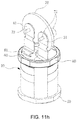
- FIGS. 11A to 11K are perspective views showing a process of assembling the electric double layer device according to the present invention.
- FIG. 12 is a sectional view showing the electric double layer device according to the present invention.
- FIG. 13A is a plan view showing a wound unit that is applied to the electric double layer device according to the present invention.
- FIG. 13B is a half-sectional view showing the wound unit that is applied to the electric double layer device according to the present invention.
- FIG. 13C is a development view showing the wound unit that is applied to the electric double layer device according to the present invention.
- FIG. 13A is a plan view showing a wound applied to an electric double layer device according to the present invention
- FIG. 13B is a half-sectional view showing the wound unit that is applied to the electric double layer device according to the present invention
- FIG. 13C is a development view showing the wound unit that is applied to the electric double layer device according to the present invention.
- a wound unit 10 that is applied to an electric double layer device is configured to have a structure in which a first current collector 11 and a second current collector 12 are wound such that the first current collector 11 extends downward and the second current collector 12 extends upward in a state in which a separator 10 a is disposed between the first current collector 11 and the second current collector 12 .
- the first current collector 11 may be a negative electrode
- the second current collector 12 may be a positive electrode
- the first current collector 11 may be a positive electrode
- the second current collector 12 may be a negative electrode.
- FIG. 10 is an exploded perspective view showing an electric double layer device according to the present invention
- FIGS. 11A to 11K are perspective views showing a process of assembling the electric double layer device according to the present invention
- FIG. 12 is a sectional view showing the electric double layer device according to the present invention.
- the electric double layer device basically includes a wound unit 10 , which includes a first current collector 11 and a second current collector 12 , which are wound while being separated from each other by a separator 10 a , and a case 20 having an upper opening 21 , through which the wound unit 10 is received, and a lower closure 22 .
- the electric double layer device further includes a lower collecting plate 30 connected to the first current collector 11 of the wound unit 10 , the lower collecting plate 30 having a lower terminal 31 extending upward along the outer circumference of the wound unit 10 , a lower insulating plate 50 placed on the lower closure 22 to receive the lower collecting plate 30 , an upper collecting plate 40 connected to the second current collector 12 of the wound unit 10 , the upper collecting plate 40 having an upper terminal 41 extending upward, an upper insulating plate 60 fitted on the upper collecting plate 40 such that the upper terminal 41 and the lower terminal 31 are directed upward, and an upper nonconductive plate 70 fitted in the case 20 to cover the upper opening 21 , the upper nonconductive plate 70 having a first connection terminal 71 and a second connection terminal 72 respectively connected to the lower terminal 31 and the upper terminal 41 .
- the lower terminal 31 is withdrawn from the lower collecting plate 30 , which is connected to the first current collector 11 , and extends upward.
- components such as the connection core and the other terminal, disclosed in Related Art Document 2 are not needed. Consequently, it is possible to omit the process of connecting the connection core to the lower connection plate and the process of connecting the other terminal to toe connection core, which are required in Related Art Document 2, thereby improving productivity and ease of assembly.
- the lower terminal 31 is withdrawn from the lower collecting plate 30 in the same manner as the manner in which the upper terminal 41 is withdrawn from the upper collecting plate 40 , thereby preventing the risk of a poor connection therebetween. In particular, internal equivalent resistance is reduced, and discharge efficiency is improved during the discharge of high current.
- connection terminal 71 and the second connection terminal 72 are more securely positioned by the upper nonconductive plate thereby more smoothly achieving connection with an external apparatus.
- the wound unit 10 for the electric double layer device includes a first current collector 11 and a second current collector 12 , which are wound while being separated from each other by a separator 10 a .
- the lower terminal 31 extends upward along the outer circumference of the wound unit 10 , is bent so as to be placed above the upper insulating plate 60 , and is then bent upward so as to be connected to the first connection terminal 71 .
- the upper insulating plate 60 has therein a through hole 61 through which the upper terminal 41 extends.
- the upper terminal 41 extends upward from the upper collecting plate 40 , extends through the through hole 61 , and is then bent so as to be connected to the second connection terminal 72 .
- the lower terminal 31 and the upper terminal 41 are directly withdrawn respectively from the lower collecting plate 30 and the upper collecting plate 40 without welding, thereby improving productivity and ease of assembly and increasing electrical connection force.
- the upper terminal 41 and the lower terminal 31 may be connected to an external apparatus, such as a cellular phone, a GPS receiver, or an MP3 player.
- the upper terminal 41 and the lower terminal 31 may be connected to a wind energy system, a solar energy system, or a motor of an electric vehicle or a hybrid electric vehicle.
- the electric double layer device further includes an upper insulating ring 80 , disposed so as to be in tight contact with the edge of the upper insulation plate 60 while receiving the lower terminal 31 therein to enable the lower terminal 31 to maintain a state in which the wound unit 10 and the case 20 are spaced apart from each other, thereby more securely insulating the lower terminal 31 .
- the wound unit 10 may be more easily inserted into the case 20 , since the upper insulating ring 80 enables the lower terminal 31 to be disposed in tight contact with the edge of the upper insulation plate 60 .
- the electric double layer device further includes a first through hole 22 a and a second through hole 51 formed respectively through the lower closure 22 of the case 20 and the lower insulating plate 50 so as to be used as introduction ports of an electrolytic solution, a rubber plug 91 fitted in the upper part of the first through hole 22 a to seal the first through hole 22 a , and a closure plug 92 fitted in the lower part of the first through hole 22 a and welded to the lower part of the first through hole 22 a .
- the closure plug 92 may be made of aluminum.
- the electric double layer device according to the present invention may further include curling rubber 93 placed on the edge of the upper nonconductive plate 70 to seal the upper opening 21 after curling of the case 20 , thereby sealing the interior of the case 20 .
- the electric double layer device according to the present invention may further include a beading part 23 provided at the upper part of the case 20 to maximize firmness between the upper nonconductive plate 70 , including the upper terminal 41 and the lower terminal 31 , and the case 20 .
- the lower terminal is directly withdrawn from the lower collecting plate in the same manner as the manner in which the upper terminal is directly withdrawn from the upper collecting plate, thereby improving productivity and ease of assembly, and in addition increasing connection force.
- the lower terminal is directly withdrawn from the lower collecting plate, thereby improving discharge efficiency during the discharge of high current while reducing internal equivalent resistance.
- the electric double layer device further includes an upper insulating ring, configured to enable the lower terminal to maintain a state in which the wound unit and the case are spaced apart from each other, thereby more securely achieving insulation of the lower terminal.
- the upper insulating ring enables the lower terminal to be disposed in tight contact with the edge of the upper insulation plate, whereby the wound unit is more easily inserted into the case.
- an electrolytic solution is introduced into the case via a first through hole and a second through hole in a state in which all parts, including the wound unit, are assembled in the case, thereby improving productivity and workability.
- the present invention may be applied to the field of devices such as a battery, a capacitor, and an electrolytic condenser, which store electrical energy.
Landscapes
- Engineering & Computer Science (AREA)
- Power Engineering (AREA)
- Chemical & Material Sciences (AREA)
- Microelectronics & Electronic Packaging (AREA)
- Chemical Kinetics & Catalysis (AREA)
- Electrochemistry (AREA)
- General Chemical & Material Sciences (AREA)
- Manufacturing & Machinery (AREA)
- Composite Materials (AREA)
- Materials Engineering (AREA)
- Electric Double-Layer Capacitors Or The Like (AREA)
Abstract
Description
Claims (18)
Priority Applications (1)
| Application Number | Priority Date | Filing Date | Title |
|---|---|---|---|
| US14/990,382 US10692662B2 (en) | 2016-01-07 | 2016-01-07 | Electric double layer device |
Applications Claiming Priority (1)
| Application Number | Priority Date | Filing Date | Title |
|---|---|---|---|
| US14/990,382 US10692662B2 (en) | 2016-01-07 | 2016-01-07 | Electric double layer device |
Publications (2)
| Publication Number | Publication Date |
|---|---|
| US20170200567A1 US20170200567A1 (en) | 2017-07-13 |
| US10692662B2 true US10692662B2 (en) | 2020-06-23 |
Family
ID=59275890
Family Applications (1)
| Application Number | Title | Priority Date | Filing Date |
|---|---|---|---|
| US14/990,382 Active 2036-11-20 US10692662B2 (en) | 2016-01-07 | 2016-01-07 | Electric double layer device |
Country Status (1)
| Country | Link |
|---|---|
| US (1) | US10692662B2 (en) |
Families Citing this family (2)
| Publication number | Priority date | Publication date | Assignee | Title |
|---|---|---|---|---|
| KR102616467B1 (en) | 2018-09-27 | 2023-12-21 | 삼성에스디아이 주식회사 | Electrode assembly and secondary battery comprising the same |
| CN116722324A (en) * | 2020-04-09 | 2023-09-08 | 宁德时代新能源科技股份有限公司 | Batteries, battery packs, electrical equipment and methods of manufacturing batteries |
Citations (18)
| Publication number | Priority date | Publication date | Assignee | Title |
|---|---|---|---|---|
| DE2350272A1 (en) * | 1973-10-06 | 1975-04-17 | Bosch Gmbh Robert | Insulating liquid-filled capacitor - has space between wound capacitor and cylindrical housing insulated by liquid |
| JPH11251190A (en) * | 1997-12-22 | 1999-09-17 | Asahi Glass Co Ltd | Electric double layer capacitor |
| KR20000075011A (en) | 1999-05-27 | 2000-12-15 | 권호택 | Connecting Structure of Electric Double Layer Capacitor |
| US20020076604A1 (en) * | 2000-12-20 | 2002-06-20 | Honda Giken Kogyo Kabushiki Kaisha | Charging element device and holding structure therefor |
| US6631072B1 (en) * | 1998-12-05 | 2003-10-07 | Energy Storage Systems Pty Ltd | Charge storage device |
| EP1688975A1 (en) | 2003-11-25 | 2006-08-09 | Asahi Glass Company, Limited | Capacitor |
| US20070105014A1 (en) * | 2005-11-08 | 2007-05-10 | Lg Chem, Ltd. | Electrode assembly prepared in longitudinal folding manner and electrochemical cell employing the same |
| CN201222422Y (en) * | 2008-07-17 | 2009-04-15 | 宁国市大荣电器有限公司 | Built-in inductance explosion-proof capacitor for full automatic washing machine |
| US20100216013A1 (en) * | 2009-02-26 | 2010-08-26 | Dae-Kyu Kim | Cylinder type secondary battery |
| KR20120027665A (en) | 2010-09-13 | 2012-03-22 | 코칩 주식회사 | High-voltage electric double layer capacitor |
| US20120112393A1 (en) * | 2009-07-08 | 2012-05-10 | Captex Co. Ltd | Non-linear spring structure and pressure spacer using the same |
| CN102738498A (en) | 2011-04-04 | 2012-10-17 | Sb锂摩托有限公司 | Secondary battery |
| CN202650836U (en) * | 2012-05-15 | 2013-01-02 | 铜陵市铜新电气有限责任公司 | Insulation sleeve effectively preventing electrical breakdown generated between film capacitor pole-shells |
| CN102959662A (en) | 2010-09-16 | 2013-03-06 | 新神户电机株式会社 | Method for producing electrode plate group unit for lithium-ion capacitor, and lithium-ion capacitor |
| US20130250475A1 (en) * | 2010-11-09 | 2013-09-26 | Nippon Chemi-Con Corporation | Capacitor and method for manufacturing the same |
| CN104103802A (en) | 2013-04-01 | 2014-10-15 | 三星Sdi株式会社 | Rechargeable secondary battery |
| KR20140143641A (en) | 2013-06-07 | 2014-12-17 | 주식회사 네스캡 | Electric double layer device |
| CN105140459A (en) | 2009-12-28 | 2015-12-09 | Jm能源股份有限公司 | Electricity-storage device |
-
2016
- 2016-01-07 US US14/990,382 patent/US10692662B2/en active Active
Patent Citations (19)
| Publication number | Priority date | Publication date | Assignee | Title |
|---|---|---|---|---|
| DE2350272A1 (en) * | 1973-10-06 | 1975-04-17 | Bosch Gmbh Robert | Insulating liquid-filled capacitor - has space between wound capacitor and cylindrical housing insulated by liquid |
| JPH11251190A (en) * | 1997-12-22 | 1999-09-17 | Asahi Glass Co Ltd | Electric double layer capacitor |
| US6631072B1 (en) * | 1998-12-05 | 2003-10-07 | Energy Storage Systems Pty Ltd | Charge storage device |
| KR20000075011A (en) | 1999-05-27 | 2000-12-15 | 권호택 | Connecting Structure of Electric Double Layer Capacitor |
| US20020076604A1 (en) * | 2000-12-20 | 2002-06-20 | Honda Giken Kogyo Kabushiki Kaisha | Charging element device and holding structure therefor |
| EP1688975A1 (en) | 2003-11-25 | 2006-08-09 | Asahi Glass Company, Limited | Capacitor |
| US20060245144A1 (en) * | 2003-11-25 | 2006-11-02 | Asahi Glass Company Limited | Capacitor |
| US20070105014A1 (en) * | 2005-11-08 | 2007-05-10 | Lg Chem, Ltd. | Electrode assembly prepared in longitudinal folding manner and electrochemical cell employing the same |
| CN201222422Y (en) * | 2008-07-17 | 2009-04-15 | 宁国市大荣电器有限公司 | Built-in inductance explosion-proof capacitor for full automatic washing machine |
| US20100216013A1 (en) * | 2009-02-26 | 2010-08-26 | Dae-Kyu Kim | Cylinder type secondary battery |
| US20120112393A1 (en) * | 2009-07-08 | 2012-05-10 | Captex Co. Ltd | Non-linear spring structure and pressure spacer using the same |
| CN105140459A (en) | 2009-12-28 | 2015-12-09 | Jm能源股份有限公司 | Electricity-storage device |
| KR20120027665A (en) | 2010-09-13 | 2012-03-22 | 코칩 주식회사 | High-voltage electric double layer capacitor |
| CN102959662A (en) | 2010-09-16 | 2013-03-06 | 新神户电机株式会社 | Method for producing electrode plate group unit for lithium-ion capacitor, and lithium-ion capacitor |
| US20130250475A1 (en) * | 2010-11-09 | 2013-09-26 | Nippon Chemi-Con Corporation | Capacitor and method for manufacturing the same |
| CN102738498A (en) | 2011-04-04 | 2012-10-17 | Sb锂摩托有限公司 | Secondary battery |
| CN202650836U (en) * | 2012-05-15 | 2013-01-02 | 铜陵市铜新电气有限责任公司 | Insulation sleeve effectively preventing electrical breakdown generated between film capacitor pole-shells |
| CN104103802A (en) | 2013-04-01 | 2014-10-15 | 三星Sdi株式会社 | Rechargeable secondary battery |
| KR20140143641A (en) | 2013-06-07 | 2014-12-17 | 주식회사 네스캡 | Electric double layer device |
Non-Patent Citations (7)
| Title |
|---|
| Decision to Grant dated Jun. 27, 2016 in related Korean Application No. 10-2014-0102566, filed Aug. 8, 2014, in 1 page. |
| Extended European Search Report dated Jul. 1, 2016 in related European Application No. 16152106.7, filed Jan. 20, 2016, in 7 pages. |
| First Office Action dated Jun. 1, 2018 in related Chinese Application No. 201610048460.0. |
| H11-251190 Sep. 1999 English Machine Translation. * |
| H11-251190 Sep. 1999 ESPACENET Abstract. * |
| Notification of Reason for Refusal dated Dec. 4, 2015 in related Korean Application No. 10-2014-0102566, filed Aug. 8, 2014, in 2 pages. |
| Notification of Reason for Refusal dated Jun. 2, 2015 in related Korean Application No. 10-2014-0102566, filed Aug. 8, 2014, in 2 pages. |
Also Published As
| Publication number | Publication date |
|---|---|
| US20170200567A1 (en) | 2017-07-13 |
Similar Documents
| Publication | Publication Date | Title |
|---|---|---|
| KR101537999B1 (en) | Electric double layer device | |
| US6762926B1 (en) | Supercapacitor with high energy density | |
| CN101517817A (en) | Hybrid Electrode Assembly of Capacitor-Battery Structure | |
| US10658128B2 (en) | Electric double-layer device | |
| US10692662B2 (en) | Electric double layer device | |
| KR101599711B1 (en) | Electric double layer device | |
| US20110188171A1 (en) | Electric double layer capacitor and method of manufacturing the same | |
| KR101638566B1 (en) | Electric double layer device | |
| US20110170234A1 (en) | Electric double layer capacitor | |
| KR101732688B1 (en) | Electric double layer device | |
| EP3196906B1 (en) | Electric double layer device | |
| WO2005076296A1 (en) | Electrochemical device and electrode body | |
| EP1471545A1 (en) | Super capacitor with high energy density | |
| CN215451186U (en) | Large-capacity aluminum electrolytic capacitor | |
| KR101999736B1 (en) | An axial-type lithium ion capacitor comprising graphene electrode | |
| HK1242467A (en) | Electric double layer device | |
| HK1242467A1 (en) | Electric double layer device | |
| CN106997809A (en) | Electric double layer device | |
| KR101791894B1 (en) | Electric double layer device | |
| HK1242467B (en) | Electric double layer device | |
| KR100529253B1 (en) | Supercapacitor with high energy density | |
| CN215451185U (en) | Aluminum electrolytic capacitor cover plate and aluminum electrolytic capacitor | |
| KR101211667B1 (en) | Super capacitor type of pouch and manufacturing method | |
| KR101258545B1 (en) | Electric energy storage device improved in resistance-characteristics, fabrication method thereof and inner terminal structure for the same | |
| KR101900179B1 (en) | Apparatus for manufacturing electrochemical double layer cell |
Legal Events
| Date | Code | Title | Description |
|---|---|---|---|
| AS | Assignment |
Owner name: NESSCAP CO., LTD, KOREA, REPUBLIC OF Free format text: ASSIGNMENT OF ASSIGNORS INTEREST;ASSIGNORS:KIM, YOUNG JIN;JUNG, GWAN GOO;REEL/FRAME:037547/0040 Effective date: 20160113 |
|
| STCV | Information on status: appeal procedure |
Free format text: APPEAL BRIEF (OR SUPPLEMENTAL BRIEF) ENTERED AND FORWARDED TO EXAMINER |
|
| STPP | Information on status: patent application and granting procedure in general |
Free format text: NON FINAL ACTION MAILED |
|
| STPP | Information on status: patent application and granting procedure in general |
Free format text: RESPONSE TO NON-FINAL OFFICE ACTION ENTERED AND FORWARDED TO EXAMINER |
|
| STPP | Information on status: patent application and granting procedure in general |
Free format text: PUBLICATIONS -- ISSUE FEE PAYMENT VERIFIED |
|
| STCF | Information on status: patent grant |
Free format text: PATENTED CASE |
|
| AS | Assignment |
Owner name: MAXWELL TECHNOLOGIES KOREA CO., LTD., KOREA, REPUBLIC OF Free format text: CHANGE OF NAME;ASSIGNOR:NESSCAP CO., LTD.;REEL/FRAME:053636/0967 Effective date: 20190102 |
|
| CC | Certificate of correction | ||
| FEPP | Fee payment procedure |
Free format text: ENTITY STATUS SET TO SMALL (ORIGINAL EVENT CODE: SMAL); ENTITY STATUS OF PATENT OWNER: SMALL ENTITY |
|
| MAFP | Maintenance fee payment |
Free format text: PAYMENT OF MAINTENANCE FEE, 4TH YR, SMALL ENTITY (ORIGINAL EVENT CODE: M2551); ENTITY STATUS OF PATENT OWNER: SMALL ENTITY Year of fee payment: 4 |