US10692563B2 - Semiconductor memory device and memory system - Google Patents
Semiconductor memory device and memory system Download PDFInfo
- Publication number
- US10692563B2 US10692563B2 US15/695,866 US201715695866A US10692563B2 US 10692563 B2 US10692563 B2 US 10692563B2 US 201715695866 A US201715695866 A US 201715695866A US 10692563 B2 US10692563 B2 US 10692563B2
- Authority
- US
- United States
- Prior art keywords
- semiconductor memory
- controller
- read
- memory device
- voltage
- Prior art date
- Legal status (The legal status is an assumption and is not a legal conclusion. Google has not performed a legal analysis and makes no representation as to the accuracy of the status listed.)
- Active, expires
Links
Images


Classifications
-
- G—PHYSICS
- G11—INFORMATION STORAGE
- G11C—STATIC STORES
- G11C11/00—Digital stores characterised by the use of particular electric or magnetic storage elements; Storage elements therefor
- G11C11/21—Digital stores characterised by the use of particular electric or magnetic storage elements; Storage elements therefor using electric elements
- G11C11/34—Digital stores characterised by the use of particular electric or magnetic storage elements; Storage elements therefor using electric elements using semiconductor devices
- G11C11/40—Digital stores characterised by the use of particular electric or magnetic storage elements; Storage elements therefor using electric elements using semiconductor devices using transistors
- G11C11/401—Digital stores characterised by the use of particular electric or magnetic storage elements; Storage elements therefor using electric elements using semiconductor devices using transistors forming cells needing refreshing or charge regeneration, i.e. dynamic cells
- G11C11/4063—Auxiliary circuits, e.g. for addressing, decoding, driving, writing, sensing or timing
- G11C11/407—Auxiliary circuits, e.g. for addressing, decoding, driving, writing, sensing or timing for memory cells of the field-effect type
- G11C11/408—Address circuits
- G11C11/4085—Word line control circuits, e.g. word line drivers, - boosters, - pull-up, - pull-down, - precharge
-
- G—PHYSICS
- G11—INFORMATION STORAGE
- G11C—STATIC STORES
- G11C7/00—Arrangements for writing information into, or reading information out from, a digital store
- G11C7/04—Arrangements for writing information into, or reading information out from, a digital store with means for avoiding disturbances due to temperature effects
-
- G—PHYSICS
- G11—INFORMATION STORAGE
- G11C—STATIC STORES
- G11C11/00—Digital stores characterised by the use of particular electric or magnetic storage elements; Storage elements therefor
- G11C11/21—Digital stores characterised by the use of particular electric or magnetic storage elements; Storage elements therefor using electric elements
- G11C11/34—Digital stores characterised by the use of particular electric or magnetic storage elements; Storage elements therefor using electric elements using semiconductor devices
- G11C11/40—Digital stores characterised by the use of particular electric or magnetic storage elements; Storage elements therefor using electric elements using semiconductor devices using transistors
- G11C11/401—Digital stores characterised by the use of particular electric or magnetic storage elements; Storage elements therefor using electric elements using semiconductor devices using transistors forming cells needing refreshing or charge regeneration, i.e. dynamic cells
- G11C11/406—Management or control of the refreshing or charge-regeneration cycles
- G11C11/40626—Temperature related aspects of refresh operations
-
- G—PHYSICS
- G11—INFORMATION STORAGE
- G11C—STATIC STORES
- G11C11/00—Digital stores characterised by the use of particular electric or magnetic storage elements; Storage elements therefor
- G11C11/21—Digital stores characterised by the use of particular electric or magnetic storage elements; Storage elements therefor using electric elements
- G11C11/34—Digital stores characterised by the use of particular electric or magnetic storage elements; Storage elements therefor using electric elements using semiconductor devices
- G11C11/40—Digital stores characterised by the use of particular electric or magnetic storage elements; Storage elements therefor using electric elements using semiconductor devices using transistors
- G11C11/401—Digital stores characterised by the use of particular electric or magnetic storage elements; Storage elements therefor using electric elements using semiconductor devices using transistors forming cells needing refreshing or charge regeneration, i.e. dynamic cells
- G11C11/4063—Auxiliary circuits, e.g. for addressing, decoding, driving, writing, sensing or timing
- G11C11/407—Auxiliary circuits, e.g. for addressing, decoding, driving, writing, sensing or timing for memory cells of the field-effect type
- G11C11/4074—Power supply or voltage generation circuits, e.g. bias voltage generators, substrate voltage generators, back-up power, power control circuits
-
- G—PHYSICS
- G11—INFORMATION STORAGE
- G11C—STATIC STORES
- G11C11/00—Digital stores characterised by the use of particular electric or magnetic storage elements; Storage elements therefor
- G11C11/21—Digital stores characterised by the use of particular electric or magnetic storage elements; Storage elements therefor using electric elements
- G11C11/34—Digital stores characterised by the use of particular electric or magnetic storage elements; Storage elements therefor using electric elements using semiconductor devices
- G11C11/40—Digital stores characterised by the use of particular electric or magnetic storage elements; Storage elements therefor using electric elements using semiconductor devices using transistors
- G11C11/401—Digital stores characterised by the use of particular electric or magnetic storage elements; Storage elements therefor using electric elements using semiconductor devices using transistors forming cells needing refreshing or charge regeneration, i.e. dynamic cells
- G11C11/4063—Auxiliary circuits, e.g. for addressing, decoding, driving, writing, sensing or timing
- G11C11/407—Auxiliary circuits, e.g. for addressing, decoding, driving, writing, sensing or timing for memory cells of the field-effect type
- G11C11/409—Read-write [R-W] circuits
- G11C11/4091—Sense or sense/refresh amplifiers, or associated sense circuitry, e.g. for coupled bit-line precharging, equalising or isolating
-
- G—PHYSICS
- G11—INFORMATION STORAGE
- G11C—STATIC STORES
- G11C11/00—Digital stores characterised by the use of particular electric or magnetic storage elements; Storage elements therefor
- G11C11/21—Digital stores characterised by the use of particular electric or magnetic storage elements; Storage elements therefor using electric elements
- G11C11/34—Digital stores characterised by the use of particular electric or magnetic storage elements; Storage elements therefor using electric elements using semiconductor devices
- G11C11/40—Digital stores characterised by the use of particular electric or magnetic storage elements; Storage elements therefor using electric elements using semiconductor devices using transistors
- G11C11/401—Digital stores characterised by the use of particular electric or magnetic storage elements; Storage elements therefor using electric elements using semiconductor devices using transistors forming cells needing refreshing or charge regeneration, i.e. dynamic cells
- G11C11/4063—Auxiliary circuits, e.g. for addressing, decoding, driving, writing, sensing or timing
- G11C11/407—Auxiliary circuits, e.g. for addressing, decoding, driving, writing, sensing or timing for memory cells of the field-effect type
- G11C11/409—Read-write [R-W] circuits
- G11C11/4099—Dummy cell treatment; Reference voltage generators
-
- G—PHYSICS
- G11—INFORMATION STORAGE
- G11C—STATIC STORES
- G11C11/00—Digital stores characterised by the use of particular electric or magnetic storage elements; Storage elements therefor
- G11C11/56—Digital stores characterised by the use of particular electric or magnetic storage elements; Storage elements therefor using storage elements with more than two stable states represented by steps, e.g. of voltage, current, phase, frequency
- G11C11/5621—Digital stores characterised by the use of particular electric or magnetic storage elements; Storage elements therefor using storage elements with more than two stable states represented by steps, e.g. of voltage, current, phase, frequency using charge storage in a floating gate
- G11C11/5642—Sensing or reading circuits; Data output circuits
-
- G—PHYSICS
- G11—INFORMATION STORAGE
- G11C—STATIC STORES
- G11C16/00—Erasable programmable read-only memories
- G11C16/02—Erasable programmable read-only memories electrically programmable
- G11C16/04—Erasable programmable read-only memories electrically programmable using variable threshold transistors, e.g. FAMOS
- G11C16/0483—Erasable programmable read-only memories electrically programmable using variable threshold transistors, e.g. FAMOS comprising cells having several storage transistors connected in series
-
- G—PHYSICS
- G11—INFORMATION STORAGE
- G11C—STATIC STORES
- G11C16/00—Erasable programmable read-only memories
- G11C16/02—Erasable programmable read-only memories electrically programmable
- G11C16/06—Auxiliary circuits, e.g. for writing into memory
- G11C16/26—Sensing or reading circuits; Data output circuits
-
- G—PHYSICS
- G11—INFORMATION STORAGE
- G11C—STATIC STORES
- G11C7/00—Arrangements for writing information into, or reading information out from, a digital store
- G11C7/06—Sense amplifiers; Associated circuits, e.g. timing or triggering circuits
- G11C7/08—Control thereof
-
- G—PHYSICS
- G11—INFORMATION STORAGE
- G11C—STATIC STORES
- G11C8/00—Arrangements for selecting an address in a digital store
- G11C8/08—Word line control circuits, e.g. drivers, boosters, pull-up circuits, pull-down circuits, precharging circuits, for word lines
-
- G—PHYSICS
- G11—INFORMATION STORAGE
- G11C—STATIC STORES
- G11C7/00—Arrangements for writing information into, or reading information out from, a digital store
- G11C7/14—Dummy cell management; Sense reference voltage generators
Definitions
- One or more embodiments described herein relate generally to a semiconductor memory device and a memory system.
- Some memory systems include a negative-AND (NAND) type flash memory as a semiconductor memory device and a controller that controls the NAND type flash memory.
- NAND negative-AND
- FIG. 1 is a block diagram for describing the configuration of one or more embodiments of a memory system according to a first aspect.
- FIG. 2 is a block diagram for describing the configuration of one or more embodiments of a semiconductor memory device according to the first aspect.
- FIG. 3 is a circuit diagram for describing the configuration of a memory cell array of one or more embodiments of the semiconductor memory device according to the first aspect.
- FIG. 4 is a cross-sectional view for describing the configuration of the memory cell array of one or more embodiments of the semiconductor memory device according to the first aspect.
- FIG. 5 is a schematic view for describing a threshold voltage distribution of a memory cell transistor of one or more embodiments of the semiconductor memory device according to the first aspect.
- FIG. 6 is a table for describing example temperature compensation values applied during operation of the semiconductor memory device according to the first aspect.
- FIG. 7 is a command sequence for describing one or more embodiments of a lock/unlock operation of the semiconductor memory device according to the first aspect.
- FIG. 8 is a flowchart for describing one or more embodiments of an operation of the memory system according to the first aspect.
- FIGS. 9A and 9B are schematic views for describing a variation in threshold voltage distribution of one or more embodiments of the semiconductor memory device according to the first aspect.
- FIG. 10A , FIG. 10B and FIG. 10C are schematic views for describing an outline of one or more embodiments of a Vth tracking operation of the semiconductor memory device according to the first aspect.
- FIG. 11 is a flowchart for describing one or more embodiments of the Vth tracking operation of the memory system according to the first aspect.
- FIG. 12 is a command sequence for describing one or more embodiments of a single level reading operation of the semiconductor memory device according to the first aspect.
- FIG. 13 is a schematic view for describing one or more embodiments of an outline of a soft bit reading operation of the semiconductor memory device according to the first aspect.
- FIG. 14 is a flowchart for describing one or more embodiments of the soft bit reading operation of the memory system according to the first aspect.
- FIG. 15 is a table for describing one or more embodiments of the soft bit reading operation of the semiconductor memory device according to the first aspect.
- FIG. 16 is a command sequence for describing one or more embodiments of a shift reading operation of the semiconductor memory device according to the first aspect.
- FIG. 17 is a schematic view for describing an outline of an operation of the semiconductor memory device according to a comparative example.
- One or more embodiments described herein provide for suppressing deterioration in data reading accuracy of a memory device.
- One or more embodiments of a semiconductor memory device include a memory cell transistor, a word line coupled to the memory cell transistor, a temperature detecting element configured to detect a temperature, and a control unit.
- the control unit is configured to determine, responsive to receiving a first command from a controller, a compensation value for a read voltage designated by the controller according to the detected temperature, and to lock updating of the compensation value.
- One or more embodiments of a method for performing a read operation include determining, by a controller, that a read error has occurred, and implementing, by the controller, a tracking operation. The method further includes determining, by the controller, a standard read value based on the tracking operation, and performing, by the controller, a read operation using the standard read value.
- a common reference numeral may be given to components having the same or similar functions and configurations. Further, when plural components having a common reference numeral are distinguished from each other, subscripts may be added to the common reference numeral so as to distinguish the components. In addition, in the case where the plural components need not particularly be distinguished from each other, the subscript may be omitted.
- FIG. 1 is a block diagram illustrating one example of a configuration of a memory system according to a first aspect.
- the memory system 1 communicates with, for example, an external host device (not illustrated).
- the memory system 1 stores data from the host device (not illustrated) and further, reads the data to the host device.
- the memory system 1 includes a controller 10 and a semiconductor memory device (e.g. a NAND flash memory) 20 .
- the controller 10 receives a command from the host device and controls the semiconductor memory device 20 based on the received command.
- the controller 10 writes the data instructed to be written from the host device to the semiconductor memory device 20 , and the controller 10 reads the data instructed to be read from the semiconductor memory device 20 and transmits the read data to the host device.
- the controller 10 is electrically connected to the semiconductor memory device 20 by a NAND bus, for example.
- the semiconductor memory device 20 includes plural memory cells and stores data in a nonvolatile manner.
- the NAND bus transmits and receives signals such as “CE,” “CLE,” “ALE,” “/WE,” “/RE,” “/WP,” “/RB,” and “I/O ⁇ 7:0>” according to a NAND interface via individual signal lines, respectively.
- the signal /CE is a signal for enabling the semiconductor memory device 20 .
- the signal CLE notifies the semiconductor memory device 20 that the signal I/O ⁇ 7:0> which flows in the semiconductor memory device 20 while the signal CLE is at a “high (H)” level is a command.
- the signal ALE notifies the semiconductor memory device 20 that the signal I/O ⁇ 7:0> which flows in the semiconductor memory device 20 while the signal ALE is at the “H” level is an address.
- the signal /WE instructs the semiconductor memory device 20 to take in the signal I/O ⁇ 7:0> which flows in the semiconductor memory device 20 while the signal /WE is at a “low (L)” level.
- the signal /RE instructs the semiconductor memory device 20 to output the signal I/O ⁇ 7:0>.
- the signal /WP instructs the semiconductor memory device 20 to prevent data from being written and erased.
- the signal /RB indicates whether the semiconductor memory device 20 is in a ready state (a state of being able to receive a command from an external device) or a busy state (a state of not being able to receive a command from an external device).
- the signal I/O ⁇ 7:0> is, for example, an 8-bit signal.
- the signal I/O ⁇ 7:0> is, for example, at least a portion of data transmitted and received between the semiconductor memory device 20 and the controller 10 and includes a command CMD, an address ADD, and data DAT.
- the data DAT includes write data and read data.
- the controller 10 includes a processor (central processing unit (CPU)) 11 , a memory (random access memory (RAM)) 12 , an error check and correction (ECC) circuit 13 , a NAND interface circuit 14 , a buffer memory 15 , and a host interface circuit 16 .
- CPU central processing unit
- RAM random access memory
- ECC error check and correction
- the processor 11 controls the overall operation of the controller 10 .
- the processor 11 issues a read command based on the NAND interface to the semiconductor memory device 20 , for example, in response to a read command of the data received from the host device. Such an operation is similarly applied to cases of writing and erasing. Further, the processor 11 has a function of executing various operations on the read data from the semiconductor memory device 20 .
- the memory 12 is a semiconductor memory such as a static RAM (SRAM) or a dynamic RAM (DRAM), and is used as a work area of the processor 11 .
- the memory 12 stores firmware and various management tables for managing the semiconductor memory device 20 .
- the memory 12 may be embedded in the controller 10 or mounted external to the controller 10 .
- the ECC circuit 13 performs error detection and error correction processing of the data stored in the semiconductor memory device 20 . That is, when data is written, the ECC circuit 13 generates an error correction code and assigns the generated error correction code to the written data. Further, when data is read, the ECC circuit 13 decodes the data based on the ECC code and detects the presence or absence of an error. In addition, when an error is detected, the ECC circuit 13 specifies a bit position of the error and corrects the error.
- An error correction method includes, for example, hard bit decoding and soft bit decoding.
- Bose-Chaudhuri-Hocquenghem (BCH) code or a Reed-Solomon (RS) code may be used as a hard bit decoding code used for the hard bit decoding, and for example, a low density parity check (LDPC) code or the like may be used as a soft bit decoding code used for the soft bit decoding.
- BCH Bose-Chaudhuri-Hocquenghem
- RS Reed-Solomon
- the NAND interface circuit 14 is electrically connected to the semiconductor memory device 20 via the NAND bus to manage communication with the semiconductor memory device 20 .
- the NAND interface circuit 14 transmits the command CMD, the address ADD, and the write data DAT to the semiconductor memory device 20 according to the instruction of the processor 11 . Further, the NAND interface circuit 14 receives the read data DAT from the semiconductor memory device 20 .
- the buffer memory 15 temporarily holds data and the like that the controller 10 receives from the semiconductor memory device 20 and the host device.
- the buffer memory 15 is also used as, for example, a memory area for temporarily holding the read data from the semiconductor memory device 20 and an operation result for the read data.
- the host interface circuit 16 is electrically connected to the host device to manage communication with the host device.
- the host interface circuit 16 transmits, for example, the command and the data received from the host device to the processor 11 and the buffer memory 15 , respectively.
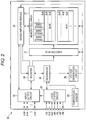
- FIG. 2 is a block diagram illustrating an example of a configuration of a semiconductor memory device according to the first aspect.
- the semiconductor memory device 20 includes a memory cell array 21 , an input/output circuit 22 , a logic control circuit 23 , a register 24 , a sequencer 25 , a voltage generation circuit 26 , a row decoder 27 , a sense amplifier module 28 , and a temperature sensor 29 .
- the memory cell array 21 includes plural blocks BLK (BLK 0 , BLK 1 , . . . ).
- the blocks BLK include plural non-volatile memory cell transistors (not illustrated) associated with word lines and bit lines.
- a block BLK is, for example, an erase unit of data, and the data in the same block BLK is collectively erased.
- Each block BLK includes plural string units SU (SU 0 , SU 1 , SU 2 , . . . ).
- Each string unit SU is a set of NAND strings NS.
- the NAND string NS includes plural memory cell transistors. Further, the number of blocks in the memory cell array 21 , the number of string units in one block BLK, and the number of NAND strings in one string unit SU may be arbitrarily set.
- the input/output circuit 22 transmits or receives signals I/O (I/O 0 to I/O 7 ) to or from the controller 10 .
- the input/output circuit 22 transmits commands CMD and addresses ADD in the signals I/O to the register 24 .
- the input/output circuit 22 transmits or receives the write data and the read data to or from the sense amplifier module 28 .
- the logic control circuit 23 receives the signals /CE, CLE, ALE, /WE, /RE, and /WP from the controller 10 . Further, the logic control circuit 23 transmits the signal /RB to the controller 10 so as to notify an external device of a state of the semiconductor memory device 20 .
- the register 24 holds the command CMD and the address ADD.
- the register 24 transmits the addresses ADD to the row decoder 27 and the sense amplifier module 28 , and transmits the commands CMD to the sequencer 25 .
- the sequencer 25 receives the commands CMD, and controls the entire semiconductor memory device 20 according to a sequence based on the received commands CMD. Further, the sequencer 25 receives temperature information from the temperature sensor 29 . The sequencer 25 determines, for example, a value of a voltage to be generated during operations such as writing and reading of data, based on the command CMD and the temperature information.
- the voltage generation circuit 26 generates a voltage required for the operations such as writing, reading, and erasing of data based on an instruction from the sequencer 25 .
- the voltage generation circuit 26 includes a driver that supplies the generated voltage to the row decoder 27 and the sense amplifier module 28 .
- the row decoder 27 receives a row address among the addresses ADD from the register 24 and selects the block BLK based on the row address. In addition, the voltage from the voltage generation circuit 26 is transmitted to the selected block BLK via the row decoder 27 .
- the sense amplifier module 28 When data is read, the sense amplifier module 28 senses the read data read from the memory cell transistor to the bit line, and transmits the sensed read data to the input/output circuit 22 . When data is written, the sense amplifier module 28 transmits write data written through the bit line to the memory cell transistor. Further, the sense amplifier module 28 receives a column address among the addresses ADD from the register 24 and outputs data of a column based on the column address.
- the temperature sensor 29 includes a temperature detection element that detects the temperature of the semiconductor memory device 20 .
- the temperature sensor 29 generates, for example, temperature information corresponding to the temperature detected by the temperature detection element, and transmits the generated temperate information to the sequencer 25 .
- the temperature information is used, for example, for correcting the voltage generated by the voltage generating circuit 26 in the writing operation or the reading operation.
- the temperature information may be information indicating the temperature or a change in temperature, information indicating a voltage value or a change in voltage value, or information generated from the information indicating the temperature and intermediate information used for determining the voltage value.
- FIG. 3 illustrates an example of a circuit diagram for describing the configuration of the memory cell array of one or more embodiments of the semiconductor memory device according to the first aspect.
- each of the NAND strings NS includes, for example, eight memory cell transistors MT: MT 0 , MT 1 , MT 2 , MT 3 , MT 4 , MT 5 , MT 6 , MT 7 (MT 0 to MT 7 ), a selection transistor ST 1 , and a selection transistor ST 2 .
- the number of memory cell transistors MT is not limited to eight, and may be 16, 32, 64, 128, for example, but is not limited to these numbers.
- a memory cell transistor MT includes a stacked gate including a control gate and a charge storage layer. Each memory cell transistor MT is electrically connected in series between the selection transistors ST 1 and ST 2 .
- the term. “electrically connected” is used to refer to configurations in which two conductive components are in contact with each other, as well as configurations in which another conductive component is interposed between the two conductive components.
- the gates of the selection transistors ST 1 of the string units SU 0 , SU 1 , SU 2 , and SU 3 are electrically connected to selection gate lines SGD 0 , SGD 1 , SGD 2 , and SGD 3 (SGD 0 to SGD 3 ), respectively. Further, the gates of the selection transistors ST 2 of all the string units SU in the block BLK are commonly electrically connected to a selection gate line SGS.
- the control gates of the memory cell transistors MT 0 to MT 7 in the same block BLK are electrically connected to the word lines WL 0 , WL 1 , WL 2 , WL 3 , WL 4 , WL 5 , WL 6 , WL 7 (WL 0 to WL 7 ), respectively. That is, word lines WL having the same address are commonly electrically connected to the string units SU in the same block BLK (e.g. all of the string units SU in the same block BLK), and the selection gate line SGS is commonly electrically connected to the string units SU in the same block BLK (e.g. all of the string units SU in the same block BLK). Meanwhile, the selection gate lines SGD are electrically connected to one of the string units SU (e.g. only one of the string units SU) in the same block BLK.
- the other end of the selection transistor ST 1 of the NAND string NS in the same row is electrically connected to any of the m bit lines BL (BL 0 to BL (m ⁇ 1) (m is a natural number of 2 or more)).
- the bit lines BL are commonly electrically connected to the NAND strings NS of the same column across the plural blocks BLK.
- the other end of the selection transistor ST 2 is electrically connected to a source line CELSRC.
- the source line CELSRC is commonly electrically connected to the plural NAND strings NS across the plural blocks BLK.
- data erasing is collectively performed for the memory cell transistors MT in the same block BLK, for example.
- data reading and data writing may be collectively performed for the plural memory cell transistors MT commonly electrically connected to any one word line WL in any one string unit SU of any one block BLK.
- a set of memory cell transistors MT sharing the word line WL in one string unit SU is referred to as, for example, a cell unit CU. That is, the cell unit CU is a set of memory cell transistors MT in which writing or reading operation is collectively performed.
- the cell unit CU includes, for example, one or plural sets of memory areas, and the writing or reading operation for one cell unit CU is executed for one set of memory areas.
- a unit of such a memory area is referred to as a ‘page’.
- FIG. 4 illustrates an example of a cross-sectional structure of a part of the memory cell array of the semiconductor memory device according to the first aspect.
- FIG. 4 illustrates two NAND strings NS of each of two string units SU in one block BLK and peripheral parts thereof.
- the configuration of NAND strings NS illustrated in FIG. 4 is arranged in a plural number in an X direction (in accordance with the coordinate system shown in FIG. 4 ), and for example, the set of plural NAND strings NS aligned along the X direction corresponds to one string unit SU.
- the semiconductor memory device 20 is provided on a semiconductor substrate 30 .
- a plane parallel to the surface of the semiconductor substrate 30 is defined as an XY plane, and a direction orthogonal to the XY plane is defined as a Z direction. Further, the X direction and the Y direction are assumed to be orthogonal to each other.
- a p-type well region 30 p is formed on the top of the semiconductor substrate 30 .
- the plural NAND strings NS are installed on the p-type well region 30 p . That is, on the p-type well region 30 p , for example, a wiring layer 31 serving as the selection gate line SGS, eight wiring layers 32 (WL 0 to WL 7 ) serving as word lines WL 0 to WL 7 , and a wiring layer 33 serving as the selection gate line SGD are sequentially stacked.
- the wiring layer 31 and the wiring layer 33 may be stacked in a plural number.
- An insulating film (not illustrated) is provided between each two adjacent stacked wiring layers 31 to 33 .
- the wiring layer 31 is commonly electrically connected to the gates of the respective selection transistors ST 2 of the plural NAND strings NS in one block BLK, for example.
- the wiring layers 32 are commonly electrically connected to control gates of the respective memory cell transistors MT of the plural NAND strings NS in one block BLK for each layer.
- the wiring layer 33 is commonly electrically connected to the gates of the respective selection transistors ST 1 of the plural NAND strings NS in one string unit SU.
- a memory hole MH is formed to pass through the wiring layers 33 , 32 , and 31 and reach the p-type well region 30 p .
- a block insulating film 34 On a side surface of the memory hole MH (a surface defining the memory hole MH), a block insulating film 34 , a charge storage layer (insulating film) 35 , and a tunnel oxide film 36 are sequentially provided.
- a semiconductor pillar (conductive film) 37 is buried in, or disposed in, the memory hole MH.
- the semiconductor pillar 37 is, for example, non-doped polysilicon and serves as a current path for the NAND string NS.
- a wiring layer 38 serving as a bit line BL is provided on the upper end of the semiconductor pillar 37 .
- the selection transistor ST 2 , the plural memory cell transistors MT, and the selection transistor ST 1 are sequentially stacked above the p-type well region 30 p , and one memory hole MH corresponds to one NAND string NS.
- An n + -type impurity diffusion region 39 and a p + -type impurity diffusion region 40 are provided in the upper portion of the p-type well region 30 p .
- a contact plug 41 is provided on the upper surface of the n + -type impurity diffusion region 39 .
- a wiring layer 42 serving as the source line CELSRC is provided on the upper surface of the contact plug 41 .
- a contact plug 43 is provided on the upper surface of the p + -type impurity diffusion region 40 .
- a wiring layer 44 serving as a well line CPWELL is provided on the upper surface of the contact plug 43 .
- the memory cell array 21 may have other configurations.
- a configuration of the memory cell array 21 is disclosed in, for example, U.S. patent application Ser. No. 12/407,403 entitled “Three-dimensional stacked non-volatile semiconductor memory” and filed on Mar. 19, 2009. Further, other configurations of the memory cell array 21 are disclosed in U.S. patent application Ser. No. 12/406,524, entitled “Three-Dimensional Stacked Non-volatile Semiconductor Memory” and filed on Mar. 18, 2009, U.S. patent application Ser. No. 12/679,991 entitled “Nonvolatile Semiconductor Memory Device and Manufacturing Method Thereof” and filed on Mar. 25, 2010, and U.S. patent application Ser. No. 12/532,030 entitled “Semiconductor Memory and Method of Manufacturing The Same” and filed on Mar. 23, 2009. These patent applications are incorporated herein by reference in their entireties.
- FIG. 5 is a schematic view for describing an example of a threshold voltage distribution of a memory cell transistor of the semiconductor memory device according to the first aspect.
- FIG. 5 an example of a case where 3-bit data is stored in one memory cell transistor MT (triple level cell (TLC)) is illustrated.
- TLC triple level cell
- the threshold voltage of a memory cell transistor MT may hold 3-bit data based on an upper bit (upper data), a middle bit (middle data), and a lower bit (lower data), that is, “111”, “110”, “100”, “000”, “010”, “011”, “001”, or “101” data.
- the threshold voltage distribution of the “111” data is at an “Er” level, which corresponds to, for example, a data erase state.
- the threshold voltages included in the “Er” level is smaller than a read voltage AR and has a positive or negative value.
- the threshold voltage distributions of “110”, “100”, “000”, “010”, “011”, “001”, and “101” data are at “A”, “B”, “C”, “D”, “E”, “F”, and “G” levels, respectively.
- the “A” level to “G” level correspond to a state where charges are injected into the charge storage layer 35 and data is written in the memory cell transistor MT, and the threshold voltage included in each distribution has, for example, a positive value.
- the threshold voltages included in the “A” level are larger than the read voltage AR and further, smaller than a read voltage BR.
- the threshold voltages included in the “B” level are larger than the read voltage BR and further, smaller than read voltage CR.
- the threshold voltages included in the “C” level are larger than the read voltage CR and further, smaller than read voltage DR.
- the threshold voltages included in the “D” level are larger than the read voltage DR and further, smaller than read voltage ER.
- the threshold voltages included in the “E” level are larger than the read voltage ER and further, smaller than read voltage FR.
- the threshold voltages included in the “F” level are larger than the read voltage FR and further, smaller than read voltage GR.
- the threshold voltages included in the “G” level are larger than the read voltage GR and further, smaller than voltage VREAD.
- the voltage VREAD is a voltage applied to a word line WL that is not a reading target when data is written in a certain block BLK.
- each memory cell transistor MT may be in any one of eight threshold voltage distributions, so that each memory cell transistor MT may assume any of eight states. Further, a relationship between each piece of data and a threshold level is not limited to the above relationships, but may be appropriately changed.
- data writing and data reading are performed in units of pages in one cell unit CU.
- the data is written and read for every lower bit, every middle bit, or every upper bit. Therefore, when a memory cell transistor MT holds 3-bit data, data corresponding to the upper bit, the middle bit, and the lower bit are respectively allocated to three pages in one cell unit CU.
- pages that are collectively written or read for the upper bit, the middle bit, and the lower bit will be referred to as an upper page, a middle page, and a lower page, respectively.
- the aforementioned read voltages AR to GR are each determined by a respective “standard value” and a respective “compensation value” that may be aggregated with the standard value to determine each of the read voltages AR to GR.
- the standard value is appropriately determined according to, for example, a reading method.
- the reading method includes, for example, normal reading, shift reading, and single level reading.
- the normal reading is a basic reading method and the read voltage in the normal reading can serve as the reference of the read voltage of the shift reading.
- a shift amount for the standard value is set based on the standard value of the read voltage in the normal reading.
- the standard value of independent read voltage may be set apart from the normal reading.
- the compensation value a value determined based on various parameters may be applied.
- the compensation value may be an aggregation of values including, for example, a temperature compensation value determined based on the temperature.
- FIG. 6 illustrates an example of a table for describing a temperature compensation value of read voltage of the semiconductor memory device according to the first aspect.
- the sequencer 25 applies a temperature compensation value dV to the standard value to set the read voltages AR to GR according to the temperature in the semiconductor memory device 20 when the reading operation is executed.
- the temperature T is, for example, a temperature detected by the temperature sensor 29 .
- the temperature T may be calculated based on the temperature detected by the temperature sensor 29 , for example.
- the temperature compensation value dV to be applied may correspond to the temperature T as shown in the table shown in FIG. 6 .
- the temperature compensation value dV is set to 0 V. That is, the read voltages AR to GR are not corrected from the standard value.
- the temperature compensation value dV is set to about 0.05 V. That is, the read voltages AR to GR are corrected to be a value larger than the standard value by about +0.05 V.
- the temperature T is 35° C. or more and less than 60° C.
- the temperature compensation value dV is set to about 0.10 V. That is, the read voltages AR to GR are corrected to be a value larger than the standard value by about +0.10 V.
- the temperature compensation value dV is set to about 0.15 V. That is, the read voltages AR to GR are corrected to be a value larger than the standard value by about +0.15 V.
- the sequencer 25 may allow the voltage generation circuit 26 to generate optimum read voltages AR to GR while considering an influence of a characteristic of the memory cell transistor MT which varies according to the temperature when data is read.
- the temperature compensation value dV is not limited to those shown in FIG. 6 , and a value (e.g. a predetermined value) may be set according to the temperature.
- FIG. 6 illustrates a case where the temperature compensation value dV is determined based only on the temperature T is described, but the embodiments disclosed herein are not limited thereto.
- the temperature compensation value dV may be determined based on the temperature T and parameters other than the temperature T.
- the temperature compensation value dV may be applied to all of the read voltages AR to GR or only to some of the read voltages AR to GR.
- a common temperature compensation value dV may be applied to a set of the read voltages AR to GR (e.g. to each of the read voltages AR to GR), or different temperature compensation values dV may be applied to the respective read voltages AR to GR.
- the temperature compensation value dV for the voltage applied in the reading operation is described, but is not limited thereto.
- the sequencer 25 may apply the temperature compensation value dV based on the temperature T to the voltage applied not only in the reading operation but also in the writing operation. Further, the temperature compensation value dV applied in the writing operation may be different from that applied in the reading operation.
- the lock/unlock operation is an operation related to a function of correcting a voltage applied to a word line WL during the writing operation or reading operation in the semiconductor memory device 20 .
- the lock/unlock operation includes a lock operation and an unlock operation.
- the temperature compensation value dV determined in the lock operation and to be applied in the operation after the lock operation is fixed irrespective of the variation of the value of the temperature T after the lock operation.
- the temperature compensation value dV determined in the unlock operation and to be applied in the operation after the unlock operation is determined according to the variation of the value of the temperature T after the unlock operation.
- the unlock operation may resume updating of the temperature compensation value dV locked by the lock operation.
- FIG. 7 is an example command sequence for describing the lock/unlock operation of the semiconductor memory device according to the first aspect.
- the controller 10 instructs the semiconductor memory device 20 to perform a lock non-target operation.
- the sequencer 25 receives the temperature information corresponding to the temperature T from the temperature sensor 29 . Based on the temperature information, the sequencer 25 determines a temperature compensation value dV 1 of the voltage applied to the word line WL in the lock non-target operation. Then, the sequencer 25 controls the voltage generation circuit 26 , the row decoder 27 , and/or the sense amplifier module 28 , based on the voltage to which the temperature compensation value dV 1 is applied and executes the lock non-target operation.
- the controller 10 issues a lock command “XXh”.
- the lock command “XXh” is a command for declaring that the updating of the temperature compensation value dV is to be stopped (locked).
- the sequencer 25 may receive the temperature information from the temperature sensor 29 . Based on the temperature information, the sequencer 25 determines and fixes (locks) the temperature compensation value dV 2 of the voltage applied to the word line WL in a subsequent operation. After fixing the temperature compensation value dV to a temperature compensation value dV 2 , the sequencer 25 does not update the temperature compensation value dV based on temperature information newly received from the temperature sensor 29 .
- the controller 10 instructs the semiconductor memory device 20 to perform a lock target operation.
- the sequencer 25 controls the voltage generation circuit 26 , the row decoder 27 , and/or the sense amplifier module 28 , based on the voltage to which the fixed temperature compensation value dV 2 is applied and executes the lock target operation.
- the sequencer 25 may omit (e.g. may temporarily omit) determining the temperature compensation value dV 2 immediately after receiving the lock command “XXh”. In such a case, the sequencer 25 may receive the temperature information from the temperature sensor 29 and determine the temperature compensation value dV 2 during a first lock target operation after receiving the lock command “XXh”.
- the unlock command “YYh” is a command for declaring that the lock of the updating of the temperature information for correcting the voltage applied a word line WL is released (unlocked). That is, upon receiving the unlock command “YYh”, the sequencer 25 resumes the updating of the temperature compensation value dV based on the temperature information from the temperature sensor 29 .
- the controller 10 instructs the semiconductor memory device 20 to perform the lock non-target operation.
- the sequencer 25 receives the temperature information corresponding to the temperature T from the temperature sensor 29 . Based on the temperature information, the sequencer 25 determines a temperature compensation value dV 3 of the voltage applied to the word line WL in the lock non-target operation. Then, the sequencer 25 controls the voltage generation circuit 26 , the row decoder 27 , and/or the sense amplifier module 28 , based on the voltage to which the temperature compensation value dV 3 is applied and executes the lock non-target operation.
- the fixed temperature compensation value dV 2 is applied in the lock target operation instructed between the lock command “XXh” and the unlock command “YYh”.
- the temperature compensation values dV 1 and dV 3 are applied in the lock non-target operations instructed before the lock command “XXh” is received and after the unlock command “YYh” is received, respectively.
- FIG. 8 is a flowchart for describing one or more embodiments of an operation of the memory system according to the first aspect.
- the controller 10 issues a normal reading command to the semiconductor memory device 20 .
- the semiconductor memory device executes normal reading to which the temperature compensation value dV is applied based on the latest temperature information. That is, the normal reading in operation ST 2 is the lock non-target operation.
- the semiconductor memory device 20 transmits the read data to the controller 10 .
- operation ST 3 the ECC circuit 13 performs hard bit decoding on the basis of the read data of the normal reading and the hard bit decoding code.
- operation ST 3 ; pass the controller 10 proceeds to operation ST 11 and when the decoding is unsuccessful (operation ST 3 ; fail), the controller 10 proceeds to operation ST 4 .
- the Vth tracking operation is an operation for detecting a valley position of a threshold voltage distribution (e.g. a local minima or absolute minima) by estimating the threshold voltage distribution of a memory cell transistor MT group.
- the Vth tracking operation is executed as the lock target operation. Details of the Vth tracking operation will be described below.
- the controller 10 detects the valley position of the threshold voltage distribution of the memory cell transistor MT group based on a result of the Vth tracking operation.
- the controller 10 issues, to the semiconductor memory device 20 , a shift reading command to apply the read voltage at the detected valley position as the standard value.
- the semiconductor memory device executes the shift reading adopting the temperature compensation value dV based on the latest temperature information. That is, the shift reading in operation ST 7 is the lock non-target operation.
- the semiconductor memory device 20 transmits the read data to the controller 10 .
- operation ST 8 the ECC circuit 13 performs the hard bit decoding on the basis of the read data of the shift reading and the hard bit decoding code.
- operation ST 8 ; pass the controller 10 proceeds to operation ST 11 and when the decoding is unsuccessful (operation ST 8 ; fail), the controller 10 proceeds to operation ST 9 .
- the controller 10 and the semiconductor memory device 20 perform a soft bit reading operation.
- the soft bit reading operation is an operation of transmitting, to the controller 10 , the read data read through plural times of consecutive shift reading. In this case, the soft bit reading operation is executed as the lock target operation. The details of the soft bit reading operation will be described later.
- the ECC circuit 13 performs the soft bit decoding on the basis of the read data of the plural times of shift reading by the soft bit reading and the soft bit decoding code.
- operation ST 10 the controller 10 proceeds to operation ST 11 and when the decoding is unsuccessful (operation ST 10 ; fail), the controller 10 proceeds to operation ST 12 .
- the controller 10 acquires a status of an ECC pass and terminates the operation.
- the controller 10 determines that the data may not be accurately corrected based on an ECC result and terminates the operation.
- a predetermined read voltage is applied to the memory cell transistor MT so as to determine whether the data written in the memory cell transistor MT is “1” or “0”.
- the result of the above determination is used for error correction processing.
- plural readings are executed by additionally using plural reading voltages having different magnitudes from the predetermined read voltage.
- the plural read voltages different from the predetermined read voltage include a voltage higher than the predetermined read voltage and a voltage lower than the predetermined read voltage.
- the soft bit decoding in operation ST 10 the data acquired as a result of the plural readings is used for the error correction processing.
- the threshold voltage distributions of the respective data are independent from each other. Therefore, in the normal reading, when the standard values of the read voltages AR to GR are set within the threshold voltage distributions of the respective data, correct data may be read.
- the threshold voltage of the memory cell transistor MT can fluctuate.
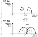
- a distribution width may increase or the distribution may move, so that the adjacent distributions may overlap with each other. This state is illustrated in FIGS. 9A and 9B .
- FIG. 9A and FIG. 9B are schematic views for describing a variation in threshold voltage distribution of one or more embodiments of the semiconductor memory device according to the first aspect.
- the threshold voltage distributions of “A” level and “B” level are as illustrated in FIG. 9A immediately after writing.
- the threshold voltage distributions spread out as illustrated in FIG. 9B due to factors including disturbance and the like.
- the read data of the memory cell transistor MT corresponding to an area of a hatched part becomes an error.
- the number of error bits exceeds the number of error correctable bits of the ECC circuit 13 , the data may not be sufficiently corrected.
- a voltage at which overlapping of the threshold voltage distributions of two levels becomes small is set as a new read voltage so that the number of error bits is reduced.
- shift reading can be performed in which a voltage (for example, a voltage BRopt in FIG. 9 ) at the valley position where the overlapping of the threshold voltage distributions of two levels is minimized (e.g. is at, or is in the vicinity of, a local minima) is set as the read voltage.
- the Vth tracking is an operation for detecting such a valley position.
- FIG. 10A through FIG. 10C are schematic views for describing an outline of one or more embodiments of a Vth tracking operation of the semiconductor memory device according to the first aspect.
- FIG. 10A is a graph illustrating threshold voltage distributions of “A” level and “B” level as one example of the threshold voltage distribution of the memory cell transistor MT group.
- FIG. 10B is a graph illustrating a transition of the number (the number of on-cells) of memory cells to be turned on for a predetermined read voltage.
- FIG. 10C is a histogram illustrating a variation in the number of on-cells in a read voltage range.
- FIGS. 10B and 10C are obtained by plotting values to correspond to the memory cell transistor MT group having the threshold voltage distributions of FIG. 10A .
- the number of on-cells abruptly increases at a voltage slightly lower than a voltage VA which is a median value of the “A” level, and as a result, dM/dV becomes a maximum (e.g. is at a local maxima).
- the median value is a voltage with the highest distribution probability of the threshold voltage in FIG. 10A , in which M represents the number of on-cells and V represents the read voltage to be applied to a selection word line WL.
- an increase rate of the number of on-cells decreases and becomes a minimum value (e.g. is at a local minima) at a certain value.
- the increase rate at the read voltage is about zero when the threshold voltage distribution of the “A” level and the threshold voltage distribution of the “B” level do not overlap with each other. Meanwhile, when both distributions overlap with each other, the corresponding increase rate becomes a predetermined non-zero minimum value (a value greater than 0). In addition, when the read voltage further increases, the increase rate of the number of on-cells increases again, and as a result, dM/dV becomes a maximum again (e.g. a local maxima) at a voltage slightly lower than the voltage VB which is a median value of the “B” level.
- the reading operation is performed using a read voltage V 1 .
- the number of on-cells in this case is set to M 1 .
- the reading operation is performed by using a voltage V 2 which is higher than the voltage V 1 by ⁇ V.
- the number of on-cells in this case is set to M 2 .
- the number of memory cell transistors MT newly turned on when the read voltage applied to the selection word line WL rises from V 1 to V 2 is (M 2 ⁇ M 1 ).
- the reading operation is performed by using a voltage V 3 which is higher than the voltage V 2 by ⁇ V.
- the number of on-cells in this case is set to M 3 .
- the number of memory cell transistors MT newly turned on when the read voltage applied to the selection word line WL rises from V 2 to V 3 is (M 3 ⁇ M 2 ).
- (M 2 ⁇ M 1 )>(M 3 ⁇ M 2 ) it is considered that the voltage at which dM/dV becomes the minimum is at least higher than the voltage V 2 .
- the reading operation is performed by using a voltage V 4 which is higher than the voltage V 3 by ⁇ V.
- V 4 which is higher than the voltage V 3 by ⁇ V.
- the histogram illustrated in FIG. 10C may be obtained.
- the variation of the number of on-cells is extracted, for example, by tracking a state in which the number of bits (bit count) in the read data per page varies by changing the read voltage. These operations are collectively referred to as the Vth tracking operation.
- FIG. 11 is a flowchart for describing the Vth tracking operation in the memory system according to the first aspect. Operations ST 21 to ST 30 illustrated in FIG. 11 can correspond to operation ST 4 in FIG. 8 .
- the controller 10 issues a lock command “XXh”.
- the semiconductor memory device 20 determines the temperature compensation value dV 2 based on the latest temperature information and fixes the temperature compensation value applied in the subsequent operation to the temperature compensation value dV 2 .
- Vlv is the standard value of the read voltage applied in a single-level reading.
- the controller 10 issues, to the semiconductor memory device 20 , a single-level reading command to designate the voltage Vlv as the standard value of the read voltage.
- the semiconductor memory device 20 executes the single-level reading in which the temperature compensation value dV 2 is applied to the standard value of the voltage Vlv.
- the semiconductor memory device 20 transmits the read data of the single-level reading to the controller 10 .
- the controller 10 calculates the bit count based on the read data of the single-level reading.
- operation ST 27 the controller 10 determines whether the loop processing is to be continued. Specifically, when the voltage Vlv is not higher than a voltage Vlv_max (or is lower than a voltage Vlv_max) (operation ST 27 ; No), the process proceeds to operation ST 28 to increment a voltage ⁇ lv to the voltage Vlv and thereafter, returns to operation ST 24 . Further, when the voltage Vlv is higher than the voltage Vlv_max (operation ST 27 ; Yes), the process proceeds to operation ST 29 .
- the controller 10 detects the valley position (operation ST 5 illustrated in FIG. 8 ) after completion of the calculation of the bit count in all single-level readings. As a result, the controller 10 may determine the read voltage of the read data at which a subsequent hard bit process (operation ST 8 illustrated in FIG. 8 ) is executed.
- FIG. 12 is a command sequence for describing one or more embodiments of a single-level reading operation of the semiconductor memory device according to the first aspect.
- the command sequence illustrated in FIG. 12 corresponds to operation ST 25 in FIG. 11 .
- the controller 10 issues a command “AAh”.
- the command “AAh” is a command for setting the single-level reading to be executed with respect to the semiconductor memory device 20 .
- the controller 10 issues an address over, for example, one cycle.
- the controller 10 issues the data DAT over, for example, one cycle.
- the data DAT includes, for example, information corresponding to a standard value (Vlv+ ⁇ lv) of the read voltage in the single-level reading.
- the controller 10 issues a prefix command “BBh”.
- the command “BBh” is a command for declaring that the controller 10 performs the single-level reading with respect to the semiconductor memory device 20 .
- the controller 10 issues a first read command “ooh” and subsequently issues addresses (including a column address, a block address, and a page address) over, for example, 5 cycles.
- the controller 10 issues a second read command “30h”.
- the sequencer 25 controls the voltage generation circuit 26 , the row decoder 27 , and/or the sense amplifier module 28 , to start the reading operation. Further, the logic control circuit 23 sets the signal /RB at the “L” level so as to notify the controller 10 that the semiconductor memory device 20 is in a busy state. During the reading operation, data for one page is read from an area corresponding to the address transmitted from the controller 10 . The logic control circuit 23 sets the signal /RB at the “H” level so as to notify the controller 10 that the semiconductor memory device 20 is in a ready state.
- the controller 10 When the semiconductor memory device 20 is in the ready state, the controller 10 repeatedly asserts the signal /RE. Whenever the signal /RE is toggled, the data read from the memory cell array 21 is transmitted to the controller 10 .
- the controller 10 when inputting the command to the semiconductor memory device 20 , the controller 10 asserts the signal CLE, when inputting the address, the controller 10 asserts the signal ALE, and when inputting the data, the controller 10 negates the signals CLE and ALE when the data is input. In addition, when a predetermined signal is input to the semiconductor memory device 20 , the controller 10 toggles the signal /WE.
- FIG. 13 is a schematic view for describing an outline of a soft bit reading operation of the semiconductor memory device according to the first aspect.
- FIG. 13 is a graph illustrating threshold voltage distributions of “A” level and “B” level as an example of threshold voltage distributions of the memory cell transistor MT group.
- the soft bit reading operation includes normal reading and plural shift readings shifted from the normal reading.
- the normal reading corresponds to the read voltage BR as the standard value.
- each of the plural shift readings corresponds to a read voltage (BR ⁇ 3 ⁇ , BR ⁇ 2 ⁇ , and BR ⁇ ) shifted by ⁇ 3 ⁇ , ⁇ 2 ⁇ , and ⁇ , for example, with respect to the read voltage BR of the normal reading as the standard value. That is, by the soft bit reading operation, the reading operation is executed by seven different read voltages (BR ⁇ 3 ⁇ , BR ⁇ 2 ⁇ , BR ⁇ , BR, BR+ ⁇ , BR+2 ⁇ , and BR+3 ⁇ ), for example, to read seven read data. In the soft bit reading operation, the plural reading operations are consecutively executed.
- the ECC circuit 13 estimates the threshold voltage distributions of the group of memory cell transistors MT by using the plural pieces of read data consecutively read by the soft bit reading operation. As a result, the ECC circuit 13 may perform error correction with higher accuracy than error correction based on only one read data.
- FIG. 14 is a flowchart for describing one or more embodiments of the soft bit reading operation of the memory system according to the first aspect. Operations ST 31 to ST 39 illustrated in FIG. 14 correspond to operation ST 9 in FIG. 8 .
- the controller 10 issues the lock command “XXh”.
- the semiconductor memory device 20 determines the temperature compensation value dV 2 based on the latest temperature information and fixes the temperature compensation value applied to the subsequent operation to the temperature compensation value dV 2 .
- the controller 10 issues, to the semiconductor memory device 20 , a shift reading command to designate a shift amount previously corresponding to a loop number n.
- the semiconductor memory device executes the shift reading to apply the temperature compensation value dV 2 to a read voltage shifted from the standard value of the normal reading by the shift amount corresponding to the loop number n.
- the semiconductor memory device 20 transmits the read data of the shift reading to the controller 10 .
- the controller 10 holds the read data of the shift reading in all loop numbers n.
- operation ST 36 the controller 10 determines whether the loop processing is to be continued. Specifically, when the loop number n is determined to be less than a value N (operation ST 36 ; no), the process proceeds to operation ST 36 to increment the loop number n and thereafter, returns to operation ST 34 . Further, when the loop number n is equal to or larger than the value N (operation ST 36 ; Yes), the process proceeds to operation ST 38 .
- FIG. 15 is a table for describing the soft bit reading operation of the semiconductor memory device according to the first aspect.
- FIG. 15 illustrates, for example, a relationship between the loop number n and the shift amount applied to the shift reading executed at the loop number n.
- the value N is 6
- the shift amount is set to “0”, and the same read voltage as that of the normal reading is applied as the standard value.
- the shift amount is set to “ ⁇ ”, and a value smaller by ⁇ than the read voltage of the normal reading is applied as the read voltage.
- the shift amount is set to “ ⁇ 2 ⁇ ”, and a value smaller by 2 ⁇ than the read voltage of the normal reading is applied as the read voltage.
- the shift amount is set to “ ⁇ 3 ⁇ ”, and a value smaller by 3 ⁇ than the read voltage of the normal reading is applied as the read voltage.
- the shift amount is set to “ ⁇ ”, and a value larger by ⁇ than the read voltage of the normal reading is applied as the read voltage.
- the shift amount is set to “2 ⁇ ”, and a value larger by 2 ⁇ than the read voltage of the normal reading is applied as the read voltage.
- the shift amount is set to “3 ⁇ ”, and a value larger by 3 ⁇ than the read voltage of the normal reading is applied as the read voltage.
- FIG. 16 is a command sequence for describing one or more embodiments of a shift reading operation of the semiconductor memory device according to the first aspect.
- the command sequence illustrated in FIG. 16 corresponds to operation ST 35 in FIG. 14 .
- the controller 10 first issues a prefix command “CCh”.
- the command “CCh” is a command for declaring that the controller 10 performs the shift reading with respect to the semiconductor memory device 20 .
- the controller 10 issues the address, for example, over one cycle.
- the controller 10 issues a DAC (D/A converter) value which is a value corresponding to the shift amount to the read voltage of the normal reading over, for example, four cycles.
- the DAC value is, for example, an indication value when the controller 10 designates the shift amount of the read voltage in the semiconductor memory device 20 .
- the controller 10 issues a command “DDh” and a first read command “00h” and transmits the issued command “DDh” and first read command “00h” to the semiconductor memory device 20 , as in the normal reading.
- the command “DDh” indicates which page the subsequent address corresponds to. For example, upon receiving consecutive commands “01h” and “00h”, the semiconductor memory device 20 recognizes that it is a lower page read, and upon receiving the commands “02h” and “00h”, the semiconductor memory device 20 recognizes that it is a middle page read, and upon receiving commands “03h” and “00h”, the semiconductor memory device 20 recognizes that it is an upper page read.
- the controller 10 subsequently issues the addresses (including the column address, the block address, and the page address) over, for example, 5 cycles. Thereafter, the controller 10 issues a second read command “30h”.
- the sequencer 25 controls the voltage generation circuit 26 , the row decoder 27 , and/or the sense amplifier module 28 , to start the reading operation.
- the logic control circuit 23 sets the signal /RB at the “L” level so as to notify the controller 10 that the semiconductor memory device 20 is in the busy state.
- data for one page is read from an area corresponding to the address transmitted from the controller 10 .
- the logic control circuit 23 sets the signal /RB at the “H” level so as to notify the controller 10 that the semiconductor memory device 20 is in a ready state.
- the characteristics of a memory cell transistor vary depending on a temperature environment during an operation. Therefore, when performing the writing operation and the reading operation, the parameters such as the voltage applied to the memory cell transistor according to the temperature are corrected by a temperature compensation value. As a result, the variation of the characteristics of the memory cell transistor according to the temperature change may be accounted for. Furthermore, it is possible to avoid a situation where reliability is greatly influenced by an operating environment.
- the read data may include a bit error exceeding a correction capability of the ECC circuit.
- techniques such as Vth tracking and soft bit reading are used as techniques for improving the reliability of the read data and reducing the bit errors to the extent that the bit errors are capable of being corrected by the second error correction. Both the Vth tracking and the soft bit reading continuously perform the plural reading operations in order to obtain optimum read data.
- FIG. 17 is a schematic view for describing an outline of an operation of the semiconductor memory device according to a comparative example.
- the shift amount of the read voltage during consecutive plural reading operations is not constant. Specifically, the shift amount between the read voltage BR and the read voltage BR+ ⁇ is different from the shift amount between the other read voltages.
- the soft bit decoding processing by the ECC circuit 13 is executed assuming that the same temperature compensation value dV is applied to all read voltages. That is, for example, the ECC circuit 13 executes the soft bit decoding processing on the premise that the shift amount between all read voltages is constant. For this reason, when the state as illustrated in the example of FIG. 17 occurs, the reliability of the soft bit decoding processing by the ECC circuit 13 decreases, and as a result, there is a possibility that optimum error correction will not be performed.
- the sequencer 25 upon receiving the lock command “XXh”, determines the temperature compensation value dV 2 according to the temperature based on the temperature information of the temperature after receiving the lock command “XXh”. Then, the sequencer 25 locks the updating of the temperature compensation value dV to a value different from the temperature compensation value dV 2 .
- the lock command “XXh” is consecutively received before the plural data reading operations such as the Vth tracking and the soft bit read, the temperature compensation value dV 2 is prevented from being updated in the course of plural times of data reading. Therefore, it is possible to suppress the lowering of the reliability precision of the subsequent ECC and further to suppress the deterioration of the reading accuracy of the data.
- the sequencer 25 Upon receiving the unlock command “YYh”, the sequencer 25 resumes the updating of the temperature compensation value dV. As a result, the temperature compensation value dV 2 locked once may be updated again. Therefore, the compensation value dV based on the latest temperature information may be applied in the operation after the Vth tracking or the soft bit reading is terminated.
- the controller 10 issues the lock command “XXh” when the error correction by the ECC circuit 13 is unsuccessful.
- the Vth tracking or the soft bit reading operation fixed to the temperature compensation value dV 2 may be promptly executed with respect to the read data for which error correction is unsuccessful.
- the controller 10 After issuing the unlock command “YYh”, the controller 10 executes the error correction by the ECC circuit 13 . As a result, the reading operation using the optimum read voltage obtained by the Vth tracking may be executed using the latest temperature compensation value.
- the controller 10 executes the error correction by the ECC circuit 13 after the soft bit reading operation is terminated. As a result, it is possible to perform the error correction based on plural pieces of read data obtained by the soft bit reading operation.
- the present disclosure is not limited to the embodiments according to the first aspect described herein, and various modifications to the first aspect may be made. According to the first aspect, descriptions have been made of a case where 3 bits are capable of being held per memory cell transistor MT (TLC: Triple Level Cell), but the first aspect is not limited thereto.
- the memory cell transistor MT may hold 2 bits (MLC: Multi Level Cell), or may hold 4 bits or more.
- the voltage applied to a word line selected for the A level reading operation is, for example, between 0 V and about 0.55 V.
- the corresponding voltage is not limited thereto, and may be in any range selected from about 0.1 V to about 0.24 V, about 0.21 V to about 0.31 V, about 0.31 V to about 0.4 V, about 0.4 V to about 0.5 V, and about 0.5 V to about 0.55 V.
- the voltage applied to a word line selected for the B level reading operation is, for example, between about 1.5 V and about 2.3 V.
- the corresponding voltage is not limited thereto and may be in any range selected from about 1.75 V to about 1.8 V, about 1.8 V to about 1.95 V, about 1.95 V to about 2.1 V, and about 2.1 V to about 2.3 V.
- the voltage applied to a word line selected for the C level reading operation is, for example, between about 3.0 V and about 4.0 V.
- the corresponding voltage is not limited thereto and may be in any range selected from about 3.0 V to about 3.2 V, about 3.2 V to about 3.4 V, about 3.4 V to about 3.5 V, about 3.5 V to about 3.7 V, and about 3.7 V to about 4.0 V.
- a reading operation time (tR) may be in any range selected from, for example, about 25 microseconds ( ⁇ s) to about 38 ⁇ s, about 38 ⁇ s to about 70 ⁇ s, and about 70 ⁇ s to about 80 ⁇ s.
- the writing operation includes a program operation and a verifying operation.
- the voltage initially applied to a word line selected during the program operation is, for example, between about 13.7 V and about 14.3 V.
- the corresponding voltage is not limited thereto, and may be in any range selected from, for example, about 13.7 V to about 14.0 V and about 14.0 V to about 14.7 V.
- the voltage initially applied to a selected word line when writing an odd-numbered word line and the voltage initially applied to a selected word line when writing an even-numbered word line may be changed.
- a step-up voltage may be set to, for example, about 0.5 V.
- the voltage applied to a non-selected word line may be, for example, between about 7.0 V and about 7.3 V.
- the corresponding voltage is not limited thereto, and may be, for example, between about 7.3 V and about 8.4 V or about 7.0 V or less.
- a pass voltage applied may be changed depending on whether the non-selected word line is an odd-numbered word line or an even-numbered word line.
- a writing operation time (tProg) may be in any range selected from, for example, about 1700 ⁇ s to about 1800 ⁇ s, about 1800 ⁇ s to about 1900 ⁇ s, and about 1900 ⁇ s to about 2000 ⁇ s.
- a voltage initially applied to a well which is formed on a semiconductor substrate and above which a memory cell is arranged, is, for example, between about 12 V and about 13.7 V.
- the voltage is not limited thereto, and may be in any range selected from, for example, about 13.7 V to about 14.8 V, about 14.8 V to about 19.0 V, about 19.0 to about 19.8 V, and about 19.8 V to about 21 V.
- An erasing operation time may be in any range selected from, for example, about 3000 ⁇ s to about 4000 ⁇ s, about 4000 ⁇ s to about 5000 ⁇ s, and about 4000 ⁇ s to about 9000 ⁇ s.
- the memory cell has a charge storage layer disposed on the semiconductor substrate (silicon substrate) through a tunnel insulating film having a film thickness of about 4 nanometers (nm) to about 10 nm.
- the charge storage layer may have a stacking structure of an insulating film of silicon nitride (SiN) or silicon oxynitride (SiON) having a film thickness of about 2 nm to about 3 nm and polysilicon having a film thickness of about 3 nm to about 8 nm. Further, a metal such as Ru may be added to the polysilicon.
- the insulating film is formed on the charge storage layer.
- the insulating film has a silicon oxide film having a film thickness of about 4 nm to about 10 nm and sandwiched between, for example, a lower high-k film having a film thickness of about 3 nm to about 10 nm and an upper high-k film having a film thickness of about 3 nm to about 10 nm.
- a lower high-k film having a film thickness of about 3 nm to about 10 nm
- an upper high-k film having a film thickness of about 3 nm to about 10 nm.
- the high-k film hafnium oxide (HfO) or the like may be exemplified.
- the film thickness of the silicon oxide film may be thicker than the film thickness of the high-k film.
- a control electrode having a film thickness of about 30 nm to about 70 nm is formed through a work function adjusting material having a film thickness of about 3 nm to about 10 nm.
- the work function adjusting material is a metal oxide film such as tantalum oxide (TaO), or a metal nitride film such as tantalum nitride (TaN).
- tungsten (W) or the like may be used.
- An air gap may be formed between memory cells.
- the term “about” is used to describe and account for small variations.
- the term “about” can refer to instances in which the event or circumstance occurs precisely as well as instances in which the event or circumstance occurs to a close approximation.
- the term “about” can refer to a range of variation less than or equal to ⁇ 10% of that numerical value, such as less than or equal to ⁇ 5%, less than or equal to ⁇ 4%, less than or equal to ⁇ 3%, less than or equal to ⁇ 2%, less than or equal to ⁇ 1%, less than or equal to ⁇ 0.5%, less than or equal to ⁇ 0.1%, or less than or equal to ⁇ 0.05%.
- a component provided “on,” “above,” or “over” another component can encompass cases where the former component is directly on (e.g., in physical contact with) the latter component, as well as cases where one or more intervening components are located between the former component and the latter component.
Landscapes
- Engineering & Computer Science (AREA)
- Microelectronics & Electronic Packaging (AREA)
- Computer Hardware Design (AREA)
- Read Only Memory (AREA)
Abstract
Description
Claims (10)
Applications Claiming Priority (2)
| Application Number | Priority Date | Filing Date | Title |
|---|---|---|---|
| JP2017-049975 | 2017-03-15 | ||
| JP2017049975A JP2018156696A (en) | 2017-03-15 | 2017-03-15 | Semiconductor memory device and memory system |
Publications (2)
| Publication Number | Publication Date |
|---|---|
| US20180268891A1 US20180268891A1 (en) | 2018-09-20 |
| US10692563B2 true US10692563B2 (en) | 2020-06-23 |
Family
ID=63520256
Family Applications (1)
| Application Number | Title | Priority Date | Filing Date |
|---|---|---|---|
| US15/695,866 Active 2037-10-23 US10692563B2 (en) | 2017-03-15 | 2017-09-05 | Semiconductor memory device and memory system |
Country Status (2)
| Country | Link |
|---|---|
| US (1) | US10692563B2 (en) |
| JP (1) | JP2018156696A (en) |
Cited By (1)
| Publication number | Priority date | Publication date | Assignee | Title |
|---|---|---|---|---|
| US20220301632A1 (en) * | 2021-03-19 | 2022-09-22 | Kioxia Corporation | Semiconductor storage device |
Families Citing this family (9)
| Publication number | Priority date | Publication date | Assignee | Title |
|---|---|---|---|---|
| US10496450B2 (en) * | 2017-05-22 | 2019-12-03 | Sandisk Technologies Llc | Selective temperature compensation |
| US10922017B2 (en) * | 2018-08-07 | 2021-02-16 | Micron Technology, Inc. | Memories for reading data corresponding to multiple addresses associated with a read command |
| KR102696810B1 (en) * | 2019-04-03 | 2024-08-21 | 에스케이하이닉스 주식회사 | Storage device and operating method thereof |
| JP2021044043A (en) | 2019-09-13 | 2021-03-18 | キオクシア株式会社 | Memory system |
| JP2021111427A (en) | 2020-01-15 | 2021-08-02 | キオクシア株式会社 | Storage device and control method thereof |
| JP2022050898A (en) | 2020-09-18 | 2022-03-31 | キオクシア株式会社 | Memory system and control method of memory system |
| CN113380309B (en) * | 2021-07-08 | 2025-11-11 | 英韧科技股份有限公司 | Method for searching optimal reading voltage and flash memory system |
| KR20240084838A (en) * | 2022-12-07 | 2024-06-14 | 삼성전자주식회사 | Non-volatile memory device, storage device having the same, and operating method thereof |
| US12430206B2 (en) * | 2023-05-19 | 2025-09-30 | Micron Technology, Inc. | Temperature sensor management during error handling operations in a memory sub-system |
Citations (7)
| Publication number | Priority date | Publication date | Assignee | Title |
|---|---|---|---|---|
| US20090310408A1 (en) * | 2008-06-13 | 2009-12-17 | Samsung Electronics Co., Ltd. | Memory system and method of accessing a semiconductor memory device |
| US20140071761A1 (en) | 2012-09-10 | 2014-03-13 | Sandisk Technologies Inc. | Non-volatile storage with joint hard bit and soft bit reading |
| US20150042488A1 (en) * | 2013-08-09 | 2015-02-12 | Utilidata, Inc. | Systems and methods for estimating conservation allocation with partial ami |
| US20160103625A1 (en) | 2013-06-20 | 2016-04-14 | Kabushiki Kaisha Toshiba | Device, host apparatus, host system, and memory system |
| US20160239235A1 (en) * | 2015-02-17 | 2016-08-18 | Woonjae Chung | Storage devices, memory systems and operating methods thereof |
| US20160266972A1 (en) | 2015-03-10 | 2016-09-15 | Kabushiki Kaisha Toshiba | Memory controller, storage device and decoding method |
| US20180061504A1 (en) * | 2016-08-26 | 2018-03-01 | Samsung Electronics Co., Ltd. | Non-Volatile Memory Devices Having Temperature and Location Dependent Word Line Operating Voltages |
-
2017
- 2017-03-15 JP JP2017049975A patent/JP2018156696A/en active Pending
- 2017-09-05 US US15/695,866 patent/US10692563B2/en active Active
Patent Citations (7)
| Publication number | Priority date | Publication date | Assignee | Title |
|---|---|---|---|---|
| US20090310408A1 (en) * | 2008-06-13 | 2009-12-17 | Samsung Electronics Co., Ltd. | Memory system and method of accessing a semiconductor memory device |
| US20140071761A1 (en) | 2012-09-10 | 2014-03-13 | Sandisk Technologies Inc. | Non-volatile storage with joint hard bit and soft bit reading |
| US20160103625A1 (en) | 2013-06-20 | 2016-04-14 | Kabushiki Kaisha Toshiba | Device, host apparatus, host system, and memory system |
| US20150042488A1 (en) * | 2013-08-09 | 2015-02-12 | Utilidata, Inc. | Systems and methods for estimating conservation allocation with partial ami |
| US20160239235A1 (en) * | 2015-02-17 | 2016-08-18 | Woonjae Chung | Storage devices, memory systems and operating methods thereof |
| US20160266972A1 (en) | 2015-03-10 | 2016-09-15 | Kabushiki Kaisha Toshiba | Memory controller, storage device and decoding method |
| US20180061504A1 (en) * | 2016-08-26 | 2018-03-01 | Samsung Electronics Co., Ltd. | Non-Volatile Memory Devices Having Temperature and Location Dependent Word Line Operating Voltages |
Cited By (1)
| Publication number | Priority date | Publication date | Assignee | Title |
|---|---|---|---|---|
| US20220301632A1 (en) * | 2021-03-19 | 2022-09-22 | Kioxia Corporation | Semiconductor storage device |
Also Published As
| Publication number | Publication date |
|---|---|
| US20180268891A1 (en) | 2018-09-20 |
| JP2018156696A (en) | 2018-10-04 |
Similar Documents
| Publication | Publication Date | Title |
|---|---|---|
| US11790986B2 (en) | Semiconductor storage device and memory system including semiconductor storage device and controller | |
| US10692563B2 (en) | Semiconductor memory device and memory system | |
| US11763893B2 (en) | Memory system | |
| US11367489B2 (en) | Multi-bit memory system with adaptive read voltage controller | |
| US11170857B2 (en) | Semiconductor memory device that performs successive tracking reads during an operation to read one page | |
| US10026492B2 (en) | Multi-die programming with die-jumping induced periodic delays | |
| US10643715B2 (en) | Semiconductor memory device and memory system configured to perform tracking read on first memory cells followed by shift read on second memory cells using read voltage correction value determined during the tracking read | |
| US10860251B2 (en) | Semiconductor memory device | |
| US8737128B2 (en) | Semiconductor memory device and method of operating the same | |
| JP2019053806A (en) | Memory system and memory system control method | |
| US10714171B2 (en) | NAND flash memory system storing multi-bit data and read/write control method thereof | |
| CN117746947A (en) | Memory system |
Legal Events
| Date | Code | Title | Description |
|---|---|---|---|
| FEPP | Fee payment procedure |
Free format text: ENTITY STATUS SET TO UNDISCOUNTED (ORIGINAL EVENT CODE: BIG.); ENTITY STATUS OF PATENT OWNER: LARGE ENTITY |
|
| AS | Assignment |
Owner name: TOSHIBA MEMORY CORPORATION, JAPAN Free format text: ASSIGNMENT OF ASSIGNORS INTEREST;ASSIGNORS:LI, SHAN;HARA, KEIGO;REEL/FRAME:043761/0943 Effective date: 20170913 |
|
| STPP | Information on status: patent application and granting procedure in general |
Free format text: NON FINAL ACTION MAILED |
|
| STPP | Information on status: patent application and granting procedure in general |
Free format text: RESPONSE TO NON-FINAL OFFICE ACTION ENTERED AND FORWARDED TO EXAMINER |
|
| STPP | Information on status: patent application and granting procedure in general |
Free format text: NOTICE OF ALLOWANCE MAILED -- APPLICATION RECEIVED IN OFFICE OF PUBLICATIONS |
|
| STPP | Information on status: patent application and granting procedure in general |
Free format text: PUBLICATIONS -- ISSUE FEE PAYMENT VERIFIED |
|
| STCF | Information on status: patent grant |
Free format text: PATENTED CASE |
|
| AS | Assignment |
Owner name: K.K. PANGEA, JAPAN Free format text: MERGER;ASSIGNOR:TOSHIBA MEMORY CORPORATION;REEL/FRAME:055659/0471 Effective date: 20180801 Owner name: KIOXIA CORPORATION, JAPAN Free format text: CHANGE OF NAME AND ADDRESS;ASSIGNOR:TOSHIBA MEMORY CORPORATION;REEL/FRAME:055669/0001 Effective date: 20191001 Owner name: TOSHIBA MEMORY CORPORATION, JAPAN Free format text: CHANGE OF NAME AND ADDRESS;ASSIGNOR:K.K. PANGEA;REEL/FRAME:055669/0401 Effective date: 20180801 |
|
| MAFP | Maintenance fee payment |
Free format text: PAYMENT OF MAINTENANCE FEE, 4TH YEAR, LARGE ENTITY (ORIGINAL EVENT CODE: M1551); ENTITY STATUS OF PATENT OWNER: LARGE ENTITY Year of fee payment: 4 |