US10690972B2 - Liquid crystal display device - Google Patents
Liquid crystal display device Download PDFInfo
- Publication number
- US10690972B2 US10690972B2 US15/928,665 US201815928665A US10690972B2 US 10690972 B2 US10690972 B2 US 10690972B2 US 201815928665 A US201815928665 A US 201815928665A US 10690972 B2 US10690972 B2 US 10690972B2
- Authority
- US
- United States
- Prior art keywords
- electrode
- slit
- pixel
- contact hole
- liquid crystal
- Prior art date
- Legal status (The legal status is an assumption and is not a legal conclusion. Google has not performed a legal analysis and makes no representation as to the accuracy of the status listed.)
- Active, expires
Links
Images


Classifications
-
- G—PHYSICS
- G02—OPTICS
- G02F—OPTICAL DEVICES OR ARRANGEMENTS FOR THE CONTROL OF LIGHT BY MODIFICATION OF THE OPTICAL PROPERTIES OF THE MEDIA OF THE ELEMENTS INVOLVED THEREIN; NON-LINEAR OPTICS; FREQUENCY-CHANGING OF LIGHT; OPTICAL LOGIC ELEMENTS; OPTICAL ANALOGUE/DIGITAL CONVERTERS
- G02F1/00—Devices or arrangements for the control of the intensity, colour, phase, polarisation or direction of light arriving from an independent light source, e.g. switching, gating or modulating; Non-linear optics
- G02F1/01—Devices or arrangements for the control of the intensity, colour, phase, polarisation or direction of light arriving from an independent light source, e.g. switching, gating or modulating; Non-linear optics for the control of the intensity, phase, polarisation or colour
- G02F1/13—Devices or arrangements for the control of the intensity, colour, phase, polarisation or direction of light arriving from an independent light source, e.g. switching, gating or modulating; Non-linear optics for the control of the intensity, phase, polarisation or colour based on liquid crystals, e.g. single liquid crystal display cells
- G02F1/133—Constructional arrangements; Operation of liquid crystal cells; Circuit arrangements
- G02F1/1333—Constructional arrangements; Manufacturing methods
- G02F1/1343—Electrodes
- G02F1/134309—Electrodes characterised by their geometrical arrangement
- G02F1/134363—Electrodes characterised by their geometrical arrangement for applying an electric field parallel to the substrate, i.e. in-plane switching [IPS]
-
- G—PHYSICS
- G02—OPTICS
- G02F—OPTICAL DEVICES OR ARRANGEMENTS FOR THE CONTROL OF LIGHT BY MODIFICATION OF THE OPTICAL PROPERTIES OF THE MEDIA OF THE ELEMENTS INVOLVED THEREIN; NON-LINEAR OPTICS; FREQUENCY-CHANGING OF LIGHT; OPTICAL LOGIC ELEMENTS; OPTICAL ANALOGUE/DIGITAL CONVERTERS
- G02F1/00—Devices or arrangements for the control of the intensity, colour, phase, polarisation or direction of light arriving from an independent light source, e.g. switching, gating or modulating; Non-linear optics
- G02F1/01—Devices or arrangements for the control of the intensity, colour, phase, polarisation or direction of light arriving from an independent light source, e.g. switching, gating or modulating; Non-linear optics for the control of the intensity, phase, polarisation or colour
- G02F1/13—Devices or arrangements for the control of the intensity, colour, phase, polarisation or direction of light arriving from an independent light source, e.g. switching, gating or modulating; Non-linear optics for the control of the intensity, phase, polarisation or colour based on liquid crystals, e.g. single liquid crystal display cells
- G02F1/133—Constructional arrangements; Operation of liquid crystal cells; Circuit arrangements
- G02F1/1333—Constructional arrangements; Manufacturing methods
- G02F1/1337—Surface-induced orientation of the liquid crystal molecules, e.g. by alignment layers
- G02F1/133711—Surface-induced orientation of the liquid crystal molecules, e.g. by alignment layers by organic films, e.g. polymeric films
- G02F1/133723—Polyimide, polyamide-imide
-
- G—PHYSICS
- G02—OPTICS
- G02F—OPTICAL DEVICES OR ARRANGEMENTS FOR THE CONTROL OF LIGHT BY MODIFICATION OF THE OPTICAL PROPERTIES OF THE MEDIA OF THE ELEMENTS INVOLVED THEREIN; NON-LINEAR OPTICS; FREQUENCY-CHANGING OF LIGHT; OPTICAL LOGIC ELEMENTS; OPTICAL ANALOGUE/DIGITAL CONVERTERS
- G02F1/00—Devices or arrangements for the control of the intensity, colour, phase, polarisation or direction of light arriving from an independent light source, e.g. switching, gating or modulating; Non-linear optics
- G02F1/01—Devices or arrangements for the control of the intensity, colour, phase, polarisation or direction of light arriving from an independent light source, e.g. switching, gating or modulating; Non-linear optics for the control of the intensity, phase, polarisation or colour
- G02F1/13—Devices or arrangements for the control of the intensity, colour, phase, polarisation or direction of light arriving from an independent light source, e.g. switching, gating or modulating; Non-linear optics for the control of the intensity, phase, polarisation or colour based on liquid crystals, e.g. single liquid crystal display cells
- G02F1/133—Constructional arrangements; Operation of liquid crystal cells; Circuit arrangements
- G02F1/1333—Constructional arrangements; Manufacturing methods
- G02F1/1343—Electrodes
- G02F1/13439—Electrodes characterised by their electrical, optical, physical properties; materials therefor; method of making
-
- G—PHYSICS
- G02—OPTICS
- G02F—OPTICAL DEVICES OR ARRANGEMENTS FOR THE CONTROL OF LIGHT BY MODIFICATION OF THE OPTICAL PROPERTIES OF THE MEDIA OF THE ELEMENTS INVOLVED THEREIN; NON-LINEAR OPTICS; FREQUENCY-CHANGING OF LIGHT; OPTICAL LOGIC ELEMENTS; OPTICAL ANALOGUE/DIGITAL CONVERTERS
- G02F1/00—Devices or arrangements for the control of the intensity, colour, phase, polarisation or direction of light arriving from an independent light source, e.g. switching, gating or modulating; Non-linear optics
- G02F1/01—Devices or arrangements for the control of the intensity, colour, phase, polarisation or direction of light arriving from an independent light source, e.g. switching, gating or modulating; Non-linear optics for the control of the intensity, phase, polarisation or colour
- G02F1/13—Devices or arrangements for the control of the intensity, colour, phase, polarisation or direction of light arriving from an independent light source, e.g. switching, gating or modulating; Non-linear optics for the control of the intensity, phase, polarisation or colour based on liquid crystals, e.g. single liquid crystal display cells
- G02F1/133—Constructional arrangements; Operation of liquid crystal cells; Circuit arrangements
- G02F1/136—Liquid crystal cells structurally associated with a semi-conducting layer or substrate, e.g. cells forming part of an integrated circuit
- G02F1/1362—Active matrix addressed cells
- G02F1/136213—Storage capacitors associated with the pixel electrode
-
- G—PHYSICS
- G02—OPTICS
- G02F—OPTICAL DEVICES OR ARRANGEMENTS FOR THE CONTROL OF LIGHT BY MODIFICATION OF THE OPTICAL PROPERTIES OF THE MEDIA OF THE ELEMENTS INVOLVED THEREIN; NON-LINEAR OPTICS; FREQUENCY-CHANGING OF LIGHT; OPTICAL LOGIC ELEMENTS; OPTICAL ANALOGUE/DIGITAL CONVERTERS
- G02F1/00—Devices or arrangements for the control of the intensity, colour, phase, polarisation or direction of light arriving from an independent light source, e.g. switching, gating or modulating; Non-linear optics
- G02F1/01—Devices or arrangements for the control of the intensity, colour, phase, polarisation or direction of light arriving from an independent light source, e.g. switching, gating or modulating; Non-linear optics for the control of the intensity, phase, polarisation or colour
- G02F1/13—Devices or arrangements for the control of the intensity, colour, phase, polarisation or direction of light arriving from an independent light source, e.g. switching, gating or modulating; Non-linear optics for the control of the intensity, phase, polarisation or colour based on liquid crystals, e.g. single liquid crystal display cells
- G02F1/133—Constructional arrangements; Operation of liquid crystal cells; Circuit arrangements
- G02F1/136—Liquid crystal cells structurally associated with a semi-conducting layer or substrate, e.g. cells forming part of an integrated circuit
- G02F1/1362—Active matrix addressed cells
- G02F1/136227—Through-hole connection of the pixel electrode to the active element through an insulation layer
-
- G—PHYSICS
- G02—OPTICS
- G02F—OPTICAL DEVICES OR ARRANGEMENTS FOR THE CONTROL OF LIGHT BY MODIFICATION OF THE OPTICAL PROPERTIES OF THE MEDIA OF THE ELEMENTS INVOLVED THEREIN; NON-LINEAR OPTICS; FREQUENCY-CHANGING OF LIGHT; OPTICAL LOGIC ELEMENTS; OPTICAL ANALOGUE/DIGITAL CONVERTERS
- G02F1/00—Devices or arrangements for the control of the intensity, colour, phase, polarisation or direction of light arriving from an independent light source, e.g. switching, gating or modulating; Non-linear optics
- G02F1/01—Devices or arrangements for the control of the intensity, colour, phase, polarisation or direction of light arriving from an independent light source, e.g. switching, gating or modulating; Non-linear optics for the control of the intensity, phase, polarisation or colour
- G02F1/13—Devices or arrangements for the control of the intensity, colour, phase, polarisation or direction of light arriving from an independent light source, e.g. switching, gating or modulating; Non-linear optics for the control of the intensity, phase, polarisation or colour based on liquid crystals, e.g. single liquid crystal display cells
- G02F1/133—Constructional arrangements; Operation of liquid crystal cells; Circuit arrangements
- G02F1/136—Liquid crystal cells structurally associated with a semi-conducting layer or substrate, e.g. cells forming part of an integrated circuit
- G02F1/1362—Active matrix addressed cells
- G02F1/136286—Wiring, e.g. gate line, drain line
-
- G—PHYSICS
- G02—OPTICS
- G02F—OPTICAL DEVICES OR ARRANGEMENTS FOR THE CONTROL OF LIGHT BY MODIFICATION OF THE OPTICAL PROPERTIES OF THE MEDIA OF THE ELEMENTS INVOLVED THEREIN; NON-LINEAR OPTICS; FREQUENCY-CHANGING OF LIGHT; OPTICAL LOGIC ELEMENTS; OPTICAL ANALOGUE/DIGITAL CONVERTERS
- G02F1/00—Devices or arrangements for the control of the intensity, colour, phase, polarisation or direction of light arriving from an independent light source, e.g. switching, gating or modulating; Non-linear optics
- G02F1/01—Devices or arrangements for the control of the intensity, colour, phase, polarisation or direction of light arriving from an independent light source, e.g. switching, gating or modulating; Non-linear optics for the control of the intensity, phase, polarisation or colour
- G02F1/13—Devices or arrangements for the control of the intensity, colour, phase, polarisation or direction of light arriving from an independent light source, e.g. switching, gating or modulating; Non-linear optics for the control of the intensity, phase, polarisation or colour based on liquid crystals, e.g. single liquid crystal display cells
- G02F1/133—Constructional arrangements; Operation of liquid crystal cells; Circuit arrangements
- G02F1/136—Liquid crystal cells structurally associated with a semi-conducting layer or substrate, e.g. cells forming part of an integrated circuit
- G02F1/1362—Active matrix addressed cells
- G02F1/1368—Active matrix addressed cells in which the switching element is a three-electrode device
-
- G—PHYSICS
- G02—OPTICS
- G02F—OPTICAL DEVICES OR ARRANGEMENTS FOR THE CONTROL OF LIGHT BY MODIFICATION OF THE OPTICAL PROPERTIES OF THE MEDIA OF THE ELEMENTS INVOLVED THEREIN; NON-LINEAR OPTICS; FREQUENCY-CHANGING OF LIGHT; OPTICAL LOGIC ELEMENTS; OPTICAL ANALOGUE/DIGITAL CONVERTERS
- G02F1/00—Devices or arrangements for the control of the intensity, colour, phase, polarisation or direction of light arriving from an independent light source, e.g. switching, gating or modulating; Non-linear optics
- G02F1/01—Devices or arrangements for the control of the intensity, colour, phase, polarisation or direction of light arriving from an independent light source, e.g. switching, gating or modulating; Non-linear optics for the control of the intensity, phase, polarisation or colour
- G02F1/13—Devices or arrangements for the control of the intensity, colour, phase, polarisation or direction of light arriving from an independent light source, e.g. switching, gating or modulating; Non-linear optics for the control of the intensity, phase, polarisation or colour based on liquid crystals, e.g. single liquid crystal display cells
- G02F1/137—Devices or arrangements for the control of the intensity, colour, phase, polarisation or direction of light arriving from an independent light source, e.g. switching, gating or modulating; Non-linear optics for the control of the intensity, phase, polarisation or colour based on liquid crystals, e.g. single liquid crystal display cells characterised by the electro-optical or magneto-optical effect, e.g. field-induced phase transition, orientation effect, guest-host interaction or dynamic scattering
-
- G—PHYSICS
- G02—OPTICS
- G02F—OPTICAL DEVICES OR ARRANGEMENTS FOR THE CONTROL OF LIGHT BY MODIFICATION OF THE OPTICAL PROPERTIES OF THE MEDIA OF THE ELEMENTS INVOLVED THEREIN; NON-LINEAR OPTICS; FREQUENCY-CHANGING OF LIGHT; OPTICAL LOGIC ELEMENTS; OPTICAL ANALOGUE/DIGITAL CONVERTERS
- G02F1/00—Devices or arrangements for the control of the intensity, colour, phase, polarisation or direction of light arriving from an independent light source, e.g. switching, gating or modulating; Non-linear optics
- G02F1/01—Devices or arrangements for the control of the intensity, colour, phase, polarisation or direction of light arriving from an independent light source, e.g. switching, gating or modulating; Non-linear optics for the control of the intensity, phase, polarisation or colour
- G02F1/13—Devices or arrangements for the control of the intensity, colour, phase, polarisation or direction of light arriving from an independent light source, e.g. switching, gating or modulating; Non-linear optics for the control of the intensity, phase, polarisation or colour based on liquid crystals, e.g. single liquid crystal display cells
- G02F1/133—Constructional arrangements; Operation of liquid crystal cells; Circuit arrangements
- G02F1/1333—Constructional arrangements; Manufacturing methods
- G02F1/1337—Surface-induced orientation of the liquid crystal molecules, e.g. by alignment layers
- G02F1/133707—Structures for producing distorted electric fields, e.g. bumps, protrusions, recesses, slits in pixel electrodes
-
- G—PHYSICS
- G02—OPTICS
- G02F—OPTICAL DEVICES OR ARRANGEMENTS FOR THE CONTROL OF LIGHT BY MODIFICATION OF THE OPTICAL PROPERTIES OF THE MEDIA OF THE ELEMENTS INVOLVED THEREIN; NON-LINEAR OPTICS; FREQUENCY-CHANGING OF LIGHT; OPTICAL LOGIC ELEMENTS; OPTICAL ANALOGUE/DIGITAL CONVERTERS
- G02F1/00—Devices or arrangements for the control of the intensity, colour, phase, polarisation or direction of light arriving from an independent light source, e.g. switching, gating or modulating; Non-linear optics
- G02F1/01—Devices or arrangements for the control of the intensity, colour, phase, polarisation or direction of light arriving from an independent light source, e.g. switching, gating or modulating; Non-linear optics for the control of the intensity, phase, polarisation or colour
- G02F1/13—Devices or arrangements for the control of the intensity, colour, phase, polarisation or direction of light arriving from an independent light source, e.g. switching, gating or modulating; Non-linear optics for the control of the intensity, phase, polarisation or colour based on liquid crystals, e.g. single liquid crystal display cells
- G02F1/133—Constructional arrangements; Operation of liquid crystal cells; Circuit arrangements
- G02F1/1333—Constructional arrangements; Manufacturing methods
- G02F1/1343—Electrodes
- G02F1/134309—Electrodes characterised by their geometrical arrangement
- G02F1/134318—Electrodes characterised by their geometrical arrangement having a patterned common electrode
-
- G—PHYSICS
- G02—OPTICS
- G02F—OPTICAL DEVICES OR ARRANGEMENTS FOR THE CONTROL OF LIGHT BY MODIFICATION OF THE OPTICAL PROPERTIES OF THE MEDIA OF THE ELEMENTS INVOLVED THEREIN; NON-LINEAR OPTICS; FREQUENCY-CHANGING OF LIGHT; OPTICAL LOGIC ELEMENTS; OPTICAL ANALOGUE/DIGITAL CONVERTERS
- G02F1/00—Devices or arrangements for the control of the intensity, colour, phase, polarisation or direction of light arriving from an independent light source, e.g. switching, gating or modulating; Non-linear optics
- G02F1/01—Devices or arrangements for the control of the intensity, colour, phase, polarisation or direction of light arriving from an independent light source, e.g. switching, gating or modulating; Non-linear optics for the control of the intensity, phase, polarisation or colour
- G02F1/13—Devices or arrangements for the control of the intensity, colour, phase, polarisation or direction of light arriving from an independent light source, e.g. switching, gating or modulating; Non-linear optics for the control of the intensity, phase, polarisation or colour based on liquid crystals, e.g. single liquid crystal display cells
- G02F1/133—Constructional arrangements; Operation of liquid crystal cells; Circuit arrangements
- G02F1/1333—Constructional arrangements; Manufacturing methods
- G02F1/1343—Electrodes
- G02F1/134309—Electrodes characterised by their geometrical arrangement
- G02F1/134372—Electrodes characterised by their geometrical arrangement for fringe field switching [FFS] where the common electrode is not patterned
-
- G—PHYSICS
- G02—OPTICS
- G02F—OPTICAL DEVICES OR ARRANGEMENTS FOR THE CONTROL OF LIGHT BY MODIFICATION OF THE OPTICAL PROPERTIES OF THE MEDIA OF THE ELEMENTS INVOLVED THEREIN; NON-LINEAR OPTICS; FREQUENCY-CHANGING OF LIGHT; OPTICAL LOGIC ELEMENTS; OPTICAL ANALOGUE/DIGITAL CONVERTERS
- G02F1/00—Devices or arrangements for the control of the intensity, colour, phase, polarisation or direction of light arriving from an independent light source, e.g. switching, gating or modulating; Non-linear optics
- G02F1/01—Devices or arrangements for the control of the intensity, colour, phase, polarisation or direction of light arriving from an independent light source, e.g. switching, gating or modulating; Non-linear optics for the control of the intensity, phase, polarisation or colour
- G02F1/13—Devices or arrangements for the control of the intensity, colour, phase, polarisation or direction of light arriving from an independent light source, e.g. switching, gating or modulating; Non-linear optics for the control of the intensity, phase, polarisation or colour based on liquid crystals, e.g. single liquid crystal display cells
- G02F1/133—Constructional arrangements; Operation of liquid crystal cells; Circuit arrangements
- G02F1/136—Liquid crystal cells structurally associated with a semi-conducting layer or substrate, e.g. cells forming part of an integrated circuit
- G02F1/1362—Active matrix addressed cells
- G02F1/136222—Colour filters incorporated in the active matrix substrate
-
- G—PHYSICS
- G02—OPTICS
- G02F—OPTICAL DEVICES OR ARRANGEMENTS FOR THE CONTROL OF LIGHT BY MODIFICATION OF THE OPTICAL PROPERTIES OF THE MEDIA OF THE ELEMENTS INVOLVED THEREIN; NON-LINEAR OPTICS; FREQUENCY-CHANGING OF LIGHT; OPTICAL LOGIC ELEMENTS; OPTICAL ANALOGUE/DIGITAL CONVERTERS
- G02F1/00—Devices or arrangements for the control of the intensity, colour, phase, polarisation or direction of light arriving from an independent light source, e.g. switching, gating or modulating; Non-linear optics
- G02F1/01—Devices or arrangements for the control of the intensity, colour, phase, polarisation or direction of light arriving from an independent light source, e.g. switching, gating or modulating; Non-linear optics for the control of the intensity, phase, polarisation or colour
- G02F1/13—Devices or arrangements for the control of the intensity, colour, phase, polarisation or direction of light arriving from an independent light source, e.g. switching, gating or modulating; Non-linear optics for the control of the intensity, phase, polarisation or colour based on liquid crystals, e.g. single liquid crystal display cells
- G02F1/133—Constructional arrangements; Operation of liquid crystal cells; Circuit arrangements
- G02F1/136—Liquid crystal cells structurally associated with a semi-conducting layer or substrate, e.g. cells forming part of an integrated circuit
- G02F1/1362—Active matrix addressed cells
- G02F1/1368—Active matrix addressed cells in which the switching element is a three-electrode device
- G02F1/13685—Top gates
-
- G—PHYSICS
- G02—OPTICS
- G02F—OPTICAL DEVICES OR ARRANGEMENTS FOR THE CONTROL OF LIGHT BY MODIFICATION OF THE OPTICAL PROPERTIES OF THE MEDIA OF THE ELEMENTS INVOLVED THEREIN; NON-LINEAR OPTICS; FREQUENCY-CHANGING OF LIGHT; OPTICAL LOGIC ELEMENTS; OPTICAL ANALOGUE/DIGITAL CONVERTERS
- G02F1/00—Devices or arrangements for the control of the intensity, colour, phase, polarisation or direction of light arriving from an independent light source, e.g. switching, gating or modulating; Non-linear optics
- G02F1/01—Devices or arrangements for the control of the intensity, colour, phase, polarisation or direction of light arriving from an independent light source, e.g. switching, gating or modulating; Non-linear optics for the control of the intensity, phase, polarisation or colour
- G02F1/13—Devices or arrangements for the control of the intensity, colour, phase, polarisation or direction of light arriving from an independent light source, e.g. switching, gating or modulating; Non-linear optics for the control of the intensity, phase, polarisation or colour based on liquid crystals, e.g. single liquid crystal display cells
- G02F1/137—Devices or arrangements for the control of the intensity, colour, phase, polarisation or direction of light arriving from an independent light source, e.g. switching, gating or modulating; Non-linear optics for the control of the intensity, phase, polarisation or colour based on liquid crystals, e.g. single liquid crystal display cells characterised by the electro-optical or magneto-optical effect, e.g. field-induced phase transition, orientation effect, guest-host interaction or dynamic scattering
- G02F1/13706—Devices or arrangements for the control of the intensity, colour, phase, polarisation or direction of light arriving from an independent light source, e.g. switching, gating or modulating; Non-linear optics for the control of the intensity, phase, polarisation or colour based on liquid crystals, e.g. single liquid crystal display cells characterised by the electro-optical or magneto-optical effect, e.g. field-induced phase transition, orientation effect, guest-host interaction or dynamic scattering the liquid crystal having positive dielectric anisotropy
-
- G02F2001/134318—
-
- G02F2001/134372—
-
- G02F2001/136222—
-
- G02F2001/13685—
-
- G02F2001/13706—
-
- G—PHYSICS
- G02—OPTICS
- G02F—OPTICAL DEVICES OR ARRANGEMENTS FOR THE CONTROL OF LIGHT BY MODIFICATION OF THE OPTICAL PROPERTIES OF THE MEDIA OF THE ELEMENTS INVOLVED THEREIN; NON-LINEAR OPTICS; FREQUENCY-CHANGING OF LIGHT; OPTICAL LOGIC ELEMENTS; OPTICAL ANALOGUE/DIGITAL CONVERTERS
- G02F2201/00—Constructional arrangements not provided for in groups G02F1/00 - G02F7/00
- G02F2201/12—Constructional arrangements not provided for in groups G02F1/00 - G02F7/00 electrode
- G02F2201/121—Constructional arrangements not provided for in groups G02F1/00 - G02F7/00 electrode common or background
-
- G—PHYSICS
- G02—OPTICS
- G02F—OPTICAL DEVICES OR ARRANGEMENTS FOR THE CONTROL OF LIGHT BY MODIFICATION OF THE OPTICAL PROPERTIES OF THE MEDIA OF THE ELEMENTS INVOLVED THEREIN; NON-LINEAR OPTICS; FREQUENCY-CHANGING OF LIGHT; OPTICAL LOGIC ELEMENTS; OPTICAL ANALOGUE/DIGITAL CONVERTERS
- G02F2201/00—Constructional arrangements not provided for in groups G02F1/00 - G02F7/00
- G02F2201/12—Constructional arrangements not provided for in groups G02F1/00 - G02F7/00 electrode
- G02F2201/122—Constructional arrangements not provided for in groups G02F1/00 - G02F7/00 electrode having a particular pattern
-
- G—PHYSICS
- G02—OPTICS
- G02F—OPTICAL DEVICES OR ARRANGEMENTS FOR THE CONTROL OF LIGHT BY MODIFICATION OF THE OPTICAL PROPERTIES OF THE MEDIA OF THE ELEMENTS INVOLVED THEREIN; NON-LINEAR OPTICS; FREQUENCY-CHANGING OF LIGHT; OPTICAL LOGIC ELEMENTS; OPTICAL ANALOGUE/DIGITAL CONVERTERS
- G02F2201/00—Constructional arrangements not provided for in groups G02F1/00 - G02F7/00
- G02F2201/12—Constructional arrangements not provided for in groups G02F1/00 - G02F7/00 electrode
- G02F2201/123—Constructional arrangements not provided for in groups G02F1/00 - G02F7/00 electrode pixel
-
- G—PHYSICS
- G02—OPTICS
- G02F—OPTICAL DEVICES OR ARRANGEMENTS FOR THE CONTROL OF LIGHT BY MODIFICATION OF THE OPTICAL PROPERTIES OF THE MEDIA OF THE ELEMENTS INVOLVED THEREIN; NON-LINEAR OPTICS; FREQUENCY-CHANGING OF LIGHT; OPTICAL LOGIC ELEMENTS; OPTICAL ANALOGUE/DIGITAL CONVERTERS
- G02F2202/00—Materials and properties
- G02F2202/10—Materials and properties semiconductor
- G02F2202/104—Materials and properties semiconductor poly-Si
Definitions
- the present invention relates to a display device, specifically a high definition liquid crystal display device, which is used for VR (virtual Reality) etc.
- a liquid crystal display device has a TFT substrate, a counter substrate opposing to the TFT substrate, and a liquid crystal layer sandwiched between the TFT substrate and the counter substrate.
- the TFT substrate has plural pixels arranged in matrix form; each of the pixels has a pixel electrode and a thin film transistor (TFT).
- TFT thin film transistor
- the liquid crystal display device has a problem in viewing angle characteristics.
- IPS In Plane Switching
- a transmittance of light in the pixel becomes a problem. Namely, the ratio of the area of the contact hole or video signal lines, etc. that doesn't contribute to formation of displays becomes relatively bigger in the pixel.
- the domain is generated due to a reverse rotation of the liquid crystal molecules in certain places; the light doesn't transmit the boundary between the domain and the normal region, thus, the a generation of the domain further decreases the transmittance of the pixel.
- the patent document 1 Japanese patent laid open 2011-186010 discloses the IPS type liquid crystal display device wherein the common electrode has a plurality of slits that extend in a horizontal direction; the slits are formed in common in horizontally and adjacently arranged pixels to avoid decreasing of transmittance of light in the pixel.
- the patent document 2 discloses the IPS type liquid crystal display device wherein two areas, where rotating directions of liquid crystal are different to each other, are formed in a pixel; in each of the areas, the common electrode has a plurality of slits that extend in a direction slightly tilted from the horizontal direction, the slits are formed in common in horizontally and adjacently arranged pixels to avoid decreasing of transmittance of light in the pixel; the tilting directions of the slits in each of the areas are symmetry to each other with respect to the horizontal direction.
- a market of the VR (virtual Reality) is expected to expand.
- a liquid crystal display device that is used in VR (virtual Reality) has to satisfy both characteristics of high definition, which is 1000 ppi (pixels per inch), and high response speed. There are some problems to overcome to realize such a liquid crystal display device.
- One problem is a decrease in transmittance due to downsizing of the pixels. In addition to that, a domain, which is generated in the transmitting area in the pixel, decreases a transmittance of the pixel.
- Another problem is a decrease in holding capacitance.
- the holding capacitance is formed between the pixel electrode and the common electrode; when the pixel becomes smaller, the pixel electrode becomes smaller; as a result, the holding capacitance decreases. If the holding capacitance becomes smaller, the flickers in the display occur.
- Moving pictures are often viewed in VR (virtual Reality), and etc., consequently, a speed of response of the liquid crystal molecules must be increased, thus, kinds of materials of the liquid crystal are limited.
- the purpose of the present invention is to solve those problems, thus, to realize a super high definition liquid crystal display device that can display natural images.
- the present invention overcomes the above explained problem; the concrete measures are as follows.
- a liquid crystal display device comprising: a scan line extends in a first direction, a video signal line extends in a direction of tilting angle of ⁇ 1 with respect to a second direction that is perpendicular to the first direction, and after crossing the scan line, the video signal line extends in a direction of tilting angle of ⁇ 1 with respect to the second direction, a pixel is formed in an area surrounded by scan line and the video signal line;
- the pixel includes: a thin film transistor, a flattening film that covers the thin film transistor, a first electrode formed on the flattening film, a second electrode formed over the first electrode via a first insulating film, a third electrode formed over the second electrode via a second insulating film, and a contact hole that is formed in the flattening film to connect the second electrode and the thin film transistor,
- the first electrode is formed in common in plural pixels
- the third electrode is formed in common in plural pixels
- the third electrode has a slit in parallel to the video signal line; the slit is formed continuously in a plural pixels aligned in the second direction.
- FIG. 1A is a perspective view according to the present invention.
- FIG. 1B is a plan view that shows the structure of the second substrate
- FIG. 2A is a plan view of the pixel according to first embodiment
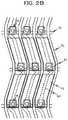
- FIG. 2B is a plan view of the pixel according to first embodiment
- FIG. 3A is a cross sectional view along A-A′ line in FIG. 2A ;
- FIG. 3B is a cross sectional view along B-B′ line in FIG. 2A ;
- FIG. 4A is a model that shows behavior of the liquid crystal molecules
- FIG. 4B is a model that shows behavior of the liquid crystal molecules
- FIG. 5 is a model of domain
- FIG. 6A is a plan view of the pixel according to second embodiment
- FIG. 6B is a plan view of the pixel according to second embodiment
- FIG. 7 is a plan view of the pixel according to third embodiment.
- FIG. 8A is a cross sectional view along A-A′ line in FIG. 7 ;
- FIG. 8B is a cross sectional view along B-B′ line in FIG. 7 ;
- FIG. 9A is a plan view of the pixel according to fourth embodiment.
- FIG. 9B is a plan view of the pixel according to fourth embodiment.
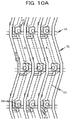
- FIG. 10A is a plan view of the pixel according to fifth embodiment.
- FIG. 10B is a plan view of the pixel according to fifth embodiment.
- FIG. 11A is a cross sectional view along A-A′ line in FIG. 12A ;
- FIG. 11B is a cross sectional view along B-B′ line in FIG. 12A ;
- FIG. 12A is a plan view of the pixel according to sixth embodiment.
- FIG. 12B is a plan view of the pixel according to sixth embodiment.
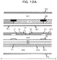
- FIG. 13A is a cross sectional view along A-A′ line in FIG. 2A according to seventh embodiment
- FIG. 13B is a cross sectional view along B-B′ line in FIG. 2A according to seventh embodiment
- FIG. 14A is a plan view of the pixel according to eighth embodiment.
- FIG. 14B is a cross sectional view along A-A′ line in FIG. 14A according to eighth embodiment
- FIG. 14C is a plan view of the pixel according to eighth embodiment.
- FIG. 15 is a plan view of first comparative example
- FIG. 16 is a plan view of second comparative example
- FIG. 17A is a plan view of an example according to the present invention.
- FIG. 17B is a plan view of third comparative example
- FIG. 18A is a plan view of fourth comparative example
- FIG. 18B is a plan view of another fourth comparative example.
- a necessary holding capacitance per one pixel is determined by a leak of the thin film transistor; therefore, the same capacitance as in a case of 500 ppi (pixels per inch) is necessary even in a case of 1000 ppi.
- One example of the present invention is to have the following structure in order to maintain a necessary holding capacitance; that is to make the electrode a three layer structure, which enables to use the thin film transistor that includes poly-silicon in a channel, which is the most popular thin film transistor.
- either one of the common electrode or the pixel electrode (herein after source electrode) that is nearer to the thin film transistor is made solid plane shaped, and another electrode is made the electrode of comb-like or the electrode having a slit.
- the present invention adds another solid plane shaped electrode between the solid plane electrode and the thin film transistor, thus makes three layer structures, wherein a capacitance between the solid plane electrode and another solid plane electrode is added as the holding capacitance.
- Positive type liquid crystal of low viscosity is appropriate to improve the response speed, however, the positive type liquid crystal molecules tend to generate domain at both edges of the pixel.
- the rotating direction of the liquid crystal molecules in the domain is reverse compared with the rotating direction of the liquid crystal molecules in the regular area.
- Each of the domains is separated by the regular region; however, a boundary between the regular region and the domain is very unstable. For example, if domains at edges of the pixel combine to each other, the boundary disappear; thus, the structure becomes stable; however, in a pixel of high definition display, a width of regular region is narrow; thus, some domains tend to combine to each other, on the contrary, some domains do not combine to each other, thus, structure becomes unstable.
- the bending portion of electrode is adopted for the pixel electrode to avoid domains at the end of the pixel, rotating angle of the liquid crystal molecules in response to electric field becomes smaller, thus, a transmittance of the pixel decreases. Further, if the bending portion of electrode is adopted in a high definition pixel, a relative ratio of the bending area becomes bigger in the pixel, thus, the transmittance is further decreased.
- the present invention has the structure that the domain is less likely to occur, thus the necessary transmittance can be maintained even in a super high definition display.
- the domain since the domain is less likely to occur, liberty in choosing the liquid crystal materials increases; consequently, the liquid crystal materials that enable high speed response can be adopted.
- FIG. 1A is a perspective view that shows the structure of the liquid crystal display device
- FIG. 1B is a plan view of the liquid crystal display device according to the present invention.
- the first substrate SU 1 and the second substrate SU 2 sandwich the liquid crystal layer LC (see FIG. 3 ); the backlight BL is disposed to on the back of the second substrate SU 2 .
- FIG. 1B is a plan view of the second substrate SU 2 viewed from the side of the liquid crystal layer LC.
- the peripheral circuit PC and the connection portion CN are formed at outer side of the display area DP, and the driving circuit is connected via the connection portion CN.
- the backlight BL comprises a light guide and a light source; the light source is a structure that the phosphor is laminated over the blue light emitting diode, consequently, the light source emits white light; the light source is disposed on a side surface of the light guide.
- FIGS. 2A and 2B are plan views of the pixel according to the present invention.
- FIG. 2A is a plan view that includes six pixels and their surroundings on the second substrate SU 2 , namely, the video signal line SL, the scan line GL, the second electrode E 2 (see FIG. 2B ), the polysilicon layer PS, the base electrode layer BS, the contact hole CH.
- the polysilicon layer PS which is formed at the cross area of the video signal line SL and the scan line GL, connects with the second electrode E 2 at the contact hole CH via the base electrode layer BS.
- the contact hole CH is made through the second flattening film OC 2 , the fourth insulating film IL 4 and the first electrode E 1 ;
- the contact hole CH in FIGS. 2A and 2B is represented by the hole formed in the second flattening film OC 2 .
- the first direction X and the second direction Y cross to each other, the scan line GL extends in the first direction X.
- the video signal line SL extends in the second direction Y, however tilting with a first angle of ⁇ in a first region and tilting with a second tilting angle of ⁇ in a second region with respect to the second direction Y.
- FIG. 2B is a plan view that includes, the video signal line SL, the scan line GL, the base electrode layer BS, the contact hole CH, the second electrode E 2 and the third electrode E 3 on the second substrate SU 2 .
- the first electrode E 1 is approximately a solid plane shape, but openings are formed with a certain spatial pitch in it; the opening includes the contact hole CH in it, thus, the first electrode E 1 does not exist in the contact hole CH.
- the second electrode E 2 exists in the area surrounded by the video signal line SL and the scan line GL; The second electrode E 2 may overlap with both of or either of the video signal line SL and the scan line GL in a plan view; the second electrode E 2 exists in the contact hole CH, too.
- the third electrode E 3 is also approximately a solid plane shape, but slits, which extend approximately parallel to the video signal line SL, are formed in the pixels as depicted by broken line in FIG. 2B : the slit contains the contact hole CH in it.
- the third electrode E 3 is separated by the slit in the first direction X, however, a wiring, which is not shown in the figures, connects the separated third electrodes E 3 to each other; thus, the third electrode E 3 can be supplied with a common voltage.
- FIG. 3A is a cross sectional view along the line A-A′ in FIG. 2A ;
- FIG. 3B a cross sectional view along the line B-B′ in FIG. 2A .
- FIG. 3A is a cross sectional view at the center of the pixel;
- FIG. 3B is a cross sectional view that includes the active element.
- the first substrate SU 1 is borosilicate glass of a thickness of 0.2 mm.
- the first alignment film AL 1 , the first flattening film OC 1 , the color filter CF, the black matrix BM are formed in this order from the liquid crystal layer LC side on the first substrate SU 1 .
- the second substrate SU 2 is borosilicate glass of a thickness of 0.2 mm like the first substrate.
- the following layers are formed in the order from the liquid crystal layer LC side; namely, the second alignment film AL 2 , the third electrode E 3 , the fifth insulating film IL 5 , the second electrode E 2 , the fourth insulating film IL 4 , the first electrode E 1 , the second flattening film OC 2 , the base electrode layer BS, the video signal line SL, the third insulating film IL 3 , the second insulating film IL 2 , the scan line GL, the first insulating film IL 1 , the polysilicon layer PS, the second under coat UC 2 , the first undercoat UC 1 and the light shield layer LS.
- the first alignment film AL 1 is a polyimide film that is processed by optical alignment method; the first flattening film OC 1 is a non-photosensitive transparent organic film; the black matrix BM is formed by negative type photoresist that includes black pigments.
- the color filter CF includes the red color filter RC, the green color filter GC and the blue color filter BC, which are repeated in certain spatial pitch.
- the red color filter RC, the green color filter GC and the blue color filter BC are all plane and stipe shaped and formed by negative type photoresist, wherein the red color filter RC contains red pigments, the green color filter contains green pigments and the blue color filter contains blue pigments.
- the laminating order of the color filter CF and the black matrix BM is not necessarily in this order. For example, if the black matrix BM is formed nearer to the liquid crystal layer LC, a color mixture due to the viewing angle can be decreased.
- the second alignment film AL 2 is a polyimide film that is processed by optical alignment method, as the same as the first alignment film AL 1 ; the first electrode E 1 , the second electrode E 2 and third electrode E 3 are all formed by transparent metal-oxide conductive film as e.g. ITO (Indium Tin Oxide).
- the second electrode E 2 is applied with a voltage of video signal; the first electrode E 1 and the third electrode E 3 are applied with the common voltage.
- the overlapping portion between the first electrode E 1 and the second electrode E 2 , and the overlapping portion between the second electrode E 2 and the third electrode E 3 form the holding capacitance.
- the fourth insulating film IL 4 and the fifth insulating film IL 5 are silicon nitride films, which are formed by low temperature process.
- the fifth insulating film IL 5 is sandwiched by the third electrode E 3 and the second electrode E 2 , which forms the holding capacitance;
- the fourth insulating film IL 4 is sandwiched by the second electrode E 2 and the first electrode E 1 , which also forms the holding capacitance.
- the second flattening film OC 2 is a positive organic photoresist;
- the base electrode layer BS and the video signal line SL, formed on the same layer, are made of e.g. a laminated film of three layers of Ti, Aluminum (or Aluminum alloy), and Ti.
- the third insulating film IL 3 is a silicon nitride film; the second insulating film IL 2 and the first insulating film IL 1 are silicon oxide films.
- the scan line GL and the light shield layer LS are made of e.g. molybdenum tungsten alloy film; the poly silicon layer PS is that amorphous silicon is transformed to poly silicon by laser annealing; the first under coat UC 1 is a silicon nitride film and the second under coast UC 2 is a silicon oxide film.
- Post spacers which are not shown in FIGS. 2A-3B , are set at cross areas of the video signal lines SL and the scan lines GL to hold the liquid crystal layer LC and to maintain the thickness of the liquid crystal layer uniform in the display area.
- the post spacers are columnar organic films that are formed on the first substrate SU 1 or on the second substrate SU 2 .
- the post spacers can be formed on both of the first substrate SU 1 and the second substrate SU 2 .
- the post spacers are made rod-like; the rod-like spacer of the first substrate SU 1 and the rod-like spacer of the second substrate SU 2 cross each other in a plan view, then the friction area is limited on the tops of the spacers when the pressing force is applied to the substrate SU 1 or SU 2 ; consequently, a degradation of contrast can be avoided.
- the liquid crystal layer LC is formed by the material of positive dielectric anisotropy, which dielectric constant of the liquid crystal molecules in the alignment direction is bigger than that in the direction perpendicular to the alignment direction; the liquid crystal layer formed by the material of positive dielectric anisotropy has high electrical resistance and reveals nematic phase in a wide temperature range.
- the alignment state of the liquid crystal layer LC is homogeneous when no voltage is applied;
- FIG. 2A shows a model of the alignment state of the liquid crystal molecules LCM 1 and LCM 2 , which are depicted by cylinders.
- the liquid crystal display device of the present embodiment is FFS (Fringe Field Switching) type, wherein the fringe field EF that is depicted by an arrow of dotted line in the liquid crystal layer LC in FIG. 3A . Accordingly, the liquid crystal molecules LCM 1 and LCM 2 in the liquid crystal layer LC rotate their alignment direction in a plane of the liquid crystal layer LC as depicted by arrows in FIG. 2A .
- the liquid crystal layer can be formed by the material of negative dielectric anisotropy, which dielectric constant of the liquid crystal molecules in the alignment direction is smaller than that in the direction perpendicular to the alignment direction; in that case, the alignment of the liquid crystal molecules LCM 1 and LCM 2 in the liquid crystal layer LC is rotated 90 degree with respect to the direction in FIG. 2A when no voltage is applied.
- the liquid crystal layer LC of a positive dielectric constant anisotropy has characteristics of a low viscosity and a superior response speed; the liquid crystal layer LC of a negative dielectric constant anisotropy has characteristics of more uniform alignment of the liquid crystal molecules when the voltage is applied, thus, gives a uniform and high transmittance.
- the first polarizing plate PL 1 is set on the upper side of the first substrate SU 1 and the second polarizing plate PL 2 is set on the lower side of the second substrate SU 2 .
- the absorbing axis of the first polarizing plate PL 1 and the absorbing axis of the second polarizing plate PL 2 are on a plane perpendicular to the normal axis of the liquid crystal panel; the absorbing axis of the second polarizing plate PL 2 is parallel to the initial alignment direction of the liquid crystal molecules.
- the voltage-brightness characteristics of the normally black type liquid crystal display device is established, which displays black when the voltage is not applied while the transmittance increases when the voltage is applied.
- the liquid crystal molecules change their alignment direction as rotating in the plane of the liquid crystal layer LC; under a certain viewing angle, yellowish display and bluish display appear alternatively in every 90 degree in azimuth direction.
- the pixel is made as parallelogram, the tilting angle of the parallelogram is made reverse between the adjacent pixels in the longitudinal direction.
- a pair of the pixels that the rotating angles of the liquid crystal molecules are in reverse direction to each other is adjacently repeated in the longitudinal direction, and further if the individual pixel is small enough, the coloring in the viewing angle is averaged. Therefore, the yellowish and the bluish are averaged and viewed as achromatic, consequently the problem of the coloring is eliminated.
- the electrode closest to the liquid crystal layer LC is comb like shape or plane shape having a slit.
- the third electrode E 3 corresponds to this electrode in this embodiment. Since the third electrode E 3 is applied with a common voltage it has a slit. When the liquid crystal display device becomes high definition display, only one slit can be formed in the pixel due to requirement of accuracy in manufacturing process.
- the base electrode layer BS is formed on the same layer as the video signal line SL is formed, manufacturing process can be simple; however, in a high definition display, the distances between the base electrode layer BS and each of the two video signal lines SL are made equal to avoid short. As a result, the base electrode layer BS is set at the center of the pixel in the lateral direction, consequently, the contact hole CH, which connects the base electrode layer BS and the second electrode E 2 cannot substantially deviate from the center of the pixel.
- the slit of the third electrode E 3 is formed after the contact hole CH is formed; concretely, the photoresist is coated on the ITO, which is formed on the fifth insulating film IL 5 .
- the diameter of the contact hole CH is limited so as to be less than a half of the width of the pixel.
- the thickness of the second flattening film must be thick enough to decrease parasitic capacitance between the video signal line SL and the first electrode E 1 .
- the photoresist flows into the contact hole CH, thus, the thickness of the photoresist becomes locally thick in the contact hole CH.
- the photoresist is patterned under a regular condition, in which the pattern is approximately the same as the pattern of the photo mask, the photoresist remains in the contact hole CH; on the contrary, when the photoresist is patterned under the condition that the photoresist in the contact hole CH is eliminated, the other portions where the photoresist is in regular thickness get significant over etching. Therefore, the boundary of the slit should not be formed in the contact hole CH; concretely, the contact hole CH is formed inside of the slit or the contact hole CH is formed outside of the slit. This embodiment is an example that the contact hole CH is formed inside of the slit.
- a metal line is formed to decrease the resistance of the common electrode; in this case the metal wring is formed superposing the video signal line SL in a plan view.
- the metal line can be formed to laminate on the third electrode E 3 .
- the rotating direction of the liquid crystal molecule is clock wise CW or anti-clock wise ACW is determined by the relation between the direction of the field EF and the initial alignment direction AD; the rotating direction is chosen so as that least rotating angle is necessary for the liquid crystal molecule to align with the field.
- the rotating angle is less in the anti-clock wise direction ACW, thus, the liquid crystal molecules in the liquid crystal layer LC rotate in the anti-clock wise direction.
- the notation E 3 in FIGS. 4A and 4B means the slit in the third electrode E 3 .
- the alignment angle is generally set approximately 10 degree to maintain the transmittance as big as possible as depicted in FIG. 4B .
- the difference in rotating angle between the clock wise CK direction and the anti-clock wise direction is small, thus, the domain, which is explained later, tends to appear.
- the directions of the field EF change 180 degree at the edge of the slit as depicted in FIG. 5 .
- point A and point E which is at an opposite side of the point A, are at the slit boundary; the direction of the field EF, along the boundary of the slit from point A to point B, rotates 180 degree. Therefore, the portion where a reverse direction is a smaller rotating direction for the liquid crystal molecule inevitably appears.
- FIG. 5 depicts examples of directions of the field at the edge of the slit, namely, at B point, C point and D point.
- the rotating angle in the anti-clock wise direction ACW is smaller at point A and point E of the edge of the slit, while the rotating angle in the clock wise direction CW is smaller at point B of the edge of the slit.
- the portion where the rotating direction is reverse is called the domain; the force to rotate in the clock wise direction CW and the force to rotate in the anti-clock wise direction ACW compete to each other at the boundary of the domain and the normal region; thus, the liquid crystal molecules in the liquid crystal layer LC cannot move.
- the characteristics of voltage—brightness characteristics is normally black, thus, the boundary becomes a black line.
- the domain boundary that is determined by the relation between the direction of the field EF and the initial alignment direction is depicted by thick line in FIG. 5 .
- the alignment of the liquid crystal molecule is nearly perpendicular to the direction of the field, the electrical energy is high; further the alignment energy is also high because the alignment directions of the liquid crystal molecule change drastically near the boundary. Therefore, the boundary between the domain and the normal region is very unstable, thus, the position of the boundary changes easily due to external stresses or thermal fluctuations; consequently, the area of the boundary may expand than the distribution of FIG. 5 , which is determined by the relation between the direction of the field EF and the initial alignment direction AD.
- the domain appears at both edges of the slit. For example, if two domains combine to each other, the boundary disappear, consequently, the liquid crystal layer LC becomes stable. Especially in high definition pixels, the pixel is small; therefore, the distance between the two domains at the edges of the slit is small, consequently, two domains ostensibly attract to each other, thus, the domains become more unstable. If the position of the domain is different in each of the pixels, the transmittance becomes different in each of the pixels, thus, unfavorable nonuniformity in brightness occurs. In addition, if the distribution of the domain changes in time, the nonuniformity looks like to be moving.
- the slit In order to fix the position of the domain at the edge of the slit, e.g. the slit can be bent at the edge of the slit to make rotating angle for the reverse rotation bigger.
- the rotating angle of the liquid crystal molecules LCM decreases in the normal direction when the field is applied in the liquid crystal layer LC as depicted in FIG. 4A ; thus, the transmittance at the bending portion of the slit decreases.
- the necessary size of the bending portion to stabilize the domain is constant regardless the size of the pixel, thus, high definition pixels get more influence of the decrease in transmittance.
- the shape of the bending portion is easily affected by that etching condition of the ITO is whether over etching or under etching.
- the bending portion does not have enough length; therefore, a surplus length of the bending portion must be taken as a tolerance, which results in further decrease in transmittance. Therefore, as depicted in FIG. 2B , if the slits are connected between the pixels, the bending portion of the slit can be further shifted to the edge of the pixel in the longitudinal direction.
- three electrodes of the first electrode E 1 , the second electrode E 2 and the third electrode E 3 are formed; the overlapping portion of the first electrode E 1 and the second electrode E 2 , and the overlapping portion of the second electrode E 2 and the third electrode E 3 form a holding capacitance; thus, enough holding capacitance can be formed even the area of the pixel is small; consequently displays without flicker can be realized.
- the third electrode E 3 is the common electrode; thus, a slit that is continuous in the pixels can be formed in the third electrode E 3 as depicted by the broken line in FIG. 2B .
- the slit which is shown by the broken line in FIG. 2B , contains the contact hole CH inside; the slit is located at the center of the pixel and is continuous in the pixels; the tilting angle of the contour of the slit is bigger at the boundary between the pixels in the longitudinal direction, thus, the above described problem in the high definition pixels can be solved.
- the slit can be formed stably without interfering with the contact hole CH; thus, the nonuniformity in brightness can be avoided since the domain is stabilized, and high transmittance in the pixel can be realized.
- FIGS. 6A and 6B are plan views of the pixel of the liquid crystal display device according to the present embodiment.
- FIG. 6A and FIG. 6B show the same structure;
- FIG. 6A shows the semiconductor layer PS while
- FIG. 6B shows the boundary (hole) of the first electrode E 1 , and the second electrode E 2 .
- the slit structure of the third electrode E 3 is changed to bypass the contact hole CH. Further, at the portion where the slit bypasses the contact hole CH, the tilting direction of the slit is made similar direction as the slit extends at the center of the pixel where the slit extends along the video signal line SL; thus, generation of the domain can be avoided at the bypass portion.
- the distribution of the height of the surface of the second flattening film OC 2 near the contact hole CH depends on the cross section of the color filter CF, if it is formed on the second substrate SU 2 , fluidity of the material for the second flattening film when it is coated, presence or absence of the middle bake in the baking process of the flattening film OC 2 . Therefore, there is a chance that the distribution of the height of the surface of the second flattening film OC 2 changes gradually from the center of the contact hole CH to outer region, and further the distributions can be different from pixel to pixel.
- the edge of the slit exists near the contact hole CH; consequently, the thickness of the photoresist for patterning the third electrode changes from pixel to pixel. As a result, there was a chance that the variation in dimension of the slit around the contact hole CH occurs.
- the color filter CF is set on the second substrate SU 2 , in contrast to the first embodiment, in which the color filter CF is formed on the first substrate SU 1 .
- FIG. 7 is a plan view of the second substrate SU 2 on which the video signal line SL, the scan line GL, the base electrode layer BS, the red color filter RC, the green color filter GC, the blue color filter BC, the contact hole CH and the third electrode E 3 are formed.
- FIG. 8A is a cross sectional view along A-A′ line of FIG. 7 ;
- FIG. 8B is a cross sectional view along B-B′ line of FIG. 7 .
- FIG. 8A is a cross sectional view at the center of the pixel while FIG. 8B is a cross sectional view including the active element.
- the first alignment film AL 1 , the first flattening film OC 1 and the black matrix BM are formed from the side of the liquid crystal layer LC on the first substrate SU 1 .
- the color filter CF is added between the second flattening film OC 2 and the third insulating film IL 3 on the second substrate SU 2 in the present embodiment.
- the plan view of the video signal line SL, the scan line GL, the second electrode E 2 , the polysilicon layer PS, the base electrode layer BS and the contact hole CH on the second substrate SU 2 in the liquid crystal display device according to the present embodiment is the same as FIG. 2A .
- the plan view of the video signal line SL, the scan line GL, the base electrode layer BS, the contact hole CH, the second electrode E 2 and the third electrode E 3 on the second substrate SU 2 in the liquid crystal display device according to the present embodiment is the same as FIG. 2B .
- the liquid crystal display device is the COA (Color Filter on Array) type, in which the color filter CF is formed on the same substrate as the active element is formed.
- the COA type has a merit to decrease the color mixture due to the viewing angle.
- the color mixture due to the viewing angle is a specific phenomenon when primary color is displayed in the FFS type liquid crystal display device; wherein the hue changes when viewing angle, in polar angle, is changed when viewed in the direction that the different color filters are arranged.
- the pixel and the color filter are set to correspond one to one. The color mixture due to the viewing angle occurs when the light passes the color filter that is not intended to pass.
- Forming the color filter CF on the array substrate can decrease a deviation between the color filter CF and the pixel, and further, can decrease the distance between the color filter CF and the pixel; therefore, the COA type has a merit in decreasing the color mixture due to the viewing angle.
- the COA type has a merit to overcome this problem. If color mixture due to the viewing angle doesn't occur, clear and pure color can be observed even viewed in an oblique direction to the screen.
- the contact hole CH is slightly deviated from the center between the two video signal lines SL compared with the structure of the first embodiment. Since, in a plan view, the contact hole CH is near the lower side of the pixel which is approximately parallelogram, in this embodiment, the contact hole CH is deviated to the direction reverse to the direction that the parallelogram tilts. In reverse to the above structure, if the contact hole CH is near the top of the pixel, the contact hole CH is deviated to the same direction as the direction that the parallelogram tilts; that is the case when FIG. 9A and FIG. 9B are seen from upside down direction.
- FIG. 9A and FIG. 9B are the plan views of the liquid crystal display device according to the present embodiment.
- FIG. 9A and FIG. 9B correspond to FIG. 2A and FIG. 2B of the first embodiment respectively.
- FIGS. 9A and 9B are plan views of the video signal line SL, the scan line GL, the base electrode layer BS, the contact hole CH, the second electrode E 2 and the third electrode E 3 on the second substrate SU 2 .
- a width of the slit of the third electrode E 3 is narrower at the center of the pixel, and is wider at area that includes the contact hole CH.
- the width of the slit at the area that includes the contact hole CH must be wide enough to include the contact hole CH inside.
- the slit in the center of the pixel and the slit in the region that includes contact hole CH are connected continuously, however in FIG. 2B , the tilt angle of one side edge of the slit changes so as to approach nearer to the vertical direction before the slit includes the contact hole CH, as a result the width of the slit increases at this region.
- the alignment of the liquid crystal molecules in the liquid crystal layer LC is changed; however, if the width of the slit is big, the edge of the slit becomes nearer to the boundary with the adjacent pixel; consequently, there is a chance that alignment of the liquid crystal molecules propagate to the adjacent pixel.
- the contact hole CH is covered and light shielded by the black matrix BM that is formed on the first substrate all, thus, color purity is not deteriorated even the width of the silt becomes bigger.
- the position of the contact hole CH is deviated from the center of the pixel in an amount of 1 micron. If the layout allows, the deviation can be more than 1 micron.
- the pixel is approximately parallelogram and the contact hole CH exists at the lower side of the pixel. The pixels in the upper row tilt in the right hand direction while the pixels in the lower row tilt in the left hand direction; the contact holes CH in the upper row are deviated 1 micron to the left and the contact holes CH in the lower row are deviated 1 micron to the right. Since the connection area between the base electrode layer BS and the contact hole CH is big enough, the connection between the base electrode layer BS and the second electrode E 2 can be maintained even in this case.
- FIGS. 9A and 9B are compared with FIGS. 2A and 2B , it is apparent that, in this embodiment, vertically extending length of the contour of the slit near the contact hole CH is shorter in FIGS. 9A and 9B ; thus, the area where the width of the slit is wider than the optimum value is decreased.
- range of choice of the liquid crystal material is enlarged with respect to the characteristics of birefringence; consequently, the liquid crystal material of low viscosity can be adopted, thus, response speed can be improved.
- the range of choice of the material is enlarged, as a result, the liquid crystal material of low viscosity can be adopted.
- the contact hole CH is slightly deviated from the center between the two video signal lines SL compared with the same structure of the second embodiment. Since the contact hole CH is near the bottom of the pixel, which is approximately parallelogram, in this embodiment, the contact hole CH is deviated in the direction reverse to the direction that the parallelogram tilts. In reverse to the above structure, if the contact hole CH is near the top of the pixel, the contact hole CH is deviated in the same direction as the direction that the parallelogram tilts; that is the case when FIG. 10A and FIG. 10B are seen from upside down direction.
- FIG. 10A and FIG. 10B correspond to FIG. 6A and FIG. 6B of the second embodiment respectively.
- FIGS. 10A and 10B are plan views of the video signal line SL, the scan line GL, the base electrode layer BS, the contact hole CH, the second electrode E 2 and the third electrode E 3 on the second substrate SU 2 .
- FIGS. 10A and 10B are compared with FIGS. 6A and 6B , it is apparent that the area of the slit of the third electrode E 3 to bypass the contact hole CH is decreased because the contact hole CH is deviated from the center of the base electrode layer BS.
- patterning of the slit of the third electrode E 3 can be more stable.
- the transmittance can be improved in this embodiment.
- the video signal line SL and the base electrode layer BS are formed on different layers compared with the structure of the first embodiment.
- the sixth insulating film IL 6 is formed between the video signal line SL and the base electrode layer BS; the contact hole for the connection between the poly-silicon layer PS and the base electrode layer BS is made through the sixth insulating film IL 6 .
- FIG. 11A is a cross sectional view at the center of the pixel while FIG. 11B is a cross sectional view at the area that includes the low temperature poly-silicon PS.
- FIG. 11A is a cross sectional view along the A-A′ line of FIG. 12A ;
- FIG. 11B is a cross sectional view along the B-B′ line of FIG. 12A .
- FIG. 12A corresponds to FIG. 2A while FIG. 12B corresponds to FIG. 2B . Comparing FIGS. 12A and 12B with FIGS. 2A and 2B , it is apparent that the distance between the video signal line SL and the base electrode layer BS is less in the present embodiment, namely, FIGS.
- the size of the pixel is diminished in this embodiment. Since the video signal line SL and the base electrode layer BS are formed on the different layers in this embodiment, a short between the video signal line SL and the base electrode layer BS does not occur; therefore, a high definition pixels that has narrower pixels than that of the first embodiment can be realized.
- parasitic capacitance between the video signal line SL and the base electrode layer BS should be decreased.
- the video signal line SL and the base electrode layer BS overlap in a plan view, the parasitic capacitance increases.
- the thickness of the sixth insulating film IL 6 is increased, the parasitic capacitance decreases; however, a contact becomes difficult between the base electrode layer BS and the poly-silicon layer PS. Therefore, the video signal line SL and the base electrode layer BS should be disposed so as not to overlap to each other in a plan view; further, it is best to set the base electrode layer BS at the center between the two video signal lines SL to decrease the parasitic capacitance as depicted in FIGS. 12A and 12B .
- the base electrode layer BS is at the center between the two video signal lines SL even when the video signal line SL and the base electrode layer BS are formed on the different layers.
- the contact hole CH is also at the center of the pixel; consequently, the portion of the slit that is not covered by the black matrix BM should be at the center of the pixel.
- the slit of the third electrode E 3 either includes the contact hole CH inside or bypasses the contact hole CH in a plan view; FIGS. 12 A and 12 B is are the former structure. In this case, too, the holding capacitance can be maintained, domain can be stably fixed, and further, high transmittance of the light can be attained.
- the seventh embodiment has a simpler layer structure as depicted in FIGS. 13A and 13B compared with the structure of the liquid crystal display device of the first embodiment.
- FIG. 13A is a cross sectional view at the center of the pixel while FIG. 13B is a cross sectional view at the area that includes the low temperature poly-silicon PS. Comparing FIGS. 13A and 13B with FIGS. 2A and 2B , it is apparent that the first electrode E 1 and the fourth insulating film IL 4 in FIGS. 2A and 2B are eliminated in FIGS. 13A and 13B .
- the holding capacitance is formed only by the overlapping portions between the first electrode E 1 and the second electrode E 2 ; however, in a high frequency display, the flicker will not occur since holding time is short.
- High-K film which has a high dielectric constant
- the material for the High-K film are aluminum oxide, Hafnium oxide, praseodymium oxide, etc.
- the first electrode E 1 is applied with the source voltage while the second electrode E 2 is applied with the common voltage; this structure is so called a common top structure.
- the contact hole CH exists at the center of the pixel, the portion, which is not covered by the black matrix BM, of the slit of the second electrode E 2 is located at the center of the pixel. Consequently, if the slit of the second electrode E 2 either includes a contact hole CH inside or bypasses the contact hole CH in a plan view, the domain can be stably fixed and high transmittance of light can be attained.
- the width of the slit is made as big as possible to include the second electrode E 2 inside of the slit in a plan view.
- the slit is wide enough to avoid overlapping of the second electrode E 2 and the third electrode E 3 , and further, to include the contact hole CH inside of the slit.
- the distance between the edge of the slit and the second electrode E 2 can be made bigger because the second electrode E 2 is formed inside of the slit.
- the holding capacitance becomes smaller; however, as depicted in FIG. 14B , a necessary amount of holding capacitance can be formed because the first electrode E 1 and the second electrode E 2 overlap.
- the contact hole CH is formed at the center between the two adjacent video signal lines SL.
- the video signal line SL meanders to left and right (in the first direction X), the contact holes CH also moves to left and right according to the meander of the video signal line SL; consequently, the contact hole CH that moves to the left and the contact hole CH that moves to the right with respect to the second direction Y are formed.
- left deviated contact hole CHL the contact hole CH moved to the right is called right deviated contact hole CHR.
- the left deviated contact hole CHL and the right deviated contact hole CHR are arranged alternatively in up and down direction, namely in the second direction Y, in FIG. 14A .
- the left deviated contact hole CHL and the right deviated contact hole CHR sandwich the scan line GL in the second direction, and are used to connect the second electrode E 2 in each of the pixels to the same video signal line SL.
- the slit has the right slit boundary E 3 R and the left slit boundary E 3 L.
- the right slit boundary E 3 R is formed in vicinity of the right hand edge of the left deviated contact hole CHL and the left slit boundary E 3 L is formed in vicinity of the left hand edge of the right deviated contact hole CHR to avoid overlapping of the contact hole CH and the slit boundaries E 3 R and E 3 L.
- FIG. 14C is the structure that countermeasures the above problem.
- the tilting angle of the slit boundary is changed from the tilting angle of the video signal line SL to make the width of the slit at the contact hole CH bigger, thus, to form enough space between the slit boundary and the pixel boundary in the main area including A-A′ line.
- the slit is formed between the adjacent two video signal lines SL; the second electrode E 2 is formed inside of the slit.
- the slit boundary is more apart from the adjacent pixel than that in FIG. 14A .
- the right slit boundary E 3 R which is near to the left deviated contact hole CHL, changes its direction from the second angle ⁇ to the second direction Y to avoid the right edge of the left deviated contact hole CHL.
- the right slit boundary E 3 R changes its direction, when it goes over the left deviated contact hole CHL, back to the second angle ⁇ ; the right slit boundary E 3 R changes its direction in an angle bigger than the first angle ⁇ near the scan line GL; the right slit boundary E 3 R changes its direction at the opening of the black matrix BM in the first angle ⁇ and extends along the second electrode E 2 until it goes over the right deviated contact hole CHR in the first angle ⁇ .
- the right slit boundary E 3 R changes its direction in an angle bigger than the second angle ⁇ with respect to the second direction Y, and it changes its direction near the opening of the black matrix BM in the second angle ⁇ .
- the second electrode E 2 also tilts at an angle bigger than the first angle ⁇ corresponding to the place where the right slit boundary E 3 R tilt with the first angle ⁇ .
- the left slit boundary E 3 L which is near to the left deviated contact hole CHL, extends with the second angle ⁇ until it goes over the left deviated contact hole CHL; it changes its direction in an angle bigger than the first angle ⁇ near the scan line GL.
- the left slit boundary E 3 L changes its direction at the opening of the black matrix BM in the first angle ⁇ and extends along the second electrode E 2 to the right deviated contact hole CHR; when the left slit boundary E 3 L approaches to the right deviated contact hole CHR, it changes its direction from the first angle ⁇ to the second direction Y to avoid the left edge of the right deviated contact hole CHR.
- the angle in absolute value of the right slit boundary with respect to the second direction Y decreases, thus, the width of the slit in the first direction X becomes bigger.
- the left slit boundary E 3 L changes its direction, when it goes over the right deviated contact hole CHR, back to the first angle ⁇ ; it changes its direction in an angle bigger than the second angle ⁇ near the scan line GL; the left slit boundary E 3 L changes its direction at the opening of the black matrix BM in the second angle ⁇ .
- the second electrode E 2 can be formed inside of the slit, and the slit boundary can be set apart from the adjacent pixel with enough distance.
- FIG. 15 is a plan view of the first comparative example.
- the first comparative example differs from the liquid crystal display device of the first embodiment in that the slit of the third electrode E 3 is not continuous in plural pixels, but the slit is formed independently in individual pixels; further, the outer shape of the slit is formed by simple lines.
- the slit includes the contact hole CH inside.
- both edges of the slit are rounded since the corner angles that exist in mask data disappear after etching; consequently, the part where the liquid crystal molecules are rotated in reverse direction appears, thus, the domain is generated.
- the liquid crystal molecules cannot rotate because the force to rotate the liquid crystal molecules in the normal direction and the force to rotate the liquid crystal molecules in the reverse direction compete; as a result, this area appears as the dark line.
- the state of the pixel was observed with an optical microscope; then, the domain was found.
- the domain extended to the area that the black matrix BM does not cover, further, the size of the domain was different from pixel to pixel.
- the domain extended from an edge of the pixel to a center of the pixel in some pixels; further domains fused together in some other pixels. Since the domain extends to the area that is not covered by black matrix BM, irregularities in brightness were observed in the first comparative example.
- FIG. 16 is a plan view of the second comparative example.
- the second comparative example differs from the liquid crystal display device of the first embodiment in that the slit of the third electrode E 3 is not continuous in plural pixels, but the slit is formed independently in individual pixels, further the slit is bent at the both ends.
- the slit includes the contact hole CH inside.
- the mask pattern for the slit of third electrode E 3 is continuous in plural pixels, however, bending structure is not adopted at the end of the pixel; thus, the slit boundary overlaps with the contact hole CH.
- FIG. 17A shows the slit is formed as the mask pattern in the photography, wherein one of the boundaries of the slit of the third electrode E 3 overlaps with the contact hole CH. As depicted in FIG. 17A , if the slit is formed continuously in plural pixels, some merit of the present invention can be enjoyed.
- FIG. 17A If the mask pattern is as FIG. 17A , however, there is a chance that the slit is not formed continuously in plural pixels.
- FIG. 17B is one example of such a case, wherein the slit is not formed in the area that overlaps with the contact hole CH.
- the slits of the third electrode E 3 are different from pixel to pixel.
- the slit is formed nearer to the contact hole CH in the pixels in the outer columns; on the other hand, the slit in the pixels in the middle column is apart from the contact hole CH and the ends of the slit are round.
- the domain is generated in the slit in the pixel in the middle column; further, the domain extends to the area that is not covered by the black matrix. Since there are pixels that the domain extends and pixels that domain does not appear, the nonuniformity in brightness was observed.
- the fourth comparative example differs from the liquid crystal display device of the first embodiment in that the slit of the third electrode E 3 is not continuous in plural pixels, but the slit is formed independently in individual pixels, further the slit is bent at the both ends.
- the slit is made so as two-fold rotational symmetry; under this structure, the slit overlaps with the contact hole CH.
- FIG. 18A shows the slit is formed as the mask pattern in the photolithography, wherein one of the boundaries of the slit of the third electrode E 3 overlaps with the contact hole CH. Since the distance between the base electrode layer BS and the video signal line SL must be constant, the video signal line SL is obliged to extend parallel to the base electrode layer BS; consequently, the shape of the pixel becomes as that the parallelogram is combined with by the rectangle. In addition to that the contact hole CH must be on the base electrode layer BS in a plan view; thus, the above shaped slit necessarily overlaps with the contact hole CH.
- FIG. 18B is a plan view of the slits that are actually formed.
- the structures of the slits are little bit different from pixel to pixel; however, slits are not formed at the area that overlaps with the contact hole CH in all the pixels. Further, the edge of the slit is deviated from the contact hole CH to the center of the pixel, and is round; the domain was generated from the edge as the starting point. The domain extended to the area that is not covered by the black matrix, further extensions of the domains are different from pixel to pixel; thus, nonuniformity in brightness was observed.
Landscapes
- Physics & Mathematics (AREA)
- Nonlinear Science (AREA)
- Optics & Photonics (AREA)
- General Physics & Mathematics (AREA)
- Chemical & Material Sciences (AREA)
- Crystallography & Structural Chemistry (AREA)
- Mathematical Physics (AREA)
- Engineering & Computer Science (AREA)
- Microelectronics & Electronic Packaging (AREA)
- Geometry (AREA)
- Liquid Crystal (AREA)
- Spectroscopy & Molecular Physics (AREA)
- Power Engineering (AREA)
Abstract
Description
Claims (4)
Applications Claiming Priority (2)
| Application Number | Priority Date | Filing Date | Title |
|---|---|---|---|
| JP2017-089663 | 2017-04-28 | ||
| JP2017089663A JP6986852B2 (en) | 2017-04-28 | 2017-04-28 | Liquid crystal display device |
Publications (2)
| Publication Number | Publication Date |
|---|---|
| US20180314118A1 US20180314118A1 (en) | 2018-11-01 |
| US10690972B2 true US10690972B2 (en) | 2020-06-23 |
Family
ID=63917190
Family Applications (1)
| Application Number | Title | Priority Date | Filing Date |
|---|---|---|---|
| US15/928,665 Active 2038-08-25 US10690972B2 (en) | 2017-04-28 | 2018-03-22 | Liquid crystal display device |
Country Status (2)
| Country | Link |
|---|---|
| US (1) | US10690972B2 (en) |
| JP (1) | JP6986852B2 (en) |
Cited By (1)
| Publication number | Priority date | Publication date | Assignee | Title |
|---|---|---|---|---|
| US11656508B2 (en) | 2021-02-09 | 2023-05-23 | Innolux Corporation | Display device |
Families Citing this family (11)
| Publication number | Priority date | Publication date | Assignee | Title |
|---|---|---|---|---|
| CN109424864B (en) * | 2017-08-31 | 2021-04-30 | 京东方科技集团股份有限公司 | Light source structure, electronic device and light source structure manufacturing method |
| US20190139503A1 (en) * | 2017-11-06 | 2019-05-09 | Shenzhen China Star Optoelectronics Semiconductor Display Technology Co., Ltd. | Liquid crystal display device |
| US10901282B2 (en) * | 2018-02-08 | 2021-01-26 | Wuhan China Star Optoelectronics Technology Co., Ltd. | Thin film transistor substrate and manufacturing method thereof |
| KR102570648B1 (en) * | 2018-05-04 | 2023-08-24 | 삼성디스플레이 주식회사 | Display device and manufacturing method thereof |
| CN109634014A (en) * | 2019-02-22 | 2019-04-16 | 鄂尔多斯市源盛光电有限责任公司 | A kind of display base plate and preparation method thereof, display panel, display device |
| KR102694186B1 (en) * | 2019-06-21 | 2024-08-12 | 삼성디스플레이 주식회사 | Display device and method of manufacturing the same |
| JP7305510B2 (en) * | 2019-10-11 | 2023-07-10 | 株式会社ジャパンディスプレイ | Display device and semiconductor device |
| CN113467138B (en) * | 2021-07-20 | 2023-12-19 | 北京京东方光电科技有限公司 | Array substrate and preparation method thereof, display component and display device |
| CN117693708A (en) * | 2022-05-11 | 2024-03-12 | 京东方科技集团股份有限公司 | Display panels, display modules and display devices |
| CN117918005A (en) * | 2022-08-22 | 2024-04-23 | 京东方科技集团股份有限公司 | Array substrate, display panel and display device |
| JP2024063675A (en) * | 2022-10-26 | 2024-05-13 | 株式会社ジャパンディスプレイ | Display device and display system |
Citations (6)
| Publication number | Priority date | Publication date | Assignee | Title |
|---|---|---|---|---|
| US20100038648A1 (en) * | 2008-08-12 | 2010-02-18 | Samsung Electronics Co., Ltd. | Thin film transistor array panel and method of manufacturing the same |
| JP2010085810A (en) | 2008-10-01 | 2010-04-15 | Epson Imaging Devices Corp | Liquid crystal display device |
| US20110216280A1 (en) | 2010-03-05 | 2011-09-08 | Hitachi Displays, Ltd. | Liquid crystal display device |
| US20140104527A1 (en) * | 2012-10-17 | 2014-04-17 | Apple Inc. | Process Architecture for Color Filter Array in Active Matrix Liquid Crystal Display |
| US20160062203A1 (en) * | 2013-05-09 | 2016-03-03 | Panasonic Liquid Crystal Display Co., Ltd. | Liquid crystal display and method of manufacturing the same |
| US9298048B2 (en) | 2013-11-06 | 2016-03-29 | Japan Display Inc. | Liquid crystal display device |
Family Cites Families (3)
| Publication number | Priority date | Publication date | Assignee | Title |
|---|---|---|---|---|
| JP5046229B2 (en) * | 2006-02-22 | 2012-10-10 | 株式会社ジャパンディスプレイウェスト | Liquid crystal display |
| TWI511303B (en) * | 2013-08-30 | 2015-12-01 | 業鑫科技顧問股份有限公司 | Array substrate of liquid crystal display |
| JP2015197628A (en) * | 2014-04-02 | 2015-11-09 | 株式会社ジャパンディスプレイ | liquid crystal display device |
-
2017
- 2017-04-28 JP JP2017089663A patent/JP6986852B2/en active Active
-
2018
- 2018-03-22 US US15/928,665 patent/US10690972B2/en active Active
Patent Citations (7)
| Publication number | Priority date | Publication date | Assignee | Title |
|---|---|---|---|---|
| US20100038648A1 (en) * | 2008-08-12 | 2010-02-18 | Samsung Electronics Co., Ltd. | Thin film transistor array panel and method of manufacturing the same |
| JP2010085810A (en) | 2008-10-01 | 2010-04-15 | Epson Imaging Devices Corp | Liquid crystal display device |
| US20110216280A1 (en) | 2010-03-05 | 2011-09-08 | Hitachi Displays, Ltd. | Liquid crystal display device |
| JP2011186010A (en) | 2010-03-05 | 2011-09-22 | Hitachi Displays Ltd | Liquid crystal display device |
| US20140104527A1 (en) * | 2012-10-17 | 2014-04-17 | Apple Inc. | Process Architecture for Color Filter Array in Active Matrix Liquid Crystal Display |
| US20160062203A1 (en) * | 2013-05-09 | 2016-03-03 | Panasonic Liquid Crystal Display Co., Ltd. | Liquid crystal display and method of manufacturing the same |
| US9298048B2 (en) | 2013-11-06 | 2016-03-29 | Japan Display Inc. | Liquid crystal display device |
Cited By (1)
| Publication number | Priority date | Publication date | Assignee | Title |
|---|---|---|---|---|
| US11656508B2 (en) | 2021-02-09 | 2023-05-23 | Innolux Corporation | Display device |
Also Published As
| Publication number | Publication date |
|---|---|
| JP2018189707A (en) | 2018-11-29 |
| US20180314118A1 (en) | 2018-11-01 |
| JP6986852B2 (en) | 2021-12-22 |
Similar Documents
| Publication | Publication Date | Title |
|---|---|---|
| US10690972B2 (en) | Liquid crystal display device | |
| US11609460B2 (en) | Liquid crystal display and panel therefor | |
| JP4712060B2 (en) | Color filter substrate, manufacturing method thereof, and display device including the same | |
| CN100444008C (en) | Liquid crystal display device and manufacturing method thereof | |
| US7978296B2 (en) | Liquid crystal display and thin film transistor substrate therefor | |
| TWI403811B (en) | A substrate with multi-domain vertical alignment pixel structure and fabricating method thereof, liquid crystal display panel and liquid crystal display | |
| JP3599663B2 (en) | Wide viewing angle liquid crystal display and manufacturing method thereof | |
| JP2001174824A (en) | Alignment division type liquid crystal display device, its producing method and its image displaying method | |
| TWI506350B (en) | Array substrate and liquid crystal display device including the same | |
| CN213987120U (en) | Display module and display device | |
| TW200825586A (en) | Liquid crystal display | |
| KR20050014414A (en) | Multi-domain liquid crystal display including the same | |
| KR100569718B1 (en) | Multidomain liquid crystal display | |
| KR20050036128A (en) | Multi-domain liquid crystal display including the same | |
| JP5122301B2 (en) | Color filter substrate and liquid crystal display device including the same | |
| JP2008090265A (en) | Liquid crystal display | |
| JP4134106B2 (en) | Color filter substrate, manufacturing method thereof, and display device including the same | |
| KR101262439B1 (en) | Liquid crystal display device with improved switching speed | |
| WO2022083312A1 (en) | Display module and manufacturing method therefor, and display device | |
| JP2015197628A (en) | liquid crystal display device | |
| US9041886B2 (en) | Liquid crystal display device and manufacturing method of liquid crystal display device | |
| KR20170082697A (en) | Liquid crystal display device | |
| US20070040976A1 (en) | Liquid crystal display and method of manufacturing the same | |
| US20180356693A1 (en) | Liquid crystal display device | |
| KR20060100868A (en) | Liquid crystal display |
Legal Events
| Date | Code | Title | Description |
|---|---|---|---|
| AS | Assignment |
Owner name: JAPAN DISPLAY INC., JAPAN Free format text: ASSIGNMENT OF ASSIGNORS INTEREST;ASSIGNORS:ITOU, OSAMU;ISHIGAKI, TOSHIMASA;REEL/FRAME:045317/0915 Effective date: 20180305 |
|
| FEPP | Fee payment procedure |
Free format text: ENTITY STATUS SET TO UNDISCOUNTED (ORIGINAL EVENT CODE: BIG.); ENTITY STATUS OF PATENT OWNER: LARGE ENTITY |
|
| STPP | Information on status: patent application and granting procedure in general |
Free format text: DOCKETED NEW CASE - READY FOR EXAMINATION |
|
| STPP | Information on status: patent application and granting procedure in general |
Free format text: NON FINAL ACTION MAILED |
|
| STPP | Information on status: patent application and granting procedure in general |
Free format text: RESPONSE TO NON-FINAL OFFICE ACTION ENTERED AND FORWARDED TO EXAMINER |
|
| STPP | Information on status: patent application and granting procedure in general |
Free format text: FINAL REJECTION MAILED |
|
| STPP | Information on status: patent application and granting procedure in general |
Free format text: NOTICE OF ALLOWANCE MAILED -- APPLICATION RECEIVED IN OFFICE OF PUBLICATIONS |
|
| STPP | Information on status: patent application and granting procedure in general |
Free format text: PUBLICATIONS -- ISSUE FEE PAYMENT RECEIVED |
|
| STCF | Information on status: patent grant |
Free format text: PATENTED CASE |
|
| MAFP | Maintenance fee payment |
Free format text: PAYMENT OF MAINTENANCE FEE, 4TH YEAR, LARGE ENTITY (ORIGINAL EVENT CODE: M1551); ENTITY STATUS OF PATENT OWNER: LARGE ENTITY Year of fee payment: 4 |
|
| AS | Assignment |
Owner name: MAGNOLIA WHITE CORPORATION, JAPAN Free format text: ASSIGNMENT OF ASSIGNORS INTEREST;ASSIGNOR:JAPAN DISPLAY INC.;REEL/FRAME:072130/0313 Effective date: 20250625 |