US10646846B2 - Fabrication of carbon nanoribbons from carbon nanotube arrays - Google Patents
Fabrication of carbon nanoribbons from carbon nanotube arrays Download PDFInfo
- Publication number
- US10646846B2 US10646846B2 US15/510,789 US201515510789A US10646846B2 US 10646846 B2 US10646846 B2 US 10646846B2 US 201515510789 A US201515510789 A US 201515510789A US 10646846 B2 US10646846 B2 US 10646846B2
- Authority
- US
- United States
- Prior art keywords
- swcnt
- carbon nanotube
- carbon
- voltage
- nanotube material
- Prior art date
- Legal status (The legal status is an assumption and is not a legal conclusion. Google has not performed a legal analysis and makes no representation as to the accuracy of the status listed.)
- Active, expires
Links
Images


Classifications
-
- B—PERFORMING OPERATIONS; TRANSPORTING
- B01—PHYSICAL OR CHEMICAL PROCESSES OR APPARATUS IN GENERAL
- B01J—CHEMICAL OR PHYSICAL PROCESSES, e.g. CATALYSIS OR COLLOID CHEMISTRY; THEIR RELEVANT APPARATUS
- B01J19/00—Chemical, physical or physico-chemical processes in general; Their relevant apparatus
- B01J19/08—Processes employing the direct application of electric or wave energy, or particle radiation; Apparatus therefor
- B01J19/087—Processes employing the direct application of electric or wave energy, or particle radiation; Apparatus therefor employing electric or magnetic energy
-
- C—CHEMISTRY; METALLURGY
- C01—INORGANIC CHEMISTRY
- C01B—NON-METALLIC ELEMENTS; COMPOUNDS THEREOF; METALLOIDS OR COMPOUNDS THEREOF NOT COVERED BY SUBCLASS C01C
- C01B32/00—Carbon; Compounds thereof
- C01B32/15—Nano-sized carbon materials
- C01B32/158—Carbon nanotubes
- C01B32/16—Preparation
-
- C—CHEMISTRY; METALLURGY
- C01—INORGANIC CHEMISTRY
- C01B—NON-METALLIC ELEMENTS; COMPOUNDS THEREOF; METALLOIDS OR COMPOUNDS THEREOF NOT COVERED BY SUBCLASS C01C
- C01B32/00—Carbon; Compounds thereof
- C01B32/15—Nano-sized carbon materials
- C01B32/158—Carbon nanotubes
- C01B32/168—After-treatment
-
- C—CHEMISTRY; METALLURGY
- C01—INORGANIC CHEMISTRY
- C01B—NON-METALLIC ELEMENTS; COMPOUNDS THEREOF; METALLOIDS OR COMPOUNDS THEREOF NOT COVERED BY SUBCLASS C01C
- C01B32/00—Carbon; Compounds thereof
- C01B32/15—Nano-sized carbon materials
- C01B32/18—Nanoonions; Nanoscrolls; Nanohorns; Nanocones; Nanowalls
-
- C—CHEMISTRY; METALLURGY
- C01—INORGANIC CHEMISTRY
- C01B—NON-METALLIC ELEMENTS; COMPOUNDS THEREOF; METALLOIDS OR COMPOUNDS THEREOF NOT COVERED BY SUBCLASS C01C
- C01B32/00—Carbon; Compounds thereof
- C01B32/15—Nano-sized carbon materials
- C01B32/182—Graphene
- C01B32/184—Preparation
-
- H—ELECTRICITY
- H01—ELECTRIC ELEMENTS
- H01B—CABLES; CONDUCTORS; INSULATORS; SELECTION OF MATERIALS FOR THEIR CONDUCTIVE, INSULATING OR DIELECTRIC PROPERTIES
- H01B1/00—Conductors or conductive bodies characterised by the conductive materials; Selection of materials as conductors
- H01B1/04—Conductors or conductive bodies characterised by the conductive materials; Selection of materials as conductors mainly consisting of carbon-silicon compounds, carbon or silicon
-
- B—PERFORMING OPERATIONS; TRANSPORTING
- B01—PHYSICAL OR CHEMICAL PROCESSES OR APPARATUS IN GENERAL
- B01J—CHEMICAL OR PHYSICAL PROCESSES, e.g. CATALYSIS OR COLLOID CHEMISTRY; THEIR RELEVANT APPARATUS
- B01J2219/00—Chemical, physical or physico-chemical processes in general; Their relevant apparatus
- B01J2219/08—Processes employing the direct application of electric or wave energy, or particle radiation; Apparatus therefor
- B01J2219/0803—Processes employing the direct application of electric or wave energy, or particle radiation; Apparatus therefor employing electric or magnetic energy
-
- B—PERFORMING OPERATIONS; TRANSPORTING
- B01—PHYSICAL OR CHEMICAL PROCESSES OR APPARATUS IN GENERAL
- B01J—CHEMICAL OR PHYSICAL PROCESSES, e.g. CATALYSIS OR COLLOID CHEMISTRY; THEIR RELEVANT APPARATUS
- B01J2219/00—Chemical, physical or physico-chemical processes in general; Their relevant apparatus
- B01J2219/08—Processes employing the direct application of electric or wave energy, or particle radiation; Apparatus therefor
- B01J2219/0873—Materials to be treated
- B01J2219/0879—Solid
-
- B—PERFORMING OPERATIONS; TRANSPORTING
- B82—NANOTECHNOLOGY
- B82Y—SPECIFIC USES OR APPLICATIONS OF NANOSTRUCTURES; MEASUREMENT OR ANALYSIS OF NANOSTRUCTURES; MANUFACTURE OR TREATMENT OF NANOSTRUCTURES
- B82Y30/00—Nanotechnology for materials or surface science, e.g. nanocomposites
-
- B—PERFORMING OPERATIONS; TRANSPORTING
- B82—NANOTECHNOLOGY
- B82Y—SPECIFIC USES OR APPLICATIONS OF NANOSTRUCTURES; MEASUREMENT OR ANALYSIS OF NANOSTRUCTURES; MANUFACTURE OR TREATMENT OF NANOSTRUCTURES
- B82Y40/00—Manufacture or treatment of nanostructures
-
- C—CHEMISTRY; METALLURGY
- C01—INORGANIC CHEMISTRY
- C01B—NON-METALLIC ELEMENTS; COMPOUNDS THEREOF; METALLOIDS OR COMPOUNDS THEREOF NOT COVERED BY SUBCLASS C01C
- C01B2202/00—Structure or properties of carbon nanotubes
- C01B2202/08—Aligned nanotubes
-
- C—CHEMISTRY; METALLURGY
- C01—INORGANIC CHEMISTRY
- C01B—NON-METALLIC ELEMENTS; COMPOUNDS THEREOF; METALLOIDS OR COMPOUNDS THEREOF NOT COVERED BY SUBCLASS C01C
- C01B2204/00—Structure or properties of graphene
- C01B2204/04—Specific amount of layers or specific thickness
-
- C—CHEMISTRY; METALLURGY
- C01—INORGANIC CHEMISTRY
- C01B—NON-METALLIC ELEMENTS; COMPOUNDS THEREOF; METALLOIDS OR COMPOUNDS THEREOF NOT COVERED BY SUBCLASS C01C
- C01B2204/00—Structure or properties of graphene
- C01B2204/06—Graphene nanoribbons
-
- C—CHEMISTRY; METALLURGY
- C01—INORGANIC CHEMISTRY
- C01B—NON-METALLIC ELEMENTS; COMPOUNDS THEREOF; METALLOIDS OR COMPOUNDS THEREOF NOT COVERED BY SUBCLASS C01C
- C01B2204/00—Structure or properties of graphene
- C01B2204/20—Graphene characterized by its properties
- C01B2204/22—Electronic properties
-
- C—CHEMISTRY; METALLURGY
- C01—INORGANIC CHEMISTRY
- C01B—NON-METALLIC ELEMENTS; COMPOUNDS THEREOF; METALLOIDS OR COMPOUNDS THEREOF NOT COVERED BY SUBCLASS C01C
- C01B2204/00—Structure or properties of graphene
- C01B2204/20—Graphene characterized by its properties
- C01B2204/24—Thermal properties
-
- Y—GENERAL TAGGING OF NEW TECHNOLOGICAL DEVELOPMENTS; GENERAL TAGGING OF CROSS-SECTIONAL TECHNOLOGIES SPANNING OVER SEVERAL SECTIONS OF THE IPC; TECHNICAL SUBJECTS COVERED BY FORMER USPC CROSS-REFERENCE ART COLLECTIONS [XRACs] AND DIGESTS
- Y10—TECHNICAL SUBJECTS COVERED BY FORMER USPC
- Y10S—TECHNICAL SUBJECTS COVERED BY FORMER USPC CROSS-REFERENCE ART COLLECTIONS [XRACs] AND DIGESTS
- Y10S977/00—Nanotechnology
- Y10S977/70—Nanostructure
- Y10S977/734—Fullerenes, i.e. graphene-based structures, such as nanohorns, nanococoons, nanoscrolls or fullerene-like structures, e.g. WS2 or MoS2 chalcogenide nanotubes, planar C3N4, etc.
-
- Y—GENERAL TAGGING OF NEW TECHNOLOGICAL DEVELOPMENTS; GENERAL TAGGING OF CROSS-SECTIONAL TECHNOLOGIES SPANNING OVER SEVERAL SECTIONS OF THE IPC; TECHNICAL SUBJECTS COVERED BY FORMER USPC CROSS-REFERENCE ART COLLECTIONS [XRACs] AND DIGESTS
- Y10—TECHNICAL SUBJECTS COVERED BY FORMER USPC
- Y10S—TECHNICAL SUBJECTS COVERED BY FORMER USPC CROSS-REFERENCE ART COLLECTIONS [XRACs] AND DIGESTS
- Y10S977/00—Nanotechnology
- Y10S977/84—Manufacture, treatment, or detection of nanostructure
- Y10S977/842—Manufacture, treatment, or detection of nanostructure for carbon nanotubes or fullerenes
-
- Y—GENERAL TAGGING OF NEW TECHNOLOGICAL DEVELOPMENTS; GENERAL TAGGING OF CROSS-SECTIONAL TECHNOLOGIES SPANNING OVER SEVERAL SECTIONS OF THE IPC; TECHNICAL SUBJECTS COVERED BY FORMER USPC CROSS-REFERENCE ART COLLECTIONS [XRACs] AND DIGESTS
- Y10—TECHNICAL SUBJECTS COVERED BY FORMER USPC
- Y10S—TECHNICAL SUBJECTS COVERED BY FORMER USPC CROSS-REFERENCE ART COLLECTIONS [XRACs] AND DIGESTS
- Y10S977/00—Nanotechnology
- Y10S977/902—Specified use of nanostructure
- Y10S977/932—Specified use of nanostructure for electronic or optoelectronic application
Definitions
- the invention was developed with financial support from Grant Nos. CMMI 0927088 and ECCS-1202376 from the National Science Foundation and Department of Energy Contract No. DE-SC0001299/DE-FG02-09EF46577. The U.S. Government has certain rights in the invention.
- Carbon nanotubes offer a unique combination of physical properties and chemical stability (1). Carbon nanotube networks are anticipated to be used in applications such as reinforcements for lightweight and high performance composites, multifunctional membranes, electronics, and electrodes for energy storage devices (2-6). However, most assembled carbon nanotube networks are based on weak van der Waals interactions between the nanotubes (7). As a result, the reported experimental mechanical strength, and electrical and thermal conductivities are several orders of magnitude lower than theoretical predictions due to a lower mechanical pulling resistance between nanotubes, and a higher electron and phonon scattering at the junctions between nanotubes. Recently, there has been success in transforming these van der Waals interactions into covalently bonded molecular junctions (8-29).
- the invention provides a method for fabricated carbon nanomaterials containing sp 2 inter-nanotube junctions and related allotropic structures by applying controlled alternating voltage pulses across single-walled carbon nanotube (SWCNT), multiwalled carbon nanotube (MWCNT), and carbon nanotube fiber networks, bundles, or arrays under mild conditions.
- SWCNT single-walled carbon nanotube
- MWCNT multiwalled carbon nanotube
- the method results in transformations across entire carbon nanotube networks (electrode to electrode), which were characterized point-by-point with Raman spectroscopy and were also visually inspected using transmission electron microscopy (TEM) before and after the voltage pulse cycling was completed.
- TEM transmission electron microscopy
- the transformation process can be controlled by electrical parameters including the amplitude, number of cycles, and duty cycle of an alternating voltage pulse.
- One aspect of the invention is a method for allotropic transformation of a carbon nanotube material.
- the method includes the steps of: (a) providing a network of the carbon nanotube material, the network spanning a gap between two electrodes and in electrical contact with each of the two electrodes; (b) applying a voltage (V a ) between the electrodes at a temperature above ambient temperature, wherein the voltage is less than the breakdown voltage (V b ) of the network of carbon nanotube material; and (c) cyclically reversing the polarity of V a for a total of n voltage cycles, whereby at least a portion of the sp 2 carbon material undergoes allotropic transformation.
- Another aspect of the invention is a multilayered graphitic nanoribbon (MGNR) carbon material produced by the method described above.
- MGNR multilayered graphitic nanoribbon
- Yet another aspect of the invention is a circuit comprising the MGNR material described above, serving as a conductor.
- Another aspect of the invention is a composition comprising carbon fibers containing graphene nanoribbons.
- Still another aspect of the invention is a composite structural material comprising the MGNR material described above.
- Another aspect of the invention is an electronic device comprising a network of multilayered graphene nanoribbons, the network bridging a gap between two electrodes and in electrical contact with each of the two electrodes.
- the invention can be further summarized by the following list of items.
- FIG. 1 shows a schematic illustration of the structural transitions in a method of the present invention whereby SWCNT are progressively converted into different allotropic forms of carbon.
- FIGS. 2A-2F show exemplary structures formed after electrical pulses were passed through the SWCNT network of the device depicted in FIG. 3 .
- FIGS. 2A, 2C and 2E show low magnification scanning electron microscope (SEM) views
- FIGS. 2B, 2D, and 2F show high magnification transmission electron microscope (TEM) views.
- FIGS. 2A and 2B show a region of the initial SWCNT that are aligned horizontally and span the gap between the electrodes that run vertically and the left and right edges of the image in FIG. 2A (scale bar is 500 nm).
- FIG. 2C (scale bar 20 nm) and 2 D show MWCNT produced after 2000 cycles of pulses at + and ⁇ 2.5V (20 A/cm 2 )
- FIG. 2E scale bar 100 nm
- 2 F show MGNR formed by 3000 cycles of the same voltage pulsing protocol. Voltage pulsing was performed at 1 Hz and the temperature was 180° C.
- FIG. 3 shows an SEM image of a substrate used to investigate allotropic modifications of SWCNT as a function of voltage and temperature.
- the enlargement on the right shows a region of four horizontal electrodes of gold deposited on the insulating substrate and a single vertical band of SWCNT traversing the electrodes. Each electrode is electrically connected with a separate contact pad.
- FIG. 4A shows a TEM image of a region of SWCNT aligned between two electrodes.
- FIG. 4B shows a current-voltage relation for the aligned SWCNT network of FIG. 4A , including the breakdown voltage, V b , at 2.7 volts.
- FIG. 4C shows a schematic illustration of a voltage protocol used to drive allotropic transformation of the SWCNT network of FIG. 4A .
- FIGS. 5A-5F show TEM images of different structures obtained by the method of the invention; an artistic rendering of a cross-section of the structures is presented in the inset to each image.
- FIG. 5A shows bundles of aligned SWCNT.
- FIG. 5B shows an SWCNT having an enlarged diameter.
- FIG. 5C shows a hollow MWCNT structure having gaps in its outer wall layers.
- FIG. 5D shows a complete hollow MWCNT structure.
- FIG. 5E shows a bundle of MWCNT structures.
- FIG. 5F shows an MGNR structure.
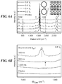
- FIGS. 6A-6D show Raman spectra obtained from an aligned network of SWCNT under the stated conditions of voltage pulsing.
- FIG. 6A shows Raman spectra of pristine SWCNT and SWCNT transformed by 3000 cycles of the indicated voltage pulses. The order of the voltage conditions shown at the upper left is the same as the order of the spectra, from bottom to top. The signature peaks, including radial breathing mode, G, D, and G′, are labeled on the figure.
- CCM coalescence-induced mode
- FIG. 6C shows Raman spectra after 3000 cycles with variation of V a as indicated; the CIM was found at 0.8V b .
- FIG. 6D shows Raman spectra of material obtained after the indicated number of cycles at 0.8V b .
- FIG. 6E shows a plot of the size of the CIM peak as a function of the number of voltage cycles; the peak was at 1500 cycles. Error bars show standard deviation.
- FIG. 6F shows the evolution of the G′ peak as a function of V a .
- FIGS. 7A-7D show electrical and thermal properties of the allotropic carbon forms produced by the method of the invention.
- FIG. 7A shows the in situ two-terminal electrical resistance of SWCNT devices as a function of the indicated number of voltage pulse cycles and V a .
- FIG. 7B shows the ratio of the integrated areas under the D and G bands for the indicated V a values from Raman spectra obtained before and after 3000 voltage pulse cycles.
- FIG. 7C shows the percentage device resistance drop after voltage pulse cycling at 0.8V b for the indicated source on times. The resistance drop was largest when the source on time was smallest.
- FIG. 7D shows the normalized resistance change (contact resistance subtracted, circles) as well as the thermal conductivity (squares) as a function of V a .
- FIGS. 8A-8D show evidence for the emergence of sp 3 structure.
- FIG. 8A shows a scanning electron microscope image of a nanocarbon array transformed after 3000 cycles of 0.8V b (scale bar 200 nm).
- FIG. 8B shows high magnification TEM image (scale bar 1 nm) showing a lattice structure consistent with sp 2 carbon; the inset shows the fast Fourier transform pattern.
- FIG. 8C shows the carbon K-edge energy loss spectrum obtained from the center (upper spectrum) and edge (lower spectrum) of the sample shown in FIG. 8A ; the arrow indicates the appearance of sp 3 in the edge spectrum.
- FIG. 8A shows a scanning electron microscope image of a nanocarbon array transformed after 3000 cycles of 0.8V b (scale bar 200 nm).
- FIG. 8B shows high magnification TEM image (scale bar 1 nm) showing a lattice structure consistent with sp 2 carbon; the inset shows the fast Fourier transform pattern.
- FIG. 8D shows the Raman spectra of the pristine SWCNT (circles), the central region of the voltage pulsed material (spectrum with single large peak), and the edge region of the voltage pulsed material (spectrum with two large peaks). The percentage of sp 3 bonds was derived by comparing these spectra.
- the inset shows a red shift in the central region consistent with the formation of multi-layered sp 2 structures, and a 12.4 cm ⁇ 1 blue shift at the edges, corresponding to about 17% sp 3 structures.
- FIGS. 9A and 9B show schematic illustrations of materials that can be fabricated using methods of the invention.
- FIG. 9A shows a composite material containing an matrix in which a two-dimensional network of interconnected nanocarbon material is embedded.
- FIG. 9B shows two-dimensional graphene sheets connected in the third dimension by aligned carbon nanotube networks.
- the present invention provides new carbon nanomaterials and methods for their fabrication.
- the materials are derived from aligned single-walled carbon nanotube (SWCNT) networks and are prepared using cyclical pulses of alternating voltage and mild heating conditions.
- the methods result in allotropic transformations across the carbon nanotube networks (i.e., from electrode to electrode) to form bundles of aligned SWCNT, enlarged diameter SWCNT, multi-walled carbon nanotubes (MWCNT), or multi-layered graphene nanoribbons (MGNR), or mixtures thereof.
- the transformation process can be controlled by electrical parameters including the amplitude, number of cycles, and duty cycle (on and off times) of alternating voltage pulses. Both open and seamless structures can be formed, and the frequency of structural defects is not increased during the transformational process.
- the invention also provides new materials for use in nanocircuits and microcircuits as well as new composite materials having superior electrical and thermal conductivity and new devices containing the materials.
- Carbon nanotubes naturally align themselves into ropes bound only by van der Waals interactions, and these weak interactions limits their electrical and thermal conductivity in carbon nanotube networks.
- Connecting carbon nanotubes and constructing nanotube junctions with covalent bonds would significantly improve the physical properties of carbon nanotube films.
- Connecting of carbon nanotubes in a controlled manner also offers a promising approach for the bottom-up engineering of nanotube structures.
- the present invention produces new carbon structures by the controlled use of electrical power and the electron migration process. Morphology of small bundled SWCNT changes gradually into larger bundled SWCNT, MWCNT, and MGNR as the time of alternating voltage pulses is increased.
- the MGNR become the dominant form of carbon, as observed by high-resolution transmission electron microscopy (HRTEM).
- HRTEM transmission electron microscopy
- SWCNT or MWCNT can be modified simply into desired nanostructures directly in devices during their fabrication.
- FIG. 1 illustrates how SWCNT are progressively converted to MGNR under appropriate conditions of voltage, voltage cycling, and temperature.
- the initial SWCNT network is initially composed of individual SWCNT non-covalently associated by van der Waals interactions.
- these SWCNT are converted to small bundles of SWCNT (see section “a” of FIG. 1 ), having a few SWCNT (e.g., 2, 3, 4, 5, 6, 7, 8, or 9 SWCNT) arranged in parallel along their axis and in close contact.
- Further energy input e.g., higher applied voltage, V a , during voltage pulse cycles
- leads to the formation of large bundles of SWCNT see section “b” of FIG.
- FIGS. 2A-2F show SEM and TEM images of the SWCNT, MWCNT, and MGNR structures formed by this process.
- the allotropic transformation process of the invention starts with a network, array, or bundle of aligned carbon nanotube material, such as SWCNT, MWCNT, or carbon nanotube fibers (also referred to herein as “SWCNT or MWCNT network”) disposed across a gap between two electrodes and in electrical contact with the electrodes.
- the carbon nanotube material can be transferred onto a nonconductive substrate material, such as silicon, silicon dioxide, or a non-conductive polymer material, for example.
- the electrodes can be metal layers, e.g., patterned by lithography, deposited on the substrate material.
- the SWCNT or MWCNT network and electrodes can optionally be part of a nanocircuit or microcircuit including additional components added either before or after the allotropic transformation of the SWCNT.
- the electrodes and the SWCNT or MWCNT network can have any form desired, such as rectangular, square, circular, or irregular.
- the SWCNT or MWCNT network and electrodes are two-dimensional shapes laid out on a plan
- the aligned SWCNT or MWCNT network can be prepared by any known technique for assembling, depositing, and/or aligning carbon nanotube materials.
- a preferred technique is template-guided fluidic assembly (30-32), but other methods can be used, such as assembly by electrophoresis and/or dielectrophoresis.
- the network should have a high density that permits and promotes lateral interactions among neighboring nanotubes.
- the density of the SWCNT or MWCNT network can be 5000, 10000, 15000, 20000, 25000, 30000, 35000, or 40000 or more SWCNT or MWCNT per ⁇ m 2 (square micron).
- a preferred density is 15000-25000 SWCNT or MWCNT per ⁇ m 2 .
- a more preferred density is 18000-22000, or about 20000 SWCNT or MWCNT per ⁇ m 2 or higher.
- FIG. 3 presents an SEM image of a specially fabricated device that allowed for TEM observation of the allotropic transformation process.
- Well-defined SWCNT microlines were directly assembled on specially designed TEM grids where microwindows were located between built-in micro-heaters for external heating.
- the device 10 shown in FIG. 4A includes an assembled SWCNT network microline 30 between two electrodes 20 ; the SWCNT network and electrodes are disposed on insulating substrate 40 .
- initial I-V characterization was performed to find the maximum current density (J b ) and the breakdown voltage (V b ) of assembled SWCNT networks under vacuum ( FIG. 4B ).
- FIG. 4C shows the time-dependent alternating voltage pulses applied to the SWCNT networks.
- the electrical polarity was switched periodically (typically at 1 Hz for 3,000 cycles) for several applied voltage amplitudes (V a , FIG. 4C ) ranging from 0.4V b to 0.8V b , where the I-V curves turn slightly nonlinear ( FIG. 4B ) because of increased electron-phonon scattering and structural changes (33).
- the source-on-time (t on in FIG. 4C ) for each V a was also varied to obtain the most effective transformation conditions.
- FIG. 5A shows a typical TEM image of the pristine SWCNT network (before electrical treatment) containing individual and bundles of SWCNT.
- FIG. 5B-F show TEM images showing representative results after the cycling steps were completed using the indicated values of V a .
- Two different regimes were observed as the V a was increased. One is from 0 to 0.4V b , where I versus V is linear and in which no significant structural changes occur. The other regime is from 0.4V b to 0.8V b , where structural changes in the nanotube array take place along with active rearrangement of carbon atoms. Three different sp 2 carbon nanostructures were predominantly observed at the applied voltages of 0.6V b and 0.8V b .
- Raman spectroscopy measurements were performed at the same location in the SWCNT network before and after subjecting the sample to various voltages from 0.2V b to 0.8V b .
- Shown in FIG. 6A are overall Raman spectra showing four representative Raman features: the radial breathing mode, the D-band, the G-band and the G′-band, each representing unique spectral evolutions, not previously observed, as the applied voltage was increased.
- the expected location of a fifth emergent feature, the CIM (13,38-40) is indicated with a dashed rectangle.
- the CIMs provide a confirmation that carbon atoms in the nanotube lattice are migrating to form different sp 2 carbon structures that are mediated via the temporary appearance of junctions in the form of linear C-chains between adjacent nanotubes (13,38-40) as shown schematically in the inset of FIG. 6A . These modes have been determined to be a precursor to the coalescence process in high-temperature-induced coalescence of nanotubes (38).
- FIG. 6B shows typical Raman spectra near the CIM mode for samples that have been cycled using different on times, t on (keeping t off constant at 400 ms).
- t on 500 ms
- t on 100 ms.
- the disappearance of CIM modes for larger t on values implies that rapid switching of the voltage pulse is a more effective method to obtain the transformations.
- FIG. 6F shows the line-shape and intensity change in the G′-band spectra after electrical treatment with different applied voltages.
- the average peak position of the G′-band is known to red-shift to lower frequencies with increasing mean nanotube diameter (41).
- the clear emergence of a red-shifted peak centered around 2,625 cm ⁇ 1 was observed after voltage cycling, consistent with the coalescence of small diameter SWCNT, which forms bigger diameter SWNT/MWNT, and the collapse of MWCNT into their layer-stacked MGNR counterparts.
- FIG. 7A shows the resistance change as a function of the number of cycles at alternating voltage pulses of 0.4V b , 0.6V b and 0.8V b , respectively.
- V a 0.4V b
- the electrical resistance was seen to increase slowly over time over the entire cycling period. Since neither TEM nor Raman investigations indicated any structural transformations at this V a value, and analysis of the D-band of Raman spectrum ( FIG.
- FIG. 7B shows the variation of IA D /IA G (ratio of the integrated areas of the D and G bands) as a function of V b .
- the electrical resistance drop was found to be largest when the duty-cycle was smallest, which is in direct agreement with the t on -dependent appearance of the CIM ( FIG. 6B ), suggesting that rapid pulse-switching (when t on is small) rather than prolonged Joule-heating (when t on is large) better assists in the transformation processes.
- FIG. 8A shows an SEM image of the network structure after being cycled at 0.8V b .
- High-resolution TEM image of the central portion of this structure ( FIG. 8B ) reveals that the transformed network consists of a multi-layered graphitic sp2 structure.
- the measured in-plane lattice spacing in the center was 0.24 ⁇ 0.02 nm, which is identical to the sp 2 carbon structure (24).
- carbon K-edge energy loss spectrum (EELS) and resonant Raman spectroscopy results that compare the central region versus the edges of these networks revealed that at the edges the network was transformed to sp 2 -sp 3 hybrid nanostructures.
- EELS carbon K-edge energy loss spectrum
- Raman spectroscopy results that compare the central region versus the edges of these networks revealed that at the edges the network was transformed to sp 2 -sp 3 hybrid nanostructures.
- the EELS spectra from the center and the edge regions of the sample shown in FIG. 8A are compared.
- sp 2 bonds exhibit a peak around 290 eV because of s* states and the other peak appears at 285 eV corresponding to p* states (42-44), as seen in the spectrum measured from the center of the sample.
- the EELS spectrum measured at the edges shows clear signatures of sp 3 -type carbon: a s* edge around 290 eV corresponding to the sp 3 transition 1s-2s* (45) and a dip around 302 eV that corresponds to the second absolute band gap characteristic of the crystalline sp 3 structure (46,47).
- the sp 2 carbon band at about 285 eV became a very shallow shoulder in the spectrum of the sp 3 -bonded carbon.
- the relative G-band shift in Raman spectra focused on two different locations, center and edges of the transformed network ( FIG. 8D ), was used to estimate the percentage abundance of sp 3 carbon.
- the Raman spectra, taken at the center of networks, zoomed into the G-band range (inset in FIG. 8D ) indicate that this transformed network kept mostly crystalline sp 2 bonds.
- Raman spectrum shows the characteristics of a nanocrystallization of the pristine material with highly disordered sp 2 bonds (amorphization) and the rise of some sp 3 bonds.
- the first is Joule heating.
- the transformations are more effective under rapid voltage-switching (smaller values of t on ) rather than higher heat-generating (larger values of t on ) cycles. This indicates that Joule heating alone is not sufficient to explain the transformation process.
- the nanoscale forces that initially align the nanotubes bring them to van der Waals proximities. Thermal fluctuations and electromigration may cause these atoms to move out of their lattice sites, and these mobile atoms minimize their energies by forming linear chains between two SWNCTs ( FIG. 6A ) that forms a junction between nanotubes and gives rise to the CIMs in Raman spectroscopy. With continued cycling, the junction grows wider and eventually becomes comparable in size with the nanotube diameters and the nanotubes release mechanical strain by coalescing into larger-diameter structures.
- the engineered carbon structures that can be produced with the present invention allow the full electrical and thermal conductivity of graphene to be realized for use in interconnects for high speed nanoscale electronics and nanomechanical devices.
- One method of preparing an SWCNT network suitable as starting material for a method of the invention is described by way of example.
- these template substrates were dip-coated in a 0.23 wt % high-purified SWCNT solution at a constant pulling rate of 0.1 mm/min.
- the dip-coating processes result in stable and densely aligned SWCNT lateral network architectures on the substrate having well-defined shapes at the nanoscale.
- the photoresist was removed to obtain well-organized and aligned SWCNT lateral networks.
- the SWCNT density in the network array was estimated as follows.
- the networks made from dip-coating techniques typically have small surface roughness and close-packing structures with 80% dense SWCNT.
- the cross-sectional area is approximately 18,000 nm 2 ⁇ 3,000 nm 2 . Therefore, the number of SWCNT in the network of 2 mm 2 dimension is calculated as about (4 ⁇ 0.5)10 4 ((2 ⁇ 0.25)10 12 cm ⁇ 2 ).
- a Keithley 2,400 sourcemeter was used to apply voltage and to measure the resistance across the two terminal SWCNT devices. All the measurements were done under high vacuum (P ⁇ 10 ⁇ 5 Torr) in a Janis Research ST-500 cryogenic probe station to reduce radial heat losses through gas convection and to avoid burning the devices. Voltage sweeps were applied through SWCNT arrays to find the breakdown voltage. Most of the arrays failed at a maximum current density of about 4.3 ⁇ 10 7 A/cm 2 , and the breakdown voltage (V b ) was 2.7V on the TEM window ( FIG. 4B ). By sweeping the voltage over a suitable range, a critical voltage was observed for which the graphitization process was accelerated. At the same time, applied voltages too close to V b often led to the breakdown of the nanotube. Therefore, V b for these quasiparallel SWCNT networks was found to be an important parameter.
- I 1v [mA] is the current at 1 V.
- Arrays with a nearly similar current density were used for testing the reproducibility of the transformation process.
- repetitive positive and negative voltages of 0.4V b , 0.6V b and 0.8V b for which the electrical powers were in the range of 2-3, 6-8 and 10-15 mW, respectively, under the employed device condition (for SiO2-coated Si substrate), were each applied at 1 Hz for 3,000 cycles at 180° C. (453 K) between the two electrodes on the SWCNT arrays.
- Breakdown occurs when the maximum temperature of the tube reaches the value of the breakdown temperature, which allows the extraction of a simple expression for the breakdown voltage of SWCNTs, including heat generation from Joule self-heating and heat loss to the substrate (50,51).
- T BD is the maximum temperature
- P BD is the breakdown power
- R C is estimated from the inverse slope of the low-bias I D ⁇ V SD plot
- g is the heat dissipation coefficient in the substrate per unit length
- L is length of SWCNT network. From the equation, the calculated maximum temperature is about 1,335 K (1,062 C). At 0.8V b ,
- the SWCNT arrays were prepared on specially designed chips with a window of 40 ⁇ 40 ⁇ m 2 for SEM and TEM imaging.
- the SWCNT arrays were suspended on an electron transparent window by employing a two-probe device architecture.
- Two micro-heater electrodes of 10 ⁇ m in width were employed around the arrays on the chip for the external heating.
- the TEM measurements were carried out in a JEOL-3011 high-resolution TEM instrument using an accelerating voltage of 300 kV. The allotropes covered a significant area of the devices, which was verified by taking TEM images at different positions over the sample.
- Raman spectroscopy (LabRAM HR 800, HORIBA Jobin Yvon, HORIBA) was used to investigate structure changes of SWCNT arrays as the applied voltage and the numbers of cycles were changed.
- the laser excitation wavelengths used were 532 nm (2.33 eV) and 633 nm (1.92 eV), the exposure time was 5 s per spectrum, and the number of data accumulations was 10.
- a 600 line per mm grating was used, and the confocal hole diameter was set to 100 ⁇ m.
- the contact resistance was measured in all test structures, which had a lateral width of 1 ⁇ m.
- the four contact pads were separated by a distance of 2 ⁇ m from each other. I-V measurements were conducted between the pairs of contacts A-B, B-C, C-D, A-C, and B-D.
- the resistance R d BC is defined as a device resistance between contact pads B and C. Therefore, the two contact resistances and the resistances of the SWCNT array itself were all calculated from data taken on five pairs of device resistances and the values were compared before and after the SWCNT array treatment.
- the measurement of thermal conductivity was performed by using a self-heating 3 ⁇ technique (53,54).
- the 3 ⁇ signal correlates with the thermal conductivity through the following equation (53,54):
- V 3 ⁇ ,rms (4 I 3 RR′L )/ ⁇ 4 kS
- L, R and S are the distances between the contacts, the electrical resistance and the cross-sectional area of the sample, respectively,
- the 3 ⁇ method was used by the four-point-probe third harmonic characterization method to eliminate the contact resistance and to avoid related spurious signals.
- the 3 ⁇ signals were used for measuring the thermal conductivity of the SWCNT arrays.
- a lock-in amplifier (Stanford Research System SR850) was used for obtaining the 3 ⁇ signals by amplifying the small voltage and removing the noise.
- An AC current source (Keithley 6221) was used to provide a stable current supply. All the measurements including the resistance, temperature, and 3 ⁇ signals were done under high vacuum (P ⁇ 10 ⁇ 5 Torr) in a Janis Research ST-500 cryogenic probe station to reduce radial heat losses through gas convection. The temperature coefficient of the resistance should be measured in order to obtain the thermal conductivity based on the above equation.
- the resistance-temperature coefficient of the SWCNT arrays themselves was also measured over the small temperature range of 296-300 K, which is close to the measurement temperature of the 3 ⁇ signal.
- the resistance change of the pristine SWCNT as a function of temperature was about 53.7 ⁇ K ⁇ 1 .
- Those of the samples treated at 0.4V b and 0.6V b showed a negative resistance temperature (R(T)) value of ⁇ 26.2 ⁇ K ⁇ 1 and ⁇ 9.03 ⁇ K ⁇ 1 , respectively.
- R(T) showed a positive value of 1.6 ⁇ K ⁇ 1 for the sample treated at 0.8V b .
- the exponent of the current amplitude I 0 was found to be 2.8-3.1 for the samples. These values are very close to the third power predicted from theory.
- the calculated thermal conductivities were 58.5, 63.5, 13.1 and 301.2 W mK ⁇ 1 for the pristine SWCNT, and samples treated at 0.4V b , 0.6V b and 0.8V b , respectively ( FIG. 7D ).
- the factor of five increase of the effective thermal conductivity in the array treated at 0.8V b is believed to be caused by the highly reduced junction scattering and the thermal pathways to sp 3 structures.
Landscapes
- Chemical & Material Sciences (AREA)
- Organic Chemistry (AREA)
- Engineering & Computer Science (AREA)
- Nanotechnology (AREA)
- Materials Engineering (AREA)
- Inorganic Chemistry (AREA)
- Health & Medical Sciences (AREA)
- General Health & Medical Sciences (AREA)
- Toxicology (AREA)
- Chemical Kinetics & Catalysis (AREA)
- Carbon And Carbon Compounds (AREA)
Abstract
Description
- 1. A method for allotropic transformation of a carbon nanotube material, the method comprising the steps of:
- 2. The method of
item 1, wherein 1000≤n≤3000. - 3. The method of
item - 4. The method of any of the previous items, wherein the polarity of Va is switched at a frequency of from about 0.1 to about 200 Hz.
- 5. The method of any of the previous items, wherein the polarity of Va is switched at a frequency of about 100 Hz.
- 6. The method of any of the previous items, wherein Va is applied as a series of DC pulses, and wherein each pulse is applied for a period of from about 2 msec to about 1000 msec.
- 7. The method of any of the previous items, wherein each cycle consists of a positive pulse of amplitude Va, a negative pulse of amplitude −Va, and periods between the pulses where Va=0.
- 8. The method of any of the previous items, wherein the positive and negative pulses last for about 10% of the cycle.
- 9. The method of any of the previous items, wherein the carbon nanotube material comprises single walled carbon nanotubes (SWCNT), multiwalled carbon nanotubes (MWCNT), or carbon nanotube fiber.
- 10. The method of any of the previous items, wherein the SWCNT, MWCNT, or carbon nanotube fibers are aligned along an axis extending between the electrodes.
- 11. The method of any of the previous items, wherein the carbon nanotube material comprises carbon nanotubes at a density of about 18,000-22,000 SWCNT per μm2.
- 12. The method of any of the previous items, wherein the carbon nanotube material comprises SWCNT and the allotropic transformation produces an increase in SWCNT diameter of about 30% to about 40%.
- 13. The method of any of the previous items, wherein the carbon nanotube material comprises SWCNT and the allotropic transformation produces small bundles of SWCNT having less than 10 SWCNT per bundle.
- 14. The method of any of the previous items, wherein the carbon nanotube material comprises SWCNT and the allotropic transformation produces large bundles of SWCNT having 10 or more SWCNT per bundle.
- 15. The method of any of the previous items, wherein Va is about 0.6Vb.
- 16. The method of any of the previous items, wherein the carbon nanotube material comprises SWCNT and the allotropic transformation produces multiwalled carbon nanotubes (MWCNT).
- 17. The method of any of the previous items, wherein the MWCNT have diameters in the range from about 15 nm to about 30 nm.
- 18. The method of any of the previous items, wherein some of the MWCNT have incomplete outer wall structure.
- 19. The method of any of the previous items, wherein the MWCNT have essentially complete outer wall structure.
- 20. The method of any of the previous items, wherein Va is from about 0.6Vb to about 0.8Vb.
- 21. The method of any of the previous items, wherein the allotropic transformation produces multilayered graphene nanoribbons (MGNR).
- 22. The method of any of the previous items, wherein at least some of the MGNR are in the form of flattened stacks.
- 23. The method of any of the previous items, wherein at least some of the MGNR are in the form of closed end structures.
- 24. The method of any of the previous items, wherein at least some of the MGNR are in the form of open end structures.
- 25. The method of any of the previous items, wherein Va is about 0.8Vb.
- 26. The method of any of the previous items, wherein the allotropic transformation produces multilayered graphitic nanoribbons (MGNR).
- 27. The method of any of the previous items, wherein the carbon nanotube material comprises SWCNT.
- 28. The method of any of the previous items, wherein the carbon nanotube material consists of SWCNT.
- 29. The method of any of the previous items, wherein the carbon nanotube material comprises MWCNT.
- 30. The method of any of the previous items, wherein the carbon nanotube material consists of MWCNT.
- 31. The method of any of the previous items, wherein the carbon nanotube material comprises carbon nanotube fibers.
- 32. The method of any of the previous items, wherein the carbon nanotube material consists of carbon nanotube fibers.
- 33. The method of any of the previous items, wherein carbon-carbon sp2 bonds of the carbon nanotube material are rearranged and coalescence-induced modes increase in Raman spectra of the material.
- 34. The method of any of the previous items, wherein some sp2 bonds in the carbon nanotube material are converted to sp3 bonds.
- 35. The method of any of the previous items, wherein steps (b) and (c) are performed at a temperature in the range from about 120° C. to about 400° C.
- 36. The method of any of the previous items, wherein steps (b) and (c) are performed at a temperature of about 180° C.
- 37. The method of any of the previous items, wherein the method is performed at a temperature below 200° C.
- 38. The method of any of the previous items, wherein steps (b) and (c) are performed in a vacuum.
- 39. The method of any of the previous items, wherein the carbon nanotube material and two electrodes are part of a circuit on a chip, and said method is part of a manufacturing process for the chip.
- 40. The method of any of the previous items, wherein structural defects initially present in the carbon nanotube material are reduced.
- 41. The method of any of the previous items, wherein the allotropic transformation progresses from forming MWCNT to forming MGNR as the number of voltage cycles increases.
- 42. The method of any of the previous items, wherein the number of voltage cycles is selected so as to produce a desired allotropic form or mixture of allotropic forms of carbon material.
- 43. The method of any of the previous items, wherein at least 50% of the initial carbon nanotube material is transformed into a different allotropic form.
- 44. The method of any of the previous items, wherein at least 90% of the initial carbon nanotube material is transformed into a different allotropic form.
- 45. The method of any of the previous items, wherein essentially all of the initial carbon nanotube material is transformed into a different allotropic form.
- 46. The method of any of the previous items, wherein essentially all of the initial carbon nanotube material is transformed into MGNR.
- 47. A multilayered graphene nanoribbon (MGNR) carbon material produced by the method of any of the previous items.
- 48. A circuit comprising the MGNR material of item 47.
- 49. A composite structural material comprising the MGNR material of item 47.
- 50. An electronic device comprising a network of multilayered graphene nanoribbons, the network bridging a gap between two electrodes and in electrical contact with each of the two electrodes.
- 51. An MGNR material having a thermal conductivity of at least 250 W mK−1.
sp 3(%))=0.24-0.0049*(ωG(edge)−ωG(center)),
in which ωG(edge)=1,602.4 cm−1 and ωG(center)=1,590 cm−1 stand for the G-mode Raman frequency at the edges and in the center of the resultant material. According to this expression, there are about 17% of sp3 bonds at the edges (as annotated in
V BD =gL(T BD −T 0)/I BD +I BD R C
Therefore, the maximum temperature at the breakdown voltage is:
T BD=(P BD −I 2 BD R C)/gL+T 0
Here, TBD is the maximum temperature, PBD is the breakdown power, the combined resistance of the source and drain contacts, RC is estimated from the inverse slope of the low-bias ID−VSD plot, RC≈(dID/dVSD)−1, g is the heat dissipation coefficient in the substrate per unit length and L is length of SWCNT network. From the equation, the calculated maximum temperature is about 1,335 K (1,062 C). At 0.8Vb, the temperature is calculated as about 1,200 K.
R c B=(R AB +R BC −R AC)/2
R c C=(R BC +R CD −R BD)/2
where RAB=Rc A+Rd AB+Rc B, RBC=Rc B+Rd BC+Rc C, RAC=Rc A+Rd AC+Rc C, RCD=Rc C+Rd CD+Rc D, and RBD=Rc B+Rd BD+RC D. The resistance Rd BC is defined as a device resistance between contact pads B and C. Therefore, the two contact resistances and the resistances of the SWCNT array itself were all calculated from data taken on five pairs of device resistances and the values were compared before and after the SWCNT array treatment.
V 3ω,rms=(4I 3 RR′L)/π4 kS
where L, R and S are the distances between the contacts, the electrical resistance and the cross-sectional area of the sample, respectively, R′=(δR/δT) is the temperature gradient of the resistance at the chosen temperature and k is the thermal conductivity. The 3ω method was used by the four-point-probe third harmonic characterization method to eliminate the contact resistance and to avoid related spurious signals.
- 1. Volder, M., Tawfick, S., Baughman, R. H. & Hart, A. J. Carbon nanotubes: present and future commercial applications. Science 339, 535-539 (2013).
- 2. Cao, Q. et al. Arrays of single-walled carbon nanotubes with full surface coverage for high-performance electronics. Nat. Nanotech. 8, 180-186 (2013).
- 3. Zhang, X. et al. Ultrastrong, stiff and lightweight carbon-nanotube fibers. Adv. Mater. 19, 4198-4201 (2007).
- 4. Lin, H. et al. Conducting polymer composite film incorporated with aligned carbon nanotubes for transparent, flexible and efficient supercapacitor. Sci. Rep. 3, 1353 (2013).
- 5. Srivastava, A. et al. Carbon nanotube filters. Nat. Mater. 3, 610-614 (2004).
- 6. Wu, Y. et al. Conformal Fe3O4 sheath on aligned carbon nanotube scaffolds as high-performance anodes for lithium ion batteries. Nano Lett. 13, 818-823 (2013).
- 7. Vilatela, J. J., Elliott, J. A. & Windle, A. H. A model for the strength of yarn-like carbon nanotube fibers.
ACS Nano 5, 1921-1927 (2011). - 8. Hirsch, A. The era of carbon allotropes. Nat. Mater. 9, 868-871 (2010).
- 9. Jiao, L. et al. Narrow graphene nanoribbons from carbon nanotubes. Nature 458, 877-880 (2009).
- 10. Hu, M. et al. Compressed carbon nanotubes: a family of new multifunctional carbon allotropes. Sci. Rep. 3, 1331 (2013).
- 11. Krasheninnikov, A. V. & Banhart, F. Engineering of nanostructured carbon materials with electron or ion beams. Nat. Mater. 6, 723-733 (2007).
- 12. Wei, D. & Liu, Y. The intramolecular junctions of carbon nanotubes. Adv. Mater. 20, 2815-2841 (2008).
- 13. Endo, M. et al. Coalescence of double-walled carbon nanotubes: formation of novel carbon bicables. Nano Lett. 4, 1451-1454 (2004).
- 14. Terrones, M. et al. Molecular junctions by joining single-walled carbon nanotubes. Phys. Rev. Lett. 89, 0755051-0755054 (2002).
- 15. Yao, Z., Postma, H. W. C., Balents, L. & Dekker, C. Carbon nanotube intramolecular junctions. Nature 402, 273-276 (1999).
- 16. Papadopoulos, C. et al. Electronic transport in Y-junction carbon nanotubes. Phys. Rev. Lett. 85, 3476-3479 (2000).
- 17. Zhou, C. W., Kong, J., Yenilmez, E. & Dai, H. J. Modulated chemical doping of individual carbon nanotubes.
Science 290, 1552-1555 (2000). - 18. Bandaru, P. R., Daraio, C., Jin, S. & Rao, A. M. Novel electrical switching behaviour and logic in carbon nanotube Y-junctions. Nat. Mater. 4, 663-666 (2005).
- 19. Kis, A. et al. Reinforcement of single-walled carbon nanotube bundles by intertube bridging. Nat. Mater. 3, 153-157 (2004).
- 20. Terrones, M. et al. Coalescence of single-walled carbon nanotubes. Science 288, 1226-1229 (2000).
- 21. Li, J. & Banhart, F. The engineering of hot carbon nanotubes with a focused electron beam. Nano Lett. 4, 1143-1146 (2004).
- 22. Yao, Y. et al. Temperature-mediated growth of single-walled carbon-nanotube intramolecular junctions. Nat. Mater. 6, 283-286 (2007).
- 23. Collins, P. G., Arnold, M. S. & Avouris, P. Engineering carbon nanotubes and nanotube circuits using electrical breakdown. Science 292, 706-709 (2001).
- 24. Jia, X. et al. Controlled formation of sharp zigzag and armchair edges in graphitic nanoribbons. Science 323, 1701-1705 (2009).
- 25. Jin, C., Suenaga, K. & Iijima, S. Plumbing carbon nanotubes. Nat. Nanotech. 3, 17-21 (2008).
- 26. Yuzvinsky, T. D. et al. Shrinking a carbon nanotube. Nano Lett. 6, 2718-2722 (2006).
- 27. Mølhave, K. et al. Transmission electron microscopy study of individual carbon nanotube breakdown caused by joule heating in air. Nano Lett. 6, 1663-1668 (2006).
- 28. Gutierrez, H. R., Kim, U. J., Kim, J. P. & Eklund, P. C. Thermal conversion of bundled carbon nanotubes into graphitic ribbons. Nano Lett. 5, 2195-2201 (2005).
- 29. Romo-Herrera, J. M. et al. Covalent 2D and 3D networks from 1D nanostructures: Designing new materials. Nano Lett. 7, 570-576 (2007).
- 30. Jaber-Ansari, L. et al. Mechanism of very large scale assembly of SWNTs in template guided fluidic assembly process. J. Am. Chem. Soc. 131, 804-808 (2009).
- 31. Xiong, X. et al. Building highly organized single-walled carbon nanotube networks using template guided fluidic assembly. Small 3, 2006-2010 (2007).
- 32. Somu, S. et al. Topological transition in carbon nanotube networks via nanoscale confinement. ACS Nano 4, 4142-4148 (2010).
- 33. Yao, Z., Kane, C. L. & Dekker, C. High-field electrical transport in single-wall carbon nanotubes. Phys. Rev. Lett. 84, 2941-2944 (2004).
- 34. Yoon, M. et al. Zipper mechanism of nanotube fusion: theory and experiment. Phys. Rev. Lett. 92, 0755041-0755044 (2004).
- 35. Ajayan, P. M., Ravikumar, V. & Charlier, J.-C. Surface reconstructions and dimensional changes in single-walled carbon nanotubes. Phys. Rev. Lett. 81, 1437-1440 (1998).
- 36. Hernandez, E. et al. Fullerene coalescence in nanopeapods: a path to novel tubular carbon. Nano Lett. 3, 1037-1042 (2003).
- 37. Endo, M. et al. Atomic nanotube welders: boron interstitials triggering connections in double-walled carbon nanotubes. Nano Lett. 5, 1099-1105 (2005).
- 38. Endo, M. et al. Nanotube coalescence-inducing mode: a novel vibrational mode in carbon systems. Small 2, 1031-1036 (2006).
- 39. Fantini, C. et al. Resonance Raman study of linear carbon chains formed by the heat treatment of double-wall carbon nanotubes. Phys. Rev. B 73, 1934081-1934084 (2006).
- 40. Villalpando-Paez, F. et al. Raman spectroscopy study of heat-treated and boron-doped double wall carbon nanotubes. Phys. Rev. B 80, 0354191-03541914 (2009).
- 41. Filho, S. et al. Competing spring constant versus double resonance effects on the properties of dispersive modes in isolated single-wall carbon nanotubes. Phys. Rev. B 67, 035427-035434 (2003).
- 42. Papworth, A. P. et al. Electron-energy-loss spectroscopy characterization of the sp2 bonding fraction within carbon thin films. Phys. Rev. B 62, 12628-12631 (2000).
- 43. Okada, K., Kimoto, K., Komatsu, S. & Matsumoto, S. Sp2 bonding distributions in nanocrystalline diamond particles by electron energy loss spectroscopy. J. Appl. Phys. 93, 3120-3122 (2003).
- 44. Castrucci, P. et al. Probing the electronic structure of carbon nanotubes by nanoscale spectroscopy. Nanoscale 2, 1611-1625 (2010).
- 45. Prawer, S. et al. The Raman spectrum of nanocrystalline diamond. Chem. Phys. Lett. 332, 93-97 (2000).
- 46. Mykhaylyka, O. O., Solonin, Y. M., Batchelder, D. N. & Brydson., R. Transformation of nanodiamond into carbon onion. J. Appl. Phys. 97, 074302-074315 (2005).
- 47. Arenal, R. et al. Diamond nanowires and the insulator-metal transition in ultrananocrystalline diamond films. Phys. Rev. B 75, 195431-11 (2007).
- 48. Singha, A., Ghosh, A., Roy, A. & Ray, N. R. Quantitative analysis of hydrogenated diamondlike carbon films by visible Raman spectroscopy. J. Appl. Phys. 100, 044910 (2006).
- 49. Sorbello, R. Theory of electromigration. Solid State Phys. 51, 159-231 (1997).
- 50. Pop, E., Mann, E. A., Goodson, K. E. & Dai, H. Electrical and thermal transport in metallic single-wall carbon nanotubes on insulating substrates. J. Appl. Phys. 101, 093710 (2007).
- 51. Liao, A. et al. Thermal dissipation and variability in electrical breakdown of carbon nanotube devices. Phys. Rev. B 82, 205406 (2010).
- 52. Kim, Y. L. et al. Highly aligned scalable platinum-decorated single-wall carbon nanotube arrays for nanoscale electrical interconnects.
ACS Nano 3, 2818-2826 (2009). - 53. Li, B. et al. Ultra-thin SWNTs films with tunable, anisotropic transport properties. Adv. Funct. Mater. 21, 1810-1815 (2011).
- 54. Choi, T., Poulikakos, D., Tharian, J. & Sennhauser, U. Measurement of the thermal conductivity of individual carbon nanotubes by the four-point three-w method. Nano Lett. 6, 1589-1593 (2006).
Claims (17)
Priority Applications (1)
| Application Number | Priority Date | Filing Date | Title |
|---|---|---|---|
| US15/510,789 US10646846B2 (en) | 2014-09-12 | 2015-09-14 | Fabrication of carbon nanoribbons from carbon nanotube arrays |
Applications Claiming Priority (3)
| Application Number | Priority Date | Filing Date | Title |
|---|---|---|---|
| US201462049440P | 2014-09-12 | 2014-09-12 | |
| PCT/US2015/050002 WO2016040948A1 (en) | 2014-09-12 | 2015-09-14 | Fabrication of carbon nanoribbons from carbon nanotube arrays |
| US15/510,789 US10646846B2 (en) | 2014-09-12 | 2015-09-14 | Fabrication of carbon nanoribbons from carbon nanotube arrays |
Publications (2)
| Publication Number | Publication Date |
|---|---|
| US20170247257A1 US20170247257A1 (en) | 2017-08-31 |
| US10646846B2 true US10646846B2 (en) | 2020-05-12 |
Family
ID=55459658
Family Applications (1)
| Application Number | Title | Priority Date | Filing Date |
|---|---|---|---|
| US15/510,789 Active 2037-03-21 US10646846B2 (en) | 2014-09-12 | 2015-09-14 | Fabrication of carbon nanoribbons from carbon nanotube arrays |
Country Status (3)
| Country | Link |
|---|---|
| US (1) | US10646846B2 (en) |
| EP (1) | EP3191300A1 (en) |
| WO (1) | WO2016040948A1 (en) |
Families Citing this family (7)
| Publication number | Priority date | Publication date | Assignee | Title |
|---|---|---|---|---|
| WO2018169889A1 (en) | 2017-03-16 | 2018-09-20 | Lyten, Inc. | Carbon and elastomer integration |
| US10920035B2 (en) | 2017-03-16 | 2021-02-16 | Lyten, Inc. | Tuning deformation hysteresis in tires using graphene |
| US9862606B1 (en) | 2017-03-27 | 2018-01-09 | Lyten, Inc. | Carbon allotropes |
| US11479467B2 (en) * | 2018-01-10 | 2022-10-25 | Lawrence Livermore National Security, Llc | Covalent reinforcement of carbon nanotube assemblies |
| WO2020051000A1 (en) * | 2018-09-05 | 2020-03-12 | William Marsh Rice University | Flash joule heating synthesis method and compositions thereof |
| US11760633B2 (en) * | 2020-01-31 | 2023-09-19 | Surgepower Materials Inc. | Method of preparing carbon nanomaterials |
| CN113845416B (en) * | 2020-06-28 | 2023-09-05 | 中国石油化工股份有限公司 | A method for preparing oxygen-containing organic compounds by catalytic oxidation of naphthenes |
Citations (4)
| Publication number | Priority date | Publication date | Assignee | Title |
|---|---|---|---|---|
| US20090226361A1 (en) * | 2008-03-05 | 2009-09-10 | Jessica Campos-Delgado | Cvd-grown graphite nanoribbons |
| US20100142259A1 (en) | 2005-03-21 | 2010-06-10 | The Trustees Of The University Of Pennsylvania | Nanogaps: methods and devices containing same |
| WO2013056182A1 (en) | 2011-10-12 | 2013-04-18 | Devernoe David | Piezoelectric devices and methods |
| US20140127415A1 (en) | 2012-04-05 | 2014-05-08 | Hamid Assadi | Method for manufacturing diamond |
-
2015
- 2015-09-14 US US15/510,789 patent/US10646846B2/en active Active
- 2015-09-14 WO PCT/US2015/050002 patent/WO2016040948A1/en not_active Ceased
- 2015-09-14 EP EP15840342.8A patent/EP3191300A1/en not_active Withdrawn
Patent Citations (4)
| Publication number | Priority date | Publication date | Assignee | Title |
|---|---|---|---|---|
| US20100142259A1 (en) | 2005-03-21 | 2010-06-10 | The Trustees Of The University Of Pennsylvania | Nanogaps: methods and devices containing same |
| US20090226361A1 (en) * | 2008-03-05 | 2009-09-10 | Jessica Campos-Delgado | Cvd-grown graphite nanoribbons |
| WO2013056182A1 (en) | 2011-10-12 | 2013-04-18 | Devernoe David | Piezoelectric devices and methods |
| US20140127415A1 (en) | 2012-04-05 | 2014-05-08 | Hamid Assadi | Method for manufacturing diamond |
Non-Patent Citations (6)
| Title |
|---|
| Gutierrez H et al. Thermal Conversion of Bundled Carbon Nanotubes into Graphitic Ribbons. Nano Letters, vol. 5, No. 11, pp. 2195-22011 (2005). |
| Hu J et al. Thermal Conductivity and Thermal Rectification in Graphene Nanoribbons: A Molecular Dynamics Study. Nano Letters, vol. 9, No. 7, pp. 2730-2735 (2009). |
| Li, et al., Carbon nanomaterials: the ideal interconnect technology for next-generation ICs, IEEE Des. Test Comput.,2010; 27(4): 20-31 (Year: 2010). * |
| Terrones M et al. Coalescence of Single-Walled Carbon Nanotubes. Science May 19, 2000: vol. 288, Issue 5469, pp. 1226-1229. |
| Yao Y et al. Temperature-mediated growth of single-walled carbon-nanotube intramolecular junctions. Nat. Mat. 6, 283-286 (2007). |
| Zhao, et al., Comparative Study of Multilayer Graphene Nanoribbon (MLGNR) Interconnects, IEEE Transactions on Electromagnetic Compatibility 2014; 56(3): 638-645 (Year: 2014). * |
Also Published As
| Publication number | Publication date |
|---|---|
| WO2016040948A1 (en) | 2016-03-17 |
| US20170247257A1 (en) | 2017-08-31 |
| EP3191300A1 (en) | 2017-07-19 |
Similar Documents
| Publication | Publication Date | Title |
|---|---|---|
| US10646846B2 (en) | Fabrication of carbon nanoribbons from carbon nanotube arrays | |
| Kim et al. | Graphene nanoribbons obtained by electrically unwrapping carbon nanotubes | |
| Zhu et al. | Growth and electrical characterization of high-aspect-ratio carbon nanotube arrays | |
| Dong et al. | Carbon nanotubes for nanorobotics | |
| Vajtai et al. | Building carbon nanotubes and their smart architectures | |
| JP4259023B2 (en) | Carbon nanotube device manufacturing method and carbon nanotube device | |
| WO2014165686A2 (en) | Purification of carbon nanotubes via selective heating | |
| Li et al. | Patterned partially hydrogenated graphene (C4H) and its one-dimensional analogues: a computational study | |
| Liao et al. | Enhanced tunneling in a hybrid of single-walled carbon nanotubes and graphene | |
| JP7066254B2 (en) | Carbon nanotube material, its manufacturing and processing method | |
| Nguyen et al. | Macroscopic, freestanding, and tubular graphene architectures fabricated via thermal annealing | |
| Mitchell et al. | A technique for spatially-resolved contact resistance-free electrical conductivity measurements of aligned-carbon nanotube/polymer nanocomposites | |
| Wang et al. | Hopping conduction in disordered carbon nanotubes | |
| Zhou et al. | Laser-assisted nanofabrication of carbon nanostructures | |
| Jung et al. | Sculpting carbon bonds for allotropic transformation through solid-state re-engineering of–sp2 carbon | |
| Lin et al. | Applications of carbon nanomaterials as electrical interconnects and thermal interface materials | |
| Vajtai et al. | Building and testing organized architectures of carbon nanotubes | |
| Zheng et al. | Fabrication of individual carbon nanotubes and their arrays in a transmission electron microscope | |
| Khan et al. | Electrical transport via variable range hopping in an individual multi-wall carbon nanotube | |
| Park et al. | Designed three-dimensional freestanding single-crystal carbon architectures | |
| Vijayaraghavan | Bottom‐up assembly of nano‐carbon devices by dielectrophoresis | |
| Husairi et al. | Electrical properties of carbon nanotubes synthesis by double furnace thermal-CVD technique at different temperatures on porous silicon template | |
| Chen et al. | Fabrication and electric measurements of nanostructures inside transmission electron microscope | |
| Shekhar et al. | Huge volume expansion and structural transformation of carbon nanotube aligned arrays during electrical breakdown in vacuum | |
| Su et al. | Research on multi-walled carbon nanotubes by fiber laser irradiation |
Legal Events
| Date | Code | Title | Description |
|---|---|---|---|
| AS | Assignment |
Owner name: MASSACHUSETTS INSTITUTE OF TECHNOLOGY, MASSACHUSETTS Free format text: ASSIGNMENT OF ASSIGNORS INTEREST;ASSIGNORS:DRESSELHAUS, MILDRED;ARAUJO, PAULO ANTONIO TRINDADE;SIGNING DATES FROM 20151016 TO 20151105;REEL/FRAME:041558/0480 Owner name: NORTHEASTERN UNIVERSITY, MASSACHUSETTS Free format text: ASSIGNMENT OF ASSIGNORS INTEREST;ASSIGNORS:JUNG, YUNG JOON;JUNG, HYUN YOUNG;KAR, SWASTIK;AND OTHERS;SIGNING DATES FROM 20151106 TO 20151109;REEL/FRAME:041558/0267 Owner name: MASSACHUSETTS INSTITUTE OF TECHNOLOGY, MASSACHUSET Free format text: ASSIGNMENT OF ASSIGNORS INTEREST;ASSIGNORS:DRESSELHAUS, MILDRED;ARAUJO, PAULO ANTONIO TRINDADE;SIGNING DATES FROM 20151016 TO 20151105;REEL/FRAME:041558/0480 |
|
| AS | Assignment |
Owner name: NATIONAL SCIENCE FOUNDATION, VIRGINIA Free format text: CONFIRMATORY LICENSE;ASSIGNOR:MASSACHUSETTS INSTITUTE OF TECHNOLOGY;REEL/FRAME:042352/0867 Effective date: 20170425 |
|
| STPP | Information on status: patent application and granting procedure in general |
Free format text: DOCKETED NEW CASE - READY FOR EXAMINATION |
|
| AS | Assignment |
Owner name: NAVY, SECRETARY OF THE UNITED STATES OF AMERICA, VIRGINIA Free format text: CONFIRMATORY LICENSE;ASSIGNOR:MIT;REEL/FRAME:045871/0244 Effective date: 20170425 Owner name: NAVY, SECRETARY OF THE UNITED STATES OF AMERICA, V Free format text: CONFIRMATORY LICENSE;ASSIGNOR:MIT;REEL/FRAME:045871/0244 Effective date: 20170425 |
|
| STPP | Information on status: patent application and granting procedure in general |
Free format text: NON FINAL ACTION MAILED |
|
| STPP | Information on status: patent application and granting procedure in general |
Free format text: NOTICE OF ALLOWANCE MAILED -- APPLICATION RECEIVED IN OFFICE OF PUBLICATIONS |
|
| STPP | Information on status: patent application and granting procedure in general |
Free format text: NOTICE OF ALLOWANCE MAILED -- APPLICATION RECEIVED IN OFFICE OF PUBLICATIONS |
|
| STCF | Information on status: patent grant |
Free format text: PATENTED CASE |
|
| MAFP | Maintenance fee payment |
Free format text: PAYMENT OF MAINTENANCE FEE, 4TH YR, SMALL ENTITY (ORIGINAL EVENT CODE: M2551); ENTITY STATUS OF PATENT OWNER: SMALL ENTITY Year of fee payment: 4 |