US10642410B2 - Touchscreen controller, touchscreen system including the same, and operating method of the touchscreen controller - Google Patents
Touchscreen controller, touchscreen system including the same, and operating method of the touchscreen controller Download PDFInfo
- Publication number
- US10642410B2 US10642410B2 US15/927,352 US201815927352A US10642410B2 US 10642410 B2 US10642410 B2 US 10642410B2 US 201815927352 A US201815927352 A US 201815927352A US 10642410 B2 US10642410 B2 US 10642410B2
- Authority
- US
- United States
- Prior art keywords
- touch inputs
- block
- samples
- sampling signal
- force
- Prior art date
- Legal status (The legal status is an assumption and is not a legal conclusion. Google has not performed a legal analysis and makes no representation as to the accuracy of the status listed.)
- Active, expires
Links
Images


Classifications
-
- G—PHYSICS
- G06—COMPUTING OR CALCULATING; COUNTING
- G06F—ELECTRIC DIGITAL DATA PROCESSING
- G06F3/00—Input arrangements for transferring data to be processed into a form capable of being handled by the computer; Output arrangements for transferring data from processing unit to output unit, e.g. interface arrangements
- G06F3/01—Input arrangements or combined input and output arrangements for interaction between user and computer
- G06F3/03—Arrangements for converting the position or the displacement of a member into a coded form
- G06F3/041—Digitisers, e.g. for touch screens or touch pads, characterised by the transducing means
- G06F3/044—Digitisers, e.g. for touch screens or touch pads, characterised by the transducing means by capacitive means
- G06F3/0445—Digitisers, e.g. for touch screens or touch pads, characterised by the transducing means by capacitive means using two or more layers of sensing electrodes, e.g. using two layers of electrodes separated by a dielectric layer
-
- G—PHYSICS
- G06—COMPUTING OR CALCULATING; COUNTING
- G06F—ELECTRIC DIGITAL DATA PROCESSING
- G06F3/00—Input arrangements for transferring data to be processed into a form capable of being handled by the computer; Output arrangements for transferring data from processing unit to output unit, e.g. interface arrangements
- G06F3/01—Input arrangements or combined input and output arrangements for interaction between user and computer
- G06F3/03—Arrangements for converting the position or the displacement of a member into a coded form
- G06F3/041—Digitisers, e.g. for touch screens or touch pads, characterised by the transducing means
- G06F3/0414—Digitisers, e.g. for touch screens or touch pads, characterised by the transducing means using force sensing means to determine a position
-
- G—PHYSICS
- G06—COMPUTING OR CALCULATING; COUNTING
- G06F—ELECTRIC DIGITAL DATA PROCESSING
- G06F3/00—Input arrangements for transferring data to be processed into a form capable of being handled by the computer; Output arrangements for transferring data from processing unit to output unit, e.g. interface arrangements
- G06F3/01—Input arrangements or combined input and output arrangements for interaction between user and computer
- G06F3/03—Arrangements for converting the position or the displacement of a member into a coded form
- G06F3/041—Digitisers, e.g. for touch screens or touch pads, characterised by the transducing means
- G06F3/0416—Control or interface arrangements specially adapted for digitisers
- G06F3/04166—Details of scanning methods, e.g. sampling time, grouping of sub areas or time sharing with display driving
-
- G—PHYSICS
- G06—COMPUTING OR CALCULATING; COUNTING
- G06F—ELECTRIC DIGITAL DATA PROCESSING
- G06F3/00—Input arrangements for transferring data to be processed into a form capable of being handled by the computer; Output arrangements for transferring data from processing unit to output unit, e.g. interface arrangements
- G06F3/01—Input arrangements or combined input and output arrangements for interaction between user and computer
- G06F3/03—Arrangements for converting the position or the displacement of a member into a coded form
- G06F3/041—Digitisers, e.g. for touch screens or touch pads, characterised by the transducing means
- G06F3/044—Digitisers, e.g. for touch screens or touch pads, characterised by the transducing means by capacitive means
- G06F3/0447—Position sensing using the local deformation of sensor cells
-
- G—PHYSICS
- G06—COMPUTING OR CALCULATING; COUNTING
- G06F—ELECTRIC DIGITAL DATA PROCESSING
- G06F2203/00—Indexing scheme relating to G06F3/00 - G06F3/048
- G06F2203/041—Indexing scheme relating to G06F3/041 - G06F3/045
- G06F2203/04106—Multi-sensing digitiser, i.e. digitiser using at least two different sensing technologies simultaneously or alternatively, e.g. for detecting pen and finger, for saving power or for improving position detection
-
- G—PHYSICS
- G06—COMPUTING OR CALCULATING; COUNTING
- G06F—ELECTRIC DIGITAL DATA PROCESSING
- G06F2203/00—Indexing scheme relating to G06F3/00 - G06F3/048
- G06F2203/041—Indexing scheme relating to G06F3/041 - G06F3/045
- G06F2203/04112—Electrode mesh in capacitive digitiser: electrode for touch sensing is formed of a mesh of very fine, normally metallic, interconnected lines that are almost invisible to see. This provides a quite large but transparent electrode surface, without need for ITO or similar transparent conductive material
Definitions
- the inventive concept relates to a touchscreen controller, and more particularly, to a touchscreen controller for sensing capacitive touches and force touches, a touchscreen system including the same, and an operating method of the touchscreen controller.
- a touchscreen system detects an approach or contact of an object on a touchscreen panel including sensing electrodes and provides touch information based on the detection.
- the touch information may include a location of a touch on the touchscreen panel.
- a conventional touchscreen system may provide information about not only the location of the touch but also a force of the touch, as the touch information.
- an electronic device having such a touchscreen system may provide various responses to the touch of a user, based on the location and force of the touch.
- ADC analog-digital converter
- the inventive concept provides a touchscreen controller capable of reducing the size and power consumption of a semiconductor chip, a touchscreen system including the same, and an operating method of the touchscreen controller.
- Some embodiments provide methods including sampling a plurality of capacitive touch inputs from a touchscreen and storing samples of the capacitive touch inputs in a first sample-and-hold(S/H) block responsive to a first sampling signal, sequentially providing the samples of the capacitive touch inputs stored in the first S/H block to an analog-digital converter (ADC) responsive to first output control signals, sampling a plurality of force touch inputs from the touchscreen and storing samples of the force touch inputs in a second S/H block responsive to a second sampling signal, and sequentially providing the samples of the force touch inputs stored in the second S/H block to the ADC responsive to second output control signals.
- ADC analog-digital converter
- a touchscreen controller includes a first sample-and-hold (S/H) block configured to sample a plurality of capacitive touch inputs in response to a first sampling signal and to output samples of the sampled capacitive touch inputs in response to first output control signals, a second S/H block configured to sample a plurality of force touch inputs in response to a second sampling signal independent of the first sampling signal and to output samples of the sampled force touch inputs in response to second output control signals, and an analog-digital converter (ADC) shared by the first and second S/H blocks and configured to convert the samples of the capacitive touch inputs and the samples of the force touch inputs into digital signals.
- S/H sample-and-hold
- ADC analog-digital converter
- a touchscreen system includes a touchscreen panel comprising a plurality of capacitive sensing electrodes configured to sense capacitive touches and a plurality of force sensing electrodes configured to sense force touches, and a touchscreen controller electrically connected to the capacitive sensing electrodes through a plurality of first channels and to the force sensing electrodes through a plurality of second channels.
- the touchscreen controller includes a first sample-and-hold (S/H) block configured to generate and store samples of a plurality of capacitive touch inputs received through the first channels responsive to a first sampling signal, a second S/H block configured to generate and store samples of a plurality of force touch inputs received through the second channels responsive to a second sampling signal, an analog-digital converter (ADC) shared by the first and second S/H blocks and configured to convert the stored samples of the capacitive touch inputs and the force touch inputs into digital signals, and a control signal generator configured to generating the first sampling signal and the second sampling signal.
- S/H sample-and-hold
- ADC analog-digital converter
- FIG. 1 is a block diagram of a touchscreen system according to some embodiments of the inventive concept
- FIG. 2 is a block diagram showing an example of a control operation in a touchscreen controller of FIG. 1 ;
- FIG. 3 is a circuit diagram showing an example of first and second sample-and-hold (S/H) blocks of FIG. 2 ;
- FIG. 4 is a waveform diagram showing an example of operations of the first and second S/H blocks
- FIG. 5 is a block diagram showing an example of a control signal generator of FIG. 4 ;
- FIGS. 6 and 7 are flowcharts of an operating method of a touchscreen controller, according to embodiments of the inventive concept
- FIG. 8 is a circuit diagram showing an example of an S/H block according to some embodiments of the inventive concept.
- FIGS. 9 and 10 are waveform diagrams showing examples of operation of the S/H block
- FIG. 11 is a block diagram showing an example in which a touchscreen controller according to embodiments of the inventive concept is implemented as a touch-display driver IC (TDDI);
- TDDI touch-display driver IC
- FIG. 12 is a block diagram showing an example in which a touchscreen controller according to embodiments of the inventive concept is implemented as a chip separate from a display driver IC (DDI);
- DCI display driver IC
- FIG. 13 is a block diagram of a touchscreen system according to further embodiments of the inventive concept.
- FIG. 14 is a circuit diagram showing an example of a touchscreen controller according to some embodiments of the inventive concept.
- FIG. 15 is a block diagram showing an example of a touchscreen controller according to some embodiments of the inventive concept.
- FIG. 1 is a block diagram of a touchscreen system 10 according to some embodiments of the inventive concept.
- the touchscreen system 10 may include a touchscreen panel 100 and a touchscreen controller 200 .
- the touchscreen panel 100 may include a first electrode layer 111 for sensing capacitive (or capacitance) touches, and a second electrode layer 112 for sensing force touches.
- the first electrode layer 111 may include a plurality of capacitive sensing electrodes CSEs, and the second electrode layer 112 may include a plurality of force sensing electrodes FSEs.
- FIG. 1 shows that the first and second electrode layers 111 and 112 are provided on different levels, embodiments of the inventive concept are not limited thereto.
- the first and second electrode layers 111 and 112 may be provided on the same level.
- FIG. 1 shows that the first electrode layer 111 is located on the second electrode layer 112 , the first electrode layer 111 may be located under the second electrode layer 112 .
- the capacitive sensing electrodes CSE and the force sensing electrodes FSE may be made of a transparent conductive material such as indium tin oxide (ITO), indium zinc oxide (IZO), or indium tin zinc oxide (ITZO).
- the capacitive sensing electrodes CSE may be arranged in a matrix on the first electrode layer 111 .
- a touch e.g., an approach or contact
- an object or a conductive object
- the touchscreen controller 200 may apply an alternating-current signal to the capacitive sensing electrode CSE, and detect a variation in a sensing capacitance Cs due to the touch by analyzing a sensed signal output from the touchscreen panel 100 .
- the force sensing electrodes FSE may also be arranged in a matrix on the second electrode layer 112 .
- additional electrodes (not shown) for sensing a force of the touch may be further provided on the touchscreen panel 100 , and the force of the touch may be detected by sensing a variation in a capacitance between the force sensing electrodes FSE and the additional electrodes due to the touch.
- the above-described operations are merely examples, and the capacitive sensing operation and the force sensing operation may be performed based on various other methods.
- the touchscreen panel 100 may be an in-cell type panel in which the capacitive sensing electrodes CSE are coupled to display pixels, and the capacitive sensing electrodes CSE may include one or more elements of the display pixels, e.g., one of source driving lines, gate lines, anode pixel electrodes, and cathode pixel electrodes.
- the capacitive sensing electrodes CSE may serve as common electrodes for applying a common display voltage.
- embodiments of the inventive concept are not limited thereto and the touchscreen panel 100 may be an on-cell type panel in which the capacitive sensing electrodes CSE are provided on a display panel.
- the capacitive sensing electrodes CSE may be provided on a substrate (or glass) other than the display panel.
- the touchscreen panel 100 may be implemented as a liquid crystal display (LCD), light emitting diode (LED) display, organic LED (OLED) display, active-matrix OLED (AMOLED) display, flexible display, or another type of flat panel display.
- the touchscreen controller 200 may apply a driving signal to the touchscreen panel 100 , and generate touch information Info_T by analyzing a sensed signal which varies based on various types of touches. For example, the touchscreen controller 200 may detect whether a touch is made and a location of the touch by sensing a variation in a capacitance of the capacitive sensing electrodes CSE. The touchscreen controller 200 may further detect a force of the touch by sensing a variation in a capacitance of the force sensing electrodes FSE. The touchscreen controller 200 may generate the touch information Info_T including various types of information, e.g., the location and force of the touch, based on the detection result. The touch information Info_T may be provided to an external host controller.
- the touchscreen controller 200 may be connected to the touchscreen panel 100 through a plurality of channels.
- the touchscreen controller 200 may receive a plurality of first sensed signals S 1 _ 1 to S 1 _A through a plurality of (e.g., A) first channels connected to the capacitive sensing electrodes CSE.
- the touchscreen controller 200 may receive a plurality of second sensed signals S 2 _ 1 to S 2 _B through a plurality of (e.g., B) second channels connected to the force sensing electrodes FSE.
- the touchscreen controller 200 may include an analog front end (AFE), and the first sensed signals S 1 _ 1 to S 1 _A and the second sensed signals S 2 _ 1 to S 2 _B may be processed in the AFE.
- the AFE may include a voltage reading circuit (not shown), amplification circuit (not shown), integration circuit (not shown), etc.
- a first sample-and-hold (S/H) block 211 and a second S/H block 212 may be included in the AFE.
- an analog-digital converter (ADC) 220 may be further included in the AFE.
- the ADC 220 may be provided outside the AFE.
- the touchscreen controller 200 may further include a digital signal processor (DSP) 230 for generating the touch information Info_T by processing a digital signal output from the ADC 220 .
- DSP digital signal processor
- Input signals provided to the first and second S/H blocks 211 and 212 may be generated based on operations of various circuits in the AFE. For example, capacitive touch inputs V 1 _ 1 to V 1 _A may be generated by processing the first sensed signals S 1 _ 1 to S 1 _A, and force touch inputs V 2 _ 1 to V 2 _B may be generated by processing the second sensed signals S 2 _ 1 to S 2 _B.
- the first S/H block 211 may sample the capacitive touch inputs V 1 _ 1 to V 1 _A and store the sampled capacitive touch inputs V 1 _ 1 to V 1 _A. In addition, the first S/H block 211 may provide the capacitive touch inputs V 1 _ 1 to V 1 _A to the ADC 220 based on an output control operation.
- the first S/H block 211 may include a plurality of first S/H circuits, e.g., A first S/H circuits corresponding to the A capacitive touch inputs V 1 _ 1 to V 1 _A.
- each first S/H circuit may include a switch for performing the sampling operation, a storage circuit for storing a corresponding capacitive touch input, and a switch for performing the output control operation.
- the second S/H block 212 may sample the force touch inputs V 2 _ 1 to V 2 _B and store the sampled force touch inputs V 2 _ 1 to V 2 _B. In addition, the second S/H block 212 may provide the force touch inputs V 2 _ 1 to V 2 _B to the ADC 220 based on an output control operation.
- the second S/H block 212 may include a plurality of second S/H circuits, e.g., B second S/H circuits corresponding to the B force touch inputs V 2 _ 1 to V 2 _B.
- each second S/H circuit may include a switch for performing the sampling operation, a storage circuit for storing a corresponding force touch input, and a switch for performing the output control operation.
- the ADC 220 may receive the capacitive touch inputs V 1 _ 1 to V 1 _A and the force touch inputs V 2 _ 1 to V 2 _B from the first and second S/H blocks 211 and 212 , convert the same into digital signals, and provide the digital signals (or digital-converted touch inputs) to the DSP 230 .
- the DSP 230 may generate the touch information Info_T by processing the digital signals.
- the ADC 220 may process touch inputs based on various touch schemes. That is, a single ADC 220 may be shared by the A S/H circuits included in the first S/H block 211 and the B S/H circuits included in the second S/H block 212 , and the capacitive touch inputs V 1 _ 1 to V 1 _A and the force touch inputs V 2 _ 1 to V 2 _B may be sequentially processed by the single ADC 220 .
- AFE operations for sensing capacitive touches and sensing force touches may be independently (or asynchronously) performed.
- the first and second S/H blocks 211 and 212 may independently operate.
- the first S/H block 211 may sample the capacitive touch inputs V 1 _ 1 to V 1 _A in response to a first sampling signal
- the second S/H block 212 may sample the force touch inputs V 2 _ 1 to V 2 _B based on a second sampling signal.
- the first sampling signal for sampling the capacitive touch inputs V 1 _ 1 to V 1 _A based on a capacitive touch scheme and the second sampling signal for sampling the force touch inputs V 2 _ 1 to V 2 _B based on a force touch scheme may be asynchronously generated.
- a timing for sampling the capacitive touch inputs V 1 _ 1 to V 1 _A and a timing for sampling the force touch inputs V 2 _ 1 to V 2 _B may be separately controlled.
- the sampling signal may be asserted to sample the force touch inputs V 2 _ 1 to V 2 _B while the ADC 220 is processing the capacitive touch inputs V 1 _ 1 to V 1 _A, and the sampled data stored in some S/H circuits of the first S/H block 211 may be lost before being converted into digital signals.
- not all of the capacitive touch inputs V 1 _ 1 to V 1 _A may be converted into digital signals.
- the meaning that the sampling signal may be asserted may be expressed as or may include the meaning that the sampling signal is activated so that the sampling operation is activated.
- the first sampling signal may selectively control only the first S/H block 211
- the second sampling signal may selectively control only the second S/H block 212 .
- the capacitive touch inputs V 1 _ 1 to V 1 _A stored in the first S/H block 211 may be retained, and subsequently the capacitive touch inputs V 1 _ 1 to V 1 _A may be normally converted into digital signals.
- the number of ADCs 220 included in the touchscreen controller 200 may be reduced, and thus the size and power consumption of a semiconductor chip for implementing the touchscreen controller 200 may be reduced.
- the embodiments of FIG. 1 show capacitive touches and force touches
- embodiments of the inventive concept are not limited thereto.
- various other schemes capable of sensing a contact of an object on the touchscreen panel 100 may be applied in some embodiments of the inventive concept.
- the touchscreen controller 200 may further include an additional S/H block to process another sensing result.
- the additional S/H block may be controlled based on an additional sampling signal, and the above-described ADC 220 may be further shared by the additional S/H block.
- a capacitive touch input may include a touch input made by a finger of a user and thus may be referred to as a finger touch input (or a finger input), and a force touch input may be referred to as a 3 D touch input.
- FIG. 2 is a block diagram showing an example of a control operation in the touchscreen controller 200 of FIG. 1 .
- the touchscreen controller 200 may include the first S/H block 211 , the second S/H block 212 , and a control signal generator 240 .
- the touchscreen controller 200 may further include the ADC 220 and the DSP 230 of FIG. 1 .
- Each of the first and second S/H blocks 211 and 212 may sample touch inputs and output stored touch inputs.
- the control signal generator 240 may output a first sampling signal QS 1 to the first S/H block 211 , and output a second sampling signal QS 2 to the second S/H block 212 .
- the control signal generator 240 may generate first and second output control signals QH[1 ⁇ A] and QA[1 ⁇ B] in relation to output of touch inputs and provide the same to the first and second S/H blocks 211 and 212 , respectively.
- a plurality of first S/H circuits included in the first S/H block 211 may simultaneously perform sampling in response to the first sampling signal QS 1 .
- a plurality of second S/H circuits included in the second S/H block 212 may simultaneously perform sampling in response to the second sampling signal QS 2 .
- the first S/H block 211 may sequentially provide the capacitive touch inputs V 1 _ 1 to V 1 _A to the ADC 220 in response to the first output control signals QH[1 ⁇ A].
- the second S/H block 212 may sequentially provide the force touch inputs V 2 _ 1 to V 2 _B to the ADC 220 in response to the second output control signals QA[1 ⁇ B].
- FIG. 3 is a circuit diagram showing an example of the first and second S/H blocks 211 and 212 of FIG. 2
- FIG. 4 is a waveform diagram showing an example of operations of the first and second S/H blocks 211 and 212 .
- the first S/H block 211 may include a plurality of first S/H circuits, and each first S/H circuit may include a sampling switch, an output control switch, and a storage element.
- the second S/H block 212 may include a plurality of second S/H circuits, and each second S/H circuit may include a sampling switch, an output control switch, and a storage element.
- FIG. 3 shows an example in which each S/H circuit includes a capacitor as the storage element.
- One or more amplifiers may be provided to correspond to the first and second S/H circuits, and FIG. 3 shows an example in which a single amplifier 213 is included in the first S/H block 211 .
- the amplifier 213 may be included in the second S/H block 212 .
- the above-described structure including S/H circuits and an amplifier may be referred to as a sample-and-hold amplifier (SHA).
- the amplifier 213 may be provided outside the first and second S/H blocks 211 and 212 .
- the first S/H block 211 may include a first S/H circuits, and thus may include A first sampling switches SW 11 to SW 1 A, A storage elements, and A first output control switches SW 31 to SW 3 A. As the first sampling switches SW 11 to SW 1 A are turned on, the first S/H block 211 may sample the capacitive touch inputs V 1 _ 1 to V 1 _A generated based on sensed signals received through A first channels.
- the second S/H block 212 may include B second S/H circuits, and thus may include B second sampling switches SW 21 to SW 2 B, B storage elements, and B second output control switches SW 41 to SW 4 B. As the second sampling switches SW 21 to SW 2 B are turned on, the second S/H block 212 may sample the force touch inputs V 2 _ 1 to V 2 _B generated based on sensed signals received through B second channels.
- the A first sampling switches SW 11 to SW 1 A of the first S/H block 211 may be simultaneously turned on in response to activation of the first sampling signal QS 1 , and thus the capacitive touch inputs V 1 _ 1 to V 1 _A may be simultaneously sampled.
- the sampled capacitive touch inputs V 1 _ 1 to V 1 _A may be stored in the storage elements of the first S/H block 211 .
- the first output control signals QH[1 ⁇ A] may be sequentially asserted, and thus the capacitive touch inputs V 1 _ 1 to V 1 _A may be sequentially provided to the ADC 220 through the amplifier 213 .
- the ADC 220 may sequentially convert the capacitive touch inputs V 1 _ 1 to V 1 _A into digital signals, and output the converted digital signals as touch data DOUT.
- the second sampling signal QS 2 may be generated asynchronously from the first sampling signal QS 1 , and thus may be asserted at an arbitrary timing.
- the second sampling signal QS 2 may be asserted at an arbitrary timing within a period after the first sampling signal QS 1 is asserted and before the second output control signals QA[1 ⁇ B] are asserted (e.g., a period M).
- the B second sampling switches SW 21 to SW 2 B may be simultaneously turned on, and thus the force touch inputs V 2 _ 1 to V 2 _B may be simultaneously sampled.
- the sampled force touch inputs V 2 _ 1 to V 2 _B may be stored in the storage elements of the second S/H block 212 .
- FIG. 4 shows that the second sampling signal QS 2 is asserted while the capacitive touch inputs V 1 _ 1 to V 1 _A are being converted into digital signals, embodiments of the inventive concept are not limited thereto and the second sampling signal QS 2 may be asserted at various timings.
- the second output control signals QA[1 ⁇ B] may be sequentially asserted. While all of the first output control signals QH[1 ⁇ A] are being asserted, the force touch inputs V 2 _ 1 to V 2 _B sampled based on the second sampling signal QS 2 may be retained in the second S/H block 212 . As the second output control signals QA[1 ⁇ B] are sequentially asserted, the force touch inputs V 2 _ 1 to V 2 _B may be sequentially provided to the ADC 220 through the amplifier 213 , and the ADC 220 may convert the force touch inputs V 2 _ 1 to V 2 _B into digital signals.
- the sampled capacitive touch inputs V 1 _ 1 to V 1 _A may be retained in the first S/H block 211 without being lost. Even when the second sampling signal QS 2 is asserted while the capacitive touch inputs V 1 _ 1 to V 1 _A are being converted into digital signals, all of the sampled capacitive touch inputs V 1 _ 1 to V 1 _A may be normally converted into digital signals by the ADC 220 .
- the single ADC 220 may be provided to correspond to a plurality of S/H circuits for sampling multiple types of touch inputs, the size of a semiconductor chip may be reduced due to a reduction in number of ADCs 220 .
- the second sampling signal QS 2 may be asserted at the same timing as that of the first sampling signal QS 1 .
- the second sampling signal QS 2 may be asserted at an arbitrary timing.
- the second sampling signal QS 2 may be asserted at an arbitrary timing before the second output control signals QA[1 ⁇ B] are asserted.
- the afore-described embodiments shows that the first sampling signal QS 1 is initially asserted and then the second sampling signal QS 2 is asserted while the first output control signals QH[1 ⁇ A] are being sequentially asserted
- embodiments of the inventive concepts are not limited thereto.
- the force touch inputs V 2 _ 1 to V 2 _B may be initially converted into digital signals.
- the second sampling signal QS 2 may be initially asserted and then the first sampling signal QS 1 may be asserted while the second output control signals QA[1 ⁇ B] are being sequentially asserted.
- the first output control signals QH[1 ⁇ A] may be sequentially asserted after all of the second output control signals QA[1 ⁇ B] are asserted.
- the number of inputs of each of the first and second S/H blocks 211 and 212 may be variously set. For example, when a single ADC is provided for all channels, a total number of channels related to capacitive touches may equal the number of inputs of the first S/H block 211 , and a total number of channels related to force touches may equal the number of inputs of the second S/H block 212 . In some embodiments, all channels may be divided into two groups and a single ADC may be provided for each group. In this case, the number of inputs of the first S/H block 211 may correspond to a part of the channels related to capacitive touches, and the number of inputs of the second S/H block 212 may correspond to a part of the channels related to force touches.
- FIG. 5 is a block diagram showing an example of the control signal generator 240 of FIG. 4 .
- the control signal generator 240 may generate the first sampling signal QS 1 , the second sampling signal QS 2 , and the first and second output control signals QH[1 ⁇ A] and QA[1 ⁇ B] based on various types of information related to a touchscreen operation.
- the control signal generator 240 may receive first information Info_Finger related to sensing of capacitive touches and second information Info_Force related to sensing of force touches.
- the control signal generator 240 may include a first sampling signal generator 241 , a second sampling signal generator 242 , and an output control signal generator 243 .
- the touchscreen controller 200 may generate the capacitive touch inputs V 1 _ 1 to V 1 _A and the force touch inputs V 2 _ 1 to V 2 _B by performing an AFE operation on sensed signals received from the touchscreen panel 100 .
- the first information Info_Finger and the second information Info_Force may correspond to timing information related to the AFE operation.
- the first sampling signal generator 241 may assert the first sampling signal QS 1 by sufficiently increasing voltage levels of the capacitive touch inputs V 1 _ 1 to V 1 _A based on the first information Info_Finger.
- the capacitive touch inputs V 1 _ 1 to V 1 _A may be generated by performing various AFE operations such as a voltage read operation, amplification operation, and integration operation, and the first information Info_Finger may include information about at least one of timings for controlling the various operations.
- the second sampling signal generator 242 may assert the second sampling signal QS 2 by sufficiently increasing voltage levels of the force touch inputs V 2 _ 1 to V 2 _B based on the second information Info_Force.
- the second information Info_Force may include information about at least one of various timings related to generation of the force touch inputs V 2 _ 1 to V 2 _B.
- the output control signal generator 243 may generate the first and second output control signals QH[1 ⁇ A] and QA[1 ⁇ B] in response to activation of the first and second sampling signals QS 1 and QS 2 .
- information indicating activation of the first and second sampling signals QS 1 and QS 2 may be provided to the output control signal generator 243 , and the output control signal generator 243 may assert the first output control signals QH[1 ⁇ A] after the first sampling signal QS 1 is asserted.
- the first output control signals QH[1 ⁇ A] may be asserted after a predetermined time from when the first sampling signal QS 1 is asserted.
- the first output control signals QH[1 ⁇ A] may include A first output control signals for controlling the A different first output control switches SW 31 to SW 3 A, and the A first control signals may be sequentially asserted in a time division manner.
- the output control signal generator 243 may assert the second output control signals QA[1 ⁇ B] after the second sampling signal QS 2 is asserted.
- the second output control signals QA[1 ⁇ B] may include B second output control signals for controlling the B different second output control switches SW 41 to SW 4 B, and the B second control signals may be sequentially asserted in a time division manner.
- FIG. 5 shows that the control signal generator 240 receives the first information Info_Finger and the second information Info_Force from and external source
- various control signals for the above-described AFE operation may be generated by the control signal generator 240 .
- the first information Info_Finger and the second information Info_Force may be generated by the control signal generator 240 and may be provided to the first and second sampling signal generators 241 and 242 .
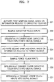
- FIGS. 6 and 7 are flowcharts of an operating method of a touchscreen controller, according to embodiments of the inventive concept.
- an operation related to capacitive touches and an operation related to force touches may be independently performed, and thus capacitive touch inputs for sensing capacitive touches and force touch inputs for sensing force touches may be asynchronously sampled.
- a plurality of capacitive touch inputs may be simultaneously sampled by the touchscreen controller (S 11 ), and the sampled capacitive touch inputs may be sequentially converted into digital signals by a single ADC (e.g., a common ADC) (S 12 ).
- a single ADC e.g., a common ADC
- a plurality of force touch inputs may be simultaneously sampled (S 13 ), and the sampled force touch inputs may be sequentially converted into digital signals by the common ADC (S 14 ).
- Touch information including information indicating whether a touch is made, a location of the touch, a force of the touch, etc. may be generated by processing the capacitive touch inputs and the force touch inputs converted into the digital signals (S 15 ).
- the touchscreen controller may assert a first sampling signal QS 1 based on information related to capacitive touches (S 21 ).
- a plurality of capacitive touch inputs may be sampled based on the asserted first sampling signal QS 1 (S 22 ).
- the sampled capacitive touch inputs may be sequentially converted into digital signals.
- some capacitive touch inputs may be sequentially converted into digital signals (S 23 ), and a second sampling signal QS 2 may be asserted based on information related to force touches while the capacitive touch inputs are being converted into digital signals (S 24 ).
- a plurality of force touch inputs may be sampled based on the asserted second sampling signal QS 2 (S 25 ). Since only the force touch inputs are selectively sampled, the other capacitive touch inputs which are sampled but not yet converted into digital signals may be retained as the sampled data.
- the other capacitive touch inputs may be sequentially converted into digital signals (S 26 ).
- the force touch inputs may be sequentially converted into digital signals (S 27 ).
- FIG. 8 is a circuit diagram showing an example of an S/H block 310 according to some embodiments of the inventive concept
- FIGS. 9 and 10 are waveform diagrams showing examples of operation of the S/H block 310 .
- a touchscreen controller 300 may include the S/H block 310 , an amplifier 320 , and an ADC 330 .
- the circuits illustrated in FIG. 8 the circuits described above in relation to the previous embodiments will not be described in detail herein.
- the S/H block 310 may include a plurality of S/H circuits corresponding to a plurality of channels. According to some embodiments, the S/H circuits of the S/H block 310 are not limited to a certain touch scheme but may receive touch inputs based on various touch schemes. For example, the S/H circuits of the S/H block 310 may receive capacitive touch inputs or force touch inputs as described above. According to some embodiments of the inventive concept, some S/H circuits of the S/H block 310 may receive capacitive touch inputs, and the other S/H circuits may receive force touch inputs.
- the S/H block 310 includes A+B S/H circuits and that the A S/H circuits (e.g., first S/H circuits) receive capacitive touch inputs whereas the other B S/H circuits (e.g., second S/H circuits) receive force touch inputs.
- a S/H circuits e.g., first S/H circuits
- B S/H circuits e.g., second S/H circuits
- the S/H circuits of the S/H block 310 may be controlled based on a common sampling signal QS.
- a common sampling signal QS For example, as the sampling signal QS is commonly provided to the A+B S/H circuits of the S/H block 310 , capacitive touch inputs V 1 _ 1 to V 1 _A and force touch inputs V 2 _ 1 to V 2 _B may be simultaneously sampled.
- first output control signals QH[1 ⁇ A] are sequentially asserted after the sampling signal QS is asserted, the capacitive touch inputs V 1 _ 1 to V 1 _A may be sequentially provided to the ADC 330 through the amplifier 320 .
- the force touch inputs V 2 _ 1 to V 2 _B may be sequentially provided to the ADC 330 through the amplifier 320 . That is, according to the embodiments of FIG. 9 , the sampling signal QS may not be separately asserted for the capacitive touch inputs V 1 _ 1 to V 1 _A and the force touch inputs V 2 _ 1 to V 2 _B but may be asserted one time to simultaneously sample the capacitive touch inputs V 1 _ 1 to V 1 _A and the force touch inputs V 2 _ 1 to V 2 _B.
- exclusive S/H circuits for the capacitive touch inputs V 1 _ 1 to V 1 _A and the force touch inputs V 2 _ 1 to V 2 _B may not be separately provided but the ADC 330 may be shared by the A+B S/H circuits.
- the sampling signal QS for sampling the capacitive touch inputs V 1 _ 1 to V 1 _A and the force touch inputs V 2 _ 1 to V 2 _B is asserted only one time in a single sampling cycle, and thus both of the capacitive touch inputs V 1 _ 1 to V 1 _A and the force touch inputs V 2 _ 1 to V 2 _B may be normally converted into digital signals.
- FIG. 10 shows another example of operation of the touchscreen controller 300 illustrated in FIG. 8 .
- the S/H block 310 may be controlled based on the common sampling signal QS, and the sampling signal QS may be asserted at least two times to sample the capacitive touch inputs V 1 _ 1 to V 1 _A and the force touch inputs V 2 _ 1 to V 2 _B.
- a process based on capacitive touches and a process based on force touches may be independently performed, and thus a first timing for asserting the sampling signal QS may be controlled based on the capacitive touch process whereas a second timing for asserting the sampling signal QS may be controlled based on the force touch process.
- the sampling signal QS may be asserted at a timing before the first output control signals QH[1 ⁇ A] are asserted, and thus the capacitive touch inputs V 1 _ 1 to V 1 _A may be stored in the first S/H circuits of the S/H block 310 . Thereafter, as the first output control signals QH[1 ⁇ A] are sequentially asserted, the capacitive touch inputs V 1 _ 1 to V 1 _A may be sequentially provided to the ADC 330 through the amplifier 320 .
- the sampling signal QS may be asserted again to sample the force touch inputs V 2 _ 1 to V 2 _B.
- the force touch inputs V 2 _ 1 to V 2 _B may be stored in the second S/H circuits of the S/H block 310 .
- the force touch inputs V 2 _ 1 to V 2 _B may be sequentially provided to the ADC 330 through the amplifier 320 .
- the sampling signal QS for sampling the force touch inputs V 2 _ 1 to V 2 _B may be asserted at a timing after all of the first output control signals QH[1 ⁇ A] are asserted and before the second output control signals QA[1 ⁇ B] are asserted.
- the sampling signal QS is asserted to sample the force touch inputs V 2 _ 1 to V 2 _B, since all of the sampled and stored capacitive touch inputs V 1 _ 1 to V 1 _A are converted into digital signals, information related to capacitive touches may be normally processed.
- the sampling signal QS may be asserted using information related to generation of an output control signal in addition to information related to processing of capacitive and force touches.
- the sampling signal QS may be asserted to sample the capacitive touch inputs V 1 _ 1 to V 1 _A, and then may be asserted again to sample the force touch inputs V 2 _ 1 to V 2 _B based on information indicating that all of the first output control signals QH[1 ⁇ A] are asserted.
- the second output control signals QA[1 ⁇ B] may be asserted based on information indicating that the sampling signal QS is asserted again, and thus activation of the second output control signals QA[1 ⁇ B] before the sampling signal QS for sampling the force touch inputs V 2 _ 1 to V 2 _B is asserted may be prevented.
- the S/H block 310 may process touch inputs based on various touch schemes, the number of S/H circuits included in the touchscreen controller 300 may be reduced.
- the touchscreen controller 300 may operate in various modes. For example, when force sensing is inasserted, all S/H circuits in the S/H block 310 may be used to sample capacitive touch inputs.
- FIG. 11 is a block diagram showing an example in which a touchscreen controller according to embodiments of the inventive concept is implemented as a touch-display driver IC (TDDI) 400 .
- the TDDI 400 may include a touchscreen controller (TSC) block 410 and a display driver IC (DDI) block 420 .
- TSC touchscreen controller
- DDI display driver IC
- the TDDI 400 may be implemented as a single semiconductor chip, and thus the TSC block 410 and the DDI block 420 may be integrated on the same semiconductor chip.
- the TSC block 410 may include various elements for processing touch inputs based on various touch schemes according to the afore-described embodiments.
- the TSC block 410 may include a first S/H block 411 , a second S/H block 412 , an ADC 413 , and a control signal generator 414 .
- the TSC block 410 may receive sensed signals based on two or more touch schemes, and perform an AFE operation on the received sensed signals to provide two or more types of touch inputs to the first and second S/H blocks 411 and 412 .
- a single ADC 413 may be provided to correspond to a plurality of S/H circuits included in the first and second S/H blocks 411 and 412 .
- the ADC 413 may sequentially receive a plurality of capacitive touch inputs and a plurality of force touch inputs and convert the same into digital signals according to the afore-described embodiments.
- the control signal generator 414 may generate various control signals for controlling the first and second S/H blocks 411 and 412 according to the afore-described embodiments, based on at least one type of information. For example, the control signal generator 414 may generate a first sampling signal QS 1 for sampling the capacitive touch inputs, a second sampling signal QS 2 for sampling the force touch inputs, a first output control signal QH for controlling a timing for outputting the sampled capacitive touch inputs to the ADC 413 , and a second output control signal QA for controlling a timing for outputting the sampled force touch inputs to the ADC 413 .
- the DDI block 420 may include a timing controller 421 and a source driver 422 as elements for displaying an image on a display panel (not shown). Although not shown in FIG. 11 , the DDI block 420 may further include various other elements for displaying the image, e.g., a gate driver and a power generator.
- the timing controller 421 may generate various types of timing information TI in relation to the display operation. For example, the timing controller 421 may generate a vertical synchronization signal or a horizontal synchronization signal in relation to the display operation, or generate various types of timing information for controlling generation of a common electrode voltage or a gate line signal.
- the TSC block 410 may use at least one type of the timing information TI received from the timing controller 421 . For instance, the TSC block 410 may perform the above-described sampling operation based on the timing information TI received from the timing controller 421 .
- the sensed signals may have noise due to driving of various types of electrodes provided on a display panel (e.g., common voltage electrodes), and the TSC block 410 may perform the sensing operation or the sampling operation according to the afore-described embodiments at a timing when the noise is minimized based on the timing information TI.
- the control signal generator 414 may generate the first and second sampling signals QS 1 and QS 2 based on various types of information according to the afore-described embodiments. For example, the control signal generator 414 may generate the first and second sampling signals QS 1 and QS 2 based on timings related to an AFE operation in the TSC block 410 . Otherwise, the control signal generator 414 may generate the first and second sampling signals QS 1 and QS 2 based on the timing information TI received from the timing controller 421 . In some embodiments, the control signal generator 414 may generate the first and second sampling signals QS 1 and QS 2 based on the timings related to the AFE operation together with the timing information TI received from the timing controller 421 .
- various signals other than the timing information TI may be transmitted and received between the TSC block 410 and the DDI block 420 .
- the DDI block 420 may provide signals for controlling various modes related to a touchscreen operation, to the TSC block 410 , provide various types of information indicating a state of the TDDI 400 (e.g., a sleep state and a power-down state), to the TSC block 410 , or generate various voltages used in the TSC block 410 and provide the same to the TSC block 410 .
- FIG. 12 is a block diagram showing an example in which a touchscreen controller 500 according to embodiments of the inventive concept is implemented as a chip separate from a DDI.
- the touchscreen controller 500 may include an AFE 510 , an ADC 520 , a timing manager 530 , and a control signal generator 540 .
- the AFE 510 may include various circuits for processing sensed signals received through a plurality of channels.
- the AFE 510 may include a capacitive touch circuit 511 for generating capacitive touch inputs and a force touch circuit 512 for generating force touch inputs.
- the AFE 510 may further include a first S/H block 513 and a second S/H block 514 .
- the ADC 520 is shared by the first and second S/H blocks 513 and 514 .
- FIG. 12 shows that the ADC 520 is provided outside the AFE 510 , the ADC 520 may be provided inside the AFE 510 .
- the timing manager 530 may control various timing operations related to a touchscreen operation.
- the timing manager 530 may provide timing information Info_ts to the control signal generator 540 .
- the control signal generator 540 may generate one or more control signals Ctrl_CT for controlling the capacitive touch circuit 511 in the AFE 510 and generate one or more control signals Ctrl FT for controlling the force touch circuit 512 , based on the timing information Info_ts.
- the control signal generator 540 may generate a first sampling signal QS 1 , a second sampling signal QS 2 , a first output control signal QH, and a second output control signal QA based on the timing information Info_ts.
- an activation timing of the first sampling signal QS 1 may be controlled based on the control signals Ctrl_CT.
- the activation timing of the first sampling signal QS 1 may be controlled in relation to an operation in the capacitive touch circuit 511 .
- the activation timing of the first sampling signal QS 1 may be controlled in relation to an integration operation in the capacitive touch circuit 511 .
- an activation timing of the second sampling signal QS 2 may be controlled based on the control signals Ctrl_FT.
- the first output control signal QH may be generated in synchronization with the first sampling signal QS 1
- the second output control signal QA may be generated in synchronization with the second sampling signal QS 2 .
- the control signal generator 540 may generate control signals having waveforms based on various schemes according to the afore-described embodiments.
- the touchscreen controller 500 may receive at least one type of timing information TI related to a display driving operation, from the external DDI, and the control signal generator 540 may generate the control signals having waveforms based on various schemes by further using the timing information TI.
- FIG. 13 is a block diagram of a touchscreen system 600 according to further embodiments of the inventive concept.
- the touchscreen system 600 may include a touchscreen panel 610 and a touchscreen controller 620 , and the touchscreen controller 620 may be connected to the touchscreen panel 610 through a plurality of channels.
- the channels may be divided into two or more groups.
- a first channel group G_CH 1 and a second channel group G_CH 2 are used to describe the embodiments of the inventive concept.
- Each channel group may include a plurality of channels connected to capacitive sensing electrodes and a plurality of channels connected to force sensing electrodes. As such, each channel group may deliver a plurality of sensed signals related to capacitive touches and a plurality of sensed signals related to force touches.
- the touchscreen controller 620 may include a plurality of S/H block groups (e.g., first and second S/H block groups).
- Each S/H block group may include first and second S/H blocks according to the afore-described embodiments.
- the first S/H block group may include first and second S/H blocks 611 and 612
- the second S/H block group may include first and second S/H blocks 613 and 614 .
- each S/H block group may sample capacitive touch inputs and force touch inputs.
- the first S/H block 611 may sample capacitive touch inputs V 1 _ 1 to V 1 _A, and the second S/H block 612 may sample force touch inputs V 2 _ 1 to V 2 _B.
- the touchscreen controller 620 may further include a plurality of ADCs (e.g., first and second ADCs 621 and 622 ), and each ADC may correspond to each S/H block group.
- each ADC may correspond to each S/H block group.
- the first ADC 621 may correspond to the first S/H block group
- the second ADC 622 may correspond to the second S/H block group.
- the touchscreen controller 620 may further include a DSP 630 for receiving digital-converted touch inputs from the first and second ADCs 621 and 622 .
- Each S/H block group may be controlled based on a first sampling signal, a second sampling signal, and first and second output control signals according to the afore-described embodiments.
- the first and second sampling signals and the first and second output control signals may have waveforms according to the afore-described embodiments, and each S/H block group may sample touch inputs based on different touch schemes and output the same according to the afore-described embodiments.
- FIG. 13 by varying placement of S/H block groups and ADCs based on the number of channels, the speed of a process for generating touch information may be increased.
- FIG. 14 is a circuit diagram showing an example of a touchscreen controller 700 according to some embodiments of the inventive concept.
- the touchscreen controller 700 may include a first S/H block 711 for sampling capacitive touch inputs V 1 _ 1 to V 1 _A, a second S/H block 712 for sampling force touch inputs V 2 _ 1 to V 2 _B, and an ADC 720 shared by the first and second S/H blocks 711 and 712 .
- the first S/H block 711 may include a plurality of first S/H circuits
- the second S/H block 712 may include a plurality of second S/H circuits.
- the first S/H block 711 may perform a sampling operation based on a first sampling signal QS 1
- the second S/H block 712 may perform a sampling operation based on a second sampling signal QS 2 generated independently of the first sampling signal QS 1
- the touchscreen controller 700 may further include an amplifier block 713 including a plurality of amplifiers corresponding to the first S/H circuits and the second S/H circuits.
- the capacitive touch inputs V 1 _ 1 to V 1 _A may be simultaneously amplified and the force touch inputs V 2 _ 1 to V 2 _B may be simultaneously amplified by the amplifiers, and the amplified capacitive touch inputs V 1 _ 1 to V 1 _A and the amplified force touch inputs V 2 _ 1 to V 2 _B may be sequentially provided to the ADC 720 through switches.
- the amplified touch inputs may be stably provided to the ADC 720 by the amplifiers.
- FIG. 15 is a block diagram showing an example of a touchscreen controller 800 according to some embodiments of the inventive concept.
- the touchscreen controller 800 may include a plurality of S/H blocks (e.g., first, second, and third S/H blocks 811 , 812 , and 813 ), an ADC 820 shared by the first, second, and third S/H blocks 811 , 812 , and 813 , and a DSP 830 for receiving digital-converted touch inputs.
- S/H blocks e.g., first, second, and third S/H blocks 811 , 812 , and 813
- ADC 820 shared by the first, second, and third S/H blocks 811 , 812 , and 813
- DSP 830 for receiving digital-converted touch inputs.
- the first S/H block 811 may sample capacitive touch inputs V 1 _ 1 to V 1 _A, and the second S/H block 812 may sample force touch inputs V 2 _ 1 to V 2 _B. As in the afore-described embodiments, the first S/H block 811 may perform the sampling operation in response to a first sampling signal QS 1 , and the second S/H block 812 may perform the sampling operation in response to a second sampling signal QS 2 .
- the touchscreen controller 800 may process various signals which are required to be converted into digital signals regardless of a touch sensing operation therein (e.g., another type of inputs V 3 _ 1 to V 3 _C). In this case, the touchscreen controller 800 may use the ADC 820 , which is commonly used for capacitive sensing and force sensing, to convert the other type of inputs V 3 _ 1 to V 3 _C into digital signals.
- the ADC 820 which is commonly used for capacitive sensing and force sensing
- the third S/H block 813 may sample the other type of inputs V 3 _ 1 to V 3 _C in response to a third sampling signal QS 3 . Since the third sampling signal QS 3 selectively controls the third S/H block 813 , the third sampling signal QS 3 may be generated regardless of the first and second sampling signals QS 1 and QS 2 . That is, the third sampling signal QS 3 may be asserted while the first and second S/H blocks 811 and 812 are being output.
- the other type of inputs V 3 _ 1 to V 3 _C may be output to the ADC 820 after the capacitive touch inputs V 1 _ 1 to V 1 _A and the force touch inputs V 2 _ 1 to V 2 _B are provided to the ADC 820 .
- the other type of inputs V 3 _ 1 to V 3 _C may include various types of signals.
- the touchscreen controller 800 may detect levels of various internal voltages and, in this case, the various internal voltages to be detected may correspond to the other type of inputs V 3 _ 1 to V 3 _C.
- the touchscreen controller 800 may detect levels of various voltages applied to external elements and, in this case, the various external voltages to be detected may correspond to the other type of inputs V 3 _ 1 to V 3 _C.
- levels of voltages applied to a plurality of channels connected to the touchscreen controller 800 may be detected and, in this case, the voltages applied to the channels may correspond to the other type of inputs V 3 _ 1 to V 3 _C.
- a touchscreen controller a touchscreen system including the same, and an operating method of the touchscreen controller, according to the inventive concept, the number of ADCs for processing touch inputs based on various touch schemes, and thus the size of a semiconductor chip for implementing the touchscreen controller may be reduced and power consumption may also be reduced.
Landscapes
- Engineering & Computer Science (AREA)
- General Engineering & Computer Science (AREA)
- Theoretical Computer Science (AREA)
- Human Computer Interaction (AREA)
- Physics & Mathematics (AREA)
- General Physics & Mathematics (AREA)
- Position Input By Displaying (AREA)
Abstract
Description
Claims (20)
Applications Claiming Priority (2)
| Application Number | Priority Date | Filing Date | Title |
|---|---|---|---|
| KR10-2017-0123657 | 2017-09-25 | ||
| KR1020170123657A KR102349419B1 (en) | 2017-09-25 | 2017-09-25 | Touch screen controller, Touch screen system and Operating method of touch screen controller |
Publications (2)
| Publication Number | Publication Date |
|---|---|
| US20190095031A1 US20190095031A1 (en) | 2019-03-28 |
| US10642410B2 true US10642410B2 (en) | 2020-05-05 |
Family
ID=65808416
Family Applications (1)
| Application Number | Title | Priority Date | Filing Date |
|---|---|---|---|
| US15/927,352 Active 2038-08-04 US10642410B2 (en) | 2017-09-25 | 2018-03-21 | Touchscreen controller, touchscreen system including the same, and operating method of the touchscreen controller |
Country Status (3)
| Country | Link |
|---|---|
| US (1) | US10642410B2 (en) |
| KR (1) | KR102349419B1 (en) |
| CN (1) | CN109558027B (en) |
Families Citing this family (3)
| Publication number | Priority date | Publication date | Assignee | Title |
|---|---|---|---|---|
| CN108459772B (en) * | 2018-03-26 | 2021-05-11 | 京东方科技集团股份有限公司 | Touch module, driving method thereof and display device |
| US11703983B2 (en) * | 2020-03-25 | 2023-07-18 | Sensortek Technology Corp | Capacitance sensing circuit |
| KR102919920B1 (en) * | 2021-12-09 | 2026-01-29 | 엘지디스플레이 주식회사 | Touch driving circuit and touch display device |
Citations (12)
| Publication number | Priority date | Publication date | Assignee | Title |
|---|---|---|---|---|
| US8274481B2 (en) | 2004-10-22 | 2012-09-25 | Sharp Kabushiki Kaisha | Display device with touch sensor, and drive method for the device |
| US20130215053A1 (en) | 2012-02-17 | 2013-08-22 | Elan Microelectronics Corporation | Anti-interference driving method of touch panel and touch panel device using the same |
| US8519974B2 (en) | 2010-01-19 | 2013-08-27 | Sony Corporation | Touch sensing device, touch screen device comprising the touch sensing device, mobile device, method for sensing a touch and method for manufacturing a touch sensing device |
| KR101378345B1 (en) | 2012-08-13 | 2014-03-27 | 엘지디스플레이 주식회사 | Display Device Including Touch Module And Method Of Driving The Same |
| US8780074B2 (en) | 2011-07-06 | 2014-07-15 | Sharp Kabushiki Kaisha | Dual-function transducer for a touch panel |
| US8890841B2 (en) | 2013-03-13 | 2014-11-18 | 3M Innovative Properties Company | Capacitive-based touch apparatus and method therefor, with reduced interference |
| US8947277B2 (en) | 2012-02-27 | 2015-02-03 | Samsung Electronics Co., Ltd. | Multi-channel sample-and-hold circuit and analog-to-digital converter using the same |
| US20150097583A1 (en) | 2013-10-04 | 2015-04-09 | Microchip Technology Incorporated | Multiple channel capacitive voltage divider scanning method and apparatus |
| US9086439B2 (en) | 2011-02-25 | 2015-07-21 | Maxim Integrated Products, Inc. | Circuits, devices and methods having pipelined capacitance sensing |
| US20160041217A1 (en) | 2014-08-11 | 2016-02-11 | Lsis Co., Ltd. | On-line status diagnosis device and on-line status diagnosis method for electric power utilities |
| US9329739B2 (en) | 2012-11-13 | 2016-05-03 | Lg Display Co., Ltd. | Touch sensing system and method of controlling power consumption thereof, and display device using the same |
| US20160124544A1 (en) | 2014-11-05 | 2016-05-05 | Samsung Electronics Co., Ltd. | Touch analog front end and touch sensor controller having the same |
Family Cites Families (8)
| Publication number | Priority date | Publication date | Assignee | Title |
|---|---|---|---|---|
| TWI363290B (en) * | 2008-10-29 | 2012-05-01 | Myson Century Inc | Signal conversion control circuit for touch screen and method thereof |
| DE102009046177A1 (en) * | 2008-10-30 | 2010-06-10 | Samsung Electronics Co., Ltd., Suwon | Touch data generator |
| CN102073425A (en) * | 2010-12-29 | 2011-05-25 | 广东中显科技有限公司 | Touch control system of touch screen |
| US8576197B2 (en) * | 2011-05-16 | 2013-11-05 | Pixart Imaging, Inc. | Noise blanking for capacitive touch displays |
| CN102830882B (en) * | 2012-09-04 | 2015-05-13 | 北京集创北方科技有限公司 | Touch detection circuit of capacitive touch screen |
| KR102125404B1 (en) * | 2013-10-15 | 2020-06-22 | 엘지디스플레이 주식회사 | Touch sensing system and diplay device |
| KR102243635B1 (en) * | 2014-11-21 | 2021-04-26 | 엘지디스플레이 주식회사 | Touch sensing circuit, display device using the touch sensor circuit, and touch sensing method |
| US9886136B2 (en) * | 2015-06-22 | 2018-02-06 | Samsung Electronics Co., Ltd. | Touch screen controller using adaptive filter control and touch screen system having the same |
-
2017
- 2017-09-25 KR KR1020170123657A patent/KR102349419B1/en active Active
-
2018
- 2018-03-21 US US15/927,352 patent/US10642410B2/en active Active
- 2018-07-23 CN CN201810811610.8A patent/CN109558027B/en active Active
Patent Citations (12)
| Publication number | Priority date | Publication date | Assignee | Title |
|---|---|---|---|---|
| US8274481B2 (en) | 2004-10-22 | 2012-09-25 | Sharp Kabushiki Kaisha | Display device with touch sensor, and drive method for the device |
| US8519974B2 (en) | 2010-01-19 | 2013-08-27 | Sony Corporation | Touch sensing device, touch screen device comprising the touch sensing device, mobile device, method for sensing a touch and method for manufacturing a touch sensing device |
| US9086439B2 (en) | 2011-02-25 | 2015-07-21 | Maxim Integrated Products, Inc. | Circuits, devices and methods having pipelined capacitance sensing |
| US8780074B2 (en) | 2011-07-06 | 2014-07-15 | Sharp Kabushiki Kaisha | Dual-function transducer for a touch panel |
| US20130215053A1 (en) | 2012-02-17 | 2013-08-22 | Elan Microelectronics Corporation | Anti-interference driving method of touch panel and touch panel device using the same |
| US8947277B2 (en) | 2012-02-27 | 2015-02-03 | Samsung Electronics Co., Ltd. | Multi-channel sample-and-hold circuit and analog-to-digital converter using the same |
| KR101378345B1 (en) | 2012-08-13 | 2014-03-27 | 엘지디스플레이 주식회사 | Display Device Including Touch Module And Method Of Driving The Same |
| US9329739B2 (en) | 2012-11-13 | 2016-05-03 | Lg Display Co., Ltd. | Touch sensing system and method of controlling power consumption thereof, and display device using the same |
| US8890841B2 (en) | 2013-03-13 | 2014-11-18 | 3M Innovative Properties Company | Capacitive-based touch apparatus and method therefor, with reduced interference |
| US20150097583A1 (en) | 2013-10-04 | 2015-04-09 | Microchip Technology Incorporated | Multiple channel capacitive voltage divider scanning method and apparatus |
| US20160041217A1 (en) | 2014-08-11 | 2016-02-11 | Lsis Co., Ltd. | On-line status diagnosis device and on-line status diagnosis method for electric power utilities |
| US20160124544A1 (en) | 2014-11-05 | 2016-05-05 | Samsung Electronics Co., Ltd. | Touch analog front end and touch sensor controller having the same |
Also Published As
| Publication number | Publication date |
|---|---|
| US20190095031A1 (en) | 2019-03-28 |
| CN109558027B (en) | 2024-04-19 |
| KR102349419B1 (en) | 2022-01-10 |
| KR20190034984A (en) | 2019-04-03 |
| CN109558027A (en) | 2019-04-02 |
Similar Documents
| Publication | Publication Date | Title |
|---|---|---|
| CN106409218B (en) | It is integrated with the display device and its driving method of touch sensor | |
| KR102364097B1 (en) | Touch sensor integrated type display device and touch sensing method of the same | |
| US9367168B2 (en) | Touch screen system and method of driving the same | |
| KR102326169B1 (en) | Touch sensor integrated type display device and touch sensing method of the same | |
| KR102102881B1 (en) | Touch sensing system and method of controlling power consumption | |
| US9846502B2 (en) | Touch sensor and display apparatus including the same | |
| KR102243635B1 (en) | Touch sensing circuit, display device using the touch sensor circuit, and touch sensing method | |
| KR102347129B1 (en) | Touch screen device and method for driving the same | |
| CN104951157B (en) | Capacitive touch device and method for detecting active pen and object | |
| US11556209B2 (en) | Touch sensing device for compensating for phase error of active pen and method thereof | |
| WO2009142345A1 (en) | Touch sensor device and the method of switching operation mode thereof | |
| JP2008198211A (en) | Display device and driving method thereof | |
| US10540041B2 (en) | Touch processor, touch display driver integrated circuit chip including touch processor, and method of operating touch processor | |
| US10642410B2 (en) | Touchscreen controller, touchscreen system including the same, and operating method of the touchscreen controller | |
| KR102410103B1 (en) | Display Device Having the Touch Sensor | |
| US9952721B2 (en) | Touch panel, information recording medium, and information acquisition method | |
| KR101503106B1 (en) | Apparatus and method for driving touch screen | |
| US10108302B2 (en) | Touch driving system with low display noise | |
| TWI756987B (en) | Image sensing system and circuit | |
| CN112863440A (en) | Pixel compensation circuit, driving method thereof and display device | |
| US11500495B2 (en) | Touch display device | |
| US20130278509A1 (en) | Input system utilizing stylus pen which receives electrical signals via connection link | |
| KR102182979B1 (en) | Sensing system | |
| KR20190020953A (en) | Touch screen | |
| KR102256037B1 (en) | Touch sensing system and display using the same |
Legal Events
| Date | Code | Title | Description |
|---|---|---|---|
| AS | Assignment |
Owner name: SAMSUNG ELECTRONICS CO., LTD., KOREA, REPUBLIC OF Free format text: ASSIGNMENT OF ASSIGNORS INTEREST;ASSIGNORS:LEE, KYUNG-HOON;CHOI, MICHAEL;REEL/FRAME:045301/0540 Effective date: 20180226 |
|
| FEPP | Fee payment procedure |
Free format text: ENTITY STATUS SET TO UNDISCOUNTED (ORIGINAL EVENT CODE: BIG.); ENTITY STATUS OF PATENT OWNER: LARGE ENTITY |
|
| STPP | Information on status: patent application and granting procedure in general |
Free format text: DOCKETED NEW CASE - READY FOR EXAMINATION |
|
| STPP | Information on status: patent application and granting procedure in general |
Free format text: NON FINAL ACTION MAILED |
|
| STPP | Information on status: patent application and granting procedure in general |
Free format text: RESPONSE TO NON-FINAL OFFICE ACTION ENTERED AND FORWARDED TO EXAMINER |
|
| STPP | Information on status: patent application and granting procedure in general |
Free format text: NOTICE OF ALLOWANCE MAILED -- APPLICATION RECEIVED IN OFFICE OF PUBLICATIONS |
|
| STCF | Information on status: patent grant |
Free format text: PATENTED CASE |
|
| MAFP | Maintenance fee payment |
Free format text: PAYMENT OF MAINTENANCE FEE, 4TH YEAR, LARGE ENTITY (ORIGINAL EVENT CODE: M1551); ENTITY STATUS OF PATENT OWNER: LARGE ENTITY Year of fee payment: 4 |