US10637485B2 - Oscillator arrangement for time-to-digital converter for large array of time-of-flight image sensor devices - Google Patents
Oscillator arrangement for time-to-digital converter for large array of time-of-flight image sensor devices Download PDFInfo
- Publication number
- US10637485B2 US10637485B2 US15/941,411 US201815941411A US10637485B2 US 10637485 B2 US10637485 B2 US 10637485B2 US 201815941411 A US201815941411 A US 201815941411A US 10637485 B2 US10637485 B2 US 10637485B2
- Authority
- US
- United States
- Prior art keywords
- oscillators
- oscillator
- time
- arrangement according
- oscillator arrangement
- Prior art date
- Legal status (The legal status is an assumption and is not a legal conclusion. Google has not performed a legal analysis and makes no representation as to the accuracy of the status listed.)
- Active, expires
Links
- 230000008878 coupling Effects 0.000 claims abstract description 44
- 238000010168 coupling process Methods 0.000 claims abstract description 44
- 238000005859 coupling reaction Methods 0.000 claims abstract description 44
- 230000001360 synchronised effect Effects 0.000 claims abstract description 5
- 230000010355 oscillation Effects 0.000 claims abstract description 4
- 239000003990 capacitor Substances 0.000 claims description 9
- 238000001514 detection method Methods 0.000 description 11
- 238000003384 imaging method Methods 0.000 description 6
- 238000005259 measurement Methods 0.000 description 3
- 238000013139 quantization Methods 0.000 description 3
- 238000010791 quenching Methods 0.000 description 3
- 230000000171 quenching effect Effects 0.000 description 3
- 230000001052 transient effect Effects 0.000 description 3
- XUIMIQQOPSSXEZ-UHFFFAOYSA-N Silicon Chemical compound [Si] XUIMIQQOPSSXEZ-UHFFFAOYSA-N 0.000 description 2
- 238000000034 method Methods 0.000 description 2
- 230000003287 optical effect Effects 0.000 description 2
- 238000005070 sampling Methods 0.000 description 2
- 229910052710 silicon Inorganic materials 0.000 description 2
- 239000010703 silicon Substances 0.000 description 2
- 230000035508 accumulation Effects 0.000 description 1
- 238000009825 accumulation Methods 0.000 description 1
- 230000001427 coherent effect Effects 0.000 description 1
- 230000002596 correlated effect Effects 0.000 description 1
- 230000000875 corresponding effect Effects 0.000 description 1
- 230000007423 decrease Effects 0.000 description 1
- 230000001934 delay Effects 0.000 description 1
- 238000010586 diagram Methods 0.000 description 1
- 238000005516 engineering process Methods 0.000 description 1
- 238000001914 filtration Methods 0.000 description 1
- 238000002347 injection Methods 0.000 description 1
- 239000007924 injection Substances 0.000 description 1
- 230000007774 longterm Effects 0.000 description 1
- 230000001902 propagating effect Effects 0.000 description 1
- 230000003068 static effect Effects 0.000 description 1
Images


Classifications
-
- H—ELECTRICITY
- H03—ELECTRONIC CIRCUITRY
- H03L—AUTOMATIC CONTROL, STARTING, SYNCHRONISATION OR STABILISATION OF GENERATORS OF ELECTRONIC OSCILLATIONS OR PULSES
- H03L7/00—Automatic control of frequency or phase; Synchronisation
- H03L7/06—Automatic control of frequency or phase; Synchronisation using a reference signal applied to a frequency- or phase-locked loop
- H03L7/08—Details of the phase-locked loop
- H03L7/099—Details of the phase-locked loop concerning mainly the controlled oscillator of the loop
- H03L7/0995—Details of the phase-locked loop concerning mainly the controlled oscillator of the loop the oscillator comprising a ring oscillator
-
- G—PHYSICS
- G04—HOROLOGY
- G04F—TIME-INTERVAL MEASURING
- G04F10/00—Apparatus for measuring unknown time intervals by electric means
- G04F10/005—Time-to-digital converters [TDC]
-
- G—PHYSICS
- G01—MEASURING; TESTING
- G01S—RADIO DIRECTION-FINDING; RADIO NAVIGATION; DETERMINING DISTANCE OR VELOCITY BY USE OF RADIO WAVES; LOCATING OR PRESENCE-DETECTING BY USE OF THE REFLECTION OR RERADIATION OF RADIO WAVES; ANALOGOUS ARRANGEMENTS USING OTHER WAVES
- G01S17/00—Systems using the reflection or reradiation of electromagnetic waves other than radio waves, e.g. lidar systems
- G01S17/88—Lidar systems specially adapted for specific applications
- G01S17/89—Lidar systems specially adapted for specific applications for mapping or imaging
-
- G—PHYSICS
- G01—MEASURING; TESTING
- G01S—RADIO DIRECTION-FINDING; RADIO NAVIGATION; DETERMINING DISTANCE OR VELOCITY BY USE OF RADIO WAVES; LOCATING OR PRESENCE-DETECTING BY USE OF THE REFLECTION OR RERADIATION OF RADIO WAVES; ANALOGOUS ARRANGEMENTS USING OTHER WAVES
- G01S7/00—Details of systems according to groups G01S13/00, G01S15/00, G01S17/00
- G01S7/48—Details of systems according to groups G01S13/00, G01S15/00, G01S17/00 of systems according to group G01S17/00
- G01S7/483—Details of pulse systems
- G01S7/486—Receivers
- G01S7/4865—Time delay measurement, e.g. time-of-flight measurement, time of arrival measurement or determining the exact position of a peak
-
- H—ELECTRICITY
- H03—ELECTRONIC CIRCUITRY
- H03H—IMPEDANCE NETWORKS, e.g. RESONANT CIRCUITS; RESONATORS
- H03H7/00—Multiple-port networks comprising only passive electrical elements as network components
- H03H7/38—Impedance-matching networks
Definitions
- the present invention relates to integrated time-of-flight image sensor devices for 3D imaging applications.
- Time-resolved optical sensors have become important for various applications, such as PET, FLEM and LiDAR.
- These image sensor devices when implemented in CMOS, generally comprise avalanche photodiodes operating in Geiger mode, known as single photon avalanche diodes (SPAD), and time-to-digital converters which determine the time of arrival of photons.
- the photodiodes are arranged in an array of a sensor pixel area.
- One or more photodiodes are each coupled with one time-to-digital converter, so that in time-correlated operation mode, the timing of incoming photons which are periodically generated by a laser can be precisely measured so that an accurate 3D image reconstruction of the scanned scene can be obtained.
- Time-of-flight image sensors require high levels of accuracy and precision on time quantization typically using time-to-digital converters. Therefore, the availability of precise and uniform timing information over the sensor pixel area is required due to non-linearity and jitter.
- a single time-to-digital converter is used together with a distribution network as e.g. shown in Carimatto, A., et al., “A 67,392-SPAD PVTB-Compensated Multi-Channel Digital SiPM with 432 Column-Parallel 48 ps 17 b TDCs for Endoscopic Time-of-Flight PET”, ISSCC 2015.
- a single time-to-digital converter requires to be used together with a distribution network, high power consumption and non-linearity are imposed as multiple phases of an oscillator or the time-to-digital converter need to be routed over the sensor area.
- a further approach provides one time-to-digital converter per pixel which can lead to a lower power consumption, in case of a photon-starved application.
- those time-to-digital converters are required to operate in open loop and independently from each other, which is highly susceptible to process-voltage-temperature variations, jitter accumulations and non-linearity, as e.g. shown in Richardson, J., et al., “A 32 ⁇ 32 50 ps resolution 10-bit time to digital converter array in 130 nm CMOS for time correlated imaging”, CICC 2009.
- ring oscillators such as known from P. Kinget, “Integrated GHz voltage-controlled oscillators”, Springer, 1999.
- an oscillator arrangement for time-to-digital converters for a 3D image sensor device comprising:
- the above oscillator arrangement provides an oscillator grid which is at least partly spread over the sensor pixel area to provide timing information to time-to-digital converters each used by a portion of the pixels of the sensor pixel area.
- the time-to-digital converters are each associated to one of the oscillators of the oscillator arrangement which are mutually coupled with at least one oscillator of a neighbored time-to-digital converter.
- oscillator arrangement allows a mutual coupling at a fundamental frequency of the oscillators synchronizing the oscillators in phase and frequency and perform noise filtering of internal, uncorrelated noises sources. Further, the oscillators which have slightly different fundamental frequencies due to silicon imperfections and manufacturability variations and which have after start-up random phases, phase and frequency alignment will be reached very shortly after start-up. Furthermore, if due to a time-of-arrival sampling of one of the time-to-digital converters, a disturbance is induced into one of the oscillators, the oscillators of neighbored time-to-digital converters force the out-of-phase oscillator to realign without propagating the error indefinitely like in an open-loop scenario.
- oscillator arrangement for time-to-digital converters achieve a robust synchronization of timing signals supplied by the ring oscillators while further greatly reducing the phase noise which is at about the same frequency uncorrelated in different oscillators. Furthermore, it provides a low process-voltage-temperature dependency and similar power consumption of the sum of the number of oscillators, without extra power being spent in the synchronization.
- the coupling between two ring oscillators can be made by means of a coupling unit defining a coupling strength, wherein the coupling unit includes one or more coupling elements and particularly comprises one or more coupling resistances and/or one or more coupling capacitors and/or one or more inductances which have to be carefully selected as they influence largely the transient time.
- each of the at least one coupling unit may be respectively arranged between two neighboring oscillators of the array.
- each two neighboring ring oscillators of the array may be coupled with one of the at least one coupling unit.
- the plurality of oscillators may comprise a plurality of relaxation oscillators, LC-tank oscillators or micromechanical oscillators.
- the oscillators are formed as ring oscillators each comprising a number of inverters coupled with output to input interconnects in a closed loop, wherein each of the at least one coupling unit connects one output to input interconnect of one ring oscillator to another output to input interconnect of another ring oscillator.
- one output to input interconnect of the ring oscillator may be coupled to a counter wherein the output to input interconnect of one ring oscillator and the output to input interconnects of another one of the ring oscillators which are coupled via the coupling unit, have the same distance of the output to input interconnects coupled to the counter in terms of inverters.
- a PLL circuit may be provided which controls the oscillators depending on a reference frequency signal to adjust the frequency to a provided reference frequency.
- the PLL circuit may be an analog PLL circuit and configured to provide a common control voltage depending on one of the oscillators phases with respect to the reference frequency to control all oscillators.
- the PLL circuit may be a digital PLL (or digital word, in case of a digital PLL), shared among the oscillator, By implementing a single global PLL circuit slow temperature drifts can be tracked and compensated and a stable well-defined frequency can be provided, thereby reducing calibration requirements.
- a 3D image sensor device comprising:
- FIG. 1 schematically shows the configuration of a 3D imaging device in a cross-sectional view, based on stacking technology
- FIG. 2 shows a general configuration of an example of a photon detecting 3D imaging sensor device
- FIG. 3 shows a schematic view on a detection layer implementing time-to-digital converters, each having its own ring oscillator;
- FIG. 4 shows a diagram indicating the reduction of phase noise in an array of time-to-digital converters of different sizes
- FIGS. 5 a and 5 b show schematic examples of a circuitry of a coupling unit
- FIG. 6 shows a schematic view of two coupled ring oscillators
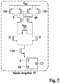
- FIG. 7 shows a schematic of a sense amplifier flip-flop for sampling phases of the ring oscillator.
- FIG. 1 Such an exemplary 3D image sensor device 1 is shown in FIG. 1 in a cross-sectional view.
- the 3D image sensor device 1 has a stacked configuration with a sensing layer 2 including the pixel sensors in an array 21 formed with one avalanche photodiodes operating in Geiger mode, also known as single photon avalanche diodes SPAD, per pixel.
- a sensing layer 2 including the pixel sensors in an array 21 formed with one avalanche photodiodes operating in Geiger mode, also known as single photon avalanche diodes SPAD, per pixel.
- SPAD single photon avalanche diodes
- a read-out circuitry 31 is coupled with the photodiode array 21 .
- the read-out circuitry 31 is implemented including time-to-digital converters, each associated to one or more of the pixels included in the sensing layer 2 .
- the time-to-digital converters each are associated to the pixels (photodiodes) of a portion of the pixel area, substantially a rectangular area portion.
- the time-to-digital converters are directly arranged under the respective pixel area of the sensing layer 2 in a stacked arrangement of the image sensor device 1 .
- DTOF direct time-of-flight
- SPAD single-photon avalanche diode
- FIG. 2 depicts the basic concept of a DTOF imaging sensor device according to the present invention.
- a diode laser 11 is controlled by a synchronization signal S sync provided by a pulse generator 12 so that a pulsed laser signal LS is directed onto an object O through one or more optical elements 13 , such as a beam collimator or the like.
- the pulsed laser signal is reflected by the object O onto a receiver side R.
- the receiver side R is formed by a photodiode array 14 onto which the reflected pulsed laser light LR is collected by a receiver optics 15 and detected by one or more of the photodiodes.
- the photodiodes may be formed by single-photon detecting diodes, such as SPADs.
- the signals from the photodiodes are received by means of a single quenching detector of a quenching detector array 16 .
- pulses of a respective detection signal Q 1 . . . n can be obtained based on the arrival time of a laser pulse of the reflected pulsed laser signal LR which has been received in the associated photodiode. So, depending on the number of photodiodes in the photodiode array 14 the number of detection signals Q 1 . . . n is obtained.
- the travel time of the pulsed laser signal to the object O and back to the photodiode array 14 depends on the distance of the object O. Therefore, the travel time of the pulsed laser signal corresponds to the distance of the portion of the object to be measured wherein the laser signal pulse has been detected and so provides a distance information to the pixel which is associated to the respective portion of the object.
- the travel time can be determined by a time-to-digital converter measuring a time difference between a pulse of the synchronization signal S sync and a corresponding pulse of the detection signals Q 1 . . . n .
- Each of the differences is indicative for a scanned pixel received by the photodiode array 14 .
- a common approach to cope with these detection signal pulses is to apply a first-come-win-all strategy in a pulse selection unit, so that only the quickest detection signal pulse is considered. After one detection, the pulse selection unit is reset or self-resets, being available for a new detection.
- FIG. 3 shows an array arrangement 5 of the time-to-digital converters 51 spread along the sensor area array 21 .
- Each time-to-digital converter 51 comprises an oscillator 52 and a measurement circuitry 53 which allows to measure a counter difference of a counter preferably continuously operated by the oscillator 52 .
- the counter difference serves as a time difference measure.
- the evenly distributed time-to-digital converters 51 result in evenly distributed oscillators 52 in an oscillator array
- the oscillators 52 of the neighboring time-to-digital converters 51 are each mutually coupled with one or more oscillators 52 of neighboring time-to-digital converters 51 of the array arrangement 5 .
- the coupling may be made between the oscillators 52 arranged closest to each other.
- the oscillators 52 can be formed as ring oscillators, relaxation oscillators, LC-tank oscillators or micromechanical oscillators. In the following it will be referred to ring oscillators for ease of description.
- the coupling is performed by means of a coupling unit 54 which is formed as an impedance.
- a coupling unit 54 which is formed as an impedance. This allows a mutual coupling at the fundamental frequency of the ring oscillators 51 , synchronizing them in phase and frequency or to keep them synchronized in phase and frequency. So, the time-to-digital converters can be operated in a synchronized manner. Further oscillators which have a different fundamental frequency and random phases are urged to align each other in phase and frequency shortly after start-up or after the phase of one of the ring oscillators 52 is disturbed.
- the selection of the coupling elements of the coupling unit 54 substantially influences the transient time.
- the coupling units 54 can be formed with one or more resistors and/or with one or more capacitors and/or with one or more inductors whose values are carefully selected to reduce transient time until phase locking (locking time).
- the chosen resistances and/or capacitances and/or inductances are selected depending on the strength of the oscillator themselves. If a system does not require super-fast locking time, weaker (higher resistances/lower capacitances) (more relaxed) coupling elements are desirable, thus reducing the stress in the neighbor oscillators upon a disturbance.
- phase noise is uncorrelated between the ring oscillators 52 so that the coupling contributes to a reduction of the phase noise according to 10 ⁇ log 10 (M), where M is the number of coupled oscillators.
- M is the number of coupled oscillators.
- FIGS. 5 a and 5 b show exemplary embodiments of the coupling unit 54 .
- the coupling unit of FIG. 5 a shows a series connection of a first capacitor, a first resistor and a second capacitor while the nodes between the first capacitor and the first resistor and between the first resistor and the second capacitor are each connected to a reference (ground) potential by means of grounding capacitors.
- the coupling unit 54 of FIG. 5 b differs from the embodiment of FIG. 5 a in that the first and second capacitors are replaced by resistances.
- Such a coupling unit can also be applied to LC-tank oscillators.
- FIG. 6 shows two coupled ring oscillators 52 .
- Each ring oscillator 52 has a number of inverters 55 which are coupled by output to input interconnects preferably in a differential manner.
- the ring oscillator 52 may comprise non-differential inverters or inverters coupled in a pseudo-differential manner.
- one output to input interconnect of an inverter 55 may be fed to a counter 56 which is incremented based on the fundamental frequency of the ring oscillator 52 .
- the coupling between two ring oscillators 52 is made by means of connecting the coupling unit 54 between one output of an inverter of one ring oscillator to an input of one of the inverters of another ring oscillator of a neighboring time to the digital converter.
- the coupling to a ring oscillator 52 of a neighboring tine-to-digital converter is not made at the output of the inverter which is also coupled to the counter 56 .
- the ring oscillators 52 should have similar or identical structure and the coupling should be made to the input of the same inverters 55 in the structure, i.e. the coupling should be made between the output to input interconnects between the inverters 55 having the same distance from the counter 56 in terms of number of inverters 55 .
- All output to input interconnects of the inverters 55 are coupled via sense amplifier flip-flops 60 to obtain a phase information further adding precision to the time measurement.
- FIG. 7 an example of a sense amplifier flip-flop 60 is shown which allows to latch a status of the ring oscillator 52 by means of the logic levels of a respective output to input interconnect (signals in and ⁇ circumflex over ( ) ⁇ in) depending on a signal TOF applied when a detection event occurs.
- the ring oscillators 52 may have a control input CTRL to be controlled by means of a negative feedback loop PLL circuit 58 to adjust the frequency to a precise and desirable frequency.
- the loop bandwidth is set to be low, so long latencies in the process don't create instability issues.
- the type of PLL may be an analog or digital PLL, even an external PLL can be used, since the loop bandwidth is low.
- the ring oscillators 52 are controlled by taking one of the oscillators phases and by providing a common voltage to control all oscillators.
- the PLL circuit 58 is configured to control the ring oscillators 52 by means of a control signal adapting their switching time based on a phase difference between a supplied reference frequency and an oscillation frequency of the oscillator arrangement.
- the mutually coupled oscillators will have the same frequency and locked phase by the end of the mutually injection process. However, the specific frequency and phase values are related to the overall performance of the array.
Landscapes
- Engineering & Computer Science (AREA)
- Physics & Mathematics (AREA)
- General Physics & Mathematics (AREA)
- Computer Networks & Wireless Communication (AREA)
- Radar, Positioning & Navigation (AREA)
- Remote Sensing (AREA)
- Electromagnetism (AREA)
- Transforming Light Signals Into Electric Signals (AREA)
Abstract
Description
-
- a plurality of oscillators arranged as an array each oscillator being associated to one time-to-digital converter;
- at least one coupling unit respectively arranged between at least two of the oscillators, so that oscillation in the at least two oscillators at a fundamental frequency is synchronized between the at least two coupled oscillators.
-
- a photodiode array providing a plurality of pixels;
- the above oscillator arrangement,
- time-to-digital converters each associated to one of the ring oscillators of the oscillator arrangement so that the respective ring oscillator provides a timing information to the respective time to digital converter.
Claims (10)
Priority Applications (1)
| Application Number | Priority Date | Filing Date | Title |
|---|---|---|---|
| US15/941,411 US10637485B2 (en) | 2018-03-30 | 2018-03-30 | Oscillator arrangement for time-to-digital converter for large array of time-of-flight image sensor devices |
Applications Claiming Priority (1)
| Application Number | Priority Date | Filing Date | Title |
|---|---|---|---|
| US15/941,411 US10637485B2 (en) | 2018-03-30 | 2018-03-30 | Oscillator arrangement for time-to-digital converter for large array of time-of-flight image sensor devices |
Publications (2)
| Publication Number | Publication Date |
|---|---|
| US20190305784A1 US20190305784A1 (en) | 2019-10-03 |
| US10637485B2 true US10637485B2 (en) | 2020-04-28 |
Family
ID=68055640
Family Applications (1)
| Application Number | Title | Priority Date | Filing Date |
|---|---|---|---|
| US15/941,411 Active 2038-10-27 US10637485B2 (en) | 2018-03-30 | 2018-03-30 | Oscillator arrangement for time-to-digital converter for large array of time-of-flight image sensor devices |
Country Status (1)
| Country | Link |
|---|---|
| US (1) | US10637485B2 (en) |
Cited By (1)
| Publication number | Priority date | Publication date | Assignee | Title |
|---|---|---|---|---|
| US10877133B2 (en) * | 2017-06-21 | 2020-12-29 | Sick Ag | Optoelectronic sensor and method of measuring the distance from an object |
Families Citing this family (2)
| Publication number | Priority date | Publication date | Assignee | Title |
|---|---|---|---|---|
| KR102317072B1 (en) * | 2019-12-17 | 2021-10-25 | 현대모비스 주식회사 | Method and apparatus for time-to-digital conversion in LiDAR system |
| CN114137558B (en) * | 2022-02-07 | 2022-04-29 | 杭州宏景智驾科技有限公司 | A control method, device and laser radar system for improving the precision of laser radar |
Citations (1)
| Publication number | Priority date | Publication date | Assignee | Title |
|---|---|---|---|---|
| US9170564B2 (en) * | 2013-11-28 | 2015-10-27 | Megachips Corporation | Time-to-digital converter and PLL circuit using the same |
-
2018
- 2018-03-30 US US15/941,411 patent/US10637485B2/en active Active
Patent Citations (1)
| Publication number | Priority date | Publication date | Assignee | Title |
|---|---|---|---|---|
| US9170564B2 (en) * | 2013-11-28 | 2015-10-27 | Megachips Corporation | Time-to-digital converter and PLL circuit using the same |
Non-Patent Citations (1)
| Title |
|---|
| Ximenes, Augusto Ronchini et al., Mutually Coupled Ring Oscillators for Large Array Time-of-Flight Imagers, R25, 2017, Ecole Polytechnique Fédérale de Lausanne, Switzerland. |
Cited By (1)
| Publication number | Priority date | Publication date | Assignee | Title |
|---|---|---|---|---|
| US10877133B2 (en) * | 2017-06-21 | 2020-12-29 | Sick Ag | Optoelectronic sensor and method of measuring the distance from an object |
Also Published As
| Publication number | Publication date |
|---|---|
| US20190305784A1 (en) | 2019-10-03 |
Similar Documents
| Publication | Publication Date | Title |
|---|---|---|
| Piron et al. | A review of single-photon avalanche diode time-of-flight imaging sensor arrays | |
| Tancock et al. | A review of new time-to-digital conversion techniques | |
| Zhang et al. | A 30-frames/s, $252\times144 $ SPAD flash LiDAR with 1728 dual-clock 48.8-ps TDCs, and pixel-wise integrated histogramming | |
| US9639063B2 (en) | Time to digital converter and applications thereof | |
| Roy et al. | Low power and small area, 6.9 ps RMS time-to-digital converter for 3-D digital SiPM | |
| US10637485B2 (en) | Oscillator arrangement for time-to-digital converter for large array of time-of-flight image sensor devices | |
| Korkan et al. | A novel time-to-amplitude converter and a low-cost wide dynamic range FPGA TDC for LiDAR application | |
| JP6558122B2 (en) | Optical flight rangefinder | |
| US11469848B2 (en) | Multi-channel optical phase detector, multi-channel sensing system and multi-laser synchronization system | |
| TWI520495B (en) | Crystal-less clock generator and operation method thereof | |
| Keränen et al. | 256$\times $ TDC Array With Cyclic Interpolators Based on Calibration-Free $2 {\times} $ Time Amplifier | |
| Riccardo et al. | Fast-gated 16× 16 spad array with 16 on-chip 6 ps time-to-digital converters for non-line-of-sight imaging | |
| US20230324525A1 (en) | Oscillation circuit, distance measuring device, and distance measuring method | |
| Muntean et al. | Blumino: The first fully integrated analog SiPM with on-chip time conversion | |
| Sesta et al. | A novel sub-10 ps resolution TDC for CMOS SPAD array | |
| Hu et al. | A GRO-Based Configurable TDC with 80/160 ps Resolution in Single-Channel and Interleaving Mode | |
| Martinelli et al. | A massively scalable Time-to-Digital Converter with a PLL-free calibration system in a commercial 130 nm process | |
| Ximenes et al. | Mutually coupled ring oscillators for large array time-of-flight imagers | |
| Chen et al. | A LIDAR sensor prototype with embedded 14-bit 52 ps resolution ILO-TDC array | |
| Chen et al. | A high precision phase measurement system implemented in FPGA with phase interpolator | |
| US11486982B2 (en) | Optical phase detector using electrical pulse that corresponds to a phase error between electrical pulses and optical pulses, and sensing system including the same | |
| Chen et al. | A 52 ps resolution ILO-based time-to-digital converter array for LIDAR sensors | |
| Looker et al. | The ultrafast pixel array camera system and its applications in high energy density physics | |
| Conca et al. | Design of a 16 x 16 fast-gated SPAD imager with 16 integrated shared picosecond TDCs for non-line-of-sight imaging | |
| Riccardo et al. | Fast-gated 16 x 16 SPAD array with on-chip 6 ps TDCs for non-line-of-sight imaging |
Legal Events
| Date | Code | Title | Description |
|---|---|---|---|
| FEPP | Fee payment procedure |
Free format text: ENTITY STATUS SET TO UNDISCOUNTED (ORIGINAL EVENT CODE: BIG.); ENTITY STATUS OF PATENT OWNER: SMALL ENTITY |
|
| FEPP | Fee payment procedure |
Free format text: ENTITY STATUS SET TO SMALL (ORIGINAL EVENT CODE: SMAL); ENTITY STATUS OF PATENT OWNER: SMALL ENTITY |
|
| AS | Assignment |
Owner name: ECOLE POLYTECHNIQUE FEDERALE DE LAUSANNE (EPFL), S Free format text: ASSIGNMENT OF ASSIGNORS INTEREST;ASSIGNORS:XIMENES, AUGUSTO RONCHINI;PADMANABHAN, PREETHI;CHARBON, EDOARDO;REEL/FRAME:046469/0374 Effective date: 20180507 Owner name: ECOLE POLYTECHNIQUE FEDERALE DE LAUSANNE (EPFL), SWITZERLAND Free format text: ASSIGNMENT OF ASSIGNORS INTEREST;ASSIGNORS:XIMENES, AUGUSTO RONCHINI;PADMANABHAN, PREETHI;CHARBON, EDOARDO;REEL/FRAME:046469/0374 Effective date: 20180507 |
|
| STPP | Information on status: patent application and granting procedure in general |
Free format text: DOCKETED NEW CASE - READY FOR EXAMINATION |
|
| STPP | Information on status: patent application and granting procedure in general |
Free format text: NOTICE OF ALLOWANCE MAILED -- APPLICATION RECEIVED IN OFFICE OF PUBLICATIONS |
|
| STCF | Information on status: patent grant |
Free format text: PATENTED CASE |
|
| MAFP | Maintenance fee payment |
Free format text: PAYMENT OF MAINTENANCE FEE, 4TH YR, SMALL ENTITY (ORIGINAL EVENT CODE: M2551); ENTITY STATUS OF PATENT OWNER: SMALL ENTITY Year of fee payment: 4 |
|
| AS | Assignment |
Owner name: FASTREE3D SA, SWITZERLAND Free format text: ASSIGNMENT OF ASSIGNORS INTEREST;ASSIGNOR:ECOLE POLYTECHNIQUE FEDERALE DE LAUSANNE;REEL/FRAME:066076/0171 Effective date: 20231214 Owner name: FASTREE 3D SA, SWITZERLAND Free format text: ASSIGNMENT OF ASSIGNORS INTEREST;ASSIGNOR:ECOLE POLYTECHNIQUE FEDERALE DE LAUSANNE;REEL/FRAME:066074/0577 Effective date: 20231214 Owner name: FASTREE3D SA, SWITZERLAND Free format text: ASSIGNMENT OF ASSIGNORS INTEREST;ASSIGNOR:ECOLE POLYTECHNIQUE FEDERALE DE LAUSANNE EPFL-TTO;REEL/FRAME:065920/0217 Effective date: 20231214 |
|
| AS | Assignment |
Owner name: FASTREE3D SA, SWITZERLAND Free format text: CHANGE OF ADDRESS;ASSIGNOR:FASTREE3D SA;REEL/FRAME:067414/0638 Effective date: 20240312 |