US10634939B2 - Selectively erasable eWriter with user adjustment - Google Patents
Selectively erasable eWriter with user adjustment Download PDFInfo
- Publication number
- US10634939B2 US10634939B2 US16/103,500 US201816103500A US10634939B2 US 10634939 B2 US10634939 B2 US 10634939B2 US 201816103500 A US201816103500 A US 201816103500A US 10634939 B2 US10634939 B2 US 10634939B2
- Authority
- US
- United States
- Prior art keywords
- erase
- select
- actuator
- select erase
- voltage waveform
- Prior art date
- Legal status (The legal status is an assumption and is not a legal conclusion. Google has not performed a legal analysis and makes no representation as to the accuracy of the status listed.)
- Active, expires
Links
Images


Classifications
-
- G—PHYSICS
- G02—OPTICS
- G02F—OPTICAL DEVICES OR ARRANGEMENTS FOR THE CONTROL OF LIGHT BY MODIFICATION OF THE OPTICAL PROPERTIES OF THE MEDIA OF THE ELEMENTS INVOLVED THEREIN; NON-LINEAR OPTICS; FREQUENCY-CHANGING OF LIGHT; OPTICAL LOGIC ELEMENTS; OPTICAL ANALOGUE/DIGITAL CONVERTERS
- G02F1/00—Devices or arrangements for the control of the intensity, colour, phase, polarisation or direction of light arriving from an independent light source, e.g. switching, gating or modulating; Non-linear optics
- G02F1/01—Devices or arrangements for the control of the intensity, colour, phase, polarisation or direction of light arriving from an independent light source, e.g. switching, gating or modulating; Non-linear optics for the control of the intensity, phase, polarisation or colour
- G02F1/13—Devices or arrangements for the control of the intensity, colour, phase, polarisation or direction of light arriving from an independent light source, e.g. switching, gating or modulating; Non-linear optics for the control of the intensity, phase, polarisation or colour based on liquid crystals, e.g. single liquid crystal display cells
- G02F1/133—Constructional arrangements; Operation of liquid crystal cells; Circuit arrangements
- G02F1/13306—Circuit arrangements or driving methods for the control of single liquid crystal cells
-
- G—PHYSICS
- G02—OPTICS
- G02F—OPTICAL DEVICES OR ARRANGEMENTS FOR THE CONTROL OF LIGHT BY MODIFICATION OF THE OPTICAL PROPERTIES OF THE MEDIA OF THE ELEMENTS INVOLVED THEREIN; NON-LINEAR OPTICS; FREQUENCY-CHANGING OF LIGHT; OPTICAL LOGIC ELEMENTS; OPTICAL ANALOGUE/DIGITAL CONVERTERS
- G02F1/00—Devices or arrangements for the control of the intensity, colour, phase, polarisation or direction of light arriving from an independent light source, e.g. switching, gating or modulating; Non-linear optics
- G02F1/01—Devices or arrangements for the control of the intensity, colour, phase, polarisation or direction of light arriving from an independent light source, e.g. switching, gating or modulating; Non-linear optics for the control of the intensity, phase, polarisation or colour
- G02F1/13—Devices or arrangements for the control of the intensity, colour, phase, polarisation or direction of light arriving from an independent light source, e.g. switching, gating or modulating; Non-linear optics for the control of the intensity, phase, polarisation or colour based on liquid crystals, e.g. single liquid crystal display cells
- G02F1/133—Constructional arrangements; Operation of liquid crystal cells; Circuit arrangements
- G02F1/1333—Constructional arrangements; Manufacturing methods
- G02F1/133305—Flexible substrates, e.g. plastics, organic film
-
- G—PHYSICS
- G02—OPTICS
- G02F—OPTICAL DEVICES OR ARRANGEMENTS FOR THE CONTROL OF LIGHT BY MODIFICATION OF THE OPTICAL PROPERTIES OF THE MEDIA OF THE ELEMENTS INVOLVED THEREIN; NON-LINEAR OPTICS; FREQUENCY-CHANGING OF LIGHT; OPTICAL LOGIC ELEMENTS; OPTICAL ANALOGUE/DIGITAL CONVERTERS
- G02F1/00—Devices or arrangements for the control of the intensity, colour, phase, polarisation or direction of light arriving from an independent light source, e.g. switching, gating or modulating; Non-linear optics
- G02F1/01—Devices or arrangements for the control of the intensity, colour, phase, polarisation or direction of light arriving from an independent light source, e.g. switching, gating or modulating; Non-linear optics for the control of the intensity, phase, polarisation or colour
- G02F1/13—Devices or arrangements for the control of the intensity, colour, phase, polarisation or direction of light arriving from an independent light source, e.g. switching, gating or modulating; Non-linear optics for the control of the intensity, phase, polarisation or colour based on liquid crystals, e.g. single liquid crystal display cells
- G02F1/133—Constructional arrangements; Operation of liquid crystal cells; Circuit arrangements
- G02F1/1333—Constructional arrangements; Manufacturing methods
- G02F1/1334—Constructional arrangements; Manufacturing methods based on polymer dispersed liquid crystals, e.g. microencapsulated liquid crystals
-
- G—PHYSICS
- G02—OPTICS
- G02F—OPTICAL DEVICES OR ARRANGEMENTS FOR THE CONTROL OF LIGHT BY MODIFICATION OF THE OPTICAL PROPERTIES OF THE MEDIA OF THE ELEMENTS INVOLVED THEREIN; NON-LINEAR OPTICS; FREQUENCY-CHANGING OF LIGHT; OPTICAL LOGIC ELEMENTS; OPTICAL ANALOGUE/DIGITAL CONVERTERS
- G02F1/00—Devices or arrangements for the control of the intensity, colour, phase, polarisation or direction of light arriving from an independent light source, e.g. switching, gating or modulating; Non-linear optics
- G02F1/01—Devices or arrangements for the control of the intensity, colour, phase, polarisation or direction of light arriving from an independent light source, e.g. switching, gating or modulating; Non-linear optics for the control of the intensity, phase, polarisation or colour
- G02F1/13—Devices or arrangements for the control of the intensity, colour, phase, polarisation or direction of light arriving from an independent light source, e.g. switching, gating or modulating; Non-linear optics for the control of the intensity, phase, polarisation or colour based on liquid crystals, e.g. single liquid crystal display cells
- G02F1/137—Devices or arrangements for the control of the intensity, colour, phase, polarisation or direction of light arriving from an independent light source, e.g. switching, gating or modulating; Non-linear optics for the control of the intensity, phase, polarisation or colour based on liquid crystals, e.g. single liquid crystal display cells characterised by the electro-optical or magneto-optical effect, e.g. field-induced phase transition, orientation effect, guest-host interaction or dynamic scattering
- G02F1/13718—Devices or arrangements for the control of the intensity, colour, phase, polarisation or direction of light arriving from an independent light source, e.g. switching, gating or modulating; Non-linear optics for the control of the intensity, phase, polarisation or colour based on liquid crystals, e.g. single liquid crystal display cells characterised by the electro-optical or magneto-optical effect, e.g. field-induced phase transition, orientation effect, guest-host interaction or dynamic scattering based on a change of the texture state of a cholesteric liquid crystal
-
- G—PHYSICS
- G06—COMPUTING OR CALCULATING; COUNTING
- G06F—ELECTRIC DIGITAL DATA PROCESSING
- G06F3/00—Input arrangements for transferring data to be processed into a form capable of being handled by the computer; Output arrangements for transferring data from processing unit to output unit, e.g. interface arrangements
- G06F3/01—Input arrangements or combined input and output arrangements for interaction between user and computer
- G06F3/03—Arrangements for converting the position or the displacement of a member into a coded form
- G06F3/041—Digitisers, e.g. for touch screens or touch pads, characterised by the transducing means
- G06F3/0416—Control or interface arrangements specially adapted for digitisers
-
- G—PHYSICS
- G06—COMPUTING OR CALCULATING; COUNTING
- G06F—ELECTRIC DIGITAL DATA PROCESSING
- G06F3/00—Input arrangements for transferring data to be processed into a form capable of being handled by the computer; Output arrangements for transferring data from processing unit to output unit, e.g. interface arrangements
- G06F3/01—Input arrangements or combined input and output arrangements for interaction between user and computer
- G06F3/048—Interaction techniques based on graphical user interfaces [GUI]
- G06F3/0487—Interaction techniques based on graphical user interfaces [GUI] using specific features provided by the input device, e.g. functions controlled by the rotation of a mouse with dual sensing arrangements, or of the nature of the input device, e.g. tap gestures based on pressure sensed by a digitiser
- G06F3/0488—Interaction techniques based on graphical user interfaces [GUI] using specific features provided by the input device, e.g. functions controlled by the rotation of a mouse with dual sensing arrangements, or of the nature of the input device, e.g. tap gestures based on pressure sensed by a digitiser using a touch-screen or digitiser, e.g. input of commands through traced gestures
- G06F3/04883—Interaction techniques based on graphical user interfaces [GUI] using specific features provided by the input device, e.g. functions controlled by the rotation of a mouse with dual sensing arrangements, or of the nature of the input device, e.g. tap gestures based on pressure sensed by a digitiser using a touch-screen or digitiser, e.g. input of commands through traced gestures for inputting data by handwriting, e.g. gesture or text
-
- G—PHYSICS
- G09—EDUCATION; CRYPTOGRAPHY; DISPLAY; ADVERTISING; SEALS
- G09G—ARRANGEMENTS OR CIRCUITS FOR CONTROL OF INDICATING DEVICES USING STATIC MEANS TO PRESENT VARIABLE INFORMATION
- G09G3/00—Control arrangements or circuits, of interest only in connection with visual indicators other than cathode-ray tubes
- G09G3/20—Control arrangements or circuits, of interest only in connection with visual indicators other than cathode-ray tubes for presentation of an assembly of a number of characters, e.g. a page, by composing the assembly by combination of individual elements arranged in a matrix no fixed position being assigned to or needed to be assigned to the individual characters or partial characters
- G09G3/34—Control arrangements or circuits, of interest only in connection with visual indicators other than cathode-ray tubes for presentation of an assembly of a number of characters, e.g. a page, by composing the assembly by combination of individual elements arranged in a matrix no fixed position being assigned to or needed to be assigned to the individual characters or partial characters by control of light from an independent source
- G09G3/36—Control arrangements or circuits, of interest only in connection with visual indicators other than cathode-ray tubes for presentation of an assembly of a number of characters, e.g. a page, by composing the assembly by combination of individual elements arranged in a matrix no fixed position being assigned to or needed to be assigned to the individual characters or partial characters by control of light from an independent source using liquid crystals
- G09G3/3611—Control of matrices with row and column drivers
- G09G3/3622—Control of matrices with row and column drivers using a passive matrix
- G09G3/3629—Control of matrices with row and column drivers using a passive matrix using liquid crystals having memory effects, e.g. ferroelectric liquid crystals
-
- G—PHYSICS
- G02—OPTICS
- G02F—OPTICAL DEVICES OR ARRANGEMENTS FOR THE CONTROL OF LIGHT BY MODIFICATION OF THE OPTICAL PROPERTIES OF THE MEDIA OF THE ELEMENTS INVOLVED THEREIN; NON-LINEAR OPTICS; FREQUENCY-CHANGING OF LIGHT; OPTICAL LOGIC ELEMENTS; OPTICAL ANALOGUE/DIGITAL CONVERTERS
- G02F1/00—Devices or arrangements for the control of the intensity, colour, phase, polarisation or direction of light arriving from an independent light source, e.g. switching, gating or modulating; Non-linear optics
- G02F1/01—Devices or arrangements for the control of the intensity, colour, phase, polarisation or direction of light arriving from an independent light source, e.g. switching, gating or modulating; Non-linear optics for the control of the intensity, phase, polarisation or colour
- G02F1/13—Devices or arrangements for the control of the intensity, colour, phase, polarisation or direction of light arriving from an independent light source, e.g. switching, gating or modulating; Non-linear optics for the control of the intensity, phase, polarisation or colour based on liquid crystals, e.g. single liquid crystal display cells
- G02F1/133—Constructional arrangements; Operation of liquid crystal cells; Circuit arrangements
- G02F1/1333—Constructional arrangements; Manufacturing methods
- G02F1/13338—Input devices, e.g. touch panels
-
- G—PHYSICS
- G02—OPTICS
- G02F—OPTICAL DEVICES OR ARRANGEMENTS FOR THE CONTROL OF LIGHT BY MODIFICATION OF THE OPTICAL PROPERTIES OF THE MEDIA OF THE ELEMENTS INVOLVED THEREIN; NON-LINEAR OPTICS; FREQUENCY-CHANGING OF LIGHT; OPTICAL LOGIC ELEMENTS; OPTICAL ANALOGUE/DIGITAL CONVERTERS
- G02F1/00—Devices or arrangements for the control of the intensity, colour, phase, polarisation or direction of light arriving from an independent light source, e.g. switching, gating or modulating; Non-linear optics
- G02F1/01—Devices or arrangements for the control of the intensity, colour, phase, polarisation or direction of light arriving from an independent light source, e.g. switching, gating or modulating; Non-linear optics for the control of the intensity, phase, polarisation or colour
- G02F1/13—Devices or arrangements for the control of the intensity, colour, phase, polarisation or direction of light arriving from an independent light source, e.g. switching, gating or modulating; Non-linear optics for the control of the intensity, phase, polarisation or colour based on liquid crystals, e.g. single liquid crystal display cells
- G02F1/133—Constructional arrangements; Operation of liquid crystal cells; Circuit arrangements
- G02F1/1333—Constructional arrangements; Manufacturing methods
- G02F1/1335—Structural association of cells with optical devices, e.g. polarisers or reflectors
- G02F1/133509—Filters, e.g. light shielding masks
- G02F1/133512—Light shielding layers, e.g. black matrix
-
- G—PHYSICS
- G02—OPTICS
- G02F—OPTICAL DEVICES OR ARRANGEMENTS FOR THE CONTROL OF LIGHT BY MODIFICATION OF THE OPTICAL PROPERTIES OF THE MEDIA OF THE ELEMENTS INVOLVED THEREIN; NON-LINEAR OPTICS; FREQUENCY-CHANGING OF LIGHT; OPTICAL LOGIC ELEMENTS; OPTICAL ANALOGUE/DIGITAL CONVERTERS
- G02F1/00—Devices or arrangements for the control of the intensity, colour, phase, polarisation or direction of light arriving from an independent light source, e.g. switching, gating or modulating; Non-linear optics
- G02F1/01—Devices or arrangements for the control of the intensity, colour, phase, polarisation or direction of light arriving from an independent light source, e.g. switching, gating or modulating; Non-linear optics for the control of the intensity, phase, polarisation or colour
- G02F1/13—Devices or arrangements for the control of the intensity, colour, phase, polarisation or direction of light arriving from an independent light source, e.g. switching, gating or modulating; Non-linear optics for the control of the intensity, phase, polarisation or colour based on liquid crystals, e.g. single liquid crystal display cells
- G02F1/133—Constructional arrangements; Operation of liquid crystal cells; Circuit arrangements
- G02F1/1333—Constructional arrangements; Manufacturing methods
- G02F1/1335—Structural association of cells with optical devices, e.g. polarisers or reflectors
- G02F1/133553—Reflecting elements
- G02F1/133555—Transflectors
-
- G—PHYSICS
- G09—EDUCATION; CRYPTOGRAPHY; DISPLAY; ADVERTISING; SEALS
- G09G—ARRANGEMENTS OR CIRCUITS FOR CONTROL OF INDICATING DEVICES USING STATIC MEANS TO PRESENT VARIABLE INFORMATION
- G09G2310/00—Command of the display device
- G09G2310/06—Details of flat display driving waveforms
- G09G2310/061—Details of flat display driving waveforms for resetting or blanking
-
- G—PHYSICS
- G09—EDUCATION; CRYPTOGRAPHY; DISPLAY; ADVERTISING; SEALS
- G09G—ARRANGEMENTS OR CIRCUITS FOR CONTROL OF INDICATING DEVICES USING STATIC MEANS TO PRESENT VARIABLE INFORMATION
- G09G2354/00—Aspects of interface with display user
-
- G—PHYSICS
- G09—EDUCATION; CRYPTOGRAPHY; DISPLAY; ADVERTISING; SEALS
- G09G—ARRANGEMENTS OR CIRCUITS FOR CONTROL OF INDICATING DEVICES USING STATIC MEANS TO PRESENT VARIABLE INFORMATION
- G09G2380/00—Specific applications
- G09G2380/02—Flexible displays
-
- G—PHYSICS
- G09—EDUCATION; CRYPTOGRAPHY; DISPLAY; ADVERTISING; SEALS
- G09G—ARRANGEMENTS OR CIRCUITS FOR CONTROL OF INDICATING DEVICES USING STATIC MEANS TO PRESENT VARIABLE INFORMATION
- G09G3/00—Control arrangements or circuits, of interest only in connection with visual indicators other than cathode-ray tubes
- G09G3/20—Control arrangements or circuits, of interest only in connection with visual indicators other than cathode-ray tubes for presentation of an assembly of a number of characters, e.g. a page, by composing the assembly by combination of individual elements arranged in a matrix no fixed position being assigned to or needed to be assigned to the individual characters or partial characters
- G09G3/34—Control arrangements or circuits, of interest only in connection with visual indicators other than cathode-ray tubes for presentation of an assembly of a number of characters, e.g. a page, by composing the assembly by combination of individual elements arranged in a matrix no fixed position being assigned to or needed to be assigned to the individual characters or partial characters by control of light from an independent source
- G09G3/36—Control arrangements or circuits, of interest only in connection with visual indicators other than cathode-ray tubes for presentation of an assembly of a number of characters, e.g. a page, by composing the assembly by combination of individual elements arranged in a matrix no fixed position being assigned to or needed to be assigned to the individual characters or partial characters by control of light from an independent source using liquid crystals
- G09G3/3611—Control of matrices with row and column drivers
- G09G3/3696—Generation of voltages supplied to electrode drivers
Definitions
- This disclosure relates to the field of cholesteric LCD eWriter devices and, in particular, to eWriters having a select erase feature.
- the ETCH-A-SKETCHTM introduced in the 1960s, is one such device.
- a movable stylus removes a powder material from inside a screen to make a dark line. The image is erased by turning the device upside down and shaking it to smooth out the surface.
- Another famous example is the MAGNA DOODLETM, which is a magnetophoretic device in which a stylus with a magnet on the tip is used as the pen to draw a line. The device is erased with a thin long magnet behind the screen. Over 40 million of these devices have been reportedly sold.
- At least one substrate of the display can be deformable, thin, or flexible so that the liquid crystal layer may be changed from one state to another by localized application of pressure, heat, light, electrostatic charge, or an electric field.
- the resultant image on the display is erased by deformation of the layer, e.g. flexing, heating and cooling, or by an electrical field.
- Hilsum discloses an electronic means of erasure using a special cholesteric liquid crystal in which the frequency of an AC field is applied to the stylus or electrodes. The frequency is changed to enable a writing state or an erasure state.
- crossover frequency between writing and erasing is strongly temperature dependent and the frequencies as well as the voltages are very high, consuming a lot of power causing very limited battery lifetime.
- Cholesteric liquid crystalline materials are unique in their optical and electro-optical features. These materials possess a helical structure in which the liquid crystal (LC) director twists around a helical axis. The reflected light is circularly polarized with the same handedness as the helical structure of the LC. They can be tailored to Bragg reflect light at a pre-selected wavelength and bandwidth by controlling the pitch of the helical twist through the concentration of chiral dopants and the birefringence of the nematic host, respectively. If the incident light is not polarized, it will be decomposed into two circular polarized components with opposite handedness and one of the components reflected.
- LC liquid crystal
- the cholesteric material is typically electrically switched to either one of two stable textures; planar or focal conic as described, for example, in the U.S. Pat. No. 5,453,863.
- planar texture the director of the LC (direction of the long axis of the molecule) is uniformly parallel to the plane of the substrates across the cell but has a helical twist perpendicular to the plane of the substrates. It is the helical twist of the uniform planar texture that Bragg reflects light in a selected wavelength band.
- the focal conic texture contains defects that perturb the orientation of the liquid crystalline helices.
- the defect density is high; thus the helical domain size becomes small and randomized in orientation such that it is just weakly scattering and does not reflect impinging light (i.e., it is substantially transparent to incident light).
- the defect structures are topologically stable and cannot be removed unless by some external force such as an electric field or melting the material out of the liquid crystalline phase to the isotropic.
- the focal conic texture remains stable and forward scatters light of all wavelengths into an absorbing (usually black) background.
- bistable structures can be electronically switched between each other at rapid rates (on the order of milliseconds).
- Gray scale is also available within a single pixel through various switching schemes in order to adjust the density of reflective helical domains that are oriented perpendicular to the substrates (planar texture) to the randomized forward scattering domains (focal conic texture).
- Bistable cholesteric liquid crystal displays have several electronic drive features that other bistable reflective technologies do not.
- the characteristic of a voltage threshold is used.
- a threshold is used for multiplexing a row/column matrix without the need of an expensive active matrix (transistor at each pixel).
- Bistability with a voltage threshold allows very high-resolution displays to be produced with low-cost passive matrix technology.
- Gray scale capability allows stacked RGB, high-resolution displays with full-color capability where as many as 4096 colors have been demonstrated.
- the liquid crystal In a cholesteric liquid crystal display, the liquid crystal is typically sandwiched between two substrates that are spaced to a particular gap.
- the substrates can be either glass or polymer.
- the bottom substrate is painted with a light absorbing (black or colored) background.
- the cell gap is usually set by polymer or glass spacers that are either cylindrical or spherical in shape. In most cholesteric liquid crystal displays, the cell gap is not intentionally changed. If one presses on the top substrate of the cholesteric LCD, the liquid crystal can be displaced (since fluids are not very compressible) and induced to flow radially out of the area.
- the focal conic texture of the cholesteric liquid crystal is induced to flow, the resulting texture is the planar state.
- an image can be written on the device with an untethered stylus or fingernail.
- the entire image is erased with the push of a button that applies a low voltage DC pulse to the cholesteric device.
- bistable cholesteric materials are that an image created on the writing pad display does not degrade with time and lasts indefinitely without application of an electric field, until erased. The time for erasing the entire image is less than a second, making the bistable cholesteric liquid crystal display a practical device for a writing pad.
- the device of the U.S. Pat. No. 6,104,448 completely erases the entire writing surface and does not erase selected portions of the image.
- U.S. Pat. No. 8,139,039 discloses an LCD writing tablet or eWriter using bistable cholesteric liquid crystal technology that can be selectively erased.
- the U.S. Pat. No. 8,139,039 patent is incorporated herein by reference in its entirety and this disclosure includes the following text and figures excerpted from that patent.
- the U.S. Pat. No. 8,139,039 patent describes writing tablet devices and methods for selectively erasing the tablet using an untethered stylus.
- the selectively erasable writing tablet works in different Modes: Mode A, B and multimode (in the case of a multilayer device).
- Mode A the pressure of an instrument (e.g., an untethered pointed stylus) creates a transparent focal conic texture line on a colored planar texture background where all layers are switched to the planar texture.
- Mode B which is disclosed in prior art such as the U.S. Pat. No. 6,104,448, the stylus creates a colored planar texture line on a transparent focal conic background where all layers are switched to the focal conic texture.
- multimode for a multilayer device
- the pressure of an instrument creates a colored planar texture line or a focal conic texture line on a user selected colored texture background where the layers in the background can be either planar, focal conic or gray scale.
- a gray scale reflective texture can be employed for the background and/or the written portion that has a reflectance between a maximum level of reflectance of the planar texture and a minimum level of reflectance of the focal conic texture.
- Gray scale can be formed by varying voltage or pressure as discussed in U.S. Pat. No. 8,228,301, which is incorporated herein by reference in its entirety. Contrast in the writing pad is created between the transparent focal conic texture which shows the light absorbing back-layer color or black and the reflective (color) planar and gray scale textures.
- FIG. 1 a bistable cholesteric LCD writing device or eWriter is illustrated in FIG. 1 and is incorporated herein by reference for all of its features, modified as described in the Detailed Description below.
- the LCD eWriter includes substrates 11 of flexible material, polymeric material or plastic being preferred.
- the inner surfaces of the substrates are coated with transparent electrically conductive layers or electrodes 12 (preferably unpatterned but possibly patterned) from materials such as indium tin oxide (ITO) or a conducting polymer such as PEDOT.
- ITO indium tin oxide
- PEDOT conducting polymer
- the conductive electrodes 12 are connected with electrical interconnects 14 to electronic circuit 25 that provides suitable voltages to the conductive electrodes 12 , usually in the form of a voltage pulse, in order for pressure of the stylus to create an image.
- the procedure of writing an image on the inventive cell in Mode B is to first fully erase all previous images by selecting the “Mode B full erase” function of the circuit 25 .
- the value of the voltage or magnitude of a voltage pulse to do this is well known in the art of a bistable cholesteric liquid crystal displays; e.g., U.S. Pat. Nos. 5,453,863 and 5,691,795.
- Mode B In order to write an image using stylus 16 in Mode B, one activates the “Mode B write” function on the circuit 25 such that no voltage is applied to the writing tablet.
- Mode B which is disclosed in prior art such as the U.S. Pat. No. 6,104,448, the stylus creates a colored planar texture line on a transparent focal conic background. Contrast in the LCD writing device is created between the transparent focal conic texture which shows the back-coating 19 (typically black) and the reflective (color) planar texture of the cholesteric liquid crystal.
- FIG. 3 An example of a selectively erasable writing tablet cell operating in Mode B is photographed in FIG. 3 .
- the write circuit 25 can fully erase any image by selecting the “Mode B full erase” function to provide a focal conic erase voltage Vf 37 to the tablet. It is seen by FIG. 2 that a voltage Vf 37 will drive the entire cell to the focal conic texture, erasing the planar writing.
- the voltage may be an AC voltage pulse or a sequence of pulses, preferably bipolar pulses.
- a voltage Vw 36 is applied to the writing tablet.
- the voltage is applied for the duration of the pressure applied by the stylus; preferably a continuous AC voltage or a sequence of bipolar pulses.
- the voltage is applied to the patterned or unpatterned electrodes so that the entire display area of liquid crystal seen by the user of the writing tablet, has an electric field applied to it. It is seen by curve 32 in FIG. 2 that a voltage Vw 36 with applied pressure will selectively erase by driving that area of the cell to the focal conic texture; that is, areas of the cell under the stylus where pressure is applied and cell gap is reduced.
- planar texture in that area is driven to the focal conic as illustrated by the dashed curve 32 .
- writing on the cell in which the material is in the planar texture remains planar as indicated by the solid curve 31 , leaving a focal conic background for the planar written portion.
- the planar writing where the cell gap is undisturbed remains in the planar texture as shown where line Vw intersects the solid line 31 (undepressed cell gap) while the voltage Vw is applied to the electrodes and is not converted to the focal conic texture.
- the regions of the writing tablet that are selectively erased to the focal conic texture blend with the switched focal conic texture of the background such that the erased line does not contrast, as is evident in FIG. 4 .
- Mode B select erasing employs application of suitable voltages to the writing tablet electrodes during application of pressure to the writing tablet.
- the voltage levels that are suitable for a given device at any particular time are dependent on a number of factors. Without wanting to be bound by theory, some of these factors may include liquid crystal formulations and processing, device to device variations as a result of manufacturing tolerances, temperature, device aging, and device history such as amount of ultraviolet light and heat exposure.
- This disclosure describes an eWriter designed with select erase capability, which provides the user with an ability to adjust select erase voltage waveforms so as to address the problems above regarding differences between devices that result from liquid crystal formulations and processing, manufacturing tolerances, aging, and history, as well as to support a wide range of operating conditions.
- the waveform adjustment can be made in Mode B select erasing. For example, adjusting voltage of the voltage waveform adjusts a value of write voltage, Vw, shown in FIG. 2 up or down (right or left, respectively, along the x axis). Select erase pressure is applied to the upper substrate of the eWriter to trace a portion of the image intended to be select erased, while Vw is applied.
- Mode B When it is desired to darken the appearance of the select erase focal conic line in Mode B (i.e., to increase select erase of the planar line) Vw is increased, which leads to a greater focal conic texture where select erase pressure is applied (dotted curve of FIG. 2 intersected by Vw) while not changing areas in which pressure is not applied (solid curve of FIG. 2 intersected by Vw remaining in the planar, bright texture).
- Vw is too high so that the image dims when applying the voltage waveform without applying pressure, Vw can be lowered.
- Mode B only applies a voltage for select erasing, not while writing, and thus is a low power mode.
- the user adjustment in Mode B changes the appearance of the select erase focal conic texture so that the image is more completely select erased.
- the focal conic select erase tracing more closely resembles the focal conic background rather than leaving portions of the select erased line visible in contrast with the background.
- a first aspect of this disclosure features a liquid crystal eWriter device with user adjustable select erase.
- the eWriter includes a front substrate formed of a flexible, polymeric material. Electrically conductive layers (e.g., electrodes) are spaced apart from each other.
- a dispersion layer includes a dispersion of cholesteric liquid crystal material and polymer disposed between the electrically conductive layers. Pressure applied to the front substrate changes a reflectance of the cholesteric liquid crystal material forming an image.
- Electronic circuitry is adapted to fully and partially erase the image by applying a full erase voltage waveform and a select erase voltage waveform, respectively, to the electrically conductive layers.
- the image is select erased by applying the select erase voltage waveform to the electrically conductive layers while applying pressure to the front substrate and tracing a portion of the image.
- At least one SELECT ERASE actuator is included in the electronic circuitry and enables the user to adjust the select erase voltage waveform so as to adjust the select erasing of the image.
- eWriter encompasses all cholesteric liquid crystal writing/drawing devices of any size and shape, in particular those that employ a dispersion of cholesteric liquid crystal material and polymer. When reference is made to the location of the user, this means the same side of the eWriter where the pressure is applied with a stylus or fingernail.
- reference to adjusting the select erase voltage waveform can adjust the amplitude, frequency, or duty cycle of the applied waveform in a manner that increases or decreases the RMS (root mean square) voltage appearing on the electrodes across the liquid crystal material.
- voltage adjustments to the select erase voltage waveform is taken to have the same meaning as amplitude adjustments of the select erase voltage waveform and adjusts the RMS voltage.
- Reference to putting the liquid crystal eWriter device in SELECT ERASE MODE means activating a SELECT ERASE actuator which causes the select erase voltage waveform to be applied.
- Other variations in adjusting the waveforms may also be suitable for use in this disclosure and are contemplated within its scope.
- Switches, actuators and features thereof come in many forms and are presented to the user in various ways including, but not limited to, a button, lever, dial, and the like.
- the eWriter of this disclosure that can adjust Mode B select erasing may be multimode or include independently written and erased, stacked dispersion layers, as would be appreciated by one of ordinary skill in the art in view of this disclosure.
- the electronic circuitry includes electronic drive circuitry, a bias circuit and a processor that is programmed with software that enables adjustable select erase voltage waveforms to be applied to the electrically conductive layers.
- the at least one SELECT ERASE actuator comprises a first SELECT ERASE actuator, a SELECT ERASE-UP actuator and a SELECT ERASE-DOWN actuator. Activating the first SELECT ERASE actuator puts the device in SELECT ERASE MODE. While the SELECT ERASE MODE is on, activating the SELECT ERASE-UP actuator or the SELECT ERASE-DOWN actuator increases or decreases, respectively, the RMS voltage of the select erase voltage waveform.
- the processor adjusts the RMS voltage up or down according to one of the following:
- the eWriter device includes a FULL ERASE actuator included in the electronic circuitry, wherein activating the FULL ERASE actuator applies the full erase voltage waveform that erases all of the images on the device.
- the at least one SELECT ERASE actuator comprises a first SELECT ERASE actuator, a SELECT ERASE-UP actuator and a SELECT ERASE-DOWN actuator.
- Activating the first SELECT ERASE actuator puts the device in SELECT ERASE MODE.
- Activating the SELECT ERASE-UP actuator in SELECT ERASE MODE enables a user to change characteristics of the select erase voltage waveform so as to increase select erasing and activating the SELECT ERASE-DOWN actuator in SELECT ERASE MODE enables the user to change characteristics of the select erase voltage waveform so as to decrease the select erasing.
- Deactivating the first SELECT ERASE actuator takes the device out of SELECT ERASE MODE.
- deactivating the first SELECT ERASE actuator e.g., a button as part of a switch
- the SELECT ERASE-UP actuator and the SELECT ERASE-DOWN actuator include features enabling making small adjustments in amplitude of the select erase voltage waveform and making larger adjustments in amplitude of the select erase voltage waveform. Further, the small amplitude adjustments can be made in increments ranging from 50 mV to 250 mV. Still further the larger amplitude adjustments can be made in increments ranging from 1V to 2V.
- the processor limits adjustments in the RMS voltage of the select erase voltage waveform to fall within at least one of a predetermined voltage increment and a predetermined voltage range.
- Another feature includes an indicator light as part of the electronic circuitry, wherein the indicator light indicates when the select erase voltage waveform is being adjusted.
- the eWriter device includes an indicator light.
- the indicator light produces a first indication when the SELECT ERASE-UP actuator is activated and produces a second indication when the SELECT ERASE-DOWN actuator is activated, which provides feedback to the user that the intended select erase voltage waveform change was registered.
- the indicator light produces a first indication when the small voltage feature is activated and produces a second indication when the larger voltage feature is activated, which provides feedback to the user that the intended voltage change of the select erase voltage waveform was registered.
- the at least one SELECT ERASE actuator includes a first SELECT ERASE actuator adapted to put the device in SELECT ERASE MODE and a potentiometer with a rotating or sliding contact, wherein an adjustable voltage divider of the potentiometer enables adjustment of the select erase voltage waveform.
- the at least one SELECT ERASE actuator includes a first SELECT ERASE actuator adapted to put the device in SELECT ERASE MODE and a potentiometer with a rotating or sliding contact.
- An adjustable voltage divider of the potentiometer enables adjustment of the select erase voltage waveform, the circuitry including an analog to digital converter that converts an analog voltage level of the potentiometer to a digital signal corresponding to the adjusted select erase voltage waveform.
- the at least one SELECT ERASE actuator includes a first SELECT ERASE actuator adapted to put the device in SELECT ERASE MODE and a potentiometer with a rotating or sliding contact.
- the potentiometer is configured as a variable resistor and placed in series with one of the electrical interconnects of the eWriter display.
- the select erase waveform is applied at a frequency such that tuning the variable resistor alters the RMS voltage of the select erase waveform on the conductive electrodes of the display by changing an RC time constant comprised of resistance in series with the dispersion layer and the capacitance of the dispersion layer.
- Yet another embodiment includes a FULL ERASE actuator having a first feature to carry out full erase and at least one second feature to adjust the amplitude of the select erase voltage waveform.
- the at least one SELECT ERASE actuator includes the at least one second feature of the FULL ERASE actuator and a first SELECT ERASE actuator. Activating the first SELECT ERASE actuator applies the select erase voltage waveform, and simultaneously applying the at least one second feature of the FULL ERASE actuator:
- Another feature may include a LOCK actuator which when activated prevents the FULL ERASE actuator from carrying out full erase.
- Another specific feature includes a FULL ERASE actuator having a first feature to carry out full erase and at least one second feature to adjust an amplitude of said select erase voltage waveform.
- the at least one SELECT ERASE actuator includes the at least one second feature of the FULL ERASE actuator and a first SELECT ERASE actuator. Activating the first SELECT ERASE actuator applies the select erase voltage waveform, and simultaneously applying the at least one second feature of the FULL ERASE actuator enables at least one of:
- the at least one second feature comprises: a) at least one of a single or double click on the FULL ERASE actuator, and b) a short pressing or a longer pressing of the FULL ERASE actuator.
- the electronic circuitry of the liquid crystal eWriter device includes an ERASE actuator that is single and momentary.
- a double-click of the ERASE actuator causes full erase. Pressing and holding the ERASE actuator causes the ERASE actuator to perform as the at least one SELECT ERASE actuator and for the device to be put in SELECT ERASE MODE for the duration the ERASE actuator is held.
- a single-click of the ERASE actuator followed immediately by a hold enables select erase at decreased amplitude of the select erase voltage waveform; and a double-click of the ERASE actuator followed immediately by a hold enables select erase at increased amplitude of the select erase voltage waveform.
- the liquid crystal eWriter device includes an opaque light absorbing layer disposed more distal from the front substrate than the dispersion layer is from the front substrate, wherein the light absorbing layer absorbs light that passes through the dispersion layer.
- the liquid crystal eWriter device includes a semitransparent back layer disposed more distal from the front substrate than the dispersion layer is from the front substrate, wherein the semitransparent back layer absorbs light that passes through the dispersion layer, reflects grey light or light of a color and is light transmitting.
- liquid crystal eWriter device of the first aspect includes substrates spaced apart from each other including the front substrate.
- the front substrate is formed of a flexible, optically clear polymeric material.
- the electrically conductive layers are disposed between the substrates.
- a second aspect of the disclosure features a method of adjusting select erase on the eWriter of the first aspect of the disclosure, the eWriter including an image, the method including the following steps.
- (b) The select erase voltage waveform is applied while applying the select erase pressure tracing a portion of the image.
- the user adjusts the at least one SELECT ERASE actuator to adjust the select erase voltage waveform to increase select erasing.
- the user deactivates the first SELECT ERASE actuator.
- the method includes:
- FIG. 1 (PRIOR ART): Schematic illustration of a single layer selectively erasable liquid crystal writing device utilizing pressure of an untethered stylus to create or selectively erase an image;
- FIG. 2 (PRIOR ART): Reflectance versus voltage curves used to illustrate full and select erase voltages
- FIG. 3 (PRIOR ART): Image written in Mode B on a single layer selectively erasable liquid crystal writing device;
- FIG. 4 (PRIOR ART): Image on the liquid crystal writing device of FIG. 3 selectively erased
- FIG. 5 A schematic view of the liquid crystal eWriter device of Example 1 of this disclosure including electronic circuitry of the device;
- FIG. 6 A schematic view of the liquid crystal eWriter device of Example 2 of this disclosure including electronic circuitry of the device;
- FIG: 7 A schematic view of the liquid crystal eWriter device of Example 3 of this disclosure including electronic circuitry of the device;
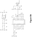
- FIG. 8 A-D Detailed schematics showing electronic circuitry for implementing the disclosure including the examples.
- the eWriter device 800 , 800 ′, 800 ′′ with adjustable select erase of this disclosure includes an optional housing 809 .
- the eWriter display 804 includes substrates 11 spaced apart from each and disposed in the housing.
- a front one of the substrates is formed of a flexible polymeric material and included is an optional back one of the substrates.
- the back substrate may be rigid or flexible.
- the back substrate may be formed of a polymeric material, which is optionally clear and optionally flexible.
- Electrically conductive layers 12 are spaced apart from each other and disposed between the front and back substrates.
- a dispersion layer 23 includes a dispersion of cholesteric liquid crystal material and polymer and is disposed between the electrically conductive layers.
- Spacers or other structure maintains a gap between the electrically conductive layers.
- An optional light absorbing layer 19 , 19 ′ absorbs light passing through the dispersion layer 23 . While the layers or components of the eWriter, including one or both of the substrates, coatings on them and the electrically conductive layers, may be optically clear, this does not indicate the need for a precise degree of transparency. The eWriter is designed so that certain layers or components, or all layers or components, are see-through. Pressure applied to the upper substrate using a stylus or fingernail changes a reflectance of the cholesteric liquid crystal material forming an image.
- Electronic circuitry 840 , 840 ′ and 840 ′′ is disposed in the housing ( FIGS.
- a select erase actuator (at least one of switches 806 - 808 , 815 and optionally 805 or 820 of FIGS. 5-7 ) is included in the electronic circuitry and enables a user to adjust the select erase voltage waveform (e.g., increase or decrease the amplitude or voltage of the select erase voltage waveform).
- the electronic circuitry applies the adjusted select erase voltage waveform to the electrically conductive layers to adjust the selective erasing of the image.
- the electronic circuitry of the eWriter is described in more detail below with regard to FIGS. 5-7 and FIG. 8A-D .
- the dispersion layer 23 of the eWriter can include a blend of polymerizable monomer, crosslinker, photoinitiator, nonpolymerizable cholesteric liquid crystal and spacers.
- the dispersion layer can be phase separated into an open celled cholesteric liquid crystal polymer structure in which the liquid crystal can flow when pressure is applied without damaging the polymer structure.
- the chemistry of the dispersion can be similar to that in U.S. Pat. No. 8,228,301.
- the optional housing 809 can also be referred to as a bezel and can contain the components of the eWriter including the electronic circuitry and eWriter display.
- the housing can be in the shape of a frame around the eWriter display and provides a way for securing the at least one actuator for user adjustment.
- the housing ruggedizes the eWriter. Variations of the eWriter may not employ a typical housing, for example, the eWriter can be partially or fully encased in a polymeric material, for example, a rigid clear polymer, and having the actuators in electrical contact with the electrical circuitry but accessible to the user through the polymer. Rather than containing all components in a housing, the eWriter may have the circuitry constructed and arranged differently than in a housing, for example, in a separate layer or segment of the device.
- the light absorbing layer 19 is disposed more distal from the user than the dispersion layer 23 is from the user and absorbs light passing through the dispersion layer.
- This layer 19 can be a color or dark (e.g., black) and is opaque. When layer 19 is dark and the eWriter is placed in the focal conic initial texture, the eWriter appears dark.
- a semitransparent back layer 19 ′ that absorbs light from the dispersion layer can be disposed more distal from the user than the dispersion layer 23 is from the user.
- the semitransparent back layer 19 ′ can be used with or without a back substrate that is disposed below the dispersion layer.
- a suitable semitransparent back layer is described in U.S. Pat. No. 9,116,379, entitled “Electronic Display with Semitransparent Back Layer,” which is incorporated herein by reference in its entirety.
- the semitransparent back layer 19 ′ can provide suitable contrast to the liquid crystal writing device or eWriter while permitting articles behind the eWriter to be seen.
- the semitransparent back layer 19 ′ absorbs light that passes through the dispersion layer 23 , reflects grey light or light of a color and is light transmitting.
- the semitransparent back layer 19 ′ can form a bottom surface of the eWriter, or a semitransparent or clear layer can be disposed below the semitransparent back layer and forms a bottom surface of the eWriter.
- the eWriter device 800 , 800 ′, 800 ′′ may be used with a back pattern that is removably disposed behind the semitransparent back layer, wherein the pattern is visible through the semitransparent back layer 19 ′.
- the back pattern can comprise a waveguide including light sources disposed at an edge thereof, and light emitting portions on a surface of the waveguide enabling light to leave the waveguide in a pattern.
- the back pattern can comprises an emissive, backlit or reflective display device for displaying images.
- the back pattern can be selected from the group consisting of: a template of a sports field, court or arena, a pattern for a children's game, an image for children to color, notepad lines, graph paper lines, and a menu of items that one can choose from.
- This back pattern may be able to be detachably affixed to the bottom of the eWriter.
- the eWriter is adapted to be placed over a variety of articles for viewing, the articles being free of attachment to the display.
- the semitransparent back layer 19 ′ may comprise ink or pigment coated or printed on, or disposed inside, a transparent substrate. It may also be in the form of a color filter.
- the eWriter device 800 , 800 ′, 800 ′′ can be written on with any suitable stylus 16 or with a fingernail.
- the stylus 16 can be a pointed object made of plastic or other suitable material that does not leave ink on the display when writing.
- the same pointed end of the stylus 16 , or a more blunt eraser end of the stylus 16 can be used as an eraser for select erasing.
- the eraser may be formed of the same or a different material than the stylus.
- the stylus 16 could be formed of polymer having a pointed tip at one end while at the other end an eraser is disposed, formed of a softer polymer, for example, a softer synthetic polymer or rubber.
- An eraser completely separate from the stylus and eWriter could also be used for select erase, having any desired shape.
- a liquid crystal eWriter device 800 includes an eWriter display or writing surface 804 , and associated electronic circuitry 840 .
- the circuitry includes a processor 801 , bias circuit 830 , eWriter drive circuit 803 and a battery 802 as the power supply for the electronic circuitry.
- the processor 801 may be a general purpose microcontroller such as a member of the MSP430 or Tiva families from Texas Instruments.
- the battery connects directly to the linear regulator 850 to generate the logic power VCC and also connects to the bias circuit 830 .
- the logic power VCC from the linear regulator is received by the components of the device as indicated in the drawings. In cases where the battery directly supplies a voltage suitable for use as the logic power VCC, for example in the case of powering the device from a 3V coin cell, the linear regulator may be removed and VBAT connected directly to VCC.
- the electronic circuitry 840 of the eWriter of FIG. 5 includes five switches or actuators: a FULL ERASE switch 805 , a SELECT ERASE switch 806 , a voltage UP switch 807 (e.g., or a select erase UP switch when the select erase waveform is changed by frequency or duty cycle), a voltage DOWN switch 808 (e.g., or a select erase DOWN switch when the select erase waveform is changed by frequency or duty cycle) and a LOCK switch 820 that when activated prevents the Full Erase Switch from fully erasing the image.
- SELECT ERASE actuators include the SELECT ERASE switch 806 , the UP switch 807 and the DOWN switch 808 , enabling user adjustment of select erase.
- the image on the eWriter 800 is fully erased by voltage pulses or a voltage waveform of continuous pulses supplied by the drive circuit 803 as disclosed for example, in the U.S. Pat. No. 8,139,039 patent.
- select erase voltage pulses are also described in the U.S. Pat. No. 8,139,039 patent, this patent does not describe an eWriter with user adjustable select erase.
- the eWriter device 800 of this example is a large format eWriter that is operated in Mode B.
- the FULL ERASE switch is pressed by the user to erase the entire device to the focal conic (dark) texture.
- the focal conic texture is substantially transparent and reveals a dark or color back layer or a semitransparent back layer.
- the user writes on the display using a stylus, with the device displaying the planar (bright) texture where it has been written on.
- the stylus can be composed of polymer or other material with a pointed tip and does not leave ink on the writing/drawing surface. Pressing the SELECT ERASE switch puts the device in SELECT ERASE MODE.
- a fingernail, the stylus or similar instrument is used to apply pressure (select erase pressure) to the eWriter while tracing a portion of the image, partially erasing the display to the focal conic (dark) texture where the pressure is applied.
- the processor 801 adjusts the RMS voltage of the select erase waveform up or down by configuring the bias circuit 830 to provide a DC voltage of the desired waveform amplitude to the drive circuit 803 .
- the bias circuit 830 may be configured to output a fixed DC voltage and the processor 801 adjusts the RMS voltage of the select erase waveform by configuring the drive circuit 803 to vary the duty cycle of the applied pulses.
- the bias circuit 830 may be configured to output a fixed DC voltage and the processor 801 adjusts the RMS voltage of the select erase waveform by configuring the drive circuit 803 to vary the frequency of the applied pulses, relying on RC effects to lower the RMS voltage as frequency is increased.
- the user may adjust the voltage of the select erase voltage waveform down if they notice that written lines which are to be retained are dimming, without select erase pressure being applied.
- the user may adjust the voltage of the select erase waveform up if they notice that lines they are trying to selectively erase are not able to be erased or require excessive pressure to erase. Pressing the SELECT ERASE switch again disables the SELECT ERASE MODE.
- the UP and DOWN switches may produce differing effects based upon the manner in which they are applied. For instance, a single-click feature may adjust the voltage of the select erase waveform up or down by a small amount, for example, by a voltage increment ranging from 50 mV to 250 mV, while a double-click feature may adjust the voltage of the select erase waveform up or down by a relatively larger amount, for example, by a voltage increment of 1V to 2V.
- the small voltage adjustments and larger voltage adjustments can be preset when programming the processor. This provides a mechanism for the user to quickly make large scale or fine scale adjustments.
- the adjustable range of the applied voltage for select erase may be limited, for instance, between 2V and 10V.
- the eWriter device 800 may optionally include an LED or other lighting component 845 .
- the LED may indicate when the applied select erase voltage level is changed via pressing the UP or DOWN switches to provide feedback to the user that the intent was registered. This indication by the lighting component may include different light pulsing, a different color, or other indication to distinguish that one or the other of the UP switch or DOWN switch is being pressed.
- one LED could be one color (e.g., red) for indicating voltage down and another LED could be a different color (e.g., green) for indicting voltage up.
- the LED could pulse quickly when applying the feature for larger voltage adjustments (e.g., the double click feature) and could pulse slowly for small voltage adjustments (e.g., the single click feature). This is desirable because the immediate visual effect of making small changes to the applied voltage level can be subtle.
- LED or other lighting components can be used in any of the other embodiments of this disclosure, including in the examples below.
- FIG. 6 A general design block diagram of an example embodiment is shown in FIG. 6 where like reference numbers represent the same or similar elements with regard to FIG. 5 .
- It includes an eWriter device 800 ′ including an eWriter display or writing surface 804 and associated electronic circuitry 840 ′.
- the circuitry includes a processor 801 , bias circuit 830 , eWriter drive circuit 803 and a battery 802 as the power supply for the electronic circuitry.
- the processor may be a general purpose microcontroller such as a member of the MSP430 or Tiva families from Texas Instruments.
- the image on the eWriter 800 ′ is fully erased by voltage pulses or a waveform of continuous pulses supplied by the drive circuit 803 as disclosed for example, in the U.S. Pat. No. 8,139,039 patent.
- the letter-sized eWriter writing surface 804 is operated in Mode B.
- the FULL ERASE switch is pressed by the user to erase the entire device to the initial focal conic (e.g., dark) texture as background.
- the user writes on the display using a stylus, with the device displaying the planar (bright) color texture where it has been written on, which contrasts with the dark background.
- Pressing the SELECT ERASE switch puts the device in SELECT ERASE MODE continuously while the switch is pressed by the user, while releasing the SELECT ERASE switch disables the SELECT ERASE MODE.
- the stylus or similar instrument is used to apply select erase pressure to the eWriter by tracing over a portion of the image, partially erasing the display to the focal conic (dark) texture where the select erase pressure is applied and while the select erase voltage waveform is applied.
- the select erase voltage waveform is a 10 Hz square wave that oscillates between +/ ⁇ 3.8V.
- the waveform also includes a short 125 microsecond interval that discharges to 0V before changing polarity (from +3.8V to ⁇ 3.8V or vice versa) as a power-saving mechanism.
- the voltage of the select erase voltage waveform may be tuned between 2V and 7V by the user.
- the current select erase voltage waveform is remembered and reused from one select erase to the next; however, it may revert to the default if the system is reset.
- the user may tune the select erase voltage only while the SELECT ERASE switch is pressed.
- a particular method is to press the FULL ERASE switch while in SELECT ERASE MODE to perform the select erase tuning.
- the current select erase voltage is retained from the most recent previous select erase using values stored in a memory (for example register, RAM, EEPROM, or flash) of the processor 801 . If the user wishes to adjust or tune the voltage of the applied select erase voltage waveform, they single-click the FULL ERASE switch while the SELECT ERASE switch is pressed. This first click resets the current select erase waveform voltage to the minimum (2V) level.
- the SELECT ERASE actuators include the SELECT ERASE switch and the FULL ERASE switch when applied simultaneously with the SELECT ERASE switch, enabling the user to adjust select erasing.
- the user applies select erase pressure while tracing over a portion (e.g., a portion of a line) of the image and observes the effect.
- the user can increase a voltage of the select erase waveform, apply select erase pressure while tracing over the line and observe the effect again. This can be repeated until the desired select erasing is obtained.
- the user can stop clicking the FULL ERASE switch once the desired select erasing level is achieved. If they go too far, they can disable the SELECT ERASE MODE by releasing the switch and then once again put the device in the SELECT ERASE MODE by pressing the switch again, so that the first click of the FULL ERASE switch will once again reset the current select erase voltage to the minimum (2V) level.
- the LOCK switch In the on position, the LOCK switch prevents the FULL ERASE switch from erasing the display. Depending on the device, the LOCK switch may or may not be designed to also prevent putting the device in SELECT ERASE MODE.
- a single-click of the FULL ERASE switch could be used to decrease the voltage of the select erase waveform one step ( ⁇ 250 mV) while a double-click of the FULL ERASE switch could be used to increase the voltage of the select erase voltage one step ( ⁇ 250 mV).
- An eWriter device 800 ′′ includes an eWriter display or writing surface 804 and associated electronic circuitry 840 ′′.
- the circuitry includes a processor 801 , bias circuit 830 , eWriter drive circuit 803 and a battery 802 as the power supply for the electronic circuitry.
- the processor may be a general purpose microcontroller such as a member of the MSP430 or Tiva families from Texas Instruments.
- the eWriter 800 ′′ is operated in Mode B.
- the eWriter includes two switches or actuators, FULL ERASE switch 805 and SELECT ERASE switch 806 , and a dial or slider actuator 815 .
- the FULL ERASE and SELECT ERASE switches function the same as in EXAMPLE 1.
- a potentiometer includes a rotating or sliding contact.
- the adjustable voltage divider provided by the potentiometer provides a voltage level that may be used to adjust the applied select erase voltage (or possibly duty cycle or frequency of the select erase voltage waveform). In this case, the user turns the dial or slides the slider to produce the same effect as pressing the UP/DOWN switches in EXAMPLE 1.
- the SELECT ERASE actuators include the SELECT ERASE switch and the potentiometer.
- An 8.5′′ eWriter device is operated in Mode B.
- the eWriter includes a single momentary switch or actuator called ERASE.
- a double-click of the ERASE switch causes a full erase of the writing tablet. Pressing and holding the ERASE switch puts the device in SELECT ERASE MODE for the duration the ERASE switch is held.
- a single-click of the ERASE switch followed immediately by a hold enables select erase at decreased voltage.
- a double-click of the ERASE switch followed immediately by a hold enables select erase at increased voltage.
- the single ERASE switch functions as the SELECT ERASE actuator.
- FIGS. 8A-D provide schematics for circuitry suitable to implement the aspects of the disclosure including Examples 1-4.
- a battery for instance 4 AA alkaline batteries connected in series, or other suitable power supply provides a voltage VBAT to power the system.
- a low-dropout linear regulator U1 in this case a Texas Instruments' TPS77033, generates the logic power supply VCC from VBAT.
- a Texas Instruments' MSP430G2553 microcontroller provides the processing for the system. All I/O connected to the microcontroller are digital, with the exception of the POT signal.
- the POT signal is an analog input that may be programmatically configured for measurement by the built-in analog to digital (A/D) converter of the microcontroller.
- standard reset and programming circuitry for the microcontroller including C3, R9, and header J1.
- FIG. 8B provides a series of momentary switches S 1 -S 4 and a toggle switch S 5 .
- the states of these switches are indicated by signals SW_ 1 -SW_ 5 , which are provided to general purpose I/O pins of the microcontroller.
- the microcontroller may use well-known techniques involving interrupts, polling, and debouncing to detect events on the switches resulting from user input.
- a potentiometer W 2 is also included as a means of user input. Through the action of moving a slider or turning a dial, the user may adjust the POT signal between VCC and ground. As previously mentioned, this analog signal is provided to the microcontroller for conversion to a digital value by an internal A/D.
- the digital value represents the setting of the slider or dial as set by a user. Also shown are two LEDs DS 1 and DS 2 which may be turned on programmatically by setting the EN_LED_ 1 and EN_LED_ 2 microcontroller outputs, respectively, to the VCC level.
- FIG. 8C provides a bias circuit for generating an adjustable DC voltage HV on C 12 -C 14 from the VBAT voltage.
- the bias circuit is built around U5, a MAX1771 DC-DC controller from Maxim Integrated.
- L 1 , L 2 , C 11 , C 12 -C 14 , D 1 , and Q 12 are arranged to put the DC-DC controller in a SEPIC configuration.
- a SEPIC single-ended primary-inductor converter
- Voltage level adjustment is provided by U6, an AD5160 from Analog Devices.
- the AD5160 is a 256-Position SPI-Compatible Digital Potentiometer.
- a 1.5V reference is provided to the AD5160 from the MAX1771.
- the microcontroller may use the SPI interface provided by SCK, MOSI, and nCS to set a value D between 0 and 255 in the digital potentiometer.
- the wiper W of the digital potentiometer outputs a voltage equal to (D/256)*1.5V, which is buffered by Texas Instruments' OPA379 op-amp U7 and provided to R 33 .
- the MAX1771 When enabled via the nEN_HV signal from the microcontroller, the MAX1771 regulates the voltage on its feedback input FB to 1.5V via switching action of Q 12 .
- the bias circuit can generate voltages of HV in the range of 3.13V to 41.25V.
- this range can be modified by suitable changes to R 30 , R 32 , and R 33 .
- C 16 serves the purpose of a feedforward capacitor to improve DC-DC converter performance as known in the art.
- the bias circuitry may also be modified to employ a boost converter that integrates features to enable adjusting the output voltage without need of an external digital potentiometer.
- Suitable boost converters are Texas Instruments boost converters: TPS61045 (Digitally Adjustable Boost Converter SLVS440C brochure dated January 2003-Revised December 2014) and TPS61170 (1.2-A High-Voltage Boost Converter in 2-mm ⁇ 2 mm2 QFN package brochure SLVS789D dated November 2007-Revised December 2014), both of which are incorporated herein by reference in their entireties.
- the TPS61045 boost converter demonstrates modifying the boost voltage by using an internal DAC or an analog input to alter the feedback circuit.
- the TPS61170 boost converter allows either a digital interface or pulse width modulation (PWM) input to modify the boost voltage by changing a feedback reference voltage.
- PWM pulse width modulation
- FIG. 8D provides a drive circuit for applying the bias voltage HV generated by the bias circuit to the electrodes 12 , identified individually by signals SEG and COM in FIG. 8D .
- the SEG_L and COM_L signals from the microcontroller enable individually connecting either electrode to ground via a transistor Q 7 or Q 8 and a current-limiting resistor R 12 or R 13 .
- the SEG_H and COM_H signals from the microcontroller enable connecting either electrode to HV via Q 1 or Q 2 and a current-limiting resistor R 7 or R 8 .
- Transistors Q 3 and Q 4 serve the purpose of turning on Q 1 and Q 2 through the voltage drops developed across R 1 and R 2 , respectively.
- R 10 and Q 5 limit the current through R 1 to protect Q 1 from excessive gate to source voltage at high HV levels, while R 11 and Q 6 do the same for R 2 and Q 2 .
Landscapes
- Physics & Mathematics (AREA)
- Nonlinear Science (AREA)
- Chemical & Material Sciences (AREA)
- General Physics & Mathematics (AREA)
- Crystallography & Structural Chemistry (AREA)
- Engineering & Computer Science (AREA)
- Optics & Photonics (AREA)
- Mathematical Physics (AREA)
- Theoretical Computer Science (AREA)
- General Engineering & Computer Science (AREA)
- Dispersion Chemistry (AREA)
- Computer Hardware Design (AREA)
- Human Computer Interaction (AREA)
- Liquid Crystal (AREA)
Abstract
Description
-
- by configuring the bias circuit to provide a DC voltage of a desired waveform amplitude to the drive circuit;
- when the bias circuit is configured to output a fixed DC voltage, by configuring the drive circuit to vary a duty cycle of applied pulses; and
- when the bias circuit is configured to output a fixed DC voltage, by configuring the drive circuit to vary a frequency of applied pulses, relying on RC effects to lower the RMS voltage as frequency is increased.
-
- in a first instance drops the amplitude of the select erase voltage waveform to a minimum level, and
- in subsequent instances successively increases the amplitude of the select erase waveform by a set increment up to a maximum level.
-
- selecting and applying a small increment in the amplitude of said select erase voltage waveform or a larger increment in the amplitude of said select erase voltage waveform, and
- selecting and applying the amplitude of said select erase voltage waveform up or down.
-
- (e1) evaluating whether the image dims while the select erase voltage waveform is applied but the select erase pressure is not applied;
- (e2) if results of step (e1) are positive, then the user adjusts the at least one SELECT ERASE actuator to adjust the select erase voltage waveform to decrease select erasing; and
- optionally repeating any of steps (b)-(d), (e1) and (e2).
Claims (21)
Priority Applications (1)
| Application Number | Priority Date | Filing Date | Title |
|---|---|---|---|
| US16/103,500 US10634939B2 (en) | 2017-08-15 | 2018-08-14 | Selectively erasable eWriter with user adjustment |
Applications Claiming Priority (2)
| Application Number | Priority Date | Filing Date | Title |
|---|---|---|---|
| US201762545874P | 2017-08-15 | 2017-08-15 | |
| US16/103,500 US10634939B2 (en) | 2017-08-15 | 2018-08-14 | Selectively erasable eWriter with user adjustment |
Publications (2)
| Publication Number | Publication Date |
|---|---|
| US20190056611A1 US20190056611A1 (en) | 2019-02-21 |
| US10634939B2 true US10634939B2 (en) | 2020-04-28 |
Family
ID=65361365
Family Applications (1)
| Application Number | Title | Priority Date | Filing Date |
|---|---|---|---|
| US16/103,500 Active 2038-10-27 US10634939B2 (en) | 2017-08-15 | 2018-08-14 | Selectively erasable eWriter with user adjustment |
Country Status (3)
| Country | Link |
|---|---|
| US (1) | US10634939B2 (en) |
| JP (1) | JP6831080B2 (en) |
| CN (1) | CN109407385B (en) |
Families Citing this family (12)
| Publication number | Priority date | Publication date | Assignee | Title |
|---|---|---|---|---|
| CN112241215B (en) * | 2019-07-18 | 2024-01-30 | 南京机器岛智能科技有限公司 | A method for intelligently adjusting the critical voltage of an LCD writing pad |
| CN110703527B (en) * | 2019-09-04 | 2022-11-11 | 陈华丰 | Liquid crystal display device and erasing method thereof |
| US11315434B2 (en) | 2019-10-31 | 2022-04-26 | Rockwell Collins, Inc. | System and method to change SVS mode |
| CN110928445A (en) * | 2019-10-31 | 2020-03-27 | 山东蓝贝思特教装集团股份有限公司 | Local erasing voltage loading control method for liquid crystal writing film |
| CN110727137A (en) * | 2019-11-01 | 2020-01-24 | 重庆洋逸乐科技有限公司 | Message board and message wall capable of being repeatedly used |
| US11097851B1 (en) * | 2019-11-19 | 2021-08-24 | Rockwell Collins, Inc. | System and method to momentarily switch SVS mode |
| CN111124188B (en) * | 2019-12-30 | 2025-04-22 | 广州中基国威电子科技有限公司 | Liquid crystal handwriting tablet driver chip and application circuit thereof, and liquid crystal handwriting tablet |
| CN111240060B (en) * | 2020-03-13 | 2025-06-24 | 青岛诚志光电科技有限公司 | Liquid crystal writing film circuit structure, liquid crystal writing film and liquid crystal writing board |
| US11262635B1 (en) * | 2021-02-05 | 2022-03-01 | Kent Displays, Inc. | Magnet erased eWriter |
| KR102883310B1 (en) * | 2021-05-24 | 2025-11-10 | 삼성디스플레이 주식회사 | Display device |
| CN118675475A (en) * | 2023-03-17 | 2024-09-20 | 群创光电股份有限公司 | Electronic Devices |
| CN117572680B (en) * | 2024-01-16 | 2024-05-14 | 山东蓝贝思特教装集团股份有限公司 | A method and device for controlling partial erasure of a liquid crystal writing device |
Citations (7)
| Publication number | Priority date | Publication date | Assignee | Title |
|---|---|---|---|---|
| US4525032A (en) | 1982-07-27 | 1985-06-25 | The Secretary Of State For Defence In Her Britannic Majesty's Government Of The United Kingdom Of Great Britain And Northern Ireland | Liquid crystal reusable signature comparison |
| US5453863A (en) | 1991-05-02 | 1995-09-26 | Kent State University | Multistable chiral nematic displays |
| US5691795A (en) | 1991-05-02 | 1997-11-25 | Kent State University | Polymer stabilized liquid crystalline light modulating device and material |
| US6104448A (en) | 1991-05-02 | 2000-08-15 | Kent State University | Pressure sensitive liquid crystalline light modulating device and material |
| US8139039B2 (en) | 2007-07-31 | 2012-03-20 | Kent Displays, Incorporated | Selectively erasable electronic writing tablet |
| US8228301B2 (en) | 2007-07-31 | 2012-07-24 | Kent Displays Incorporated | Multiple color writing tablet |
| US9116379B2 (en) | 2012-05-22 | 2015-08-25 | Kent Displays Incorporated | Electronic display with semitransparent back layer |
Family Cites Families (5)
| Publication number | Priority date | Publication date | Assignee | Title |
|---|---|---|---|---|
| JP5692693B2 (en) * | 2009-10-20 | 2015-04-01 | Nltテクノロジー株式会社 | Display medium erasing apparatus and method, and erasing signal setting method |
| TW201333758A (en) * | 2011-11-01 | 2013-08-16 | Kent Displays Inc | Writing tablet information recording device |
| CN106486169B (en) * | 2015-08-24 | 2019-10-18 | 北京兆易创新科技股份有限公司 | A kind of method for deleting of Nand Flash |
| CN105467708B (en) * | 2016-02-03 | 2021-04-20 | 京东方科技集团股份有限公司 | A writing board, electronic writing equipment and production method |
| CN206378662U (en) * | 2017-01-13 | 2017-08-04 | 深圳市好写科技有限公司 | Selective erase liquid crystal display device |
-
2017
- 2017-10-27 JP JP2017208500A patent/JP6831080B2/en active Active
- 2017-11-07 CN CN201711082057.0A patent/CN109407385B/en active Active
-
2018
- 2018-08-14 US US16/103,500 patent/US10634939B2/en active Active
Patent Citations (7)
| Publication number | Priority date | Publication date | Assignee | Title |
|---|---|---|---|---|
| US4525032A (en) | 1982-07-27 | 1985-06-25 | The Secretary Of State For Defence In Her Britannic Majesty's Government Of The United Kingdom Of Great Britain And Northern Ireland | Liquid crystal reusable signature comparison |
| US5453863A (en) | 1991-05-02 | 1995-09-26 | Kent State University | Multistable chiral nematic displays |
| US5691795A (en) | 1991-05-02 | 1997-11-25 | Kent State University | Polymer stabilized liquid crystalline light modulating device and material |
| US6104448A (en) | 1991-05-02 | 2000-08-15 | Kent State University | Pressure sensitive liquid crystalline light modulating device and material |
| US8139039B2 (en) | 2007-07-31 | 2012-03-20 | Kent Displays, Incorporated | Selectively erasable electronic writing tablet |
| US8228301B2 (en) | 2007-07-31 | 2012-07-24 | Kent Displays Incorporated | Multiple color writing tablet |
| US9116379B2 (en) | 2012-05-22 | 2015-08-25 | Kent Displays Incorporated | Electronic display with semitransparent back layer |
Also Published As
| Publication number | Publication date |
|---|---|
| JP2019035931A (en) | 2019-03-07 |
| CN109407385A (en) | 2019-03-01 |
| US20190056611A1 (en) | 2019-02-21 |
| JP6831080B2 (en) | 2021-02-17 |
| CN109407385B (en) | 2022-08-30 |
Similar Documents
| Publication | Publication Date | Title |
|---|---|---|
| US10634939B2 (en) | Selectively erasable eWriter with user adjustment | |
| US8228301B2 (en) | Multiple color writing tablet | |
| US8139039B2 (en) | Selectively erasable electronic writing tablet | |
| US10558065B2 (en) | Liquid crystal writing device with slow discharge erase | |
| US20100265214A1 (en) | Writing tablet information recording device | |
| US9946106B2 (en) | Electronic display with semitransparent back layer | |
| CN101828143B (en) | Display device having dot-matrix display element and driving method thereof | |
| US9927672B2 (en) | Multicolored pressure sensitive liquid crystal device | |
| US10287503B2 (en) | Enhanced brightness eWriter device | |
| JP2005516378A (en) | Thin planar switch and its application | |
| US20130314621A1 (en) | Electronic display with patterned layer | |
| CN113759623B (en) | Liquid crystal writing board, display method and writing device thereof | |
| TW201340083A (en) | Cholesteric liquid crystal display device and method for controlling drive of cholesteric liquid crystal display element | |
| CN113917754B (en) | Liquid crystal handwriting device and display method thereof | |
| KR101773950B1 (en) | Display device and driving method thereof | |
| CN102456314A (en) | Display device and electronic apparatus having the same | |
| JP2019078979A (en) | Display and driving method | |
| JP2013503367A (en) | Rapid migration of large area cholesteric displays | |
| US11698563B2 (en) | Cholesteric liquid crystal writing device with stylus erase | |
| CN1322338A (en) | Unipolar driving of bistable cholesteric liquid crystal display | |
| CN107680553B (en) | Gray-scale display segment code liquid crystal screen and gray-scale display method thereof | |
| JP5143417B2 (en) | Electrophoretic display device, control device, control method, and display system | |
| KR20070019714A (en) | Electrophoretic display with fast drawing mode waveforms | |
| Lee et al. | P‐89: A Novel Dynamic Drive Scheme for Reflective Cholesteric Displays |
Legal Events
| Date | Code | Title | Description |
|---|---|---|---|
| FEPP | Fee payment procedure |
Free format text: ENTITY STATUS SET TO UNDISCOUNTED (ORIGINAL EVENT CODE: BIG.); ENTITY STATUS OF PATENT OWNER: LARGE ENTITY |
|
| AS | Assignment |
Owner name: KENT DISPLAYS INC., OHIO Free format text: ASSIGNMENT OF ASSIGNORS INTEREST;ASSIGNORS:MARHEFKA, DUANE;BRAGANZA, CLINTON I.;REEL/FRAME:046641/0289 Effective date: 20171128 |
|
| STPP | Information on status: patent application and granting procedure in general |
Free format text: DOCKETED NEW CASE - READY FOR EXAMINATION |
|
| STPP | Information on status: patent application and granting procedure in general |
Free format text: NOTICE OF ALLOWANCE MAILED -- APPLICATION RECEIVED IN OFFICE OF PUBLICATIONS |
|
| STCF | Information on status: patent grant |
Free format text: PATENTED CASE |
|
| MAFP | Maintenance fee payment |
Free format text: PAYMENT OF MAINTENANCE FEE, 4TH YEAR, LARGE ENTITY (ORIGINAL EVENT CODE: M1551); ENTITY STATUS OF PATENT OWNER: LARGE ENTITY Year of fee payment: 4 |
|
| AS | Assignment |
Owner name: BUFFALO GAMES, LLC, NEW YORK Free format text: ASSIGNMENT OF ASSIGNORS INTEREST;ASSIGNOR:KENT DISPLAYS, INC.;REEL/FRAME:070552/0114 Effective date: 20250307 |
|
| AS | Assignment |
Owner name: U.S. BANK NATIONAL ASSOCIATION, MINNESOTA Free format text: SECURITY INTEREST;ASSIGNORS:BUFFALO GAMES, LLC;EASTPOINT SPORTS LTD., LLC;WILD SALES, LLC;REEL/FRAME:071475/0258 Effective date: 20250602 |