US10634848B2 - Optical filter and optical transmission device - Google Patents
Optical filter and optical transmission device Download PDFInfo
- Publication number
- US10634848B2 US10634848B2 US16/425,131 US201916425131A US10634848B2 US 10634848 B2 US10634848 B2 US 10634848B2 US 201916425131 A US201916425131 A US 201916425131A US 10634848 B2 US10634848 B2 US 10634848B2
- Authority
- US
- United States
- Prior art keywords
- light
- face
- optical
- spectrum
- optical filter
- Prior art date
- Legal status (The legal status is an assumption and is not a legal conclusion. Google has not performed a legal analysis and makes no representation as to the accuracy of the status listed.)
- Expired - Fee Related
Links
Images


Classifications
-
- G—PHYSICS
- G02—OPTICS
- G02B—OPTICAL ELEMENTS, SYSTEMS OR APPARATUS
- G02B6/00—Light guides; Structural details of arrangements comprising light guides and other optical elements, e.g. couplings
- G02B6/24—Coupling light guides
- G02B6/26—Optical coupling means
- G02B6/28—Optical coupling means having data bus means, i.e. plural waveguides interconnected and providing an inherently bidirectional system by mixing and splitting signals
- G02B6/293—Optical coupling means having data bus means, i.e. plural waveguides interconnected and providing an inherently bidirectional system by mixing and splitting signals with wavelength selective means
- G02B6/29304—Optical coupling means having data bus means, i.e. plural waveguides interconnected and providing an inherently bidirectional system by mixing and splitting signals with wavelength selective means operating by diffraction, e.g. grating
- G02B6/29305—Optical coupling means having data bus means, i.e. plural waveguides interconnected and providing an inherently bidirectional system by mixing and splitting signals with wavelength selective means operating by diffraction, e.g. grating as bulk element, i.e. free space arrangement external to a light guide
- G02B6/29311—Diffractive element operating in transmission
-
- G—PHYSICS
- G02—OPTICS
- G02B—OPTICAL ELEMENTS, SYSTEMS OR APPARATUS
- G02B6/00—Light guides; Structural details of arrangements comprising light guides and other optical elements, e.g. couplings
- G02B6/24—Coupling light guides
- G02B6/26—Optical coupling means
- G02B6/34—Optical coupling means utilising prism or grating
-
- G—PHYSICS
- G02—OPTICS
- G02B—OPTICAL ELEMENTS, SYSTEMS OR APPARATUS
- G02B6/00—Light guides; Structural details of arrangements comprising light guides and other optical elements, e.g. couplings
- G02B6/24—Coupling light guides
- G02B6/26—Optical coupling means
- G02B6/262—Optical details of coupling light into, or out of, or between fibre ends, e.g. special fibre end shapes or associated optical elements
-
- G—PHYSICS
- G02—OPTICS
- G02B—OPTICAL ELEMENTS, SYSTEMS OR APPARATUS
- G02B6/00—Light guides; Structural details of arrangements comprising light guides and other optical elements, e.g. couplings
- G02B6/24—Coupling light guides
- G02B6/42—Coupling light guides with opto-electronic elements
- G02B6/4201—Packages, e.g. shape, construction, internal or external details
- G02B6/4204—Packages, e.g. shape, construction, internal or external details the coupling comprising intermediate optical elements, e.g. lenses, holograms
- G02B6/4215—Packages, e.g. shape, construction, internal or external details the coupling comprising intermediate optical elements, e.g. lenses, holograms the intermediate optical elements being wavelength selective optical elements, e.g. variable wavelength optical modules or wavelength lockers
-
- G—PHYSICS
- G02—OPTICS
- G02B—OPTICAL ELEMENTS, SYSTEMS OR APPARATUS
- G02B6/00—Light guides; Structural details of arrangements comprising light guides and other optical elements, e.g. couplings
- G02B6/24—Coupling light guides
- G02B6/26—Optical coupling means
- G02B6/28—Optical coupling means having data bus means, i.e. plural waveguides interconnected and providing an inherently bidirectional system by mixing and splitting signals
- G02B6/293—Optical coupling means having data bus means, i.e. plural waveguides interconnected and providing an inherently bidirectional system by mixing and splitting signals with wavelength selective means
- G02B6/29304—Optical coupling means having data bus means, i.e. plural waveguides interconnected and providing an inherently bidirectional system by mixing and splitting signals with wavelength selective means operating by diffraction, e.g. grating
- G02B6/29305—Optical coupling means having data bus means, i.e. plural waveguides interconnected and providing an inherently bidirectional system by mixing and splitting signals with wavelength selective means operating by diffraction, e.g. grating as bulk element, i.e. free space arrangement external to a light guide
- G02B6/29313—Optical coupling means having data bus means, i.e. plural waveguides interconnected and providing an inherently bidirectional system by mixing and splitting signals with wavelength selective means operating by diffraction, e.g. grating as bulk element, i.e. free space arrangement external to a light guide characterised by means for controlling the position or direction of light incident to or leaving the diffractive element, e.g. for varying the wavelength response
-
- G—PHYSICS
- G02—OPTICS
- G02B—OPTICAL ELEMENTS, SYSTEMS OR APPARATUS
- G02B6/00—Light guides; Structural details of arrangements comprising light guides and other optical elements, e.g. couplings
- G02B6/24—Coupling light guides
- G02B6/26—Optical coupling means
- G02B6/35—Optical coupling means having switching means
- G02B6/351—Optical coupling means having switching means involving stationary waveguides with moving interposed optical elements
- G02B6/3512—Optical coupling means having switching means involving stationary waveguides with moving interposed optical elements the optical element being reflective, e.g. mirror
Definitions
- the embodiments discussed herein are related to an optical filter and an optical transmission device.
- An optical filter is a device for selectively allowing light having a particular wavelength to transmit.
- the optical filter is a device incorporated into optical transmission devices and the like and therefore, is demanded to be reduced in size according to the trends of the times.
- a wavelength selectable switch used in building an optical multiplexing communication system also functions as the optical filter.
- the wavelength selectable switch is a device that selects signal light having a particular wavelength from a wavelength-multiplexed input signal using a diffraction grating, and outputs the selected signal light through one of a plurality of output fibers. Accordingly, by using only one of the plurality of output fibers, the wavelength selectable switch functions as the optical filter.
- the preferred transmission characteristic of the optical filter is a filtering characteristic that the transmittance is high in a certain wavelength range (for example, 1 dB band), and suddenly decreases on the both sides of the wavelength range.
- the Gaussian filtering characteristic into a desired filtering characteristic (that is, filtering characteristic that the transmittance suddenly decreases on both sides of a wavelength range) by providing a slit plate between the diffraction grating of the wavelength selectable switch and the output fiber.
- the slit plate makes downsizing of the variable-wavelength filter difficult.
- the downsizing of the optical filter including the variable-wavelength filter follows the trends of the times, such hard-to-downsize optical filter is unpractical.
- an optical filter includes a spectroscopic element configured to disperse input light, and emit the dispersed input light as spectrum light; and an optical fiber including an end face having a recess, a core having a first face in contact with a bottom of the recess and a second face sandwiched between the first face and a circumference end of the recess, and a clad surrounding the core, wherein in the optical fiber, the recess is irradiated with the spectrum light, the second face is inclined such that a second portion incident from the second face to the core out of the irradiated spectrum light is emitted to the clad, and a first portion incident from the first face to the core out of the irradiated spectrum light is outputted.
- FIG. 1 is a view illustrating an example of the configuration of an optical filter in accordance with Embodiment 1;
- FIG. 2 is a view illustrating an example of the configuration of the optical filter in accordance with Embodiment 1;
- FIG. 3 is a view illustrating an example of the configuration of the optical filter in accordance with Embodiment 1;
- FIG. 4 is a view illustrating an example of the configuration of the optical filter in accordance with Embodiment 1;
- FIG. 5 is a view illustrating an example of spectrum light projected onto a recess
- FIG. 6 is a view illustrating an optical path of the spectrum light in an output fiber
- FIG. 7 is a view for describing an example of the spectrum light on an end face of the output fiber
- FIG. 8 is a view illustrating an example of a transmission characteristic of the optical filter
- FIG. 9 is a view for describing conditions for emission of a spectrum end portion to a clad
- FIG. 10 is a view illustrating an example of an output of an EDFA
- FIGS. 11A and 11B are views for describing an example of input light travelling in an input fiber
- FIGS. 12A and 12B are views for describing an example of the input light immediately after emission from the input fiber
- FIGS. 13A and 13B are views for describing an example of the input light travelling between the input fiber and the lens
- FIGS. 14A and 14B are views for describing an example of the spectrum light on the mirror
- FIGS. 15A and 15B are views for describing an example of the spectrum light on the end face of the output fiber
- FIGS. 16A and 16B are views for describing an example of the spectrum light in the output fiber
- FIG. 17 is a view illustrating an example of the configuration of optical filter that is different from the optical filter in FIG. 1 in configuration;
- FIGS. 18A and 18B are views for describing an example of input light immediately after emission from the input fiber
- FIGS. 19A and 19B are views for describing an example of the input light traveling between the input fiber and the lens
- FIGS. 20A and 20B are views for describing an example of spectrum light on a mirror
- FIGS. 21A and 21B are views for describing an example of the spectrum light on the end face of the output fiber
- FIGS. 22A and 22B are views for describing an example of the spectrum light traveling in the output fiber
- FIG. 23 is a view illustrating an example of the configuration of optical filter that is different from the optical filter in FIG. 1 in configuration;
- FIG. 24 is a view for describing a modification example of Embodiment 1;
- FIG. 25 is a view illustrating the operation of the reflection part
- FIG. 26 is a view illustrating an example of the hardware configuration of the reflection part
- FIG. 27 is a view illustrating an example of a MEMS mirror
- FIG. 28 is a view illustrating an example of the operation of the MEMS mirror
- FIG. 29 is a view illustrating an example of the configuration of an ASIC
- FIG. 30 is a view illustrating an example of a look-up table
- FIG. 31 is a view illustrating an example of the configuration of an output fiber in an optical filter in accordance with Embodiment 2;
- FIG. 32 is a view for deriving an area where the spectrum light projected onto the recess is emitted to the clad
- FIG. 33 is a view for describing an example of a method of finding an area where a light beam is emitted to the clad
- FIG. 34 is a view illustrating an example of the configuration of an output fiber in an optical filter in accordance with Embodiment 3;
- FIG. 35 is a view illustrating an example of the configuration of the output fiber in the optical filter in accordance with Embodiment 3;
- FIG. 36 is a view illustrating an example of the configuration of an optical transmission device in accordance with Embodiment 4.
- FIG. 37 is a view for describing an example of the operation of the optical transmission device.
- FIG. 38 is a view illustrating an example of the hardware configuration of a light source part
- FIGS. 39A and 39B are views illustrating an example of look-up tables
- FIG. 40 is a view illustrating an example of the hardware configuration of a modulation part
- FIG. 41 is a view illustrating an example of the hardware configuration of an optical amplification part
- FIG. 42 is a view illustrating an example of the configuration of the ASIC
- FIG. 43 is a view illustrating an example of a look-up table
- FIG. 44 is a view illustrating an example of the hardware configuration of a monitor part
- FIG. 45 is a view illustrating an example of the hardware configuration of a control part
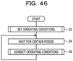
- FIG. 46 is a view illustrating an example of a flow chart of a control program
- FIG. 47 is a flow chart of an example of a subprocess illustrating details in Step S 2 ;
- FIG. 48 is a flow chart of an example of a subprocess illustrating details in Step S 6 ;
- FIG. 49 is a view illustrating an example of a device using the optical transmission device.
- FIG. 50 is a view illustrating the flow of signal light in a ROADM
- FIG. 51 is a view illustrating the configuration and operation of each block of the ROADM
- FIG. 52 is a view for describing an example of noise characteristics of second signal light beam.
- FIG. 53 is a view for describing an example of noise characteristics of the second signal light beams in the case where the optical filters of a plurality of optical transmission devices each are replaced with the optical filter described with reference to FIG. 17 .
- FIGS. 1 to 4 are views illustrating an example of the configuration of an optical filter 2 in accordance with Embodiment 1.
- the optical filter 2 has a spectroscopic part 4 and an optical fiber 6 (hereinafter referred to as output fiber).
- the spectroscopic part 4 (see FIG. 4 ) disperses input light 8 , and emits dispersed input light 10 (hereinafter referred to as spectrum light).
- the spectroscopic part 4 has, for example, an optical fiber 5 (hereinafter referred to as input fiber) and a lens 7 .
- the input fiber 5 is, for example, an optical fiber stored in a ferrule (this also applies to the output fiber 6 ).
- the spectroscopic part 4 further has a diffraction grating 9 and a mirror 11 .
- the input fiber 5 is, for example, a single mode fiber having a recess 112 on its end face.
- the input fiber 5 has the same configuration as the output fiber 6 .
- the end face of the input fiber 5 may be a flat end face having no recess 112 .
- the spectrum light 10 is filtered by the output fiber 6 , there is no problem even when the end face of the input fiber 5 is flat.
- the diffraction grating 9 is, for example, a transmission diffraction grating configured such that two types of transparent films having different refractive indexes are alternately stacked on a front face.
- the diffraction grating 9 may be a transmission diffraction grating configured such that cyclic irregularities are formed on a rear face of a transparent substrate.
- the input light 8 is emitted to free space in the spectroscopic part 4 via the input fiber 5 . Then, the input light 8 is converted into a collimated beam by the lens 7 . The input light converted into the collimated beam is dispersed by the diffraction grating 9 . That is, the diffraction grating 9 causes a plurality of components having different wavelengths (hereinafter referred to as wavelength components) included in the input light 8 to travel in different directions.
- the dispersed input light that is, spectrum light
- the dispersed input light includes a plurality of wavelength components travelling in different directions.
- the spectrum light 10 is projected onto the mirror 11 .
- the mirror 11 reflects the spectrum light 10 , and irradiates the diffraction grating 9 with the reflected light.
- the diffraction grating 9 disperses the spectrum light 10 again, and irradiates the lens 7 with the spectrum light 10 .
- the lens 7 condenses the spectrum light 10 , and irradiates the end face of the output fiber 6 with the spectrum light 10 .
- the spectroscopic part 4 may have another spectroscopic element such as a prism in place of the diffraction grating 9 .
- FIG. 2 illustrates a vertical cross section of the output fiber 6 (cross section including the center axis of the output fiber 6 ).
- the output fiber 6 includes an end face 14 having a recess 12 .
- the output fiber 6 further includes a core 16 and a clad 18 that surrounds the core 16 .
- the output fiber 6 is, for example, a single mode fiber.
- FIG. 3 illustrates the end face 14 of the output fiber 6 .
- the core 16 has a first face 22 a that is in contact with a bottom 20 of the recess 12 (see FIG. 2 ) (see FIGS. 2 and 3 ).
- the core 16 further has a second face 22 b sandwiched between the first face 22 a and a circumferential end 24 of the recess 12 .
- the second face 22 b is inclined with respect to a transverse direction 28 of the core 16 (see FIG. 2 , the direction that is perpendicular to the center axis of the core 16 ).
- the recess 12 is irradiated with the spectrum light 10 .
- FIG. 5 is a view illustrating an example of the spectrum light 10 projected onto the recess 12 .
- the second face 22 b (see FIG. 3 ) is inclined with respect to the transverse direction 28 of the core 16 such that a second portion 26 b of the projected spectrum light 10 (see FIG. 5 ), which is incident from the second face 22 b onto the core 16 , is emitted to the clad 18 .
- FIG. 6 is a view illustrating an optical path of the spectrum light 10 in the output fiber 6 .
- FIG. 6 illustrates a first light beam 30 a that travels the center of the spectrum light 10 and a second light beam 30 b that travels a position shifted from the center.
- FIG. 6 further illustrates a third light beam 30 c that travels on the outermost side of the spectrum light 10 .
- the first light beam 30 a illustrates a course of a portion 26 a (see FIG. 5 ; hereinafter referred to as first portion or spectrum center portion) of the spectrum light 10 (see FIG. 5 ), which is incident from the first face 22 a (see FIG. 2 ) onto the core 16 .
- a spectrum center portion 26 a represented by the first light beam 30 a travels in a longitudinal direction 32 of the output fiber 6 (that is, direction that is parallel to an optical axis of the output fiber 6 ).
- the spectrum center portion 26 a may travel in the direction that is inclined with respect to the longitudinal direction 32 to a certain extent.
- the spectrum center portion 26 a is totally reflected on a boundary face 34 between the core 16 and the clad 18 (see FIG. 6 ). That is, the spectrum center portion 26 a travels in the core 16 .
- the second light beam 30 b illustrates a course of the second portion 26 b of the spectrum light 10 (see FIG. 5 ) (hereinafter referred to as spectrum end portion), which is incident from the second face 22 b (see FIG. 2 ) onto the core 16 .
- spectrum end portion a portion of a spectrum end portion 26 b refracts on the boundary face 34 between the core 16 and the clad 18 , and is emitted to the clad 18 .
- the range of the inclination angle of the second face 22 b will be described later.
- the other portion of the spectrum end portion 26 b is reflected on the boundary face 34 .
- the portion reflected on the boundary face 34 is refracted and reflected on the opposite boundary face 34 .
- the spectrum end portion 26 b is gradually emitted to the clad 18 while being repeatedly refracted and reflected on the boundary face 34 .
- the third light beam 30 c illustrates a course of a portion 26 c of the spectrum light 10 (see FIG. 5 ) (hereinafter referred to as spectrum outermost portion), which is directly incident upon the clad 18 .
- the spectrum outermost portion 26 c travels in the clad 18 , and disappears soon.
- the first portion 26 a of the spectrum light 10 which is incident from the first face 22 a (see FIG. 2 ) onto the core 16 is outputted from the output fiber 6 .
- the spectrum outermost portion 26 c represented by the third light beam 30 c travels in the longitudinal direction 32 of the output fiber 6 .
- the spectrum outermost portion 26 c may travel while inclining toward the core 16 to some extent. In this case, a part of the spectrum outermost portion 26 c is incident onto the core 16 and however, the amount of the incident light is small (for example, one-a few hundredth).
- the portion of the spectrum light 10 which is outputted from the optical filter 2 , is only the spectrum center portion 26 a projected onto the first face 22 a (that is, the bottom 20 of the recess 12 ).
- FIG. 7 is a view illustrating an example of the spectrum light 10 on the end face 14 of the output fiber 6 .
- the spectrum light 10 projected onto the recess 12 extends along one axis 33 (hereinafter referred to as wavelength axis) on the end face 14 .
- the wavelength of the spectrum light 10 gradually increases from one end (for example, lower end) toward the other end (for example, upper end) of the wavelength axis 33 .
- the wavelength of the spectrum light 10 is fixed on the axis (hereinafter referred to as spectrum axis) that is perpendicular to the wavelength axis 33 . That is, the wavelength components of the spectrum light 10 are projected onto respective spectrum axes.
- the wavelength of a spectrum axis 36 a that is in contact with the lower end of the first face 22 a is defined as ⁇ 1.
- the wavelength of a spectrum axis 36 b that is in contact with the upper end of the first face 22 a is defined as ⁇ 2 (>1). That is, the wavelength range of the spectrum center portion 26 a is defined as ⁇ 1 to ⁇ 2 ( ⁇ 1 or more and ⁇ 2 or less).
- the spectrum center portion 26 a is outputted from the optical filter 2 substantially as it is. Accordingly, the portion of the input light 8 , which is outputted from the optical filter 2 is a portion having the wavelength in the range of ⁇ 1 to ⁇ 2. In other words, the optical filter 2 allows the portion having the wavelength in the range of ⁇ 1 to ⁇ 2 in the input light 8 to transmit.
- FIG. 8 is a view illustrating an example of a transmission characteristic 38 a of the optical filter 2 .
- the horizontal axis (linear scale) indicates wavelength.
- FIG. 8 also illustrates a transmission characteristic 38 b of a filter other than the optical filter 2 .
- the transmission characteristic 38 b will be described later.
- the optical filter 2 outputs substantially only the spectrum center portion 26 a .
- the transmission characteristic 38 a is almost fixed in the range between ⁇ 1 and ⁇ 2, and suddenly decreases on the both sides of this range.
- the optical filter 2 in accordance with Embodiment 1 may have a filtering characteristic that the transmittance is substantially flat within a pass band (for example, 1 dB band) and suddenly decreases on the both sides of the pass band.
- the filtering characteristic of the optical filter 2 depends on the state of the spectrum light 10 projected onto the input end (that is, the end face 14 ) of the output fiber 6 , and the structure of the output fiber 6 .
- examples of the filtering characteristic of the optical filter 2 include the width of the pass band, and transmittance outside the pass band.
- Examples of the state of the spectrum light 10 include size, position, and shape of the spectrum light 10 on the end face 14 .
- Examples of the structure of the output fiber 6 include the core diameter and the relative refractive-index difference of the output fiber 6 , and the structure of the recess 12 .
- the optical filter 2 in accordance with Embodiment 1 is configured such that the spectrum light 10 is suitably condensed on the end face 14 according the desired filtering characteristic and the structure of the output fiber 6 .
- the spectrum light 10 may be suitably condensed by suitably selecting the lens 7 .
- FIG. 9 is a view for describing a condition for emitting the spectrum end portion 26 b to the clad 18 (that is, a condition that is not totally reflected on the boundary face 34 ).
- FIG. 9 illustrates a normal line 42 of the second face 22 b.
- the second light beam 30 b indicates the course of the spectrum end portion 26 b (see FIG. 5 ).
- An incidence angle (incident angle) of the second light beam 30 b onto the second face 22 b (see FIG. 2 ) is defined as ⁇ 1 .
- a refraction angle (refractive angle) of the second light beam 30 b onto the second face 22 b is defined as ⁇ 2 .
- an incidence angle ⁇ of the second light beam 30 b onto the boundary face 34 is 90 degrees ⁇ ( ⁇ 1 ⁇ 2 ).
- the second light beam 30 b When the incidence angle ⁇ on the boundary face 34 is smaller than a critical angle ⁇ c (critical angle), the second light beam 30 b refracts on the boundary face 34 , and is emitted to the clad 18 . That is, when 90 degrees ⁇ ( ⁇ 1 ⁇ 2 ) is smaller than ⁇ c , the second light beam 30 b is emitted to the clad 18 .
- the critical angle ⁇ c is expressed by a formula (1).
- ⁇ c sin ⁇ 1 ( n 2 /n 1 ) (1)
- n 1 indicates the refractive index of the core 16 .
- n 2 indicates the refractive index of the clad 18 .
- n 0 indicates the refractive index of a space outside the output fiber 6 (for example, 1).
- n 1 indicates the refractive index of the core 16 .
- the formula (4) is the condition for emitting the second light beam 30 b to the clad 18 .
- ⁇ 1 and ⁇ 2 that satisfy the formulas (2) and (3) are derived while changing the value of ⁇ . If the derived ⁇ 1 and ⁇ 2 satisfy the formula (4), the value of ⁇ corresponding to the derived ⁇ 1 and ⁇ 2 is allowed as the inclination angle of the second face 22 b.
- the optical filter 2 may be used, for example, to remove an amplified spontaneous emission (ASE) of an optical amplifier from an output of the optical amplifier.
- ASE amplified spontaneous emission
- the input fiber 5 (see FIG. 4 ) is connected to an output port of the optical amplifier (not illustrated). After that, the optical amplifier is activated. Then, light including the ASE is outputted from the optical amplifier.
- Output light 47 is outputted from the optical filter 2 receiving an output 44 of the optical amplifier (see FIG. 4 ).
- the output light 47 hardly include a portion of the output 44 of the optical amplifier (almost the range between ⁇ 1 and ⁇ 2) beyond the pass band of the optical filter 2 .
- the pass band of the optical filter 2 When the pass band of the optical filter 2 is smaller than the wavelength range of the ASE of the optical amplifier, the ASE of the optical amplifier is removed by the optical filter 2 . Since the wavelength range of the ASE is large, the pass band of the optical filter 2 may be readily made smaller than the wavelength range of the ASE.
- the core size of the input fiber 5 and the output fiber 6 is several times larger than the wavelength of the input light 8 of the optical filter 2 (for example, the output 44 of the optical amplifier). Accordingly, behavior of light in the optical filter 2 (specifically, the input light 8 and the spectrum light 10 ) may be correctly recognized by handling the light as wave motion.
- the beam profile is the light intensity distribution on a face that is perpendicular to the light travelling direction (that is, beam cross section).
- the beam profile is information acquired by handling light as wave motion.
- FIG. 10 is a view illustrating an example of an output of the erbium doped fiber amplifier (EDFA).
- EDFA erbium doped fiber amplifier
- a horizontal axis indicates wavelength.
- a vertical axis indicates light intensity.
- FIG. 10 illustrates a spectrum 46 of output light from the EDFA.
- the spectrum 46 includes a spectrum 48 of the ASE of the EDFA and a spectrum 50 of signal light amplified by the EDFA (for example, laser light).
- the center wavelength of light refers to a wavelength located at the center of the 3 dB band of light.
- FIGS. 11A and 11B are views for describing an example of the input light 8 travelling in the input fiber 5 (see FIG. 4 ).
- the input light 8 is the output 44 of the optical amplifier.
- FIG. 11A illustrates a beam profile 152 of the input light 8 travelling in the input fiber 5 (this also applies to FIG. 12A described below).
- a horizontal axis (linear scale) indicates position coordinates.
- a vertical axis (linear scale) indicates light intensity (this also applies to FIG. 12A ). Since the input fiber 5 is the single mode fiber, the beam profile 152 of the input light 8 travelling in the input fiber 5 is Gaussian as illustrated in FIG. 11A .
- FIG. 11B illustrates a spectrum 146 of the input light 8 travelling in the input fiber 5 (this also applies to FIG. 12B ).
- a horizontal axis (linear scale) indicates wavelength.
- a vertical axis (linear scale) indicates light intensity (this also applies to FIG. 12B ).
- the spectrum 146 of the input light 8 travelling in the input fiber 5 is substantially the same as the spectrum 46 (for example, see FIG. 10 ) of the output 44 of the optical amplifier (for example, EDFA).
- the spectrum 146 of the input light 8 includes a spectrum 148 of the ASE of the optical amplifier and a spectrum 150 of the signal light.
- the shape of the spectrum of the ASE is simplified in FIG. 11B (this also applies to FIG. 12B ).
- FIGS. 12A and 12B are views for describing an example of the input light 8 immediately after emission from the input fiber 5 (see FIG. 4 ).
- the recess 112 (see FIG. 4 ) is formed on the end face of the input fiber 5 . As illustrated in FIG. 12A , while the input light 8 passes through the recess 112 , the beam profile of the input light 8 is converted from Gaussian into flat-top (for example, refer to Non-patent document 1).
- a spectrum 246 of the input light 8 immediately after emission from the input fiber 5 is substantially the same as the spectrum 46 of the output 44 of the optical amplifier (or the spectrum 146 of the input fiber 5 ).
- FIGS. 13A and 13B are views for describing an example of the input light 8 travelling between the input fiber 5 (see FIG. 4 ) and the lens 7 .
- the input light 8 emitted from the input fiber 5 gradually spreads while travelling in the free space between the input fiber 5 and the lens 7 . Accordingly, a beam profile 352 (see FIG. 13A ) of the input light 8 between the input fiber 5 and the lens 7 is wider than a beam profile 252 of the input light 8 immediately after emission from the input fiber (see FIG. 12A ).
- the input light 8 passing through the free space between the input fiber 5 and the lens 7 is converted into collimated light by the lens 7 .
- the beam profile of the input light 8 converted into collimated light hardly changes.
- a spectrum 346 of the input light 8 between the input fiber 5 and the lens 7 is substantially the same as the spectrum 46 of the output 44 of the optical amplifier (or the spectrum 146 in the input fiber 5 ). This also applies to a spectrum of the input light 8 between the lens 7 and the diffraction grating 9 .
- FIGS. 14A and 14B views for describing an example of the spectrum light 10 on the mirror 11 (see FIG. 4 ) (that is, the dispersed input light 8 ).
- the input light 8 converted into the collimated light beam is projected onto the diffraction grating 9 .
- the diffraction grating 9 diffracts wavelength components of the input light 8 in different directions according to the wavelengths.
- the diffracted input light 8 (that is, spectrum light 10 ) is projected onto the mirror 11 . Due to a difference in diffraction angle (that is, a difference between the wavelength components in the travelling direction), a beam profile 452 of the spectrum light 10 on the mirror 11 is wider than the beam profile 352 of the input light 8 between the lens 7 and the diffraction grating 9 (see FIG. 14A ).
- the beam profile 452 of the spectrum light 10 has a two-layered structure.
- a lower layered portion (wider portion) is the beam profile of the ASE.
- the spectrum 148 of the ASE is wide. Accordingly, a difference between a maximum value and a minimum value of the diffraction angle of the ASE is large. Accordingly, the lower layered portion that is the beam profile of the ASE is wider than the beam profile 352 of the input light 8 between the lens 7 and the diffraction grating 9 (see FIG. 13A ).
- An upper layered portion (narrower portion) of the beam profile 452 is the beam profile of the signal light. As illustrated in FIG. 11B , the spectrum 150 of the signal light is narrow. Thus, a difference between a maximum value and a minimum value of the diffraction angle of the signal light is small. Accordingly, the upper layered portion that is the beam profile of the signal light is substantially the same as the beam profile 352 of the input light 8 between the lens 7 and the diffraction grating 9 .
- a peak value H 1 of the upper layered portion is lower than a peak value H 2 of the beam profile 352 of the input light 8 between the lens 7 and the diffraction grating 9 .
- the upper layered portion of the beam profile 452 includes no ASE.
- the beam profile 352 of the input light 8 between the lens 7 and the diffraction grating 9 includes the ASE.
- the peak value H 1 of the upper layered portion is lower than the peak value H 2 of the beam profile 352 of the input light 8 between the lens 7 and the diffraction grating 9 .
- a spectrum 446 of the spectrum light 10 on the mirror 11 is substantially the same as the spectrum 46 of the output 44 of the optical amplifier (or the spectrum 146 in the input fiber 5 ).
- FIGS. 15A and 15B are views for describing an example of the spectrum light 10 on the end face of the output fiber 6 (see FIG. 4 ).
- the mirror 11 reflects the spectrum light 10 .
- the reflected spectrum light 10 is diffracted by the diffraction grating 9 again and then, is projected onto the end face of the output fiber 6 via the lens 7 .
- a lower layered portion that is, the beam profile of the ASE
- a beam profile 552 of the spectrum light 10 is further extended as illustrated in FIG. 15A .
- the upper layered portion of the beam profile 552 (that is, the beam profile of the signal light) hardly changes as a result of re-diffraction.
- the re-diffracted signal light is condensed by the lens 7 .
- the width of the upper layered portion on the end face of the output fiber 6 is substantially the same as the width of the profile of the input light 8 immediately after emission from the input fiber 5 (see FIG. 12A ).
- a spectrum 546 of the spectrum light 10 on the end face of the output fiber 6 is substantially the same as the spectrum 46 of the output 44 of the optical amplifier (or the spectrum 146 in the input fiber 5 ).
- FIGS. 16A and 16B are views for describing an example of the spectrum light 10 in the output fiber 6 (see FIG. 4 ).
- FIGS. 16A and 16B illustrate the case where the upper layered portion of the beam profile 552 (see FIG. 15A ) is projected onto the core of the output fiber 6 .
- the spectrum light 10 incident onto the output fiber 6 is subjected to filtering (that is, filtered) in the vicinity of the end face of the output fiber 6 .
- An unfiltered portion of the spectrum light 10 is gradually converted into an intrinsic mode of the output fiber 6 .
- a filtered portion of the spectrum light 10 is emitted to the clad 18 and disappears.
- a beam profile 652 of the spectrum light 10 in the output fiber 6 is Gaussian as illustrated in FIG. 16A .
- the spectrum light 10 is filtered in the vicinity of the end face of the output fiber 6 .
- a spectrum 648 of the ASE in the output fiber 6 is largely narrower than the spectrum 148 of the ASE in the input fiber 5 (see FIG. 11B ). That is, the ASE of the optical amplifier is substantially removed.
- a spectrum 650 of the signal light is substantially the same as the spectrum 150 of the signal light in the input fiber 5 (see FIG. 11B ).
- the ASE of the optical amplifier is substantially removed.
- the signal light is outputted substantially as it is.
- the output fiber 6 in accordance with Embodiment 1 may be formed by etching an end face of an optical fiber having a germanium-doped core with an HF solution.
- the HF solution etches germanium-doped silica more rapidly than germanium-undoped silica.
- the germanium-doped core is etched with the HF solution more rapidly than the germanium-undoped clad.
- the recess 12 that is in contact with the core 16 is formed on the end face of the optical fiber. That is, the output fiber 6 in accordance with Embodiment 1 is formed.
- the input fiber 5 in accordance with Embodiment 1 may be formed in the same manner.
- FIG. 17 is a view illustrating an example of the configuration of an optical filter 202 that is different from the optical filter 2 in FIG. 1 in structure.
- the structure of the optical filter 202 is different from the structure of the optical filter 2 in FIG. 1 except that end faces of an input fiber 205 and an output fiber 206 are flat.
- the spectrum light 210 projected onto the output fiber 206 is converted into the intrinsic mode while travelling in the output fiber 206 .
- the spectrum light 210 is filtered (refer to below-mentioned “spectrum light in output fiber”). Accordingly, a filter characteristic of the optical filter 202 is different from the filter characteristic of the optical filter 2 in FIG. 1 .
- the transmission characteristic 38 b in FIG. 8 is an example of the transmission characteristic of the optical filter 202 in FIG. 17 .
- the transmission characteristic 38 b is the Gaussian characteristic that the transmittance moderately decreases out of the pass band.
- the transmission characteristic 38 a of the optical filter 2 which is described with reference to FIGS. 1 to 9 , is the filtering characteristic that the transmittance suddenly decreases in the vicinity of the pass band. In many cases, the filtering characteristic that the transmittance suddenly decreases in the vicinity of the pass band is more preferable than the Gaussian characteristic (for example, refer to Embodiment 4).
- the beam profile of input light 208 travelling in the input fiber 205 is substantially the same as the beam profile 152 described with reference to FIG. 11A .
- a spectrum of the input light 208 travelling in the input fiber 205 is substantially the same as the spectrum 146 described with reference to FIG. 11B .
- FIGS. 18A and 18B are views for describing an example of the input light 208 immediately after emission from the input fiber 205 (see FIG. 17 ).
- FIG. 18A illustrates a beam profile 752 of the input light 208 immediately after emission (this also applies to FIG. 19A ). Since the end face of the input fiber 205 is flat, the beam profile 752 is substantially the same as the beam profile of the input light 208 in the input fiber 205 . That is, the beam profile 752 is Gaussian.
- FIG. 18B illustrates a spectrum 746 of the input light 208 immediately after emission from the input fiber 205 (this also applies to FIG. 19B ).
- the spectrum 746 is substantially the same as the spectrum of the input light 208 . That is, the spectrum 746 of the input light 8 immediately after emission from the input fiber 205 is substantially the same as the spectrum 46 of the output 44 of the optical amplifier (see FIG. 10 ).
- FIGS. 19A and 19B are views for describing an example of the input light 208 travelling between the input fiber 205 (see FIG. 17 ) and the lens 7 .
- the input light 208 emitted from the input fiber 205 gradually extends while travelling in the free space.
- the input light 208 passing through the free space between the input fiber 205 and the lens 7 is converted into collimated light by the lens 7 .
- a spectrum 846 of the input light 208 between the input fiber 205 and the lens 7 is substantially the same as the spectrum 46 of the output 44 of the optical amplifier (or the spectrum in the input fiber). This also applies to the spectrum of the input light 208 between the lens 7 and the diffraction grating 9 .
- FIGS. 20A and 20B are views for describing an example of the spectrum light 210 (that is, the dispersed input light 208 ) on the mirror 11 (see FIG. 17 ).
- the input light 208 converted into a collimated light beam is projected onto the diffraction grating 9 .
- the diffraction grating 9 diffracts the projected input light 208 .
- the diffracted input light 208 (that is, the spectrum light 210 ) is projected onto the mirror 11 . Due to the spread of the diffraction angle, a beam profile 952 of the spectrum light 210 on the mirror 11 is wider than the beam profile 852 of the input light 208 between the lens 7 and the diffraction grating 9 .
- the beam profile 952 of the spectrum light 210 is a superposition of a wider portion 954 (lower portion) and a narrower portion 956 (upper portion).
- the wider portion 954 is the beam profile of the ASE.
- the narrower portion 956 is the beam profile of the signal light.
- the narrower portion 956 is substantially the same as the beam profile 852 of the input light 208 between the lens 7 and the diffraction grating 9 . However, the peak value H 1 of the narrower portion 956 is lower than the peak value H 2 of the beam profile 852 (see FIG. 19A ) of the input light 208 between the lens 7 and the diffraction grating 9 . This is due to that the narrower portion 956 includes no ASE.
- a spectrum 946 of the spectrum light 210 on the mirror 11 is substantially the same as the spectrum 46 of the output 44 of the optical amplifier (or the spectrum in the input fiber).
- FIGS. 21A and 21B are views for describing an example of the spectrum light 210 on the end face of the output fiber 206 (see FIG. 17 ).
- the spectrum light 210 reflected on the mirror 11 is diffracted by the diffraction grating 9 again. Then, the spectrum light 210 is projected onto the end face of the output fiber 206 via the lens 7 . As a result of re-diffraction, a wider portion 1054 of a beam profile 1052 of the spectrum light 210 (that is, the beam profile of the ASE) becomes wider as illustrated in FIG. 21A .
- a narrower portion 1056 of the beam profile 1052 (that is, the beam profile of the signal light) hardly changes as a result of re-diffraction.
- the re-diffracted signal light is condensed via the lens 7 .
- the width of the narrower portion 1056 becomes substantially the same as the beam profile 752 of the input light 208 immediately after emission from the input fiber 205 (see FIG. 18A ).
- a spectrum 1046 of the spectrum light 210 on the end face of the output fiber 206 is substantially the same as the spectrum 46 of the output 44 of the optical amplifier (or the spectrum in the input fiber).
- FIGS. 22A and 22B are views for describing an example of the spectrum light 210 travelling in the output fiber 206 (see FIG. 17 ).
- FIGS. 22A and 22B illustrate the case where the narrower portion 1056 (that is, the beam profile of the signal light) of the beam profile 1052 (see FIG. 21A ) is projected onto the core of the output fiber 206 .
- the light incident to the optical fiber (hereinafter referred to as incident light) is converted into the intrinsic mode while being gradually emitted to the clad.
- the ratio at which the incident light is converted into the intrinsic mode (hereinafter referred to as conversion efficiency) is high in an area having a strong intrinsic mode and is low in an area having a weak intrinsic mode.
- the spectrum light 210 in the output fiber 206 is shaped according to the conversion efficiency.
- the output fiber 206 is a single mode fiber. Accordingly, the beam profile of the intrinsic mode in the output fiber 206 is substantially Gaussian. Thus, the conversion efficiency of the output fiber 206 is high at the core, and gradually lowers as it is away from the core.
- the narrower portion 1056 (that is, the beam profile of the signal light) out of the beam profile 1052 on the end face of the output fiber 206 (see FIG. 21A ) is projected onto the core.
- most of the narrower portion 1056 is converted into the intrinsic mode and propagates the core.
- most of a wider portion 1054 (that is, the beam profile of the ASE) out of the beam profile 1052 on the end face of the output fiber 206 (see FIG. 21A ) is projected onto the clad.
- the portion projected onto the clad is not converted into the intrinsic mode.
- Most of the portion projected onto the core out of the wider portion 1054 is converted into the intrinsic mode.
- Such mode conversion forms a beam profile 1152 illustrated in FIG. 22A .
- the beam profile 1152 is Gaussian.
- a spectrum 1146 in the output fiber 206 is a superposition of a spectrum 1148 of the ASE and a spectrum 1150 of the signal light.
- the spectrum 1150 of the signal light out of the spectrum 1146 is substantially the same as the spectrum immediately after incidence onto the output fiber 206 . That is, the spectrum 1150 of the signal light in the output fiber 206 is substantially the same as a spectrum 1050 (see FIG. 21B ) of the signal light on the end face of the output fiber 206 .
- the spectrum 1148 of the ASE in the output fiber 206 becomes a spectrum including the central portion and a portion adjacent to the central portion of the spectrum of the ASE immediately after incidence onto the output fiber 206 (or a spectrum 1048 of the ASE on the end face of the output fiber 206 ).
- the spectrum 1148 of the ASE in the output fiber 206 is Gaussian that moderately increases with an increase in wavelength, reaches a peak value, and moderately decreases from the peak value. That is, the output 44 of the optical amplifier is filtered, and a part of the ASE is removed.
- the optical filter 202 outputs the output 44 of the optical amplifier, from which a part of the ASE is removed, as output light 247 .
- the transmission characteristic 38 b of the optical filter 202 in FIG. 17 is Gaussian as illustrated in FIG. 8 . That is, the transmission characteristic of the optical filter 202 is not the filtering characteristic that the transmittance is flat within the pass band and suddenly decreases on the both sides of the pass band.
- the optical filter 2 described with reference to FIGS. 1 to 9 is superior to the optical filter 202 described with reference to FIG. 17 in that it has the filtering characteristic that the transmittance is flat within the pass band and suddenly decreases on the both sides of the pass band.
- the width (that is, band) of the transmission characteristic 38 b based on the intrinsic mode of the output fiber 206 is larger than the width of the transmission characteristic 38 a based on the recess on the end face of the output fiber. This is due to that the width of the intrinsic mode (that is, mode field diameter) is larger than the diameter of the bottom 20 of the recess 12 .
- FIG. 23 is a view illustrating an example of the configuration of an optical filter 302 that is different from the optical filter 2 in FIG. 1 in configuration.
- the optical filter 302 has an input filter 305 and a first diffraction grating 309 a .
- the optical filter 302 further has a first lens 307 a , a slit plate 58 , and a second lens 307 b .
- the optical filter 302 further has a second diffraction grating 309 b and an output fiber 306 .
- the first lens 307 a and the second lens 307 b each are a lens of Fourier transform.
- Input light 308 emitted from the input filter 305 is dispersed by the first diffraction grating 309 a .
- the dispersed input light 308 is converted into collimated light by the first lens 307 a .
- the slit plate 58 allows a portion of the input light 308 converted into the collimated light (hereinafter referred to as extracted light 60 ) to transmit and a remaining portion to block.
- the extracted light 60 is outputted via the second lens 307 b , the second diffraction grating 309 b , and the output fiber 306 .
- the extracted light 60 includes only the components that pass through the slit plate 58 , out of wavelength components of the input light 308 .
- the slit plate 58 is a flat plate having a slit 62 .
- the slit 62 transmit light as it is, and the portion other than the slit 62 of the slit plate 58 blocks light substantially completely.
- the transmittance characteristic of the optical filter 302 is the filtering characteristic that the transmittance is flat within the pass band and suddenly decreases on the both sides of the pass band.
- the optical filter 302 has a problem that the number of parts is large and thus, downsizing is difficult.
- the optical filter 2 described with reference to FIGS. 1 to 9 advantageously has a small number of parts, facilitating miniaturization.
- the optical filter 2 described with reference to FIGS. 1 to 9 is superior to the optical filter 302 described with reference to FIG. 23 in that the slit plate 58 is unnecessary. Accordingly, the optical filter 2 described with reference to FIGS. 1 to 9 may be readily incorporated into another device such as a transmission device.
- FIG. 24 is a view for describing an example of a modification example of Embodiment 1.
- FIG. 24 illustrates a reflection part 64 that changes the rotation angle to reflect light incident in different directions toward the same direction. Specifically, the reflection part 64 reflects light dispersed by the diffraction grating 9 toward the diffraction grating 9 .
- the center wavelength of a portion (that is, first portion) projected onto the first face 22 a (see FIG. 2 ) out of the spectrum light 10 (see FIG. 4 ) may be changed. Accordingly, in the modification example 1, the variable-wavelength filter may be realized.
- the reflection part 64 has a mirror part 66 that reflects the incident light, and a mirror drive part 68 that drives the mirror part 66 .
- the reflection part 64 further has a command input port 67 .
- FIG. 25 is a view illustrating the operation of the reflection part 64 .
- the mirror drive part 68 drives the mirror part 66 based on a command 96 inputted to the command input port 67 .
- FIG. 26 is a view illustrating an example of the hardware configuration of the reflection part 64 .
- the reflection part 64 has a micro electro mechanical systems (MEMS) mirror 70 and a voltage source 72 .
- the reflection part 64 further has an application specific integrated circuit (ASIC) 74 a and the command input port 67 .
- the mirror part 66 (see FIG. 25 ) is embodied as the MEMS mirror 70 .
- the mirror drive part 68 (see FIG. 25 ) is formed of the voltage source 72 , the ASIC 74 a , and the command input port 67 .
- the mirror drive part 68 may be formed of another circuit such as a system large-scale integrated circuit (LSI).
- LSI system large-scale integrated circuit
- CPU central processing unit
- FPGA field-programmable gate array
- FIG. 27 is a view illustrating an example of the MEMS mirror 70 .
- the MEMS mirror 70 has a mirror (hereinafter referred to as rotation mirror) 76 .
- the MEMS mirror 70 further has a torsion spring 78 connected to the rotation mirror 76 and a silicon substrate 80 .
- the silicon substrate 80 is provided with a groove 82 .
- the rotation mirror 76 has a first area 84 a disposed on the silicon substrate 80 and a second area 84 b disposed on the groove 82 .
- the torsion spring 78 is connected between the first area 84 a and the second area 84 b.
- FIG. 28 is a view illustrating an example of the operation of the MEMS mirror 70 .
- the silicon substrate 80 is grounded.
- the rotation mirror 76 is connected to the voltage source 72 via the torsion spring 78 (see FIG. 26 ).
- the voltage source 72 applies a voltage to the rotation mirror 76
- the first area 84 a (see FIG. 27 ) is attracted to the silicon substrate 80 by static electricity.
- the rotation mirror 76 rotates.
- the torsion spring 78 generates a rotation force that stops rotation of the rotation mirror 76 .
- the rotation mirror 76 remains at rest at an angle (that is, rotation angle) at which the electrostatic force applied to the first area 84 a is balanced to the rotation force of the torsion spring 78 .
- the rotation mirror 76 remaining at rest at a first angle due to the balancing reflects first incident light 88 a incident in a first direction 86 a toward a second direction 86 b .
- the rotation mirror 76 remains at rest at a second angle that is different from the first angle.
- the rotation mirror 76 remaining at rest at the second angle reflects second incident light 88 b incident in a third direction 86 c that is different from the first direction 86 a toward the second direction 86 b.
- the first incident light 88 a is a wavelength component of the spectrum light 10 .
- the second incident light 88 b is a wavelength component of the spectrum light 10 , which is different from the first incident light 88 a . That is, the wavelength of the first incident light 88 a is different from the wavelength of the second incident light 88 b .
- the third direction 86 c is the direction from the rotation mirror 76 toward the diffraction grating 9 .
- the first incident light 88 a reflected in the second direction 86 b is projected onto the center of the first face 22 a (see FIG. 2 ) of the output fiber 6 via the diffraction grating 9 (see FIG. 4 ). This also applies to the second incident light 88 b.
- the center wavelength of a portion projected onto the first face 22 a (for example, the wavelength of the first incident light 88 a ) out of the spectrum light 10 may be changed to another wavelength (for example, second the wavelength of the second incident light 88 b ).
- the voltage source 72 (see FIG. 26 ) is, for example, a digital power circuit.
- the digital power circuit is a circuit that generates a voltage requested by a command.
- FIG. 29 is a view illustrating an example of the configuration of the ASIC 74 a .
- the ASIC 74 a has a logic circuit 90 a .
- the ASIC 74 a further has a nonvolatile memory 92 a that records a look-up table 94 a .
- the nonvolatile memory 92 a is, for example, a flash memory (The same applies hereinafter).
- FIG. 30 is a view illustrating an example of the look-up table 94 a .
- the look-up table 94 a is tubular data (that is, table).
- the frequency of light incident onto the rotation mirror 76 is recorded in a first column of the look-up table 94 a .
- the voltage applied to the rotation mirror 76 is recorded in a second column of the look-up table 94 a .
- the wavelength may be recorded in the first column.
- the frequency in the first column is, for example, 195.80 THz.
- the voltage in the second column is, for example, V 8 .
- the ASIC 74 a (or the logic circuit 90 a , and so forth) controls the voltage source 72 based on the command 96 (see FIG. 25 ).
- the processing of the ASIC 74 a (see FIG. 26 ) is executed by the mirror drive part 68 (see FIG. 25 ).
- the command 96 is a command for setting the center of the pass band of the optical filter 2 (see FIG. 4 ) to the frequency (or wavelength) designated by the command 96 .
- the ASIC 74 a When receiving the command 96 , first, the ASIC 74 a refers to the look-up table 94 a to acquire the voltage (for example, V 8 ) corresponding to the frequency (for example, 195.80 THz) designated by the command 96 .
- the ASIC 74 a sends a command for generating the occurrence of the acquired voltage (for example, V 8 ) to the voltage source 72 .
- the voltage source 72 applies a voltage 98 (see FIG. 25 ; for example, V 8 ) to the MEMS mirror 70 .
- the MEMS mirror 70 fixes the rotation mirror 76 at the rotation angle corresponding to the applied voltage (for example, V 8 ).
- the position in the pass band of the optical filter 2 may be changed by changing the frequency designated by the command 96 . That is, the variable-wavelength operation is achieved.
- the input fiber 5 and the output fiber 6 each are a single mode fiber.
- one or both of the input fiber 5 and the output fiber 6 may be a multi-mode fiber.
- the diffraction grating 9 is a transmission diffraction grating.
- the diffraction grating 9 may be a reflection diffraction grating.
- the input fiber 5 and the output fiber 6 are placed side by side.
- the input fiber 5 and the output fiber 6 may be separated from each other as illustrated in FIG. 23 .
- the recess 12 is provided on the end face of the output fiber 6 , such that a portion of the dispersed input light (that is, the spectrum light 10 ), which is projected onto the inclined face of the recess 12 is emitted to the clad.
- the optical filter having the filtering characteristic that the transmittance is flat in a certain wavelength range (specifically, pass band) and suddenly decreases on the both sides of the wavelength range is realized.
- FIG. 31 is a view illustrating an example of the configuration of an output fiber 406 included in an optical filter in accordance with Embodiment 2.
- the optical filter in accordance with Embodiment 2 has the substantially same configuration as the optical filter 2 in accordance with Embodiment 1 except that a recess 212 of the output fiber 406 is hemispherical. Thus, description of the same parts in this embodiment as those in Embodiment 1 is omitted or simplified.
- FIG. 31 is a view illustrating a cross section of the output fiber 406 in parallel to a longitudinal direction 132 .
- an interface between the output fiber 406 and the recess 212 is a semispherical face.
- a first face 122 a (that is, a face that is in contact with the bottom of the recess 212 ) in accordance with Embodiment 2 is a face that is in contact with a central portion of the semispherical face.
- a second face 122 b (that is, a face sandwiched between the first face 122 a and a circumferential end 124 of the recess 212 ) is a portion other than the central portion of the semispherical face.
- the inclination of the second face 122 b is not fixed, but gradually increases toward the clad 18 .
- FIG. 32 is a view for deriving an area (that is, the second face 122 b ) where the spectrum light 10 projected onto the recess 212 is emitted to the clad 18 .
- FIG. 32 illustrates a light beam 130 indicating the course of the spectrum light 10 (see FIG. 4 ).
- FIG. 32 further illustrates a flat face 100 that is in contact with the recess 212 (hereinafter referred to as contact face).
- FIG. 32 further illustrates a normal line 142 of the contact face 100 .
- the normal line 142 passes through a contact point 141 between the contact face 100 and the recess 212 .
- the light beam 130 is incident from the contact point 141 to a core 116 .
- An incidence angle (incident angle) of the light beam 130 onto the contact face 100 is defined as ⁇ 1 .
- a refraction angle (refractive angle) of the light beam 130 onto the contact face 100 is defined as ⁇ 2 .
- an incidence angle ⁇ of the light beam 130 onto an interface 134 between the core 116 and the clad 18 is 90 degrees ⁇ ( ⁇ 1 ⁇ 2 ).
- the incidence angle ⁇ on the interface 134 is smaller than the critical angle ⁇ c (critical angle)
- ⁇ c critical angle
- a portion of the light beam 130 is refracted on the interface 134 , and is emitted to the clad 18 . That is, if 90 degrees ⁇ ( ⁇ 1 ⁇ 2 ) is smaller than ⁇ c , the light beam 130 is emitted to the clad 18 .
- ⁇ c sin ⁇ 1 ( n 2 /n 1 ) (1)
- n 1 indicates the refractive index of the core 116 .
- n 2 indicates the refractive index of the clad 18 .
- n 0 indicates the refractive index (for example, 1) of an external space of the output fiber 406 .
- n 1 indicates the refractive index of the core 116 .
- ⁇ 1 sin ⁇ 1 ( r/R ) (3)
- r indicates a distance between a center line 102 of the core 116 and the light beam 130 .
- R indicates a radius of the interface between the output fiber 406 and the recess 212 .
- the formula (4) is derived from the formulas (2) and (3).
- the formula (5) is acquired from the formulas (3) and (4).
- a left side of the formula (5) is the incidence angle ⁇ of the light beam 130 onto the interface 134 .
- the formula (6) is acquired from a conditional expression for emission of the light beam 130 to the clad 18 (that is, 90 degrees ⁇ ( ⁇ 1 ⁇ 2 ) ⁇ c ) and the formula (5).
- the formula (6) is the conditional expression for emission of the light beam 130 to the clad 18 .
- a right side of the formula (6) is the critical angle found by the formula (1).
- FIG. 33 is a view for describing an example of a method of finding an area where the light beam 130 is emitted to the clad 18 .
- a horizontal axis denotes r.
- a vertical axis denotes a left side of the formula (6) (that is, the incidence angle ⁇ of the light beam 130 onto the interface 134 ).
- a curved line 104 is a graph plotting a left side of the formula (6) with respect to the distance r.
- a line segment 106 is a line segment indicating the critical angle ⁇ c derived based on the formula (1).
- no, n 1 , n 2 , and R are 1, 1.55, 1.5, and 5 ⁇ m, respectively.
- ⁇ c is 75.4 degrees.
- the incidence angle ⁇ of the light beam 130 is smaller than the critical angle ⁇ c . Accordingly, in the area having r of 3.2 ⁇ m or more, the light beam 130 is emitted to the clad 18 . That is, the area having r of 3.2 ⁇ m or more corresponds to the second face 122 b where the spectrum light 10 is emitted to the clad 18 (see FIG. 31 ).
- the end face of output fiber 406 is provided with the recess 212 . Therefore, a portion projected onto surroundings of the circumferential end 124 of the recess 212 out of the dispersed input light (that is, the spectrum light 10 ) is emitted to the clad.
- the optical filter having the filtering characteristic that the transmittance is flat in a certain wavelength range (specifically, pass band) and suddenly decreases on the both sides of the wavelength range is realized.
- the critical angle ⁇ c on the interface 134 between the core 116 and the clad 18 deviates from a designed value due to variations in the difference between the refractive indexes n 1 and n 2 , the spectrum light 10 incident onto the vicinity of the circumferential end of the recess 212 is reliably emitted to the clad 18 .
- FIGS. 34 and 35 are views illustrating an example of the configuration of an output fiber 506 included in an optical filter in accordance with Embodiment 3.
- the optical filter in accordance with Embodiment 3 has the substantially same configuration as the optical filter 2 in accordance with Embodiment 1 except that a recess 312 of the output fiber 506 extends to the outside of a core 216 .
- description of the same parts in this embodiment as those in Embodiment 1 is omitted or simplified.
- FIG. 34 is a view illustrating a cross section of the output fiber 506 in parallel to a longitudinal direction 232 .
- FIG. 35 is a view illustrating an end face 114 of the output fiber 506 (end face on the side of the lens 7 ).
- the circumferential end 24 of the recess 12 in accordance with Embodiment 1 overlaps a boundary 35 between the clad 18 and the core 16 on the end face 14 of the output fiber 6 .
- a circumferential end 224 of the recess 312 in accordance with Embodiment 3 surrounds a boundary 135 between a clad 118 and the core 216 on the end face 114 of the output fiber 506 . That is, the recess 312 extends to the outside of the core 216 .
- the spectrum light 10 incident to the output fiber 6 in accordance with Embodiment 1 may be slightly inclined with respect to the longitudinal direction 32 of the core 16 .
- a portion of the spectrum light 10 projected on the clad 18 enters into the core 16 , and propagates the core 16 . This degrades the steepness of rising (and falling) of the transmission characteristic of the optical filter.
- the traveling direction of the spectrum light 10 projected onto an area 108 surrounding the core 216 is changed to the direction of moving away from the core 216 .
- the spectrum light 10 incident from the clad 118 to the core 216 decreases, thereby improving the steepness of rising (and falling) of the transmission characteristic.
- the optical filter having the filtering characteristic that the transmittance is flat in a certain wavelength range (specifically, pass band) and suddenly decreases on the both sides of the wavelength range is realized.
- the optical filter with improved steepness of rising (and falling) of the transmission characteristic may be acquired.
- An optical transmission device in accordance with Embodiment 4 is an optical transmission device provided with the optical filter in accordance with Embodiment 1.
- FIG. 36 is a view illustrating an example of the configuration of an optical transmission device 402 in accordance with Embodiment 4.
- the optical transmission device 402 has, for example, a light source part 404 , a modulation part 407 , and an optical amplification part 408 .
- the optical transmission device 402 further has an optical filter 410 , a monitor part 412 , and a control part 414 .
- the optical transmission device 402 further has an input port 444 , an output port 486 , and a control port 494 .
- the optical filter 410 is the variable-wavelength filter described in the modification example of Embodiment 1 (see FIGS. 24 to 30 ).
- FIG. 37 is a view for describing an example of the operation of the optical transmission device 402 .
- the light source part 404 (see FIG. 36 ) generates light 416 (see FIG. 37 ) and outputs the light 416 .
- the light 416 is, for example, laser light.
- the modulation part 407 modulates the light 416 .
- the optical amplification part 408 amplifies an output 416 a of the modulation part 407 (that is, the modulated light 416 ).
- the optical filter 410 filters an output 416 b of the optical amplification part 408 . Specifically, the optical filter 410 removes ASE of an optical amplifier 460 from the output 416 b of the optical amplification part 408 .
- the output 416 b of the optical amplification part 408 which includes the modulated and amplified light 416 is inputted as the input light 8 (see FIG. 4 ) to the optical filter 410 , and an output 416 c (see FIG. 37 ) is outputted as the output light 47 (see FIG. 4 ) from the optical filter 410 .
- the output 416 c includes the modulated and amplified light 416 .
- the monitor part 412 monitors the output 416 c of the optical filter 410 .
- the control part 414 controls the light source part 404 , the modulation part 407 , and the optical amplification part 408 .
- the control part 414 further controls the optical filter 410 and the monitor part 412 .
- the modulation part 407 may be omitted. For example, if the light source part 404 directly outputs modulated light, the modulation part 407 may be omitted. Further, the monitor part 412 may be omitted. For example, if processing of correcting a drive current of the light source part 404 (see below-mentioned Steps S 110 to S 114 ) is not executed, the monitor part 412 may be omitted. Further, the control part 414 may be omitted. For example, if each module (the light source part 404 or so on) controlled by the control part 414 is controlled by an external device, the control part 414 may be omitted.
- the modulation part 407 is disposed between the light source part 404 and the optical amplification part 408 .
- the modulation part 407 may be disposed at another position.
- the modulation part 407 may be disposed between the optical amplification part 408 and the optical filter 410 .
- the modulation part 407 may be disposed between the optical filter 410 and the monitor part 412 .
- the light source part 404 has a light source 418 and a light source control part 420 .
- the light source 418 outputs the light 416 (see FIG. 37 ).
- the light source control part 420 controls the light source 418 according to a command 422 a (see FIG. 37 ) from the control part 414 (see FIG. 36 ).
- FIG. 38 is a view illustrating an example of the hardware configuration of the light source part 404 .
- the light source part 404 has, for example, a distributed feed back (DFB) laser array 424 .
- DFB distributed feed back
- the DFB laser array 424 has a plurality of DFB lasers 425 having different luminous wavelengths, and a multiplexer 427 that multiplexes outputs of the plurality of DFB lasers 425 .
- the light source part 404 further has a CPU 426 a and a nonvolatile memory 92 b .
- the light source part 404 further has an auto current controller (ACC) 430 and a channel selection circuit 432 .
- ACC auto current controller
- FPGA or ASIC may be used. This also applies to a below-mentioned CPU.
- the nonvolatile memory 92 b records a program (not illustrated) executed by the CPU 426 a .
- the nonvolatile memory 92 b further records a look-up table 94 b and a look-up table 94 c.
- FIGS. 39A and 39B are views illustrating an example of the look-up tables 94 b , 94 c .
- the look-up table 94 b is tubular data (that is, table).
- An identification number of each channel of the channel selection circuit 432 is recorded in a first column of the look-up table 94 b .
- the frequency (for example, 195.50 THz) of the laser light outputted from the DFB laser 425 connected to the channel corresponding to the identification number (for example, CH8) in the first column is recorded in a second column of the look-up table 94 b.
- the look-up table 94 c is tubular data (that is, table). An identification number of each channel of the channel selection circuit 432 is recorded in a first column of the look-up table 94 c . A drive current (for example, 2.1 mA) for outputting laser light having the intensity (for example, 1 mW) from the DFB laser 425 connected to the channel corresponding to the identification number (for example, CH8) in the first column is recorded in a second column of the look-up table 94 c.
- a drive current for example, 2.1 mA
- the intensity for example, 1 mW
- the plurality of look-up tables 94 c are recorded in the nonvolatile memory 92 b .
- the output intensity of the DFB laser 425 driven with the drive current recorded in one of the plurality of look-up tables 94 c is different from the output intensity of the DFB laser 425 driven with the drive current recorded in another look-up table 94 c .
- the nonvolatile memory 92 b may record only one look-up table 94 c.
- the light source 418 is formed of the DFB laser array 424 , for example.
- the light source control part 420 is formed of the CPU 426 a , the nonvolatile memory 92 b , the ACC 430 , and the channel selection circuit 432 , for example.
- the CPU 426 a reads a program from the nonvolatile memory 92 b , and controls the channel selection circuit 432 and the ACC 430 according to the read program. Specifically, the CPU 426 a controls the channel selection circuit 432 and the ACC 430 according to the command 422 a from the control part 414 . The processing of the CPU 426 a is executed using the light source control part 420 .
- the command 422 a (see FIG. 37 ) is a command for requesting the light source part 404 to output the light 416 having frequency f (or wavelength ⁇ , and so forth) and light intensity P.
- the CPU 426 a When receiving the command 422 a , the CPU 426 a first refers to the command 422 a to identify the frequency f and the light intensity P.
- the CPU 426 a refers to the look-up table 94 b and acquires the identification number (for example, CH8) of the channel corresponding to the identified frequency f (for example, 195.50 THz) from the channels of the channel selection circuit 432 .
- the CPU 426 a requests the channel selection circuit 432 to connect the ACC 430 to the channel corresponding to the acquired identification number.
- the CPU 426 a identifies the look-up table 94 c corresponding to the identified light intensity P. Specifically, the look-up table 94 c that records the drive current for causing the DFB laser 425 to emit light having the identified light intensity P (for example, 1 mW) is identified from among the plurality of look-up tables 94 c.
- the CPU 426 a refers to the identified look-up table 94 c , and reads the drive current (for example, 2.1 mA) corresponding to the identification number (for example, CH8) acquired from the look-up table 94 b .
- the CPU 426 a requests the ACC 430 to output the read drive current.
- the channel selection circuit 432 and the ACC 430 cooperate to cause the DFB laser array 424 to output the light 416 having the identified frequency f (for example, 195.50 THz) and the identified light intensity P (for example, 1 mW).
- the current outputted from the ACC 430 is supplied to the DFB laser 425 that emits light having the frequency f via the channel selection circuit 432 .
- the DFB laser 425 outputs the light 416 having the identified frequency f and the identified light intensity P.
- the modulation part 407 has a frame format conversion part 434 and an error correction encoding part 436 .
- the modulation part 407 further has an IQ signal generation part 438 , a modulator 440 , and a modulation control part 442 .
- the frame format conversion part 434 converts a format of a signal 445 (see FIG. 37 ) inputted to the input port 444 on the side of the local area network (LAN) into a frame format on the side of the wide area network (WAN), and outputs the converted format.
- the signal 445 is an Ethernet (registered trademark) signal.
- the WAN is an optical transport network (OTN).
- the error correction encoding part 436 adds an error correction sign to the output of the frame format conversion part 434 , and outputs the output.
- the IQ signal generation part 438 Based on the output of the error correction encoding part 436 , the IQ signal generation part 438 generates, for example, two quadrature phase shift keying (QPSK) signals, and outputs the QPSK signals.
- the QPSK signals each include an in-phase signal and a quadrature-phase signal.
- the in-phase signal is a so-called I signal.
- the quadrature-phase signal is a so-called Q signal.
- the modulator 440 modulates the light 416 (see FIG. 37 ), and outputs the modulated light.
- the output 416 a of the modulator 440 is, for example, a polarization-multiplexed QPSK signal.
- the modulation frequency is, for example, 85 to 150 GHz.
- the modulation control part 442 controls other blocks (that is, the frame format conversion part 434 , the error correction encoding part 436 , and the IQ signal generation part 438 ) according to a command 422 b from the control part 414 (see FIG. 37 ).
- FIG. 40 is a view illustrating an example of the hardware configuration of the modulation part 407 .
- the modulation part 407 has, for example, a digital signal processor (DSP) 448 and a QPSK modulator module 450 .
- DSP digital signal processor
- the frame format conversion part 434 , the error correction encoding part 436 , the IQ signal generation part 438 , and the modulation control part 442 are embodied as the DSP 448 .
- the modulator 440 is embodied as the QPSK modulator module 450 , for example.
- the DSP 448 converts the signal 445 (see FIG. 37 ) into two QPSK signals.
- the signal 445 is converted by the frame format conversion part 434 , the error correction encoding part 436 , and the IQ signal generation part 438 .
- the DSP 448 applies the two QPSK signals to the QPSK modulator module 450 .
- the QPSK signals are applied by the IQ signal generation part 438 .
- the DSP 448 is prohibited from outputting the QPSK signals according to the command 422 b from the control part 414 (see FIG. 37 ). Further, the DSP 448 is allowed to output the QPSK signals according to a command 422 h from the control part 414 .
- the modulation control part 442 performs the control based on the command 422 b and the command 422 h.
- the QPSK modulator module 450 in FIG. 40 is a polarization-multiplexing modulator module that outputs polarization-multiplexed modulated light.
- the QPSK modulator module 450 has, for example, a branching waveguide 453 and two dual parallel Mach Zehnder modulators (DPMZM) 454 a , 454 b .
- the QPSK modulator module 450 further has a plurality of buffers 456 a , 456 b and a polarization combiner 458 .
- One QPSK signal outputted from the DSP 448 via the buffer 456 a is applied to one DPMZM 454 a .
- the other QPSK signal outputted from the DSP 448 via the buffer 456 b is applied to the other DPMZM 454 b.
- the light 416 (see FIG. 37 ) from the light source part 404 is branched by the branching waveguide 453 , and the branched light 416 (hereinafter referred to as branched light) is inputted to each of the DPMZMs 454 a , 454 b .
- the DPMZMs 454 a , 454 b each modulate the inputted branched light according to the QPSK signal.
- the polarization combiner 458 combines the branched light modulated by the two DPMZMs 454 a , 454 b . At this time, the polarization combiner 458 rotates one branched light by 90 degrees, and combines the one branched light with the other branched light. That is, according to the QPSK signals from the DSP 448 , the QPSK modulator module 450 modulates the light 416 from the light source part 404 , and outputs polarization-multiplexed signal light (specifically, the output 416 a ).
- the optical amplification part 408 has the optical amplifier 460 and an amplifier control part 462 .
- the amplifier control part 462 controls the optical amplifier 460 according to a command 422 c from the control part 414 (see FIG. 37 ).
- FIG. 41 is a view illustrating an example of the hardware configuration of the optical amplification part 408 .
- the optical amplification part 408 has, for example, an EDFA 464 , two multiplexers 466 , and two excitation light sources 468 .
- the optical amplification part 408 further has a current source 470 and an ASIC 74 b.
- the optical amplifier 460 (see FIG. 36 ) is formed as the EDFA 464 , the two multiplexers 466 , the two excitation light sources 468 , and the current source 470 .
- the amplifier control part 462 is formed of the ASIC 74 b , for example.
- FIG. 42 is a view illustrating an example of the configuration of the ASIC 74 b .
- the ASIC 74 b has a logic circuit 90 b .
- the ASIC 74 b further has a nonvolatile memory 92 c that records a look-up table 94 d.
- FIG. 43 is a view illustrating an example of the look-up table 94 d .
- the look-up table 94 d is tubular data (that is, table).
- the gain of the EDFA 464 is recorded in a first column of the look-up table 94 d .
- the drive current of the excitation light sources 468 is recorded in a second column of the look-up table 94 d .
- the gain of the EDFA 464 becomes the gain (for example, 10 dB) recorded in the first column.
- the ASIC 74 b controls the optical amplifier 460 based on the command 422 c (see FIG. 37 ).
- the processing of the ASIC 74 b is executed by the amplifier control part 462 .
- the command 422 c is a command for requesting the optical amplifier 460 to capture the designated gain (for example, 10 dB).
- the ASIC 74 b (or the logic circuit 90 b , and so forth) refers to the look-up table 94 c to identify the drive current (for example, I 10 ) corresponding to the gain (for example, 10 dB) designated by the command 422 c .
- the ASIC 74 b sends a command (not illustrated) for requesting the current source 470 to generate the identified drive current.
- the current source 470 generates the requested drive current, and supplies the generated drive current to each of the excitation light sources 468 .
- the excitation light sources 468 emits light with the supplied drive current to output excitation light.
- the outputted excitation light is supplied to the EDFA 464 via the multiplexers 466 .
- the EDFA 464 captures the gain (for example, 10 dB) designated by the command 422 c.
- the optical filter 410 is the variable-wavelength filter described in the modification example of Embodiment 1 (see FIGS. 24 to 30 ).
- the mirror drive part 68 (see FIG. 25 ) drives the mirror part 66 according to a command 422 d (corresponding to the command 96 in FIG. 25 ) from the control part 414 (see FIG. 37 ).
- the command 422 d is a command for setting the center of the pass band of the optical filter 410 (see FIG. 7 ) to the frequency (or wavelength) designated by the command 422 d.
- the mirror drive part 68 When receiving the command 422 d , the mirror drive part 68 applies the voltage 98 corresponding to the frequency (or wavelength) designated by the command 422 d to the mirror part 66 (refer to “(5) modification example” in Embodiment 1).
- the mirror part 66 fixes the rotation mirror 76 (see FIG. 27 ) at the angle corresponding to the frequency designated by the command 422 d .
- the center of the pass band of the optical filter 410 is set to the frequency (or wavelength) designated by the command 422 d.
- the monitor part 412 has a monitor 472 and a measurement part 474 .
- the measurement part 474 measures the intensity of the output 416 c of the optical filter 410 , and returns monitor information 476 including a measurement result to the control part 414 .
- FIG. 44 is a view illustrating an example of the hardware configuration of the monitor part 412 .
- the monitor part 412 has, for example, an optical divider 478 and an optical detector 480 .
- the monitor part 412 further has a current to voltage conversion circuit 482 and an analog to digital converter (ADC) 484 .
- the optical divider 478 is an optical fiber coupler, for example.
- the monitor 472 (see FIG. 36 ) is formed of the optical divider 478 , for example.
- the measurement part 474 is formed of the optical detector 480 , the current to voltage conversion circuit 482 , and the ADC 484 , for example.
- the optical divider 478 branches the output 416 c of the optical filter 410 .
- the optical divider 478 outputs one branched output 416 c (hereinafter referred to as output light 416 d ) from the output port 486 (see FIG. 37 ).
- the output light 416 d is an output of the optical transmission device 402 .
- the optical divider 478 sends the other branched output 416 c (hereinafter referred to as monitor light) to the optical detector 480 .
- the monitor light is sufficiently weaker than the output light 416 d.
- the optical detector 480 converts the received monitor light into a current (hereinafter referred to as photocurrent), and sends the photocurrent to the current to voltage conversion circuit 482 .
- the ADC 484 controls the current to voltage conversion circuit according to the command 422 e from the control part 414 .
- the command 422 e is a command for measuring the intensity of the output 416 c of the optical filter 410 , and sending the monitor information 476 including the measured output intensity to the control part 414 .
- the processing of the ADC 484 is executed by the measurement part 474 .
- the ADC 484 first requests the current to voltage conversion circuit 482 to convert the photocurrent from the optical detector 480 into a voltage (hereinafter referred to as converted voltage) and transmit the converted voltage. In response to the request, the current to voltage conversion circuit 482 sends the converted voltage to the ADC 484 .
- the ADC 484 converts the converted voltage into a digital signal, and sends the monitor information 476 including the digital signal to the control part 414 .
- the control part 414 controls the light source part 404 , the modulation part 407 , the optical amplification part 408 , the optical filter 410 , and the monitor part 412 .
- FIG. 45 is a view illustrating an example of the hardware configuration of the control part 414 .
- the control part 414 has, for example, a CPU 426 b , a nonvolatile memory 92 d , and a memory 488 .
- the memory 488 is a dynamic random access memory (DRAM), for example.
- the control part 414 further has a plurality of communication interfaces 490 and a bus 492 .
- the control part 414 is formed of the CPU 426 b , the memory 488 , the nonvolatile memory 92 d , and the plurality of communication interfaces 490 .
- the CPU 426 b is connected to the control port 494 and control parts of blocks via the plurality of communication interfaces 490 and the bus 492 .
- the control parts of the blocks are the light source control part 420 (see FIG. 36 ), the modulation control part 442 , the amplifier control part 462 , the mirror drive part 68 (see FIG. 25 ), and the measurement part 474 (and so forth).
- the nonvolatile memory 92 d records a control program 496 .
- the CPU 426 b performs calculation based on information acquired via the communication interfaces 490 and data acquired from the memory 488 , and records a calculation result in the memory 488 . Further, the CPU 426 b outputs the data and calculation result (including the command) recorded in the memory 488 via the communication interfaces 490 .
- FIG. 46 is a view illustrating an example of a flow chart of the control program 496 . Each step in the control program 496 is performed by the control part 414 .
- the CPU 426 b When receiving the command 422 (see FIG. 37 ), the CPU 426 b reads the control program 496 from the nonvolatile memory 92 d , and cooperates with the memory 488 to execute the read control program 496 .
- Step S 2 The CPU 426 b first sends the command 422 a to 422 e and sets operating conditions of the light source part 404 and so on (for example, the output intensity of the ACC 430 ).
- Step S 4 Following Step S 2 , the CPU 426 b stops sending any command for a certain period.
- Step S 6 Following Step S 4 , the CPU 426 b corrects the operating conditions of the light source part 404 and so on.
- Step S 6 the CPU 426 b return to Step S 4 .
- the CPU 426 b repeats Steps S 4 and S 6 .
- the CPU 426 b terminates execution of the control program 496 .
- the interrupt signal is sent to the control part 414 via the control port 494 .
- FIG. 47 illustrates an example of a subprocess indicating details of Step S 2 .
- Step S 102 The CPU 426 b first sends a command 422 b for prohibiting the modulation part 407 from performing modulation (Step S 102 ).
- the command 422 b is received by the DSP 448 of the modulation part 407 (see FIG. 40 ).
- the DSP 448 is prohibited from outputting the QPSK signals according to the command 422 b.
- Step S 104 Following Step S 102 , the CPU 426 b sends the command 422 a for requesting the light source part 404 to output light having the frequency f (for example, 195.50 THz) and the light intensity P (for example, 1 mW) (Step S 104 ).
- the frequency f for example, 195.50 THz
- the light intensity P for example, 1 mW
- the command 422 a is received by the CPU 426 a of the light source part 404 (see FIG. 38 ).
- the CPU 426 a of the light source part 404 cooperates with the ACC 430 and outputs the light 416 (that is, laser light) having the frequency f and the light intensity P to the DFB lasers 425 .
- Step S 106 Following Step S 104 , the CPU 426 b sends the command 422 c for requesting the optical amplification part 408 to capture a designated gain (10 dB) (Step S 106 ).
- the command 422 c is received by the ASIC 74 b of the optical amplification part 408 (see FIG. 41 ).
- the ASIC 74 b cooperates with the current source 470 and so on to cause the EDFA 464 to capture the designated gain (for example, 10 dB).
- Step S 108 Following Step S 106 , the CPU 426 b sends the command 422 d for requesting the optical filter 410 to set the center frequency of the pass band to the frequency f (Step S 108 ).
- the command 422 d is received by the ASIC 74 a of the optical filter 410 (see FIG. 26 ).
- the ASIC 74 a cooperates with the voltage source 72 to set the center frequency of the pass band of the MEMS mirror 70 to a designated frequency f (for example, 195.50 THz).
- Step S 110 Following Step S 108 , the CPU 426 b sends the command 422 e for requesting the monitor part 412 to return a measurement value of the intensity of the output 416 c of the optical filter 410 (Step S 110 ).
- the command 422 e is received by the ADC 484 of the monitor part 412 .
- the ADC 484 cooperates with the current to voltage conversion circuit 482 and so on to return the monitor information 476 including a measurement value M (that is, the intensity of monitor light) of the output 416 c of the optical filter 410 to the control part 414 .
- M that is, the intensity of monitor light
- Step S 112 When receiving the monitor information 476 , the CPU 426 b compares a difference between the measurement value M and a reference value M 0 in the monitor information 476 with an allowable value ⁇ (Step S 112 ).
- the allowable value ⁇ is larger than 0 and smaller than the reference value M 0 .
- the reference value M 0 and the allowable value ⁇ are recorded in, for example, the nonvolatile memory 92 d .
- the reference value M 0 and the allowable value ⁇ may be informed to the CPU 426 b according to the command 422 .
- Step S 114 If an absolute value of the difference (hereinafter referred to as deviation) between the measurement value M and the reference value M 0 is the allowable value ⁇ ( ⁇ is a value more than 0) or more, the CPU 426 b sends commands 422 f , 422 g for requesting the light source part 404 to correct the drive current of the light source 418 (Step S 114 ).
- the CPU 426 b sends the command 422 f for requesting the light source part 404 to decrease the drive current.
- the command 422 f is received by the CPU 426 a of the light source part 404 (see FIG. 38 ).
- the CPU 426 a requests the ACC 430 to decrease the output (that is, the drive current of the DFB lasers 425 ) by a certain amount (for example, 5%).
- the ACC 430 decreases the output by the certain amount.
- the CPU 426 b sends the command 422 g for requesting the light source part 404 to increase the drive current.
- the command 422 g is received by the CPU 426 a of the light source part 404 .
- the CPU 426 a requests the ACC 430 to increase the output by a certain amount (for example, 5%). In response to the request, the ACC 430 increases the output by the certain amount.
- Step S 114 the CPU 426 b returns to Step S 110 .
- Step S 116 If the absolute value of the deviation between the measurement value M and the reference value M 0 is smaller than the allowable value ⁇ , the CPU 426 b sends the command 422 h for permitting the modulation part 407 to perform modulation (Step S 116 ).
- the command 422 h is received by the DSP 448 of the modulation part 407 (see FIG. 40 ).
- the DSP 448 starts to output the QPSK signals.
- Step S 104 to S 108 is not limited to the example illustrated in FIG. 47 . Any of Steps S 104 to S 106 may be first executed. Similarly, any of Steps S 104 to S 108 may be finally executed. Similarly, any of Steps S 104 to S 108 may be executed between the first step and the last step.
- Step S 114 the drive current of the light source part 404 is corrected. However, in Step S 114 , one or both of the drive current of the light source part 404 and an excitation current of the optical amplification part 408 may be corrected.
- FIG. 48 illustrates an example of a subprocess illustrating details of Step S 6 (see FIG. 46 ).
- the subprocess illustrated in FIG. 48 corresponds to Steps S 110 to S 116 mentioned above (see FIG. 47 ). Thus, description of the subprocess illustrated in FIG. 48 is omitted.
- the CPU 426 b of the control part 414 executes the control program 496 described with reference to FIGS. 46 to 48 , thereby keeping the intensity of the output light 416 d of the optical transmission device 402 substantially fixed.
- FIG. 49 is a view illustrating an example of a device using the optical transmission device 402 .
- the device illustrated in FIG. 49 is a re-configurable optical add/drop multiplexer (hereinafter abbreviated as ROADM) 498 .
- the re-configurable optical add/drop multiplexer 498 illustrated in FIG. 49 is a CD (Colorless Directionless) ROADM.
- the ROADM 498 in FIG. 49 has a plurality of optical add/drop modules 500 .
- the plurality of optical add/drop modules 500 have the substantially same configuration, and perform the substantially same operation.
- FIG. 49 illustrates the configuration of an optical add/drop module 502 .
- the optical add/drop module 502 is one of the plurality of optical add/drop modules 500 .
- the ROADM 498 further has a plurality of wavelength selectable switch modules.
- FIG. 49 illustrates a first wavelength selectable switch module 504 a and a second wavelength selectable switch module 504 b.
- the ROADM 498 further has a plurality of amplifier modules.
- FIG. 49 illustrates a first amplifier module 506 a and a second amplifier module 506 b.
- the ROADM 498 sends signal light traveling in a first direction (for example, the east to the west) to a first path P 1 .
- the ROADM 498 further receives the signal light traveling in the first direction to the first path P 1 .
- the ROADM 498 further sends signal light traveling in a second direction (for example, the west to the east) that is different from the first direction to a second path P 2 that is different from the first path P 1 .
- the ROADM 498 further receives signal light traveling in the second direction from the second path P 2 .
- the first path P 1 and the second path P 2 each pass through the first amplifier module 506 a , the first wavelength selectable switch module 504 a , the second wavelength selectable switch module 504 b , and the second amplifier module 506 b.
- the ROADM 498 further sends signal light to a third path P 3 (not illustrated) connected to the first wavelength selectable switch module 504 a .
- the ROADM 498 further sends signal light to a fourth path P 4 (not illustrated) connected to the second wavelength selectable switch module 504 b.
- the optical add/drop module 502 has a plurality of optical transmission devices 508 .
- FIG. 50 is a view illustrating the flow of signal light in the ROADM 498 .
- Arrows in FIG. 50 represent the flow of the signal light. Each arrow indicates that signal light flows from the part that in contact with the tail of the arrow toward the part that is in contact with the head of the arrow.
- a plurality of first signal light beams 510 a outputted from the plurality of optical transmission devices 508 are sent from the optical add/drop module 502 .
- the plurality of first signal light beams 510 a each are received by either the first wavelength selectable switch module 504 a or the second wavelength selectable switch module 504 b .
- the plurality of first signal light beams 510 a are signal light beams having different center wavelengths. For example, the frequency interval of the plurality of first signal light beams 510 a is fixed.
- the first wavelength selectable switch module 504 a sends a part or whole of the plurality of received first signal light beams 510 a to the second path P 2 .
- the first wavelength selectable switch module 504 a further disperses first wavelength multiplexed light 512 a transmitted via the first path P 1 into a plurality of output light beams (for example, three output light beams) according to wavelength.
- the first wavelength selectable switch module 504 a further sends the plurality of dispersed output light beams in different directions. Specifically, the first wavelength selectable switch module 504 a sends each output light beam to any of the optical add/drop module 502 , the first path P 1 , and the third path P 3 .
- the second wavelength selectable switch module 504 b sends a part or whole of the plurality of received first signal light beams 510 a to the first path P 1 .
- the second wavelength selectable switch module 504 b further disperses second wavelength multiplexed light 512 b transmitted via the second path P 2 into a plurality of output light beams (for example, three output light beams) according to wavelength.
- the second wavelength selectable switch module 504 b further sends the plurality of dispersed output light beams in different directions. Specifically, the second wavelength selectable switch module 504 b sends each output light beam to any of the optical add/drop module 502 , the second path P 2 , and the fourth path P 4 .
- FIG. 51 is a view illustrating the configuration and operation of each block in the ROADM 498 .
- the optical add/drop module 502 (see FIG. 49 ) has the plurality of optical transmission devices 508 .
- Each of the optical transmission devices 508 is a device formed by adding a reception part for demodulating the received signal light to the optical transmission device 402 described with reference to FIG. 36 . That is, the optical transmission devices 508 is a transponder.
- a transmission part (part corresponding to the optical transmission device 402 illustrated in FIG. 36 ) of the optical transmission devices 508 converts a received first electric signal 514 a (see FIG. 51 ) into the first signal light beams 510 a , and outputs the first signal light beams 510 a .
- the first electric signal 514 a corresponds to the signal 445 described with reference to FIG. 37 .
- the first signal light beams 510 a sent from the plurality of optical transmission devices 508 are a plurality of signal light beams having different wavelengths.
- the optical add/drop module 502 further has an optical coupler 516 (see FIG. 49 ).
- the optical coupler 516 multiplexes the plurality of first signal light beams 510 a .
- the optical coupler 516 is a coupler having no wavelength selectivity.
- the optical coupler 516 is a plain light waveguide having a plurality of Y branched light waveguides.
- the optical add/drop module 502 further has a first optical amplifier 518 a (see FIG. 49 ).
- the first optical amplifier 518 a amplifies second signal light beam 510 b outputted from the optical coupler 516 (that is, multiplexed first signal light beams 510 a ).
- the first optical amplifier 518 a is, for example, EDFA (this also applies to below-mentioned second optical amplifier 518 b ).
- the optical add/drop module 502 further has a first wavelength selectable switch 520 a .
- the first wavelength selectable switch 520 a extracts a fourth signal light beam 510 d having a certain center wavelength from third signal light beam 510 c (that is, amplified second signal light beam 510 b ) outputted from the first optical amplifier 518 a .
- the first wavelength selectable switch 520 a further sends the extracted fourth signal light beam 510 d to the first wavelength selectable switch module 504 a.
- the first wavelength selectable switch 520 a may extract a plurality of signal light beams having different center wavelengths from the third signal light beam 510 c , and send the plurality of extracted signal light beams as the fourth signal light beam 510 d .
- the fourth signal light beam 510 d may be a collection of a plurality of signal light beams having different center wavelengths (that is, wavelength multiplexed light) (this also applies to below-mentioned fifth signal light beam 510 e to sixteenth signal light beam 510 p ).
- the first wavelength selectable switch 520 a further extracts the fifth signal light beam 510 e that is different from the fourth signal light beam 510 d from the third signal light beam 510 c outputted from the first optical amplifier 518 a , and sends the extracted fifth signal light beam 510 e to the second wavelength selectable switch module 504 b.
- the first wavelength selectable switch 520 a has, for example, a diffraction grating and a movable mirror.
- the diffraction grating separates the plurality of amplified first signal light beams 510 a included in the third signal light beam 510 c .
- the dispersed first signal light beams 510 a are assigned to different destinations by the movable mirror.
- the first wavelength selectable switch module 504 a (see FIG. 49 ) has a second wavelength selectable switch 520 b and a third wavelength selectable switch 520 c.
- the second wavelength selectable switch 520 b receives the fourth signal light beam 510 d sent from the first wavelength selectable switch 520 a and a below-mentioned sixth signal light beam 510 f .
- the second wavelength selectable switch 520 b extracts a seventh signal light beam 510 g from the sixth signal light beam 510 f and the fourth signal light beam 510 d .
- the second wavelength selectable switch 520 b further sends the extracted seventh signal light beam 510 g to the second path P 2 .
- the third wavelength selectable switch 520 c receives a below-mentioned eighth signal light beam 510 h .
- the third wavelength selectable switch 520 c further extracts a ninth signal light beam 510 i and a tenth signal light beam 510 j from the received eighth signal light beam 510 h .
- the third wavelength selectable switch 520 c further sends the extracted ninth signal light beam 510 i to the first path P 1 .
- the third wavelength selectable switch 520 c further sends the extracted tenth signal light beam 510 j to a sixth wavelength selectable switch 520 f .
- the third wavelength selectable switch 520 c further extracts a light beam that is different from the ninth signal light beam 510 i and the tenth signal light beam 510 j from the eighth signal light beam 510 h , and sends the extracted light beam to the third path P 3 .
- the second wavelength selectable switch module 504 b has a fourth wavelength selectable switch 520 d and a fifth wavelength selectable switch 520 e .
- the fourth wavelength selectable switch 520 d receives the ninth signal light beam 510 i transmitted from the third wavelength selectable switch 520 c and the fifth signal light beam 510 e transmitted from the first wavelength selectable switch 520 a .
- the fourth wavelength selectable switch 520 d further extracts an eleventh signal light beam 510 k from the ninth signal light beam 510 i and the fifth signal light beam 510 e .
- the fourth wavelength selectable switch 520 d further sends the extracted eleventh signal light beam 510 k to the first path P 1 .
- the fifth wavelength selectable switch 520 e receives a below-mentioned twelfth signal light beam 510 l .
- the fifth wavelength selectable switch 520 e further extracts the sixth signal light beam 510 f and a thirteenth signal light beam 510 m from the received twelfth signal light beam 510 l .
- the fifth wavelength selectable switch 520 e further sends the extracted sixth signal light beam 510 f to the second path P 2 .
- the fifth wavelength selectable switch 520 e further sends the extracted thirteenth signal light beam 510 m to the sixth wavelength selectable switch 520 f .
- the fifth wavelength selectable switch 520 e further extracts a signal light beam that is different from the sixth signal light beam 510 f and the thirteenth signal light beam 510 m from the twelfth signal light beam 510 l , and sends the extracted signal light beam to the fourth path P 4 .
- the first amplifier module 506 a has the second optical amplifier 518 b and a third optical amplifier 518 c .
- the second optical amplifier 518 b amplifies the seventh signal light beam 510 g sent from the second wavelength selectable switch 520 b .
- the second optical amplifier 518 b sends the amplified seventh signal light beam 510 g to the second path P 2 .
- the third optical amplifier 518 c amplifies the first wavelength multiplexed light 512 a transmitted via the first path P 1 .
- the third optical amplifier 518 c sends the eighth signal light beam 510 h that is the amplified first wavelength multiplexed light 512 a to the third wavelength selectable switch 520 c.
- the second amplifier module 506 b has a fourth optical amplifier 518 d and a fifth optical amplifier 518 e .
- the fourth optical amplifier 518 d amplifies the eleventh signal light beam 510 k sent from the fourth wavelength selectable switch 520 d .
- the fourth optical amplifier 518 d sends the amplified eleventh signal light beam 510 k to the first path P 1 .
- the fifth optical amplifier 518 e amplifies the second wavelength multiplexed light 512 b transmitted via the second path P 2 .
- the fifth optical amplifier 518 e sends the twelfth signal light beam 510 l that is the amplified second wavelength multiplexed light 512 b to the fifth wavelength selectable switch 520 e.
- the optical add/drop module 502 has the sixth wavelength selectable switch 520 f in addition to the devices described in the “optical add/drop module 502 (transmission part)”.
- the sixth wavelength selectable switch 520 f receives the tenth signal light beam 510 j sent from the third wavelength selectable switch 520 c .
- the sixth wavelength selectable switch 520 f further receives the thirteenth signal light beam 510 m sent from the fifth wavelength selectable switch 520 e .
- the sixth wavelength selectable switch 520 f further extracts a fourteenth signal light beam 510 n from the tenth signal light beam 510 j and the thirteenth signal light beam 510 m .
- the sixth wavelength selectable switch 520 f further outputs the extracted fourteenth signal light beam 510 n.
- the optical add/drop module 502 further has a sixth optical amplifier 518 f .
- the sixth optical amplifier 518 f amplifies the fourteenth signal light beam 510 n outputted from the sixth wavelength selectable switch 520 f.
- the optical add/drop module 502 further has an optical splitter 522 .
- the optical splitter 522 disperses a fifteenth signal light beam 510 o that is the amplified fourteenth signal light beam 510 n into a plurality of sixteenth signal light beams 510 p .
- the optical splitter 522 is a coupler having no wavelength selectivity.
- the optical splitter 522 is a plain light waveguide having a plurality of Y branched light waveguides.
- each optical transmission device 508 receives any of the plurality of sixteenth signal light beams 510 p , converts the received signal light beam into a second electric signal 514 b , and outputs the second electric signal 514 b.
- FIG. 52 is a view for describing an example of noise characteristics of the second signal light beams 510 b outputted from the optical coupler 516 .
- a horizontal axis (linear scale) indicates wavelength.
- a vertical axis (linear scale) indicates transmittance of the optical filter and intensity of signal light.
- FIG. 52 illustrates transmission characteristics 38 c , 38 d , and 38 e of the optical filters 410 of three optical transmission devices 508 (see FIG. 36 ).
- the optical transmission devices 508 each output the first signal light beam 510 a.
- light intensities 524 , 526 , and 528 of the three first signal light beams 510 a in the center wavelengths ⁇ a, ⁇ b, and ⁇ c are represented as arrows.
- the light intensity 524 represents the first signal light beams 510 a having the center wavelength ⁇ a.
- the light intensity 526 represents the first signal light beams 510 a having the center wavelength ⁇ b.
- the light intensity 528 represents the first signal light beams 510 a having the center wavelength ⁇ c.
- the optical coupler 516 multiplexes the outputs (that is, first signal light beams 510 a ) of the above-mentioned three optical transmission devices 508 , and outputs the second signal light beam 510 b.
- the optical transmission devices 508 that outputs the first signal light beams 510 a represented by the left light intensity 524 has the optical filter 410 having the left transmission characteristic 38 c . Accordingly, the ASE of the optical amplifier 460 , which is outputted from the optical transmission devices 508 is filtered according to the transmission characteristic 38 c.
- transmission characteristic 38 c is the filtering characteristic that the transmittance is flat in a certain wavelength range and suddenly decreases on the both sides of the wavelength range. Accordingly, in the center wavelength Xb of the first signal light beam 510 a represented by the central light intensity 526 , the ASE (that is, ASE generated due to the amplification of the first signal light beam 510 a represented by the left light intensity 524 ) associated with the first signal light beam 510 a represented by the left light intensity 524 is almost removed. This also applies to the ASE in the center wavelength ⁇ c of the first signal light beam 510 a represented by the right light intensity 528 .
- the ASE associated with the first signal light beam 510 a represented by the left light intensity 524 hardly degrades the noise characteristics of the first signal light beams 510 a represented by the other light intensities 526 , 528 .
- FIG. 53 is a view for describing an example of noise characteristics of the second signal light beam 510 b in the case where the optical filters 410 of a plurality of optical transmission devices 508 each are replaced with the optical filter 202 described with reference to FIG. 17 .
- a horizontal axis (linear scale) indicates wavelength.
- a vertical axis (linear scale) indicates transmittance of the optical filter and intensity of the signal light.
- FIG. 53 illustrates transmission characteristics 38 f , 38 g , and 38 h of the replaced optical filter 202 .
- the transmission characteristic 38 f is a Gaussian characteristic that the transmittance moderately decreases on the outer side of the pass band (for example, 1 dB band). Since the decrease in the transmittance is moderate, the ASE associated with the first signal light beam 510 a represented by the left light intensity 524 is not sufficiently removed in the center wavelengths ⁇ b, ⁇ c (especially, ⁇ b) of the first signal light beams 510 a represented by the other light intensities 526 , 528 . Accordingly, the ASE associated with the first signal light beams 510 a represented by the left light intensity 524 degrades the noise characteristics of the first signal light beams 510 a represented by the other light intensities 526 , 528 .
- the 1 dB bandwidth of the Gaussian transmission characteristic 38 f , 38 g , and 38 h , and the filtering characteristics 38 c , 38 d , and 38 e (see FIG. 52 ) that the transmittance is flat within the pass band and suddenly decreases on the both sides of the pass band is 85 GHz.
- the 3 dB bandwidth of the Gaussian transmission characteristics 38 f , 38 g , and 38 h is 150 GHz.
- 3 dB bandwidth of the filtering characteristics 38 c , 38 d , and 38 e is 97 GHz.
- the 3 dB band of the optical filter 410 included in the optical transmission device 508 may be decreased.
- the optical coupler 516 multiplexes the outputs of the plurality of optical transmission devices 508 . Accordingly, the ASEs included in the outputs of the plurality of optical transmission devices 508 are also multiplexed. Accordingly, the signal light-to-noise ratio (Optical Signal to Noise Ratio) of the second signal light beam 510 b outputted from the optical coupler 516 tends to be higher than the signal light-to-noise ratio of the first signal light beam 510 a outputted from the optical transmission devices 508 .
- Optical Signal to Noise Ratio Optical Signal to Noise Ratio
- the optical filters 410 of the plurality of optical transmission devices 508 in the optical add/drop module 502 have the Gaussian characteristic.
- the 1 dB bandwidth of the optical filter 410 is assumed to be 85 GHz.
- the interval of the center frequencies of the first signal light beams 510 a (that is, outputs of the optical transmission devices 508 ) is assumed to be 50 GHz.
- the number of the optical transmission devices 508 is assumed to be 16 (that is, 16 channels).
- the signal light-to-noise ratio of the second signal light beam 510 b is defined as SN G .
- the signal light-to-noise ratio of the second signal light beam 510 b is defined as SN F .
- the 1 dB bandwidth of the optical filter 410 is the same as the case where the optical filter 410 has the Gaussian characteristic.
- the signal light-to-noise ratio SN F in the case where the optical filter 410 has the above-mentioned filtering characteristic is higher than the signal light-to-noise ratio SN G in the case where the optical filter 410 has the Gaussian characteristic.
- the signal light-to-noise ratio SN F of the seventh channel signal light in the case where the optical filter 410 has the above-mentioned filtering characteristic is higher than the signal light-to-noise ratio SN G of the seventh channel in the case where the optical filter 410 has the Gaussian characteristic by about 4 dB.
- the optical transmission device in accordance with Embodiment 4 may improve the signal light-to-noise ratio of the signal light outputted from the optical add/drop module 502 . Therefore, the optical transmission device in accordance with Embodiment 4 is suitable for systems adopting the noise-vulnerable communication mode (for example, 16QAM (Quadrature Amplitude Modulation)) and systems having a long transmission distance.
- the noise-vulnerable communication mode for example, 16QAM (Quadrature Amplitude Modulation)
- the optical filter 410 is the variable-wavelength filter in accordance with Embodiment 1.
- the recess 12 of the output fiber 6 in the variable-wavelength filter in accordance with Embodiment 1 is conical (see FIGS. 2 and 3 ).
- the optical filter 410 in Embodiment 4 may have the hemispherical recess 212 (see FIG. 31 ).
- the optical filter 410 in accordance with Embodiment 4 may have the recess 312 extending toward the outside of the core 216 (see FIG. 34 ).
- the optical filter 410 is the variable-wavelength filter.
- the optical filter 410 may be an optical filter with fixed pass band.
- the optical transmission device 402 is a device for digital coherent communication.
- the optical transmission device 402 may be a device according to another communication mode (for example, intensity modulation). That is, the modulation part 407 may be a module for intensity modulation.
- the optical filter having the flap-top characteristic (for example, the optical filter in accordance with Embodiment 1) remove the ASE of the optical amplifier, the signal light-to-noise ratio of the signal light beam outputted from the optical transmission device may be improved. Further, as described in Embodiment 1, the optical filter 410 may be easily miniaturized to realize smaller optical transmission device having a high signal light-to-noise ratio.
Landscapes
- Physics & Mathematics (AREA)
- General Physics & Mathematics (AREA)
- Optics & Photonics (AREA)
- Lasers (AREA)
- Optical Couplings Of Light Guides (AREA)
- Mechanical Light Control Or Optical Switches (AREA)
- Optical Fibers, Optical Fiber Cores, And Optical Fiber Bundles (AREA)
- Optical Communication System (AREA)
Abstract
Description
θc=sin−1(n 2 /n 1) (1)
n 0·sin θ1 =n 1·sin θ2 (2)
α=90°+(90°−θ1)=180°−θ1 (3)
φ=90°−(θ1−θ2)<θc (4)
θc=sin−1(n 2 /n 1) (1)
n 0·sin θ1 =n 1·sin θ2 (2)
θ1=sin−1(r/R) (3)
Claims (9)
Applications Claiming Priority (2)
| Application Number | Priority Date | Filing Date | Title |
|---|---|---|---|
| JP2018-123606 | 2018-06-28 | ||
| JP2018123606A JP2020003671A (en) | 2018-06-28 | 2018-06-28 | Optical filter and optical transmission device |
Publications (2)
| Publication Number | Publication Date |
|---|---|
| US20200003957A1 US20200003957A1 (en) | 2020-01-02 |
| US10634848B2 true US10634848B2 (en) | 2020-04-28 |
Family
ID=69055083
Family Applications (1)
| Application Number | Title | Priority Date | Filing Date |
|---|---|---|---|
| US16/425,131 Expired - Fee Related US10634848B2 (en) | 2018-06-28 | 2019-05-29 | Optical filter and optical transmission device |
Country Status (2)
| Country | Link |
|---|---|
| US (1) | US10634848B2 (en) |
| JP (1) | JP2020003671A (en) |
Cited By (1)
| Publication number | Priority date | Publication date | Assignee | Title |
|---|---|---|---|---|
| US20220365282A1 (en) * | 2019-10-08 | 2022-11-17 | Nippon Telegraph And Telephone Corporation | Core position grasping method, connection method, and connection device |
Families Citing this family (2)
| Publication number | Priority date | Publication date | Assignee | Title |
|---|---|---|---|---|
| JP2020003671A (en) * | 2018-06-28 | 2020-01-09 | 富士通株式会社 | Optical filter and optical transmission device |
| US12457053B2 (en) * | 2022-08-03 | 2025-10-28 | santec Holdings Corporation | Optical transmission system |
Citations (11)
| Publication number | Priority date | Publication date | Assignee | Title |
|---|---|---|---|---|
| US6074100A (en) * | 1998-07-30 | 2000-06-13 | Sikorsky Aircraft Corporation | Fiber optic terminus and manufacturing method therefor |
| US20040114860A1 (en) * | 2001-01-20 | 2004-06-17 | Wolfgang Dultz | Optical system for injection of light from a light source into a medium |
| US6822190B2 (en) * | 2002-12-12 | 2004-11-23 | 3M Innovative Properties Company | Optical fiber or waveguide lens |
| US6856726B2 (en) * | 2000-02-12 | 2005-02-15 | Wavetek Wandel Goltermann Eningen Gmbh | Light waveguide with integrated input aperture for an optical spectrometer |
| US6904206B2 (en) * | 2002-10-15 | 2005-06-07 | Micron Optics, Inc. | Waferless fiber Fabry-Perot filters |
| US7330617B2 (en) * | 2005-09-30 | 2008-02-12 | Fujitsu Limited | Wavelength selective optical switch, and optical device provided with spectroscopic function |
| JP2009009073A (en) | 2007-05-30 | 2009-01-15 | Ntt Electornics Corp | Wavelength selective switch |
| US7488116B2 (en) * | 2005-11-30 | 2009-02-10 | Innova Quartz Incorporated | Universal coupling of small core optical fiber to large laser foci |
| JP2011065023A (en) | 2009-09-18 | 2011-03-31 | Nippon Telegr & Teleph Corp <Ntt> | Wavelength selection switch |
| US8369203B2 (en) * | 2010-02-25 | 2013-02-05 | Tdk Corporation | Thermally-assisted magnetic recording head having concave core at light entrance surface |
| US20200003957A1 (en) * | 2018-06-28 | 2020-01-02 | Fujitsu Limited | Optical filter and optical transmission device |
-
2018
- 2018-06-28 JP JP2018123606A patent/JP2020003671A/en active Pending
-
2019
- 2019-05-29 US US16/425,131 patent/US10634848B2/en not_active Expired - Fee Related
Patent Citations (11)
| Publication number | Priority date | Publication date | Assignee | Title |
|---|---|---|---|---|
| US6074100A (en) * | 1998-07-30 | 2000-06-13 | Sikorsky Aircraft Corporation | Fiber optic terminus and manufacturing method therefor |
| US6856726B2 (en) * | 2000-02-12 | 2005-02-15 | Wavetek Wandel Goltermann Eningen Gmbh | Light waveguide with integrated input aperture for an optical spectrometer |
| US20040114860A1 (en) * | 2001-01-20 | 2004-06-17 | Wolfgang Dultz | Optical system for injection of light from a light source into a medium |
| US6904206B2 (en) * | 2002-10-15 | 2005-06-07 | Micron Optics, Inc. | Waferless fiber Fabry-Perot filters |
| US6822190B2 (en) * | 2002-12-12 | 2004-11-23 | 3M Innovative Properties Company | Optical fiber or waveguide lens |
| US7330617B2 (en) * | 2005-09-30 | 2008-02-12 | Fujitsu Limited | Wavelength selective optical switch, and optical device provided with spectroscopic function |
| US7488116B2 (en) * | 2005-11-30 | 2009-02-10 | Innova Quartz Incorporated | Universal coupling of small core optical fiber to large laser foci |
| JP2009009073A (en) | 2007-05-30 | 2009-01-15 | Ntt Electornics Corp | Wavelength selective switch |
| JP2011065023A (en) | 2009-09-18 | 2011-03-31 | Nippon Telegr & Teleph Corp <Ntt> | Wavelength selection switch |
| US8369203B2 (en) * | 2010-02-25 | 2013-02-05 | Tdk Corporation | Thermally-assisted magnetic recording head having concave core at light entrance surface |
| US20200003957A1 (en) * | 2018-06-28 | 2020-01-02 | Fujitsu Limited | Optical filter and optical transmission device |
Non-Patent Citations (3)
| Title |
|---|
| H. Toshiyoshi et al., "A 5-Volt Operatid MEMS Variable Optical Attenuator," The 12th International Conference on Solid State Sensors, Actuators and Microsystems, Boston, Jun. 8-12, 2003 (4 pages). |
| Mona Mayeh et al., "Tailoring Gaussian Laser Beam Shape Through Controlled Etching of Single-Mode and Multimode Fibers: Simulation and Experimental Studies", IEEE Sensors Journal, vol. 12, No. 1, pp. 168-173, Jan. 2012 (6 pages). |
| WL Photonics Inc., Leading Provider of Fiber Optic Wavelength Tuning and Conditioning Solutions, Feb. 2016 (6 pages). |
Cited By (2)
| Publication number | Priority date | Publication date | Assignee | Title |
|---|---|---|---|---|
| US20220365282A1 (en) * | 2019-10-08 | 2022-11-17 | Nippon Telegraph And Telephone Corporation | Core position grasping method, connection method, and connection device |
| US11906783B2 (en) * | 2019-10-08 | 2024-02-20 | Nippon Telegraph And Telephone Corporation | Core position grasping method, connection method, and connection device |
Also Published As
| Publication number | Publication date |
|---|---|
| US20200003957A1 (en) | 2020-01-02 |
| JP2020003671A (en) | 2020-01-09 |
Similar Documents
| Publication | Publication Date | Title |
|---|---|---|
| US11624810B2 (en) | LIDAR system with reduced speckle sensitivity | |
| EP3803446B1 (en) | Control of phase in steering of lidar output signals | |
| US10284301B2 (en) | Multi-channel transceiver with laser array and photonic integrated circuit | |
| JP7489992B2 (en) | Steering output signals in LIDAR systems | |
| JP5811273B2 (en) | Optical element, optical transmitter element, optical receiver element, hybrid laser, optical transmitter | |
| US20200158830A1 (en) | Optical manifold for lidar applications | |
| US5793912A (en) | Tunable receiver for a wavelength division multiplexing optical apparatus and method | |
| US7724789B2 (en) | Method and apparatus for optical mode multiplexing of multimode lasers and arrays | |
| CN113544532A (en) | Amplification of the LIDAR output signal | |
| JP7305556B2 (en) | integrated WDM optical transceiver | |
| CA2463500A1 (en) | Transmitter photonic integrated circuit (txpic) chip architectures and drive systems and wavelength stabilization for txpics | |
| US10634848B2 (en) | Optical filter and optical transmission device | |
| WO2015162671A1 (en) | Wavelength-variable laser light source, optical transmitter, and optical transmitter/receptor module | |
| CN104838309A (en) | Optical device | |
| JP2002500387A (en) | Optical device for multi-wavelength signal monitoring | |
| US11313682B1 (en) | Silicon photonic integrated circuit and fiber optic gyroscope apparatus using grating couplers | |
| JP5825162B2 (en) | Front-end device | |
| US6724533B2 (en) | Lamellar grating structure with polarization-independent diffraction efficiency | |
| JPH10307228A (en) | Line monitor and optical amplifier using the monitor | |
| JP4832766B2 (en) | Polarization splitter for active / passive monolithically integrated channel filters | |
| JP2004523162A (en) | WDM optical communication system | |
| US6542659B2 (en) | Optical spectrum analyzer with beam switch array | |
| WO2002016979A2 (en) | Fiberoptic bus, modulator, detector and emitter using cladding mode coupling | |
| JP3607534B2 (en) | Optical wavelength division multiplexer | |
| JPH10262031A (en) | Optical communication system |
Legal Events
| Date | Code | Title | Description |
|---|---|---|---|
| AS | Assignment |
Owner name: FUJITSU LIMITED, JAPAN Free format text: ASSIGNMENT OF ASSIGNORS INTEREST;ASSIGNOR:HASEGAWA, MAKOTO;REEL/FRAME:049307/0772 Effective date: 20190509 |
|
| FEPP | Fee payment procedure |
Free format text: ENTITY STATUS SET TO UNDISCOUNTED (ORIGINAL EVENT CODE: BIG.); ENTITY STATUS OF PATENT OWNER: LARGE ENTITY |
|
| STPP | Information on status: patent application and granting procedure in general |
Free format text: NOTICE OF ALLOWANCE MAILED -- APPLICATION RECEIVED IN OFFICE OF PUBLICATIONS |
|
| STCF | Information on status: patent grant |
Free format text: PATENTED CASE |
|
| FEPP | Fee payment procedure |
Free format text: MAINTENANCE FEE REMINDER MAILED (ORIGINAL EVENT CODE: REM.); ENTITY STATUS OF PATENT OWNER: LARGE ENTITY |
|
| LAPS | Lapse for failure to pay maintenance fees |
Free format text: PATENT EXPIRED FOR FAILURE TO PAY MAINTENANCE FEES (ORIGINAL EVENT CODE: EXP.); ENTITY STATUS OF PATENT OWNER: LARGE ENTITY |
|
| STCH | Information on status: patent discontinuation |
Free format text: PATENT EXPIRED DUE TO NONPAYMENT OF MAINTENANCE FEES UNDER 37 CFR 1.362 |
|
| FP | Lapsed due to failure to pay maintenance fee |
Effective date: 20240428 |