US10621490B2 - Semiconductor device - Google Patents
Semiconductor device Download PDFInfo
- Publication number
- US10621490B2 US10621490B2 US15/899,390 US201815899390A US10621490B2 US 10621490 B2 US10621490 B2 US 10621490B2 US 201815899390 A US201815899390 A US 201815899390A US 10621490 B2 US10621490 B2 US 10621490B2
- Authority
- US
- United States
- Prior art keywords
- write
- bit line
- voltage
- field effect
- effect transistor
- Prior art date
- Legal status (The legal status is an assumption and is not a legal conclusion. Google has not performed a legal analysis and makes no representation as to the accuracy of the status listed.)
- Active, expires
Links
Images


Classifications
-
- G—PHYSICS
- G06—COMPUTING OR CALCULATING; COUNTING
- G06N—COMPUTING ARRANGEMENTS BASED ON SPECIFIC COMPUTATIONAL MODELS
- G06N3/00—Computing arrangements based on biological models
- G06N3/02—Neural networks
- G06N3/06—Physical realisation, i.e. hardware implementation of neural networks, neurons or parts of neurons
- G06N3/063—Physical realisation, i.e. hardware implementation of neural networks, neurons or parts of neurons using electronic means
- G06N3/065—Analogue means
-
- G06N3/0635—
-
- G—PHYSICS
- G06—COMPUTING OR CALCULATING; COUNTING
- G06N—COMPUTING ARRANGEMENTS BASED ON SPECIFIC COMPUTATIONAL MODELS
- G06N20/00—Machine learning
-
- G—PHYSICS
- G06—COMPUTING OR CALCULATING; COUNTING
- G06N—COMPUTING ARRANGEMENTS BASED ON SPECIFIC COMPUTATIONAL MODELS
- G06N3/00—Computing arrangements based on biological models
- G06N3/02—Neural networks
- G06N3/06—Physical realisation, i.e. hardware implementation of neural networks, neurons or parts of neurons
- G06N3/063—Physical realisation, i.e. hardware implementation of neural networks, neurons or parts of neurons using electronic means
-
- G—PHYSICS
- G11—INFORMATION STORAGE
- G11C—STATIC STORES
- G11C11/00—Digital stores characterised by the use of particular electric or magnetic storage elements; Storage elements therefor
- G11C11/21—Digital stores characterised by the use of particular electric or magnetic storage elements; Storage elements therefor using electric elements
- G11C11/34—Digital stores characterised by the use of particular electric or magnetic storage elements; Storage elements therefor using electric elements using semiconductor devices
- G11C11/40—Digital stores characterised by the use of particular electric or magnetic storage elements; Storage elements therefor using electric elements using semiconductor devices using transistors
- G11C11/401—Digital stores characterised by the use of particular electric or magnetic storage elements; Storage elements therefor using electric elements using semiconductor devices using transistors forming cells needing refreshing or charge regeneration, i.e. dynamic cells
- G11C11/403—Digital stores characterised by the use of particular electric or magnetic storage elements; Storage elements therefor using electric elements using semiconductor devices using transistors forming cells needing refreshing or charge regeneration, i.e. dynamic cells with charge regeneration common to a multiplicity of memory cells, i.e. external refresh
- G11C11/405—Digital stores characterised by the use of particular electric or magnetic storage elements; Storage elements therefor using electric elements using semiconductor devices using transistors forming cells needing refreshing or charge regeneration, i.e. dynamic cells with charge regeneration common to a multiplicity of memory cells, i.e. external refresh with three charge-transfer gates, e.g. MOS transistors, per cell
-
- G—PHYSICS
- G11—INFORMATION STORAGE
- G11C—STATIC STORES
- G11C11/00—Digital stores characterised by the use of particular electric or magnetic storage elements; Storage elements therefor
- G11C11/21—Digital stores characterised by the use of particular electric or magnetic storage elements; Storage elements therefor using electric elements
- G11C11/34—Digital stores characterised by the use of particular electric or magnetic storage elements; Storage elements therefor using electric elements using semiconductor devices
- G11C11/40—Digital stores characterised by the use of particular electric or magnetic storage elements; Storage elements therefor using electric elements using semiconductor devices using transistors
- G11C11/401—Digital stores characterised by the use of particular electric or magnetic storage elements; Storage elements therefor using electric elements using semiconductor devices using transistors forming cells needing refreshing or charge regeneration, i.e. dynamic cells
- G11C11/4063—Auxiliary circuits, e.g. for addressing, decoding, driving, writing, sensing or timing
- G11C11/407—Auxiliary circuits, e.g. for addressing, decoding, driving, writing, sensing or timing for memory cells of the field-effect type
- G11C11/4076—Timing circuits
-
- G—PHYSICS
- G11—INFORMATION STORAGE
- G11C—STATIC STORES
- G11C11/00—Digital stores characterised by the use of particular electric or magnetic storage elements; Storage elements therefor
- G11C11/21—Digital stores characterised by the use of particular electric or magnetic storage elements; Storage elements therefor using electric elements
- G11C11/34—Digital stores characterised by the use of particular electric or magnetic storage elements; Storage elements therefor using electric elements using semiconductor devices
- G11C11/40—Digital stores characterised by the use of particular electric or magnetic storage elements; Storage elements therefor using electric elements using semiconductor devices using transistors
- G11C11/401—Digital stores characterised by the use of particular electric or magnetic storage elements; Storage elements therefor using electric elements using semiconductor devices using transistors forming cells needing refreshing or charge regeneration, i.e. dynamic cells
- G11C11/4063—Auxiliary circuits, e.g. for addressing, decoding, driving, writing, sensing or timing
- G11C11/407—Auxiliary circuits, e.g. for addressing, decoding, driving, writing, sensing or timing for memory cells of the field-effect type
- G11C11/408—Address circuits
- G11C11/4085—Word line control circuits, e.g. word line drivers, - boosters, - pull-up, - pull-down, - precharge
-
- G—PHYSICS
- G11—INFORMATION STORAGE
- G11C—STATIC STORES
- G11C11/00—Digital stores characterised by the use of particular electric or magnetic storage elements; Storage elements therefor
- G11C11/21—Digital stores characterised by the use of particular electric or magnetic storage elements; Storage elements therefor using electric elements
- G11C11/34—Digital stores characterised by the use of particular electric or magnetic storage elements; Storage elements therefor using electric elements using semiconductor devices
- G11C11/40—Digital stores characterised by the use of particular electric or magnetic storage elements; Storage elements therefor using electric elements using semiconductor devices using transistors
- G11C11/401—Digital stores characterised by the use of particular electric or magnetic storage elements; Storage elements therefor using electric elements using semiconductor devices using transistors forming cells needing refreshing or charge regeneration, i.e. dynamic cells
- G11C11/4063—Auxiliary circuits, e.g. for addressing, decoding, driving, writing, sensing or timing
- G11C11/407—Auxiliary circuits, e.g. for addressing, decoding, driving, writing, sensing or timing for memory cells of the field-effect type
- G11C11/409—Read-write [R-W] circuits
- G11C11/4091—Sense or sense/refresh amplifiers, or associated sense circuitry, e.g. for coupled bit-line precharging, equalising or isolating
-
- G—PHYSICS
- G11—INFORMATION STORAGE
- G11C—STATIC STORES
- G11C11/00—Digital stores characterised by the use of particular electric or magnetic storage elements; Storage elements therefor
- G11C11/21—Digital stores characterised by the use of particular electric or magnetic storage elements; Storage elements therefor using electric elements
- G11C11/34—Digital stores characterised by the use of particular electric or magnetic storage elements; Storage elements therefor using electric elements using semiconductor devices
- G11C11/40—Digital stores characterised by the use of particular electric or magnetic storage elements; Storage elements therefor using electric elements using semiconductor devices using transistors
- G11C11/401—Digital stores characterised by the use of particular electric or magnetic storage elements; Storage elements therefor using electric elements using semiconductor devices using transistors forming cells needing refreshing or charge regeneration, i.e. dynamic cells
- G11C11/4063—Auxiliary circuits, e.g. for addressing, decoding, driving, writing, sensing or timing
- G11C11/407—Auxiliary circuits, e.g. for addressing, decoding, driving, writing, sensing or timing for memory cells of the field-effect type
- G11C11/409—Read-write [R-W] circuits
- G11C11/4096—Input/output [I/O] data management or control circuits, e.g. reading or writing circuits, I/O drivers or bit-line switches
-
- G—PHYSICS
- G11—INFORMATION STORAGE
- G11C—STATIC STORES
- G11C11/00—Digital stores characterised by the use of particular electric or magnetic storage elements; Storage elements therefor
- G11C11/21—Digital stores characterised by the use of particular electric or magnetic storage elements; Storage elements therefor using electric elements
- G11C11/44—Digital stores characterised by the use of particular electric or magnetic storage elements; Storage elements therefor using electric elements using super-conductive elements, e.g. cryotron
-
- G—PHYSICS
- G11—INFORMATION STORAGE
- G11C—STATIC STORES
- G11C11/00—Digital stores characterised by the use of particular electric or magnetic storage elements; Storage elements therefor
- G11C11/54—Digital stores characterised by the use of particular electric or magnetic storage elements; Storage elements therefor using elements simulating biological cells, e.g. neuron
-
- G—PHYSICS
- G11—INFORMATION STORAGE
- G11C—STATIC STORES
- G11C11/00—Digital stores characterised by the use of particular electric or magnetic storage elements; Storage elements therefor
- G11C11/56—Digital stores characterised by the use of particular electric or magnetic storage elements; Storage elements therefor using storage elements with more than two stable states represented by steps, e.g. of voltage, current, phase, frequency
- G11C11/565—Digital stores characterised by the use of particular electric or magnetic storage elements; Storage elements therefor using storage elements with more than two stable states represented by steps, e.g. of voltage, current, phase, frequency using capacitive charge storage elements
-
- G—PHYSICS
- G11—INFORMATION STORAGE
- G11C—STATIC STORES
- G11C8/00—Arrangements for selecting an address in a digital store
- G11C8/16—Multiple access memory array, e.g. addressing one storage element via at least two independent addressing line groups
-
- H01L27/1225—
-
- H01L27/1255—
-
- H01L29/42384—
-
- H01L29/78648—
-
- H01L29/78696—
-
- H—ELECTRICITY
- H10—SEMICONDUCTOR DEVICES; ELECTRIC SOLID-STATE DEVICES NOT OTHERWISE PROVIDED FOR
- H10D—INORGANIC ELECTRIC SEMICONDUCTOR DEVICES
- H10D30/00—Field-effect transistors [FET]
- H10D30/60—Insulated-gate field-effect transistors [IGFET]
- H10D30/67—Thin-film transistors [TFT]
- H10D30/6729—Thin-film transistors [TFT] characterised by the electrodes
- H10D30/673—Thin-film transistors [TFT] characterised by the electrodes characterised by the shapes, relative sizes or dispositions of the gate electrodes
- H10D30/6733—Multi-gate TFTs
- H10D30/6734—Multi-gate TFTs having gate electrodes arranged on both top and bottom sides of the channel, e.g. dual-gate TFTs
-
- H—ELECTRICITY
- H10—SEMICONDUCTOR DEVICES; ELECTRIC SOLID-STATE DEVICES NOT OTHERWISE PROVIDED FOR
- H10D—INORGANIC ELECTRIC SEMICONDUCTOR DEVICES
- H10D30/00—Field-effect transistors [FET]
- H10D30/60—Insulated-gate field-effect transistors [IGFET]
- H10D30/67—Thin-film transistors [TFT]
- H10D30/674—Thin-film transistors [TFT] characterised by the active materials
-
- H—ELECTRICITY
- H10—SEMICONDUCTOR DEVICES; ELECTRIC SOLID-STATE DEVICES NOT OTHERWISE PROVIDED FOR
- H10D—INORGANIC ELECTRIC SEMICONDUCTOR DEVICES
- H10D30/00—Field-effect transistors [FET]
- H10D30/60—Insulated-gate field-effect transistors [IGFET]
- H10D30/67—Thin-film transistors [TFT]
- H10D30/6757—Thin-film transistors [TFT] characterised by the structure of the channel, e.g. transverse or longitudinal shape or doping profile
-
- H—ELECTRICITY
- H10—SEMICONDUCTOR DEVICES; ELECTRIC SOLID-STATE DEVICES NOT OTHERWISE PROVIDED FOR
- H10D—INORGANIC ELECTRIC SEMICONDUCTOR DEVICES
- H10D86/00—Integrated devices formed in or on insulating or conducting substrates, e.g. formed in silicon-on-insulator [SOI] substrates or on stainless steel or glass substrates
- H10D86/40—Integrated devices formed in or on insulating or conducting substrates, e.g. formed in silicon-on-insulator [SOI] substrates or on stainless steel or glass substrates characterised by multiple TFTs
- H10D86/421—Integrated devices formed in or on insulating or conducting substrates, e.g. formed in silicon-on-insulator [SOI] substrates or on stainless steel or glass substrates characterised by multiple TFTs having a particular composition, shape or crystalline structure of the active layer
- H10D86/423—Integrated devices formed in or on insulating or conducting substrates, e.g. formed in silicon-on-insulator [SOI] substrates or on stainless steel or glass substrates characterised by multiple TFTs having a particular composition, shape or crystalline structure of the active layer comprising semiconductor materials not belonging to the Group IV, e.g. InGaZnO
-
- H—ELECTRICITY
- H10—SEMICONDUCTOR DEVICES; ELECTRIC SOLID-STATE DEVICES NOT OTHERWISE PROVIDED FOR
- H10D—INORGANIC ELECTRIC SEMICONDUCTOR DEVICES
- H10D86/00—Integrated devices formed in or on insulating or conducting substrates, e.g. formed in silicon-on-insulator [SOI] substrates or on stainless steel or glass substrates
- H10D86/40—Integrated devices formed in or on insulating or conducting substrates, e.g. formed in silicon-on-insulator [SOI] substrates or on stainless steel or glass substrates characterised by multiple TFTs
- H10D86/481—Integrated devices formed in or on insulating or conducting substrates, e.g. formed in silicon-on-insulator [SOI] substrates or on stainless steel or glass substrates characterised by multiple TFTs integrated with passive devices, e.g. auxiliary capacitors
-
- H—ELECTRICITY
- H10—SEMICONDUCTOR DEVICES; ELECTRIC SOLID-STATE DEVICES NOT OTHERWISE PROVIDED FOR
- H10D—INORGANIC ELECTRIC SEMICONDUCTOR DEVICES
- H10D86/00—Integrated devices formed in or on insulating or conducting substrates, e.g. formed in silicon-on-insulator [SOI] substrates or on stainless steel or glass substrates
- H10D86/40—Integrated devices formed in or on insulating or conducting substrates, e.g. formed in silicon-on-insulator [SOI] substrates or on stainless steel or glass substrates characterised by multiple TFTs
- H10D86/60—Integrated devices formed in or on insulating or conducting substrates, e.g. formed in silicon-on-insulator [SOI] substrates or on stainless steel or glass substrates characterised by multiple TFTs wherein the TFTs are in active matrices
-
- G—PHYSICS
- G06—COMPUTING OR CALCULATING; COUNTING
- G06N—COMPUTING ARRANGEMENTS BASED ON SPECIFIC COMPUTATIONAL MODELS
- G06N3/00—Computing arrangements based on biological models
- G06N3/02—Neural networks
- G06N3/04—Architecture, e.g. interconnection topology
- G06N3/049—Temporal neural networks, e.g. delay elements, oscillating neurons or pulsed inputs
-
- G—PHYSICS
- G06—COMPUTING OR CALCULATING; COUNTING
- G06N—COMPUTING ARRANGEMENTS BASED ON SPECIFIC COMPUTATIONAL MODELS
- G06N3/00—Computing arrangements based on biological models
- G06N3/02—Neural networks
- G06N3/08—Learning methods
- G06N3/088—Non-supervised learning, e.g. competitive learning
-
- G—PHYSICS
- G11—INFORMATION STORAGE
- G11C—STATIC STORES
- G11C11/00—Digital stores characterised by the use of particular electric or magnetic storage elements; Storage elements therefor
- G11C11/21—Digital stores characterised by the use of particular electric or magnetic storage elements; Storage elements therefor using electric elements
- G11C11/34—Digital stores characterised by the use of particular electric or magnetic storage elements; Storage elements therefor using electric elements using semiconductor devices
- G11C11/40—Digital stores characterised by the use of particular electric or magnetic storage elements; Storage elements therefor using electric elements using semiconductor devices using transistors
- G11C11/401—Digital stores characterised by the use of particular electric or magnetic storage elements; Storage elements therefor using electric elements using semiconductor devices using transistors forming cells needing refreshing or charge regeneration, i.e. dynamic cells
- G11C11/4063—Auxiliary circuits, e.g. for addressing, decoding, driving, writing, sensing or timing
- G11C11/407—Auxiliary circuits, e.g. for addressing, decoding, driving, writing, sensing or timing for memory cells of the field-effect type
- G11C11/409—Read-write [R-W] circuits
- G11C11/4094—Bit-line management or control circuits
Definitions
- neuromorphic device which simulates a mechanism of neurotransmission in a brain.
- the neuromorphic device includes a plurality of cells that perform data operation and store data therein.
- the types of cells in the neuromorphic device include an NVM (non-volatile memory) type and a capacitor type.
- the capacitor type cell has a difficulty in controlling a leak component.
- control circuits and wires can be reduced by connecting a plurality of cells in a matrix, so as to downscale the neuromorphic device.
- the plurality of cells are connected to one bit line. Therefore, in the neuromorphic device in which the capacitor type cells are connected in a matrix, the cells connected to the same bit line are connected to one another when data is read, so that accumulated charges in the cells are averaged. Therefore, it has been difficult for the neuromorphic device including capacitor type cells to realize downscaling by connecting cells in a matrix.
- FIG. 1 is a diagram illustrating arithmetic processing by an arithmetic device according to an embodiment
- FIG. 2 is a diagram illustrating a block configuration of the arithmetic device
- FIG. 6 is a diagram illustrating voltage changes of a write word line at the time of writing
- FIG. 7 is a diagram illustrating voltage changes of a read word bit line at the time of reading
- FIG. 8 is a diagram illustrating a flow of processing by a control unit at the time of writing
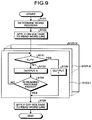
- FIG. 9 is a diagram illustrating a flow of processing by the control unit at the time of reading.
- FIG. 11 is a diagram illustrating a cross-section taken along a line A-A′ of elements according to the first example
- FIG. 12 is a diagram illustrating a cross-section taken along a line B-B′ of the elements according to the first example
- FIG. 14 is a diagram illustrating an arrangement of wires according to a second configuration example as viewed from a z-direction
- FIG. 15 is a diagram illustrating a cross-section taken along a line D-D′ of elements according to the second example
- FIG. 17 is a diagram illustrating timings of voltage application when a cell is charged.
- FIG. 18 is a diagram illustrating timings of voltage application when a cell is discharged.
- a semiconductor device includes M (M is an integer of 1 or more) write word lines including a first write word line to an M-th write word line, M read word lines including a first read word line to an M-th read word line, N (N is an integer of 1 or more) write bit lines including a first write bit line to an N-th write bit line, N read bit lines including a first read bit line to an N-th read bit line, N source lines including a first source line to an N-th source line, and M ⁇ N cells.
- the M ⁇ N cells are arranged in a matrix including M rows ⁇ N columns.
- a cell in an m-th (m is an integer of 1 to M) row ⁇ an n-th (n is an integer of 1 to N) column includes a first field effect transistor, a second field effect transistor, and a capacitor.
- the first field effect transistor is connected to an m-th write word line at a gate, to an n-th write bit line at a drain, and to a source of the second field effect transistor at a source.
- the second field effect transistor is connected to an m-th read word line at a gate and to an n-th read bit line at a drain.
- the capacitor is connected to an n-th source line at one end and to the source of the first field effect transistor at the other end.
- the arithmetic device 10 uses a plurality of capacitor type cells and performs a nonlinear operation that simulates neurons.
- the arithmetic device 10 realizes such a nonlinear operation with a very compact configuration.
- FIG. 1 is a diagram illustrating arithmetic processing by the arithmetic device 10 according to the embodiment.
- the arithmetic device 10 performs a plurality of nonlinear operations simultaneously.
- the arithmetic device 10 performs the nonlinear operation illustrated in FIG. 1 . That is, the arithmetic device 10 stores therein a plurality of weights w 1 to w i (i is an integer of 2 or more) set in advance.
- the arithmetic device 10 receives a plurality of pieces of input data x 1 to x i and multiplies the pieces of input data x 1 to x i by the corresponding weights w 1 to w i , respectively.
- the arithmetic device 10 adds all pieces of input data w 1 x 1 to w i x i respectively multiplied by the weights. That is, the arithmetic device 10 performs a product-sum operation for the pieces of input data x 1 to x i and the weights w 1 to w i .
- the arithmetic device 10 compares a result of the product-sum operation with a threshold value ⁇ set in advance.
- the arithmetic device 10 outputs 1 as output data y when the result of the product-sum operation is larger than the threshold value ⁇ , and outputs 0 when the result of the product-sum operation is equal to or smaller than the threshold value ⁇ .
- This arithmetic device 10 can, for example, perform an operation for one layer in a neural network by performing a set of nonlinear operations. Further, the arithmetic device 10 may repeat the set of nonlinear operations while changing weights. In this manner, the arithmetic device 10 can also perform operations for a plurality of layers in a multilayered neural network.
- FIG. 2 is a diagram illustrating a block configuration of the arithmetic device 10 .
- the arithmetic device 10 includes an arithmetic 12 and a control unit 14 .
- the arithmetic unit 12 includes a plurality of capacitor type cells and performs a plurality of nonlinear operations simultaneously.
- the control unit 14 receives weights and input data elements.
- the control unit 14 controls the arithmetic unit 12 in accordance with the received weights and pieces of input data.
- the control unit 14 outputs a result of operations by the arithmetic unit 12 as output data.
- the control unit 14 may supply the output data to another device, and the control unit 14 may feed back the output data to the control unit itself as input data.
- FIG. 3 is a diagram illustrating a configuration of the arithmetic unit 12 .
- the arithmetic unit 12 includes M (M is an integer of 1 or more) write word lines 21 , M read word lines 22 , N (N is an integer of 1 or more) write bit lines 23 , N read bit lines 24 , N source lines 25 , M ⁇ N cells 30 , and N comparators 32 .
- the arithmetic unit 12 includes a first write word line 21 - 1 to an M-th write word line 21 -M as the M write word lines 21 .
- Each of the M write word lines 21 is a wire formed in a semiconductor device, and a voltage is applied thereto by the control unit 14 .
- the M write word lines 21 are arranged in parallel to a first direction.
- the arithmetic unit 12 includes a first read word line 22 - 1 to an M-th read word line 22 -M as the M read word lines 22 .
- Each of the M read word lines 22 is a wire formed in a semiconductor device, and a voltage is applied thereto by the control unit 14 .
- the M read word lines 22 are arranged in parallel to the first direction.
- the arithmetic unit 12 includes a first write bit line 23 - 1 to an N-th write bit line 23 -N as the N write bit lines 23 .
- Each of the N write bit lines 23 is a wire formed in a semiconductor device, and a voltage is applied thereto by the control unit 14 .
- the N write bit lines 23 are arranged in parallel to a second direction that is perpendicular to the first direction.
- the arithmetic unit 12 includes a first read bit line 24 - 1 to an N-th read bit line 24 -N as the N read bit lines 24 .
- Each of the N read bit lines 24 is a wire formed in a semiconductor device.
- the N read bit lines 24 are arranged in parallel to the second direction.
- the arithmetic unit 12 includes a first source line 25 - 1 to an N-th source line 25 -N as the N source lines 25 .
- Each of the N source lines 25 is a wire formed in a semiconductor device, and a voltage is applied thereto by the control unit 14 .
- the N source lines 25 are arranged in parallel to the second direction.
- the M write word lines 21 and the M read word lines 22 are alternately arranged in the second direction in a semiconductor device.
- the N write bit lines 23 , the N read bit lines 24 , and the N source lines 25 are arranged one by one in sequence in the first direction in a semiconductor device.
- the M ⁇ N cells 30 are arranged in a matrix including M rows ⁇ N columns. Each of the M ⁇ N cells 30 is formed in a semiconductor device. Each of the M ⁇ N cells 30 is the same circuit.
- a cell 30 -( m ⁇ n ) in an m-th (m is any integer from 1 to M) row ⁇ an n-th (n is any integer from 1 to N) column is arranged in the vicinity of an m-th write word line 21 - m , an m-th read word line 22 - m , an n-th write bit line 23 - n , an n-th read bit line 24 - n , and an n-th source line 25 - n.
- the N comparators 32 are provided to respectively correspond to the N read bit lines 24 .
- the arithmetic unit 12 includes a first comparator 32 - 1 to an N-th comparator 32 -N as the N comparators 32 .
- Each of the N comparators 32 is connected to a corresponding read bit line 24 .
- Each of the N comparators 32 compares whether the voltage of the corresponding read bit line 24 is higher than a threshold voltage V th set in advance.
- an n-th comparator 32 - n is connected to the n-th read bit line 24 - n , and compares whether the voltage of the n-th read bit line 24 - n is higher than the threshold voltage V th .
- the threshold voltage V th may be settable for each comparator 32 , and may be different for each comparator 32 .
- each of the N comparators 32 outputs a pulse with a predetermined duration at a timing when the voltage of the corresponding read bit line 24 exceeds the threshold voltage V th .
- Each of the N comparators 32 may output 1 when the voltage of the corresponding read bit line 24 is higher than the threshold voltage V th , and may output 0 when the voltage of the corresponding read bit line 24 is equal to or lower than the threshold voltage V th .
- Each of the N comparators 32 provides a comparison result to the control unit 14 .
- FIG. 4 is a diagram illustrating a configuration of the cell 30 -( m ⁇ n ) in the m-th row ⁇ the n-th column.
- Each of the M ⁇ N cells 30 includes a first field effect transistor (first FET 41 ), a second field effect transistor (second FET 42 ), and a capacitor 43 .
- the first FET 41 and the second FET 42 are field effect transistors each having a channel formed of an oxide semiconductor. Therefore, a leak current in an off-state is very small in the first FET 41 and the second FET 42 .
- the first FET 41 of the cell 30 -( m ⁇ n ) in the m-th row ⁇ the n-th column is connected to the m-th write word line at a gate, to the n-th write bit line 23 - n at a drain, and to a source of the second FET 42 at a source.
- the second FET 42 of the cell 30 -( m ⁇ n ) in the m-th row ⁇ the n-th column is connected to the m-th read word line 22 - m at a gate, to the n-th read bit line 24 - n at a drain, and the source of the first FET 41 at a source.
- the capacitor 43 of the cell 30 -( m ⁇ n ) the m-th row ⁇ the n-th column is connected to the n-th source line 25 - n at one end and to a source of the first FET 41 and the source of the second FET 42 at the other end.
- the part between the source and the drain becomes conductive when an on-voltage (a voltage that turns on the first FET 41 ) is applied to the m-th write word line 21 - m . Further, in the first FET 41 of the cell 30 -( m ⁇ n ) in the m-th row ⁇ the n-th column, the part between the source and the drain becomes non-conductive when an off-voltage (a voltage that turns off the first FET 41 ) is applied to the m-th write word line 21 - m.
- the capacitor 43 When the first FET 41 of the cell 30 -( m ⁇ n ) in the m-th row ⁇ the n-th column is turned on, the capacitor 43 is charged or discharged in accordance with a potential difference between the n-th write bit line 23 - n and the n-th source line 25 - n .
- the capacitor 43 of the cell 30 -( m ⁇ n ) in the m-th row ⁇ the n-th column is charged.
- the capacitor 43 of the cell 30 -( m ⁇ n ) in the m-th row ⁇ the n-th column is discharged.
- the amount of charges that are charged to or discharged from the capacitor 43 of the cell 30 -( m ⁇ n ) in the m-th row ⁇ the n-th column is changed by the magnitude and the duration of the voltage applied to the n-th source line 25 - n.
- the control unit 14 applies an on-voltage to the m-th write word line 21 - m to respectively turn on the first FETs 41 of cells 30 -( m ⁇ 1) to 30 -( m ⁇ N) in the m-th row. Further, the control unit 14 applies an off-voltage to the write word lines 21 other than the m-th write word line 21 - m to respectively turn off the first FETs 41 of the cells 30 other than the cells 30 -( m ⁇ 1) to 30 -( m ⁇ n ) in the m-th row.
- the control unit 14 then applies a pulse with a voltage and a duration that correspond to the input data element to the n-th write bit line 23 - n . In this manner, the control unit 14 can write the charges corresponding to the input data element to the capacitor 43 of the cell 30 -( m ⁇ n ) in the m-th row ⁇ the n-th column.
- Writing charges to the capacitor 43 includes both a case of charging the capacitor 43 and a case of discharging the capacitor 43 .
- the control unit 14 may open the write bit lines 23 other than the n-th write bit line 23 - n (make them have a high impedance), in a case of applying the pulse with the voltage and the duration that correspond to the input data element to the n-th write bit line 23 - n.
- the capacitor 43 generates a voltage corresponding to charges accumulated therein. Therefore, the capacitor 43 generates a voltage corresponding to an input data element. Further, the first FET 41 has a small off leak current. Therefore, while the first FET 41 is off, the capacitor 43 continues to keep the charges and does not lower the voltage.
- the capacitor 43 can further accumulate charges while adding them to the currently accumulated charges.
- the control unit 14 writes charges corresponding to an input data element to the capacitor 43 for multiple times, it is possible to cause the capacitor 43 to generate a voltage corresponding to a value obtained by accumulatively adding a plurality of input data elements.
- the part between the source and the drain becomes conductive when an on-voltage (a voltage that turns on the second FET 42 ) is applied to the m-th read word line 22 - m . Further, in the second FET 42 of the cell 30 -( m ⁇ n ) in the m-th row ⁇ the n-th column, the part between the source and the drain becomes non-conductive when an off-voltage (a voltage that turns off the second FET 42 ) is applied to the m-th read word line 22 - m.
- the second FET 42 of the cell 30 -( m ⁇ n ) in the m-th row ⁇ the n-th column is turned on, the voltage generated by the capacitor 43 is applied to the n-th read bit line 24 - n .
- the n-th comparator 32 - n connected to the n-th read bit line 24 - n can compare the threshold voltage V th and the voltage generated by the capacitor 43 of the cell 30 -( m ⁇ n ) in the m-th row ⁇ the n-th column.
- the control unit 14 applies an on-voltage to the m-th read word line 22 - m to respectively turn on the second FETs 42 of the cells 30 -( m ⁇ 1) to 30 -( m ⁇ N) in the m-th row. Further, the control unit 14 applies an off-voltage to the read word lines 22 other than the m-th read word line 22 - m to respectively turn off the second FETs 42 of the cells 30 other than the cells 30 -( m ⁇ 1) to 30 -( m ⁇ N) in the m-th row.
- the control unit 14 then acquires a comparison result from the n-th comparator 32 - n of the N comparators 32 . In this manner, the control unit 14 can read the charges corresponding to the data written in the capacitor 43 of the cell 30 -( m ⁇ n ) In the m-th row ⁇ the n-th column.
- FIG. 5 is a diagram illustrating an example of voltage changes in the arithmetic unit 12 in a case of writing charges to the cell 30 -( m ⁇ n ) in the m-th row ⁇ the n-th column and a case of reading data corresponding to charges accumulated in the cell 30 -( m ⁇ n ) in the m-th row ⁇ the n-th column.
- the control unit 14 applies a pulse to the m-th write word line 21 - m .
- V WH is an on-voltage of the first FET 41 and the second FET 42 .
- V WL is an off-voltage of the first FET 41 and the second FET 42 .
- the control unit 14 applies a pulse to the n-th write bit line 23 - n , which is synchronized with the pulse applied to the m-th write word line 21 - m .
- a voltage of the pulse applied to the n-th write bit line 23 - n is V BH .
- V BH is a voltage corresponding to a value obtained by multiplying an input data element by a weight.
- the control unit 14 opens the write bit lines 23 other than the n-th write bit line 23 - n (makes them have a high impedance).
- the capacitor 43 of the cell 30 -( m ⁇ n ) in the m-th row the n-th column is charged when the pulses illustrated in (A) and (B) in FIG. 5 are applied. Therefore, as illustrated in (C) in FIG. 5 , the capacitor 43 of the cell 30 -( m ⁇ n ) in the m-th row ⁇ the n-th column generates a voltage corresponding to an integrated value of the applied pulses.
- the control unit 14 applies an on-voltage to the m-th read word line 22 - m .
- the timing of application of the on-voltage to the m-th read word line 22 - m may be asynchronous with the pulse applied to the m-th write word line 21 - m.
- the voltage of the capacitor 43 of the cell 30 -( m ⁇ n ) in the m-th row ⁇ the n-th column is generated in a period in which an on-voltage is applied to the m-th read word line 22 - m .
- the n-th comparator 32 - n generates a pulse at a timing (t 1 ) at which the voltage of the m-th read word line 22 - m exceeds the threshold voltage V th , as illustrated in (F) in FIG. 5 .
- FIG. 6 is a diagram illustrating an example of voltage changes of the write word line 21 and the write bit lines 23 at the time of writing.
- the control unit 14 selects a cell 30 for which writing is performed in a one-by-one manner.
- the control unit 14 applies a pulse to a write word line 21 corresponding to the selected cell 30 .
- the control unit 14 also applies a pulse with a voltage corresponding to a value obtained by multiplying an input data element by a weight to a corresponding write bit line 23 in synchronization with the pulse applied to the write word line 21 . In this manner, the control unit 14 can charge the selected cell 30 in accordance with the value obtained by multiplying the input data element by the weight.
- the control unit 14 then selects a next cell 30 and performs an identical process. Accordingly, the control unit 14 can write charges to the cells 30 in sequence.
- the control unit 14 may apply a pulse with a duration corresponding to the value obtained by multiplying an input data element by a weight to each of the corresponding write word line 21 and the corresponding write bit line 23 .
- the control unit 14 When applying a pulse to one write word line 21 , the control unit 14 applies an off-voltage to the other write word lines 21 . Further, when applying a pulse to the write bit line 23 to which the cell 30 for which writing is performed is connected, the control unit 14 opens the other write bit line 23 (makes it have a high impedance). In this manner, the control unit 14 can eliminate erroneous writing of charges to cells 30 other than the selected cell 30 .
- control unit 14 may simultaneously select a plurality of cells 30 connected to the same write word line 21 as cells 30 for which writing is performed. In this case, the control unit 14 applies a pulse to each of a plurality of write bit lines 23 to which the selected cells 30 are respectively connected.
- FIG. 7 is a diagram illustrating an example of voltage changes of the read word line 22 and the read bit lines 24 at the time of reading.
- the control unit 14 selects a cell 30 for which reading is performed and specifies a read word line 22 including the selected cell 30 .
- the control unit 14 applies an on-voltage to the specified read word line 22 .
- the control unit 14 can read data corresponding to charges accumulated in each of a plurality of cells 30 connected to the specified read word line 22 .
- control unit 14 When applying an on-voltage to one read word line 22 , the control unit 14 applies an off-voltage to the other read word lines 22 . In this manner, the control unit 14 can eliminate erroneous writing of charges from the cell 30 connected to the specified read word line 22 to a cell 30 connected to the other read word line 22 .
- FIG. 8 is a diagram illustrating a flow of processing by the control unit 14 at the time of writing.
- the control unit 14 performs the processing illustrated in FIG. 8 at the time of writing.
- the control unit 14 acquires an input data element. Subsequently, at S 112 , the control unit 14 then specifies a word address and a bit address of a cell 30 to which writing is performed. Thereafter, at S 113 , the control unit 14 acquires a weight by which the input data is multiplied.
- the control unit 14 determines a pulse voltage to be applied to each of a corresponding write word line 21 and a corresponding write bit line 23 .
- the control unit 14 determines a pulse voltage corresponding to a value that is a result of multiplication of the acquired weight and the input data element.
- the control unit 14 may determine a duration of a pulse to be applied to each of the corresponding write word line 21 and the corresponding write bit line 23 .
- control unit 14 applies a pulse with a determined voltage to a write word line 21 at the specified word address and a write bit line 23 at the specified bit address. After ending the process at S 115 , the control unit 14 ends the processing in this flow. In this manner, the control unit 14 can write charges corresponding to an input data element to a corresponding cell 30 .
- FIG. 9 is a diagram illustrating a flow of processing by the control unit 14 at the time of reading.
- the control unit 14 performs the processing illustrated in FIG. 9 at the time of reading.
- the control unit 14 determines a word address of a cell 30 for which reading is performed. Subsequently, at S 122 , the control unit 14 applies an on-voltage to a read word line 22 at the determined word address.
- control unit 14 performs a process at S 123 (S 123 - 1 to S 123 -N) for each of a plurality of bit addresses simultaneously.
- control unit 14 performs processes at S 131 to S 134 .
- the control unit 14 determines whether a voltage V 1 of a corresponding read bit line 24 is larger than the threshold voltage V th . Specifically, the control unit 14 determines whether a pulse has been output from a corresponding comparator 32 . In a case where the voltage V 1 of the corresponding read bit line 24 is larger than the threshold voltage V th (YES at S 131 ), the control unit 14 outputs 1 as output data at S 132 . After ending the process at S 132 , the control unit 14 ends the process at S 123 and advances the process to S 124 .
- the control unit 14 In a case where the voltage V 1 of the corresponding read bit line 24 is not larger than the threshold voltage V th (NO at S 131 ), the control unit 14 outputs 0 as output data at S 133 . Subsequent to S 133 , at S 134 , the control unit 14 determines whether to end a reading process. When the reading process is not ended (NO at S 134 ), the control unit 14 returns the process to S 131 . When the reading process is ended (YES at S 134 ), the control unit 14 ends the process at S 123 and advances the process to S 124 .
- control unit 14 applies an off-voltage to the read word line 22 at the determined word address. After ending the process at S 124 , the control unit 14 ends the processing in this flow. In this manner, the control unit 14 can read data corresponding to charges accumulated in the cell 30 .
- FIG. 10 is a diagram illustrating an arrangement of wires in the vicinity of the cell 30 -( m ⁇ n ) in the m-th row ⁇ the n-th column according to the first configuration example as viewed from a z-direction.
- the vertical direction (the direction in which films are stacked) is the z-direction (a third direction)
- an arbitrary direction in a horizontal plane parallel to the films is an x-direction (the first direction)
- a direction perpendicular to the x-direction in the plane parallel to the films is a y-direction (the second direction).
- the m-th write word line 21 - m and the m-th read word line 22 - m are formed of a conductive material such as metal.
- the m-th write word line 21 - m and the m-th read word line 22 - m are formed to be parallel to the x-direction.
- the m-th write word line 21 - m and the m-th read word line 22 - m are formed at positions overlapping each other as viewed from the a-direction (in an x-y plane).
- the n-th write bit line 23 - n and the n-th read bit line 24 - n are formed of a conductive material such as metal.
- the n-th write bit line 23 - n and the n-th read bit line 24 - n are formed to be parallel to the y-direction.
- the n-th write bit line 23 - n and the n-th read bit line 24 - n are formed at positions overlapping each other as viewed from the z-direction (in the x-y plane).
- the n-th source line 25 - n is formed of a conductive material such as metal.
- the n-th source line 25 - n is formed to be parallel to the y-direction.
- the n-th source line 25 - n is formed in a region different from the n-th write bit line 23 - n and the n-th read bit line 24 - n as viewed from the direction (in the x-y plane).
- FIGS. 11 and 12 are diagrams respectively illustrating an arrangement of elements in the vicinity of the cell 30 -( m ⁇ n ) in the m-th row ⁇ the n-th column according to the first configuration example as viewed from the x-direction.
- the hatched element in FIG. 11 represents a cross-section taken along a line A-A′ in FIG. 10 .
- the hatched element in FIG. 12 represents a cross-section taken along a line B-B′ in FIG. 10 .
- the m-th write word line 21 - m and the m-th read word line 22 - m are formed in different layers from each other in the z-direction.
- the n-th write bit line 23 - n and the n-th read bit line 24 - n are formed in different layers from each other in the z-direction.
- the m-th write word line 21 - m and the m-th read word line 22 - m are formed in a region between the n-th write bit line 23 - n and the n-th read bit line 24 - n in the z-direction.
- the m-th write word line 21 - m is formed on a side close to the n-th write bit line 23 - n
- the m-th read word line 22 - m is formed on a side close to the n-th read bit line 24 - n .
- the n-th source line 25 - n is formed in a region between the m-th write word line 21 - m and the m-th read word line 22 - m in the z-direction.
- the first FET 41 of the cell 30 -( m ⁇ n ) in the m-th row the n-th column is formed in a region where the m-th write word line 21 - m and the n-th write bit line 23 - n overlap each other as viewed from the z-direction (in the x-y plane).
- the second FET 42 of the cell 30 -( m ⁇ n ) in the m-th row ⁇ the n-th column is formed in a region where the m-th read word line 22 - m and the n-th read bit line 24 - n overlap each other as viewed from the z-direction (in the x-y plane).
- Each of the first FET 41 and the second FET 42 includes a channel 61 and a gate insulating film 62 .
- the m-th write word line 21 - m functions a gate electrode.
- the m-th read word line 22 - m functions as a gate electrode.
- a source and a drain are arranged in the direction. That is, in the first FET 41 and the second FET 42 , a direction in which charges are caused to flow by the channel 61 is formed along the z-direction (the direction perpendicular to the x-direction (the first direction) and the y-direction (the second direction)).
- the channel 61 of the first FET 41 is formed inside through hole extending through the m-th write word line 21 - m in the z-direction.
- the gate insulating film 62 is formed between the channel 61 of the first FET 41 and the m-th write word line 21 - m.
- the channel 61 of the second FET 42 is formed inside a through hole extending through the m-th read word line 22 - m in the z-direction. Further, the gate insulating film 62 is formed between the channel 61 of the second FET 42 and the m-th read word line 22 - m.
- the drain of the first FET 41 is connected to the n-th write bit line 23 - n .
- the drain of the second FET 42 is connected to the n-th read bit line 24 - n .
- the source of the first FET 41 and the source of the second FET 42 are connected to an interlayer wire 63 .
- the capacitor 43 of the cell 30 -( m ⁇ n ) in the m-th row the n-th column includes a trench wall 64 and an electrode portion 65 .
- the trench wall 64 is formed of a conductive material.
- the trench wall 64 is hollow and tubular.
- the trench wall 64 is connected to the interlayer wire 63 .
- the electrode portion 65 is in a shape of a bar inserted into the trench wall 64 and is formed of a conductive material. A dielectric material may be included between the trench wall 64 and the electrode portion 65 .
- the electrode portion 65 is connected the n-th source line 25 - n.
- the capacitor 43 described above is formed between the m-th write word line 21 - m and the m-th read word line m in the a-direction. Therefore, the capacitor 43 is formed at a position that does not interfere with any of the M write word lines 21 , the M read word lines 22 , the N write bit lines 23 , and the N read bit lines 24 in the z-direction.
- FIG. 13 is a diagram illustrating an arrangement of elements in the vicinity of the cell 30 -( m ⁇ n ) in the m-th row the n-th column according to the first configuration example as viewed from the z-direction.
- the hatched element in FIG. 13 represents a cross-section taken along a line C-C′ in FIGS. 11 and 12 .
- the capacitor 43 is formed at a position that does not overlap the m-th write word line 21 - m and the n-th write bit line 23 - n as viewed from the z-direction (in the x-y plane). Therefore, the capacitor 43 is formed at a position that does not interfere with any of the M write word lines 21 , the M read word lines 22 , the N write bit lines 23 , and the N read bit lines 24 in the x-direction and the y-direction.
- the arithmetic device 10 can be implemented by a semiconductor device.
- the channels 61 of the first FET 41 and the second FET 42 are formed of an oxide semiconductor.
- the channel 61 can be formed of, for example, an oxide semiconductor containing indium (In), gallium (Ga), and zinc (Zn), which is so-called IGZO.
- the channel 61 can be formed of a metal oxide semiconductor such as InGaZnO, InSnZnO, InZnO, InGaSnZnO, In 2 O 3 , Ga 2 O 3 , or ZnO.
- a second configuration example of the arithmetic device 10 is described in a case where it is implemented by a semiconductor device.
- the relation among the x-direction (the first direction), the y-direction (the second direction), and the z-direction (the third direction) is identical to that in the first configuration example. Further, constituent elements substantially identical to those in the first configuration example are denoted by like reference characters and detailed descriptions thereof are omitted.
- FIG. 14 is a diagram illustrating an arrangement of wires in the vicinity of the cell 30 -( m ⁇ n ) in the m-th row ⁇ the n-th column according to the second configuration example as viewed from the z-direction.
- the m-th write word line 21 - m and the m-th read word line 22 - m are formed to be parallel to the x-direction.
- the m-th write word line 21 - m and the m-th read word line 22 - m are formed in the same layer (in the same x-y plane) as each other.
- the n-th write bit line 23 - n and the n-th read bit line 24 - n are formed to be parallel to the y-direction.
- the n-th write bit line 23 - n and the n-th read bit line 24 - n are formed in the same layer (in the same x-y plane) as each other.
- the m-th write word line 21 - m and the m-th read word line 22 - m are formed below the n-th write bit line 23 - n and the n-th read bit line 24 - n.
- FIG. 15 is a diagram illustrating an arrangement of elements in the vicinity of the cell 30 -( m ⁇ n ) in the m-th row ⁇ the n-th column according to the second configuration example as viewed from the x-direction.
- the hatched element in FIG. 15 represents a cross-section taken along a line D-D′ in FIG. 14 .
- the n-th source line 25 - n is formed to be parallel to the y-direction.
- the n-th source line 25 - n is formed below the m-th write word line 21 - m and the m-th read word line 22 - m.
- An oxide semiconductor layer 66 is formed below the m-th write word line 21 - m and the m-th read word line 22 - m .
- the channel 61 of the first FET 41 is formed in the oxide semiconductor layer 66 below the m-th write word line 21 - m .
- the channel 61 of the second FET 42 is formed in the oxide semiconductor layer 66 below the m-th read word line 22 - m.
- a source and a drain are arranged in the y-direction. That is, in the first FET 41 and the second FET 42 , the direction in which charges are caused to flow by the channel 61 is formed along the y-direction (the second direction).
- the gate insulating film 62 is formed between the channel 61 of the first FET 41 and the m-th write word line 21 - m .
- the gate insulating film 62 is formed between the channel 61 of the second FET 42 and the m-th read word line 22 - m .
- the source of the first FET 41 and the source of the second FET 42 are connected to each other via the oxide semiconductor layer 66 .
- the drain of the first FET 41 is connected to the n-th write bit line 23 - n via a first interlayer wire 67 .
- the drain of the second FET 42 is connected to the n-th read bit line 24 - n via a second interlayer wire 68 .
- the capacitor 43 of the cell 30 -(in the m-th row ⁇ the n-th column has the trench wall 64 and the electrode portion 65 .
- the trench wall 64 is connected to the n-th source line 25 - n .
- the electrode portion 65 is connected to the source of the first FET 41 and the source of the second FET 42 .
- the arithmetic device 10 can be implemented by a semiconductor device including a planar transistor.
- the arithmetic device 10 of the present embodiment it is possible to downscale the configuration of the control unit 14 and to reduce various types of wires by arranging the capacitor-type cells 30 in a matrix. Further, the arithmetic device 10 according to the present embodiment includes the second FET 42 that is turned on at the time of reading of a cell 30 , and therefore it is possible to prevent charges from being accidentally written to another cell 30 at the time of reading data.
- FIG. 16 is a diagram illustrating an example of voltage changes in the arithmetic device 10 according to a first modification.
- the control unit 14 according to the first modification controls a voltage relation between a write bit line 23 and a source line 25 at the time of writing of charges to the cells 30 .
- the control unit 14 sets the voltage of the n-th write bit line 23 - n with respect to the n-th source line 25 - n as a first voltage that is higher than the voltage of the capacitor 43 of the cell 30 -( m ⁇ n ) in the m-th row ⁇ the n-th column.
- the control unit 14 sets the voltage of the n-th write bit line 23 - n with respect to the n-th source line 25 - n as a second voltage that is equal to or lower than 0 (zero).
- the control unit 14 applies pulses to the n-th write bit line 23 - n and the m-th write word line 21 - m , which are synchronized with each other, as indicated at times t 11 , t 12 , and t 14 in FIG. 16 .
- the control unit 14 applies a reference voltage V SL for example, a ground voltage or a common voltage) to the n-th source line 25 - n.
- the control unit 14 applies pulses to the n-th source line 25 and the m-th write word line 21 - m , which are synchronized with each other, as indicated at a time t 13 in FIG. 16 .
- the control unit 14 applies a reference voltage V BL (for example, a ground voltage or a common voltage) to the n-th write bit line 23 - n .
- V BL for example, a ground voltage or a common voltage
- a pulse voltage V SH applied to the n-th source line 25 - n is equal to or higher than the reference voltage V BL applied to the n-th write bit line 23 - n.
- control unit 14 can charge the cell 30 to raise the voltage of the capacitor 43 of the cell 30 or can discharge the cell 30 to lower the voltage of the capacitor 43 .
- the control unit 14 may change the voltage to be applied to the source line 25 asynchronously with a pulse applied to the write bit line 23 .
- the control unit 14 may switch the voltage applied to the source line 25 at random.
- FIG. 17 is a diagram illustrating an example of timings of voltage application to the write word line 21 and the write bit line 23 when the cell 30 is charged in the arithmetic device 10 according to a second modification.
- the control unit 14 according to the second modification controls a phase relation between a pulse applied to the write word line 21 and a pulse applied to the write bit line 23 at the time of writing charges to the cell 30 .
- the control unit 14 applies a pulse to the n-th write bit line 23 - n at a timing that a first period in which a first voltage is applied to the n-th write bit line 23 - n is longer than a second period in which a second voltage is applied to the n-th write bit line 23 - n in an on-period in which an on-voltage is applied to the m-th write word line 21 - m .
- charges are accumulated in the capacitor 43 of the cell 30 -( m ⁇ n ) the m-th row ⁇ the n-th column.
- the capacitor 43 of the cell 30 -( m ⁇ n ) in the m-th row ⁇ the n-th column is discharged. Therefore, in a case where the first period is longer than the second period, the capacitor 43 of the cell 30 -( m ⁇ n ) in the m-th row ⁇ the n-th column is charged eventually.
- a central time of a pulse applied to the m-th write word line 21 - m is t m
- a time of an end edge of a pulse applied to the n-th write bit line 23 - n is t e .
- the control unit 14 applies the pulse to the n-th write bit line 23 - n at a timing when ⁇ t exceeds 0.
- the duration of the pulse applied to the n-th write bit line 23 - n is at least 1 ⁇ 2 of the pulse applied to the m-th write word line 21 - m.
- FIG. 18 is a diagram illustrating an example of timings of voltage application to the write word line 21 and the write bit line 23 when the cell 30 is discharged in the arithmetic device 10 according to the second modification.
- the control unit 14 applies a pulse to the n-th write bit line 23 - n at a timing that the first period in which the first voltage is applied to the n-th write bit line 23 - n is shorter than the second period in which the second voltage is applied to the n-th write bit line 23 - n in the on-period in which an on-voltage is applied to the m-th write word line 21 - m .
- charges are accumulated in the capacitor 43 of the cell 30 -( m ⁇ n ) in the m-th row ⁇ the n-th column.
- the capacitor 43 of the cell 30 -( m ⁇ n ) in the m-th row ⁇ the n-th column is discharged. Therefore, in a case where the first period is shorter than the second period, the capacitor 43 of the cell 30 -( m ⁇ n ) in the m-th row ⁇ the n-th column is discharged eventually.
- the control unit 14 applies the pulse to the n-th write bit line 23 - n at a timing that ⁇ t falls below 0.
- control unit 14 can charge the cell 30 to raise the voltage of the capacitor 43 of the cell 30 or can discharge the cell 30 to lower the voltage of the capacitor 43 .
- control unit 14 may change the phase relation between the pulse applied to the write word line 21 and the pulse applied to the write bit line 23 in accordance with a corresponding status.
- control unit 14 may switch the phase relation illustrated in FIG. 1 phase relation in charging) and the phase relation illustrated in FIG. 18 (a phase relation in discharging) to each other in accordance with a corresponding status.
- control unit 14 may set the phase relation in charging at initial setting, and may switch it to the phase relation in discharging in accordance with a timing when predetermined data (for example, 1) is read from the cell 30 -( m ⁇ n ) in the m-th row ⁇ the n-th column.
- predetermined data for example, 1
- the control unit 14 may switch whether to set the phase relation in charging or the phase relation in discharging in accordance with a time from the start of writing of charges to the cell 30 -( m ⁇ n ) in the m-th row ⁇ the n-th column to a time at which accumulated charges in the cell 30 -( m ⁇ n ) in the m-th row ⁇ the n-th column reach a predetermined threshold value.
- the arithmetic device it according to the second modification can easily realize control referred to as “STDP (Spike-timing dependent synaptic plasticity)” in a neuromorphic device.
- STDP spike-timing dependent synaptic plasticity
- the arithmetic device 10 according to the second modification is only required to control the phases of pulses respectively applied to the write word line 21 and the write bit line 23 . Therefore, it is possible to realize STOP with a small circuit without providing a complicated circuit for generating a waveform.
Landscapes
- Engineering & Computer Science (AREA)
- Computer Hardware Design (AREA)
- Microelectronics & Electronic Packaging (AREA)
- Physics & Mathematics (AREA)
- Theoretical Computer Science (AREA)
- Health & Medical Sciences (AREA)
- Life Sciences & Earth Sciences (AREA)
- Biomedical Technology (AREA)
- Biophysics (AREA)
- Software Systems (AREA)
- Neurology (AREA)
- Molecular Biology (AREA)
- General Health & Medical Sciences (AREA)
- Artificial Intelligence (AREA)
- Computing Systems (AREA)
- General Engineering & Computer Science (AREA)
- General Physics & Mathematics (AREA)
- Mathematical Physics (AREA)
- Evolutionary Computation (AREA)
- Data Mining & Analysis (AREA)
- Computational Linguistics (AREA)
- Databases & Information Systems (AREA)
- Computer Vision & Pattern Recognition (AREA)
- Medical Informatics (AREA)
- Semiconductor Memories (AREA)
- Dram (AREA)
- Read Only Memory (AREA)
Abstract
Description
Claims (19)
Applications Claiming Priority (2)
| Application Number | Priority Date | Filing Date | Title |
|---|---|---|---|
| JP2017141298A JP2019021367A (en) | 2017-07-20 | 2017-07-20 | Semiconductor device |
| JP2017-141298 | 2017-07-20 |
Publications (2)
| Publication Number | Publication Date |
|---|---|
| US20190026628A1 US20190026628A1 (en) | 2019-01-24 |
| US10621490B2 true US10621490B2 (en) | 2020-04-14 |
Family
ID=65023013
Family Applications (1)
| Application Number | Title | Priority Date | Filing Date |
|---|---|---|---|
| US15/899,390 Active 2038-03-03 US10621490B2 (en) | 2017-07-20 | 2018-02-20 | Semiconductor device |
Country Status (2)
| Country | Link |
|---|---|
| US (1) | US10621490B2 (en) |
| JP (1) | JP2019021367A (en) |
Families Citing this family (2)
| Publication number | Priority date | Publication date | Assignee | Title |
|---|---|---|---|---|
| US11322199B1 (en) * | 2020-10-09 | 2022-05-03 | Qualcomm Incorporated | Compute-in-memory (CIM) cell circuits employing capacitive storage circuits for reduced area and CIM bit cell array circuits |
| KR102565801B1 (en) * | 2021-06-17 | 2023-08-10 | 서강대학교산학협력단 | Neuromorphic computing system |
Citations (11)
| Publication number | Priority date | Publication date | Assignee | Title |
|---|---|---|---|---|
| JPS5858020B2 (en) | 1978-08-17 | 1983-12-23 | 日立造船株式会社 | Method for detecting cracks in bottle-shaped bodies |
| US5165009A (en) * | 1990-01-24 | 1992-11-17 | Hitachi, Ltd. | Neural network processing system using semiconductor memories |
| JP2000222876A (en) | 1999-01-29 | 2000-08-11 | Matsushita Electric Ind Co Ltd | Semiconductor storage device |
| US6151244A (en) * | 1998-03-17 | 2000-11-21 | Mitsubishi Denki Kabushiki Kaisha | Dynamic semiconductor memory device |
| JP2009080892A (en) | 2007-09-26 | 2009-04-16 | Toshiba Corp | Semiconductor memory device |
| US8837202B2 (en) | 2010-09-29 | 2014-09-16 | Semiconductor Energy Laboratory Co., Ltd. | Semiconductor memory device and method for driving the same |
| US20150100532A1 (en) | 2013-10-03 | 2015-04-09 | Denso Corporation | Group information storing and recognizing apparatus |
| US20150249096A1 (en) * | 2012-09-10 | 2015-09-03 | James John Lupino | Three dimension integrated circuits employing thin film transistors |
| US20160343452A1 (en) | 2015-05-21 | 2016-11-24 | Semiconductor Energy Laboratory Co., Ltd. | Electronic Device |
| US20160350647A1 (en) | 2015-05-26 | 2016-12-01 | International Business Machines Corporation | Neuron peripheral circuits for neuromorphic synaptic memory array based on neuron models |
| US20180277192A1 (en) | 2017-03-21 | 2018-09-27 | Toshiba Memory Corporation | Semiconductor memory device |
-
2017
- 2017-07-20 JP JP2017141298A patent/JP2019021367A/en active Pending
-
2018
- 2018-02-20 US US15/899,390 patent/US10621490B2/en active Active
Patent Citations (17)
| Publication number | Priority date | Publication date | Assignee | Title |
|---|---|---|---|---|
| JPS5858020B2 (en) | 1978-08-17 | 1983-12-23 | 日立造船株式会社 | Method for detecting cracks in bottle-shaped bodies |
| US5165009A (en) * | 1990-01-24 | 1992-11-17 | Hitachi, Ltd. | Neural network processing system using semiconductor memories |
| US6151244A (en) * | 1998-03-17 | 2000-11-21 | Mitsubishi Denki Kabushiki Kaisha | Dynamic semiconductor memory device |
| JP2000222876A (en) | 1999-01-29 | 2000-08-11 | Matsushita Electric Ind Co Ltd | Semiconductor storage device |
| US6181620B1 (en) | 1999-01-29 | 2001-01-30 | Matsushita Electric Industrial Co., Ltd. | Semiconductor storage device |
| JP2009080892A (en) | 2007-09-26 | 2009-04-16 | Toshiba Corp | Semiconductor memory device |
| US8001065B2 (en) | 2007-09-26 | 2011-08-16 | Kabushiki Kaisha Toshiba | Semiconductor storage device |
| JP5789465B2 (en) | 2010-09-29 | 2015-10-07 | 株式会社半導体エネルギー研究所 | Semiconductor memory device |
| US8837202B2 (en) | 2010-09-29 | 2014-09-16 | Semiconductor Energy Laboratory Co., Ltd. | Semiconductor memory device and method for driving the same |
| US20150249096A1 (en) * | 2012-09-10 | 2015-09-03 | James John Lupino | Three dimension integrated circuits employing thin film transistors |
| US20150100532A1 (en) | 2013-10-03 | 2015-04-09 | Denso Corporation | Group information storing and recognizing apparatus |
| JP5858020B2 (en) | 2013-10-03 | 2016-02-10 | 株式会社デンソー | Group information memory recognition device |
| US20160343452A1 (en) | 2015-05-21 | 2016-11-24 | Semiconductor Energy Laboratory Co., Ltd. | Electronic Device |
| JP2016219011A (en) | 2015-05-21 | 2016-12-22 | 株式会社半導体エネルギー研究所 | Electronic equipment |
| US20160350647A1 (en) | 2015-05-26 | 2016-12-01 | International Business Machines Corporation | Neuron peripheral circuits for neuromorphic synaptic memory array based on neuron models |
| US20180277192A1 (en) | 2017-03-21 | 2018-09-27 | Toshiba Memory Corporation | Semiconductor memory device |
| JP2018156575A (en) | 2017-03-21 | 2018-10-04 | 東芝メモリ株式会社 | Semiconductor memory device |
Also Published As
| Publication number | Publication date |
|---|---|
| US20190026628A1 (en) | 2019-01-24 |
| JP2019021367A (en) | 2019-02-07 |
Similar Documents
| Publication | Publication Date | Title |
|---|---|---|
| US10242737B1 (en) | Device structure for neuromorphic computing system | |
| US9431099B2 (en) | Neuromorphic device with excitatory and inhibitory functionalities | |
| US11170839B2 (en) | Programming non-volatile memory arrays with automatic programming pulse amplitude adjustment using current-limiting circuits | |
| US10103162B2 (en) | Vertical neuromorphic devices stacked structure and array of the structure | |
| TWI699711B (en) | Memory devices and manufacturing method thereof | |
| US20180012660A1 (en) | Memory device including multiple select gates and different bias conditions | |
| US9318200B2 (en) | Methods and apparatuses including a string of memory cells having a first select transistor coupled to a second select transistor | |
| CN111581141B (en) | Memory device and method of operating the same | |
| CN117157636A (en) | Integrated deposit and calculation device, system and operation method thereof | |
| US20200202941A1 (en) | Non-volatile memory cell compliant to a near-memory computation system | |
| US9263145B2 (en) | Current detection circuit and semiconductor memory apparatus | |
| US10593403B2 (en) | Memristive arrays with a waveform generation device | |
| US10621490B2 (en) | Semiconductor device | |
| US11455371B2 (en) | Computation circuit for performing vector-matrix multiplication and semiconductor device including the computation circuit | |
| EP4381502B1 (en) | Input circuitry for analog neural memory in a deep learning artificial neural network | |
| US20240404598A1 (en) | 3d cell and array structures | |
| Heittmann et al. | Limits of writing multivalued resistances in passive nanoelectronic crossbars used in neuromorphic circuits | |
| Kang et al. | Short-and long-term memory based on a floating-gate IGZO synaptic transistor | |
| US10354725B2 (en) | Method for rewriting semiconductor storage device and the semiconductor storage device | |
| TW201440055A (en) | Semiconductor devices and semiconductor systems including the same | |
| CN113380289B (en) | Memory circuit and method of writing into memory cells | |
| US10910054B2 (en) | Charge separation for memory sensing | |
| KR102820923B1 (en) | Artificial neural network system based on capacitive coupling | |
| Choi et al. | Highly-efficient and scalable TrioN (3N0C) synaptic cell for analog process-in-memory | |
| US9502122B2 (en) | Systems, devices and methods for memory operations |
Legal Events
| Date | Code | Title | Description |
|---|---|---|---|
| FEPP | Fee payment procedure |
Free format text: ENTITY STATUS SET TO UNDISCOUNTED (ORIGINAL EVENT CODE: BIG.); ENTITY STATUS OF PATENT OWNER: LARGE ENTITY |
|
| AS | Assignment |
Owner name: KABUSHIKI KAISHA TOSHIBA, JAPAN Free format text: ASSIGNMENT OF ASSIGNORS INTEREST;ASSIGNORS:TANAKA, CHIKA;IKEDA, KEIJI;REEL/FRAME:045482/0584 Effective date: 20180330 |
|
| STPP | Information on status: patent application and granting procedure in general |
Free format text: DOCKETED NEW CASE - READY FOR EXAMINATION |
|
| STPP | Information on status: patent application and granting procedure in general |
Free format text: NON FINAL ACTION MAILED |
|
| STPP | Information on status: patent application and granting procedure in general |
Free format text: RESPONSE TO NON-FINAL OFFICE ACTION ENTERED AND FORWARDED TO EXAMINER |
|
| STPP | Information on status: patent application and granting procedure in general |
Free format text: NOTICE OF ALLOWANCE MAILED -- APPLICATION RECEIVED IN OFFICE OF PUBLICATIONS |
|
| STCF | Information on status: patent grant |
Free format text: PATENTED CASE |
|
| MAFP | Maintenance fee payment |
Free format text: PAYMENT OF MAINTENANCE FEE, 4TH YEAR, LARGE ENTITY (ORIGINAL EVENT CODE: M1551); ENTITY STATUS OF PATENT OWNER: LARGE ENTITY Year of fee payment: 4 |