US10620537B2 - Resist underlayer film composition, patterning process, method for forming resist underlayer film, and compound for resist underlayer film composition - Google Patents
Resist underlayer film composition, patterning process, method for forming resist underlayer film, and compound for resist underlayer film composition Download PDFInfo
- Publication number
- US10620537B2 US10620537B2 US15/621,482 US201715621482A US10620537B2 US 10620537 B2 US10620537 B2 US 10620537B2 US 201715621482 A US201715621482 A US 201715621482A US 10620537 B2 US10620537 B2 US 10620537B2
- Authority
- US
- United States
- Prior art keywords
- general formula
- group
- underlayer film
- resist underlayer
- resist
- Prior art date
- Legal status (The legal status is an assumption and is not a legal conclusion. Google has not performed a legal analysis and makes no representation as to the accuracy of the status listed.)
- Active
Links
Images


Classifications
-
- G—PHYSICS
- G03—PHOTOGRAPHY; CINEMATOGRAPHY; ANALOGOUS TECHNIQUES USING WAVES OTHER THAN OPTICAL WAVES; ELECTROGRAPHY; HOLOGRAPHY
- G03F—PHOTOMECHANICAL PRODUCTION OF TEXTURED OR PATTERNED SURFACES, e.g. FOR PRINTING, FOR PROCESSING OF SEMICONDUCTOR DEVICES; MATERIALS THEREFOR; ORIGINALS THEREFOR; APPARATUS SPECIALLY ADAPTED THEREFOR
- G03F7/00—Photomechanical, e.g. photolithographic, production of textured or patterned surfaces, e.g. printing surfaces; Materials therefor, e.g. comprising photoresists; Apparatus specially adapted therefor
- G03F7/004—Photosensitive materials
- G03F7/039—Macromolecular compounds which are photodegradable, e.g. positive electron resists
- G03F7/0392—Macromolecular compounds which are photodegradable, e.g. positive electron resists the macromolecular compound being present in a chemically amplified positive photoresist composition
-
- G—PHYSICS
- G03—PHOTOGRAPHY; CINEMATOGRAPHY; ANALOGOUS TECHNIQUES USING WAVES OTHER THAN OPTICAL WAVES; ELECTROGRAPHY; HOLOGRAPHY
- G03F—PHOTOMECHANICAL PRODUCTION OF TEXTURED OR PATTERNED SURFACES, e.g. FOR PRINTING, FOR PROCESSING OF SEMICONDUCTOR DEVICES; MATERIALS THEREFOR; ORIGINALS THEREFOR; APPARATUS SPECIALLY ADAPTED THEREFOR
- G03F7/00—Photomechanical, e.g. photolithographic, production of textured or patterned surfaces, e.g. printing surfaces; Materials therefor, e.g. comprising photoresists; Apparatus specially adapted therefor
- G03F7/0002—Lithographic processes using patterning methods other than those involving the exposure to radiation, e.g. by stamping
-
- G—PHYSICS
- G03—PHOTOGRAPHY; CINEMATOGRAPHY; ANALOGOUS TECHNIQUES USING WAVES OTHER THAN OPTICAL WAVES; ELECTROGRAPHY; HOLOGRAPHY
- G03F—PHOTOMECHANICAL PRODUCTION OF TEXTURED OR PATTERNED SURFACES, e.g. FOR PRINTING, FOR PROCESSING OF SEMICONDUCTOR DEVICES; MATERIALS THEREFOR; ORIGINALS THEREFOR; APPARATUS SPECIALLY ADAPTED THEREFOR
- G03F7/00—Photomechanical, e.g. photolithographic, production of textured or patterned surfaces, e.g. printing surfaces; Materials therefor, e.g. comprising photoresists; Apparatus specially adapted therefor
- G03F7/004—Photosensitive materials
- G03F7/025—Non-macromolecular photopolymerisable compounds having carbon-to-carbon triple bonds, e.g. acetylenic compounds
-
- G—PHYSICS
- G03—PHOTOGRAPHY; CINEMATOGRAPHY; ANALOGOUS TECHNIQUES USING WAVES OTHER THAN OPTICAL WAVES; ELECTROGRAPHY; HOLOGRAPHY
- G03F—PHOTOMECHANICAL PRODUCTION OF TEXTURED OR PATTERNED SURFACES, e.g. FOR PRINTING, FOR PROCESSING OF SEMICONDUCTOR DEVICES; MATERIALS THEREFOR; ORIGINALS THEREFOR; APPARATUS SPECIALLY ADAPTED THEREFOR
- G03F7/00—Photomechanical, e.g. photolithographic, production of textured or patterned surfaces, e.g. printing surfaces; Materials therefor, e.g. comprising photoresists; Apparatus specially adapted therefor
- G03F7/004—Photosensitive materials
- G03F7/027—Non-macromolecular photopolymerisable compounds having carbon-to-carbon double bonds, e.g. ethylenic compounds
-
- G—PHYSICS
- G03—PHOTOGRAPHY; CINEMATOGRAPHY; ANALOGOUS TECHNIQUES USING WAVES OTHER THAN OPTICAL WAVES; ELECTROGRAPHY; HOLOGRAPHY
- G03F—PHOTOMECHANICAL PRODUCTION OF TEXTURED OR PATTERNED SURFACES, e.g. FOR PRINTING, FOR PROCESSING OF SEMICONDUCTOR DEVICES; MATERIALS THEREFOR; ORIGINALS THEREFOR; APPARATUS SPECIALLY ADAPTED THEREFOR
- G03F7/00—Photomechanical, e.g. photolithographic, production of textured or patterned surfaces, e.g. printing surfaces; Materials therefor, e.g. comprising photoresists; Apparatus specially adapted therefor
- G03F7/004—Photosensitive materials
- G03F7/038—Macromolecular compounds which are rendered insoluble or differentially wettable
-
- G—PHYSICS
- G03—PHOTOGRAPHY; CINEMATOGRAPHY; ANALOGOUS TECHNIQUES USING WAVES OTHER THAN OPTICAL WAVES; ELECTROGRAPHY; HOLOGRAPHY
- G03F—PHOTOMECHANICAL PRODUCTION OF TEXTURED OR PATTERNED SURFACES, e.g. FOR PRINTING, FOR PROCESSING OF SEMICONDUCTOR DEVICES; MATERIALS THEREFOR; ORIGINALS THEREFOR; APPARATUS SPECIALLY ADAPTED THEREFOR
- G03F7/00—Photomechanical, e.g. photolithographic, production of textured or patterned surfaces, e.g. printing surfaces; Materials therefor, e.g. comprising photoresists; Apparatus specially adapted therefor
- G03F7/004—Photosensitive materials
- G03F7/039—Macromolecular compounds which are photodegradable, e.g. positive electron resists
- G03F7/0392—Macromolecular compounds which are photodegradable, e.g. positive electron resists the macromolecular compound being present in a chemically amplified positive photoresist composition
- G03F7/0397—Macromolecular compounds which are photodegradable, e.g. positive electron resists the macromolecular compound being present in a chemically amplified positive photoresist composition the macromolecular compound having an alicyclic moiety in a side chain
-
- G—PHYSICS
- G03—PHOTOGRAPHY; CINEMATOGRAPHY; ANALOGOUS TECHNIQUES USING WAVES OTHER THAN OPTICAL WAVES; ELECTROGRAPHY; HOLOGRAPHY
- G03F—PHOTOMECHANICAL PRODUCTION OF TEXTURED OR PATTERNED SURFACES, e.g. FOR PRINTING, FOR PROCESSING OF SEMICONDUCTOR DEVICES; MATERIALS THEREFOR; ORIGINALS THEREFOR; APPARATUS SPECIALLY ADAPTED THEREFOR
- G03F7/00—Photomechanical, e.g. photolithographic, production of textured or patterned surfaces, e.g. printing surfaces; Materials therefor, e.g. comprising photoresists; Apparatus specially adapted therefor
- G03F7/004—Photosensitive materials
- G03F7/075—Silicon-containing compounds
- G03F7/0752—Silicon-containing compounds in non photosensitive layers or as additives, e.g. for dry lithography
-
- G—PHYSICS
- G03—PHOTOGRAPHY; CINEMATOGRAPHY; ANALOGOUS TECHNIQUES USING WAVES OTHER THAN OPTICAL WAVES; ELECTROGRAPHY; HOLOGRAPHY
- G03F—PHOTOMECHANICAL PRODUCTION OF TEXTURED OR PATTERNED SURFACES, e.g. FOR PRINTING, FOR PROCESSING OF SEMICONDUCTOR DEVICES; MATERIALS THEREFOR; ORIGINALS THEREFOR; APPARATUS SPECIALLY ADAPTED THEREFOR
- G03F7/00—Photomechanical, e.g. photolithographic, production of textured or patterned surfaces, e.g. printing surfaces; Materials therefor, e.g. comprising photoresists; Apparatus specially adapted therefor
- G03F7/004—Photosensitive materials
- G03F7/09—Photosensitive materials characterised by structural details, e.g. supports, auxiliary layers
- G03F7/091—Photosensitive materials characterised by structural details, e.g. supports, auxiliary layers characterised by antireflection means or light filtering or absorbing means, e.g. anti-halation, contrast enhancement
-
- G—PHYSICS
- G03—PHOTOGRAPHY; CINEMATOGRAPHY; ANALOGOUS TECHNIQUES USING WAVES OTHER THAN OPTICAL WAVES; ELECTROGRAPHY; HOLOGRAPHY
- G03F—PHOTOMECHANICAL PRODUCTION OF TEXTURED OR PATTERNED SURFACES, e.g. FOR PRINTING, FOR PROCESSING OF SEMICONDUCTOR DEVICES; MATERIALS THEREFOR; ORIGINALS THEREFOR; APPARATUS SPECIALLY ADAPTED THEREFOR
- G03F7/00—Photomechanical, e.g. photolithographic, production of textured or patterned surfaces, e.g. printing surfaces; Materials therefor, e.g. comprising photoresists; Apparatus specially adapted therefor
- G03F7/004—Photosensitive materials
- G03F7/09—Photosensitive materials characterised by structural details, e.g. supports, auxiliary layers
- G03F7/094—Multilayer resist systems, e.g. planarising layers
-
- G—PHYSICS
- G03—PHOTOGRAPHY; CINEMATOGRAPHY; ANALOGOUS TECHNIQUES USING WAVES OTHER THAN OPTICAL WAVES; ELECTROGRAPHY; HOLOGRAPHY
- G03F—PHOTOMECHANICAL PRODUCTION OF TEXTURED OR PATTERNED SURFACES, e.g. FOR PRINTING, FOR PROCESSING OF SEMICONDUCTOR DEVICES; MATERIALS THEREFOR; ORIGINALS THEREFOR; APPARATUS SPECIALLY ADAPTED THEREFOR
- G03F7/00—Photomechanical, e.g. photolithographic, production of textured or patterned surfaces, e.g. printing surfaces; Materials therefor, e.g. comprising photoresists; Apparatus specially adapted therefor
- G03F7/004—Photosensitive materials
- G03F7/09—Photosensitive materials characterised by structural details, e.g. supports, auxiliary layers
- G03F7/11—Photosensitive materials characterised by structural details, e.g. supports, auxiliary layers having cover layers or intermediate layers, e.g. subbing layers
-
- G—PHYSICS
- G03—PHOTOGRAPHY; CINEMATOGRAPHY; ANALOGOUS TECHNIQUES USING WAVES OTHER THAN OPTICAL WAVES; ELECTROGRAPHY; HOLOGRAPHY
- G03F—PHOTOMECHANICAL PRODUCTION OF TEXTURED OR PATTERNED SURFACES, e.g. FOR PRINTING, FOR PROCESSING OF SEMICONDUCTOR DEVICES; MATERIALS THEREFOR; ORIGINALS THEREFOR; APPARATUS SPECIALLY ADAPTED THEREFOR
- G03F7/00—Photomechanical, e.g. photolithographic, production of textured or patterned surfaces, e.g. printing surfaces; Materials therefor, e.g. comprising photoresists; Apparatus specially adapted therefor
- G03F7/20—Exposure; Apparatus therefor
- G03F7/2002—Exposure; Apparatus therefor with visible light or UV light, through an original having an opaque pattern on a transparent support, e.g. film printing, projection printing; by reflection of visible or UV light from an original such as a printed image
- G03F7/2014—Contact or film exposure of light sensitive plates such as lithographic plates or circuit boards, e.g. in a vacuum frame
- G03F7/2016—Contact mask being integral part of the photosensitive element and subject to destructive removal during post-exposure processing
- G03F7/202—Masking pattern being obtained by thermal means, e.g. laser ablation
-
- G—PHYSICS
- G03—PHOTOGRAPHY; CINEMATOGRAPHY; ANALOGOUS TECHNIQUES USING WAVES OTHER THAN OPTICAL WAVES; ELECTROGRAPHY; HOLOGRAPHY
- G03F—PHOTOMECHANICAL PRODUCTION OF TEXTURED OR PATTERNED SURFACES, e.g. FOR PRINTING, FOR PROCESSING OF SEMICONDUCTOR DEVICES; MATERIALS THEREFOR; ORIGINALS THEREFOR; APPARATUS SPECIALLY ADAPTED THEREFOR
- G03F7/00—Photomechanical, e.g. photolithographic, production of textured or patterned surfaces, e.g. printing surfaces; Materials therefor, e.g. comprising photoresists; Apparatus specially adapted therefor
- G03F7/26—Processing photosensitive materials; Apparatus therefor
- G03F7/30—Imagewise removal using liquid means
- G03F7/32—Liquid compositions therefor, e.g. developers
-
- H—ELECTRICITY
- H01—ELECTRIC ELEMENTS
- H01L—SEMICONDUCTOR DEVICES NOT COVERED BY CLASS H10
- H01L21/00—Processes or apparatus adapted for the manufacture or treatment of semiconductor or solid state devices or of parts thereof
- H01L21/02—Manufacture or treatment of semiconductor devices or of parts thereof
- H01L21/027—Making masks on semiconductor bodies for further photolithographic processing not provided for in group H01L21/18 or H01L21/34
- H01L21/033—Making masks on semiconductor bodies for further photolithographic processing not provided for in group H01L21/18 or H01L21/34 comprising inorganic layers
- H01L21/0332—Making masks on semiconductor bodies for further photolithographic processing not provided for in group H01L21/18 or H01L21/34 comprising inorganic layers characterised by their composition, e.g. multilayer masks, materials
-
- H—ELECTRICITY
- H01—ELECTRIC ELEMENTS
- H01L—SEMICONDUCTOR DEVICES NOT COVERED BY CLASS H10
- H01L21/00—Processes or apparatus adapted for the manufacture or treatment of semiconductor or solid state devices or of parts thereof
- H01L21/02—Manufacture or treatment of semiconductor devices or of parts thereof
- H01L21/04—Manufacture or treatment of semiconductor devices or of parts thereof the devices having potential barriers, e.g. a PN junction, depletion layer or carrier concentration layer
- H01L21/18—Manufacture or treatment of semiconductor devices or of parts thereof the devices having potential barriers, e.g. a PN junction, depletion layer or carrier concentration layer the devices having semiconductor bodies comprising elements of Group IV of the Periodic Table or AIIIBV compounds with or without impurities, e.g. doping materials
- H01L21/30—Treatment of semiconductor bodies using processes or apparatus not provided for in groups H01L21/20 - H01L21/26
- H01L21/31—Treatment of semiconductor bodies using processes or apparatus not provided for in groups H01L21/20 - H01L21/26 to form insulating layers thereon, e.g. for masking or by using photolithographic techniques; After treatment of these layers; Selection of materials for these layers
- H01L21/3105—After-treatment
- H01L21/311—Etching the insulating layers by chemical or physical means
- H01L21/31144—Etching the insulating layers by chemical or physical means using masks
-
- H10P50/28—
-
- H10P50/73—
-
- H10P76/405—
-
- H—ELECTRICITY
- H01—ELECTRIC ELEMENTS
- H01L—SEMICONDUCTOR DEVICES NOT COVERED BY CLASS H10
- H01L21/00—Processes or apparatus adapted for the manufacture or treatment of semiconductor or solid state devices or of parts thereof
- H01L21/02—Manufacture or treatment of semiconductor devices or of parts thereof
- H01L21/04—Manufacture or treatment of semiconductor devices or of parts thereof the devices having potential barriers, e.g. a PN junction, depletion layer or carrier concentration layer
- H01L21/18—Manufacture or treatment of semiconductor devices or of parts thereof the devices having potential barriers, e.g. a PN junction, depletion layer or carrier concentration layer the devices having semiconductor bodies comprising elements of Group IV of the Periodic Table or AIIIBV compounds with or without impurities, e.g. doping materials
- H01L21/30—Treatment of semiconductor bodies using processes or apparatus not provided for in groups H01L21/20 - H01L21/26
- H01L21/31—Treatment of semiconductor bodies using processes or apparatus not provided for in groups H01L21/20 - H01L21/26 to form insulating layers thereon, e.g. for masking or by using photolithographic techniques; After treatment of these layers; Selection of materials for these layers
- H01L21/3105—After-treatment
- H01L21/311—Etching the insulating layers by chemical or physical means
- H01L21/31105—Etching inorganic layers
- H01L21/31111—Etching inorganic layers by chemical means
- H01L21/31116—Etching inorganic layers by chemical means by dry-etching
-
- H—ELECTRICITY
- H01—ELECTRIC ELEMENTS
- H01L—SEMICONDUCTOR DEVICES NOT COVERED BY CLASS H10
- H01L21/00—Processes or apparatus adapted for the manufacture or treatment of semiconductor or solid state devices or of parts thereof
- H01L21/02—Manufacture or treatment of semiconductor devices or of parts thereof
- H01L21/04—Manufacture or treatment of semiconductor devices or of parts thereof the devices having potential barriers, e.g. a PN junction, depletion layer or carrier concentration layer
- H01L21/18—Manufacture or treatment of semiconductor devices or of parts thereof the devices having potential barriers, e.g. a PN junction, depletion layer or carrier concentration layer the devices having semiconductor bodies comprising elements of Group IV of the Periodic Table or AIIIBV compounds with or without impurities, e.g. doping materials
- H01L21/30—Treatment of semiconductor bodies using processes or apparatus not provided for in groups H01L21/20 - H01L21/26
- H01L21/31—Treatment of semiconductor bodies using processes or apparatus not provided for in groups H01L21/20 - H01L21/26 to form insulating layers thereon, e.g. for masking or by using photolithographic techniques; After treatment of these layers; Selection of materials for these layers
- H01L21/3105—After-treatment
- H01L21/311—Etching the insulating layers by chemical or physical means
- H01L21/31127—Etching organic layers
- H01L21/31133—Etching organic layers by chemical means
- H01L21/31138—Etching organic layers by chemical means by dry-etching
-
- H10P50/283—
-
- H10P50/287—
Definitions
- the present invention relates to a resist underlayer film composition used for fine patterning by a multilayer resist method in a semiconductor apparatus manufacturing process, a patterning process and a method for forming a resist underlayer film using the resist underlayer film composition, and a compound useful for the resist underlayer film composition.
- the composition mainly used is a positive photoresist composition for monolayer.
- the monolayer positive photoresist composition contains a resist resin that has a skeleton having etching resistance to dry etching with chlorine- or fluorine-based gas plasma, and provides a switching mechanism that makes an exposed part soluble, thereby dissolving the exposed part to form a pattern and processing a substrate to be processed by dry etching using the remaining resist pattern as an etching mask.
- the photoresist film has been thinned along with the miniaturization of the pattern.
- a substrate to be processed has been generally processed by dry etching using a pattern-formed photoresist film as an etching mask.
- dry etching method capable of providing an absolute etching selectivity between the photoresist film and the substrate to be processed.
- the resist film is thus damaged and collapses during processing the substrate, and the resist pattern cannot be accurately transferred to the substrate to be processed.
- higher dry etching resistance has been required in a photoresist composition along with the miniaturization of the pattern.
- a resin used for the photoresist composition has required to have low absorption at exposure wavelength in order to improve the resolution.
- the resin used for the photoresist composition thus shifts to a novolak resin, polyhydroxystyrene, and a resin having an aliphatic polycyclic skeleton as the exposure light shifts from i-line to KrF and ArF, which have shorter wavelength. This shift actually accelerates an etching rate under dry etching conditions for processing the substrate, and recent photoresist compositions having high resolution tend to have lower etching resistance.
- the substrate to be processed has to be dry etched with a thinner photoresist film having lower etching resistance.
- a need to provide a composition used in this process and the process itself has become urgent.
- a multilayer resist method is one of solutions for these problems. This method is as follows: a middle layer film having a different etching selectivity from a photoresist film (i.e., a resist upper layer film) is placed between the resist upper layer film and a substrate to be processed; a pattern is formed in the resist upper layer film; the pattern is transferred to the middle layer film by dry etching using the resist upper layer film pattern as a dry etching mask; the pattern is further transferred to the substrate to be processed by dry etching using the middle layer film as a dry etching mask.
- a middle layer film having a different etching selectivity from a photoresist film i.e., a resist upper layer film
- a pattern is formed in the resist upper layer film
- the pattern is transferred to the middle layer film by dry etching using the resist upper layer film pattern as a dry etching mask
- the pattern is further transferred to the substrate to be processed by dry etching using the middle layer film as a dry etching mask.
- One of the multilayer resist methods is a 3-layer resist method, which can be employed with a typical resist composition used in the monolayer resist method.
- this 3-layer resist method includes the following steps: forming an organic film containing a novolak resin or the like as a resist underlayer film on a substrate to be processed; forming a silicon-containing film thereon as a resist middle layer film; forming a usual organic photoresist film thereon as a resist upper layer film. Since the organic resist upper layer film exhibits an excellent etching selectivity ratio relative to the silicon-containing resist middle layer film when dry etching is performed with fluorine-based gas plasma, the resist upper layer film pattern can be transferred to the silicon-containing resist middle layer film by dry etching with fluorine-based gas plasma.
- This method allows the pattern to be transferred to the silicon-containing film (the resist middle layer film) even using a resist composition that is difficult to form a pattern having a sufficient film thickness for directly processing the substrate to be processed or a resist composition that has insufficient dry etching resistance for processing the substrate. Then, dry etching with oxygen-based gas plasma or hydrogen-based gas plasma allows the pattern to be transferred to the organic film (the resist underlayer film) containing a novolak resin or the like, which has a sufficient dry etching resistance for processing the substrate.
- the resist underlayer film many materials are already known as disclosed in Patent Document 1.
- a resist underlayer film having more excellent filling and planarizing properties than conventional one.
- a substrate to be processed used as a base has a fine pattern structure such as holes, trenches, and fins
- gap-filling property is required to fill the gap of the pattern with a resist underlayer film without voids.
- the substrate to be processed used as a base has a step or when both of a pattern-dense portion and a no-pattern region exist in one wafer, the film surface needs to be plagiarized by a resist underlayer film.
- the organic film composition excellent in filling and planarizing properties is not limited to a material of the underlayer film for multilayer resist.
- This composition can also be widely used as a planarizing material for manufacturing a semiconductor apparatus, e.g., for planarizing a substrate prior to patterning by nanoimprinting.
- a chemical mechanical polishing (CMP) process is now generally used for global planarizing in the semiconductor apparatus manufacturing process.
- CMP process is costly, so that the organic film composition excellent in filling and planarizing properties is also expected to be used for the global planarizing method, instead of CMP.
- Patent Document 2 To form a planarizing film for planarizing an uneven semiconductor substrate, there is proposed a resist underlayer film composition that can be cured by irradiation with an electron beam (Patent Document 2).
- this resist underlayer film composition has insufficient planarizing property for demands in cutting-edge devices and low etching resistance, and also has difficulty in optical characteristics.
- Patent Document 1 Japanese Unexamined Patent Application Publication No. 2004-205685
- Patent Document 2 Japanese Patent No. 5141358
- the present invention has been accomplished in view of the above circumstances, and an object thereof is to provide: a resist underlayer film composition that can be cured by irradiation with a high energy beam and can form a resist underlayer film having excellent filling and planarizing properties as well as appropriate etching resistance and optical characteristics in a fine patterning process by a multilayer resist method in the semiconductor apparatus manufacturing process; a patterning process and a method for forming a resist underlayer film using the resist underlayer film composition; and a novel compound useful for the resist underlayer film composition.
- the present invention provides a resist underlayer film composition for use in a multilayer resist method, comprising:
- dotted line represents a bonding arm
- R 01 represents an acryloyl group or a methacryloyl group
- Y represents a single bond or a carbonyl group
- Z represents a monovalent organic group having 1 to 30 carbon atoms.
- the resist underlayer film composition containing such a compound can be cured by high energy beam irradiation and can form a resist underlayer film having excellent filling and planarizing properties as well as appropriate etching resistance and optical characteristics in a fine patterning process by a multilayer resist method in the semiconductor apparatus manufacturing process.
- Z in the general formula (1X) is preferably a group shown by the following general formula (1Z),
- dotted line represents a bonding arm
- Z 1 represents an (m+1)-valent aromatic group having 6 to 20 carbon atoms
- m represents an integer of 1 to 5.
- the resist underlayer film composition containing such a compound can improve curability by high energy beam irradiation, and reduce film shrinkage during curing, thus controlling deterioration of planarity due to the shrinkage. This allows formation of a resist underlayer film having high planarity.
- Z is a group shown by the following general formula (2Z), and Y is a carbonyl group,
- Z 2 represents an (r+1)-valent aromatic group having 6 to 10 carbon atoms
- R Z represents a halogen atom, a hydroxyl group, a nitro group, or a monovalent organic group having 1 to 6 carbon atoms and optionally containing one or more atoms selected from the group consisting of an oxygen atom, a nitrogen atom, and a halogen atom; when a plurality of R Z are contained, the plurality of R Z are optionally bonded to each other to form a ring together with the carbon atoms bonded thereto; and “r” represents an integer of 0 to 5.
- the resist underlayer film composition containing such a compound can improve curability by high energy beam irradiation, and can control in-plane variation of film thickness in some cases, thus controlling deterioration of planarity due to the variation. This allows formation of a resist underlayer film having high planarity.
- n in the general formula (1) is an integer of 2 to 10
- the component (A) has an aromatic part in an amount of 20 mass % or more.
- the resist underlayer film composition containing such component (A) has excellent curing efficiency at high energy beam irradiation, and can form a resist underlayer film having excellent etching resistance.
- the compound shown by the general formula (1) is preferably contained in an amount of 20 mass % or more with respect to a total amount of a solid contained in the resist underlayer film composition.
- Such a resist underlayer film composition has excellent curing efficiency at high energy beam irradiation, and can form a resist underlayer film having excellent planarizing property.
- the compound shown by the general formula (1) preferably comprises a compound shown by any one of the following general formulae (2-1) to (2-68),
- the resist underlayer film composition containing such a compound enables a cured film having excellent filling and planarizing properties to be formed by high energy beam irradiation.
- this resist underlayer film composition can be easily produced.
- the compound shown by the general formula (1) preferably has a minimum complex viscosity of 10 Pa ⁇ s or less when the complex viscosity is measured within a range of 50° C. to 300° C.
- the resist underlayer film composition containing such a compound can form a resist underlayer film having high filling and planarizing properties.
- the compound shown by the general formula (1) preferably has a complex viscosity of 1,000 Pa ⁇ s or less at 100° C.
- the resist underlayer film composition containing such a compound enables a resist underlayer film formed from the composition by high energy beam irradiation to have better planarity.
- the resist underlayer film composition may further comprise:
- R 02 represents an acryloyl group, a methacryloyl group, or a hydrogen atom, provided that at least a part of R 02 is a hydrogen atom.
- Z in the general formula (3X) is preferably a group shown by the following general formula (1Z),
- dotted line represents a bonding arm
- Z 1 represents an (m+1)-valent aromatic group having 6 to 20 carbon atoms
- m represents an integer of 1 to 5.
- Z is a group shown by the following general formula (2Z), and Y is at carbonyl group,
- Z 2 represents an (r+1)-valent aromatic group having 6 to 10 carbon atoms
- R Z represents a halogen atom, a hydroxyl group, a nitro group, or a monovalent organic group having 1 to 6 carbon atoms and optionally containing one or more atoms selected from the group consisting of an oxygen atom, a nitrogen atom, and a halogen atom; when a plurality of R Z are contained, the plurality of R Z are optionally bonded to each other to form a ring together with the carbon atoms bonded thereto; and “r” represents an integer of 0 to 5.
- the compound shown by the general formula (3) preferably comprises a compound shown by any one of the following general formulae (4-1) to (4-68),
- the inventive resist underlayer film composition may contain the compound shown by the general formula (3) (i.e., a compound corresponding to component (A) in which a part of R 01 in X is a hydrogen atom).
- the compound in which a part of R 01 is a hydrogen atom enables the inventive resist underlayer film composition to have excellent coating property and then film-forming property when it is applied on a substrate.
- the organic solvent is preferably a mixture of one or more organic solvents having a boiling point of lower than 180° C. and one or more organic solvents having a boiling point, of 180° C. or higher.
- Such a resist underlayer film composition can prolong time for evaporating most solvents and lowering flowability of the composition that is applied and baked to form a film. As a result, a resist underlayer film having higher filling and planarizing properties can be formed.
- the resist underlayer film composition preferably further comprises:
- (C) a liquid polyfunctional acrylate compound having a boiling point of 200° C. or higher.
- the resist underlayer film composition containing such a compound enables formation of a resist underlayer film having high filling and planarizing properties, regardless of design of a substrate to be processed, such as pattern density.
- component (C) is preferably a polyacrylate of an acyclic polyol.
- the resist underlayer film composition containing such component (C) enables a resist underlayer film formed from the composition by high energy beam irradiation to have better planarity, regardless of design of a substrate to be processed, such as pattern density.
- the resist underlayer film composition may further comprise one or more of (D) an acid generator, (E) a surfactant, (F) a crosslinking agent, (G) a plasticizer, (H) a colorant, (I) a photo-polymerization initiator, (J) a sensitizer, or (K) a stabilizer.
- D an acid generator
- E a surfactant
- F a crosslinking agent
- G a plasticizer
- H a colorant
- I a photo-polymerization initiator
- J a sensitizer
- K a stabilizer.
- an acid generator for enhancing curing an acid generator for enhancing curing
- a surfactant for improving coating property by spin coating a crosslinking agent for further promoting crosslinking curing reaction
- a plasticizer for further improving filling and planarizing properties a plasticizer for further improving filling and planarizing properties
- H a colorant for adjusting absolution property (optical characteristics)
- I a photo-polymerization initiator or
- J a sensitizer for promoting photo-curing
- K a stabilizer for improving preservation stability.
- the presence/absence or selection of these additives allows fine adjustment of properties required by customers, such as film-forming property, curability, filling and planarizing properties, optical characteristics, and preservation stability, providing a practically preferable resist underlayer film composition.
- the present invention provides a patterning process for forming a pattern in a substrate to be processed, the patterning process comprising the steps of:
- the present invention provides a patterning process for forming a pattern in a substrate to be processed, the patterning process comprising the steps of:
- the present invention provides a patterning process for forming a pattern in a substrate to be processed, the patterning process comprising the steps of:
- the inventive resist underlayer film composition can suitably be used in various patterning processes such as 2-layer resist process, 3-layer resist process using a resist middle layer film, and 4-layer resist process additionally using an organic anti-reflective film.
- patterning processes enable reduction of a step of a substrate to be processed by forming the resist underlayer film, and thus are suitable for photolithography of a resist upper layer film.
- the resist underlayer film may be formed by applying the resist underlayer film composition on the substrate to be processed, performing a heat treatment at 50° C. to 300° C. for 10 to 600 seconds, and then irradiating the composition with the high energy beam.
- Such a process accelerates crosslinking reaction when the resist underlayer film is formed, thus highly suppressing mixing with the upper layer film.
- appropriate adjustment of the heat treatment temperature and time in the above ranges allows the resist underlayer film to have filling, planarizing, and curing properties suitable for use.
- the resist underlayer film may be formed by applying the resist underlayer film composition on the substrate to be processed, and irradiating the composition with the high energy beam without a heat treatment.
- Such a process can prevent deterioration of planarity of the resist underlayer film due to thermal shrinkage when the resist underlayer film is formed.
- the substrate to be processed may be a substrate having a structure or a step with a height of 30 nm or more.
- the inventive patterning process which uses the inventive resist underlayer film composition that can form a resist underlayer film having high filling and planarizing properties, is especially useful for fine patterning of a substrate having such a structure or a step.
- a light source of the high energy beam may be a xenon excimer lamp.
- the xenon excimer lamp which can be easily incorporated to the semiconductor apparatus manufacturing process, can be used as the light source of the high energy beam for curing. That is, the inventive patterning process is industrially valuable.
- the present invention provides a method for forming a resist underlayer film, the method comprising:
- This method includes a heat treatment to evaporate the solvent and cause the resist underlayer film composition to flow by heating, which enables adjustment of filling and planarizing properties of the resist underlayer film.
- the present invention provides a method for forming a resist underlayer film, the method comprising:
- This method can prevent deterioration of planarity due to thermal shrinkage by irradiating with a high energy beam without a heat treatment.
- the substrate to be processed may be a substrate having a structure or a step with a height of 30 nm or more.
- the inventive method for forming a resist underlayer film which uses the inventive resist underlayer film composition that can form a resist underlayer film having high filling and planarizing properties, is especially useful for forming a resist underlayer film on a substrate having such a structure or a step.
- a light source of the high energy beam may be a xenon excimer lamp.
- the xenon excimer lamp which can be easily incorporated to the semiconductor apparatus manufacturing process, can be used as the light source of the high energy beam for curing.
- the present invention provides a compound for a resist underlayer film composition, shown by the following general formula (1), W X) n (1) wherein W represents an n-valent organic group having 2 to 50 carbon atoms; X represents a monovalent organic group shown by the following general formula (1X); and “n” represents an integer of 1 to 10,
- dotted line represents a bonding arm
- R 01 represents an acryloyl group or a methacryloyl group
- Y represents a single bond or a carbonyl group
- Z represents a group shown by the following general formula (1Z),
- dotted line represents a bonding arm
- Z 1 represents an (m+1)-valent aromatic group having 6 to 20 carbon atoms
- m represents an integer of 1 to 5.
- Such a compound enables a resist underlayer film composition mainly containing this compound to have curability by high energy beam irradiation, excellent filling and planarizing properties, and sufficient etching rate, and is especially useful for the resist underlayer film composition, the patterning process, and the method for forming a resist underlayer film of the present invention.
- various properties can be optimized as required by customers, by appropriately adjusting W, R 01 , Y, Z 1 , “n”, and “m” in the above ranges.
- the compound shown by the general formula (1) preferably comprises a compound shown by any one of the following general formulae (2-1) to (2-68),
- Such a compound for a resist underlayer film composition can be particularly easily produced, and is especially useful for the resist underlayer film composition, the patterning process, and the method for forming a resist underlayer film of the present invention.
- this compound can optimize various properties as required by customers, by appropriately adjusting X in the above range.
- the present invention provides a compound for a resist underlayer film composition, shown by the following general formula (1′), W X′) n (1′) wherein W represents an n-valent organic group having 2 to 50 carbon atoms; X′ represents a monovalent organic group shown by the following general formula (1X′); and “n” represents an integer of 1 to 10,
- R 01 represents an acryloyl group or a methacryloyl group
- Y represents a carbonyl group
- Z′ represents a group shown by the following general formula (2Z),
- Z 2 represents an (r+1)-valent aromatic group having 6 to 10 carbon atoms
- R Z represents a halogen atom, a hydroxyl group, a nitro group, or a monovalent organic group having 1 to 6 carbon atoms and optionally containing one or more atoms selected from the group consisting of an oxygen atom, a nitrogen atom, and a halogen atom; when a plurality of R Z are contained, the plurality of R Z are optionally bonded to each other to form a ring together with the carbon atoms bonded thereto; and “r” represents an integer of 0 to 5.
- Such a compound enables a resist underlayer film composition mainly containing this compound to have curability by high energy beam irradiation, excellent filling and planarizing properties, and sufficient etching rate, and is especially useful for the resist underlayer film composition, the patterning process, and the method for forming a resist underlayer film of the present invention.
- various properties can be optimized as required by customers, by appropriately adjusting W, R 01 , R Z , Y, Z 2 , “n”, and “r” in the above ranges.
- the compound shown by the general formula (1′) preferably comprises a compound shown by any one of the following general formulae (5-1) to (5-68),
- Such a compound for a resist underlayer film composition can be particularly easily produced, and is especially useful for the resist underlayer film composition, the patterning process, and the method for forming a resist underlayer film of the present invention.
- this compound can optimize various properties as required by customers, by appropriately adjusting X′ in the above range.
- the present invention can provides a resist underlayer film composition that can be cured by high energy beam irradiation, can reduce film shrinkage during curing, can form a resist underlayer film having excellent filling and planarizing properties as well as appropriate etching resistance and optical characteristics in a fine patterning process by a multilayer resist method in the semiconductor apparatus manufacturing process, and can be easily produced.
- the inventive patterning process enables a fine pattern to be formed even on a substrate having a step, by various patterning processes such as 2-layer resist process, 3-layer resist process using a resist middle layer film, and 4-layer resist process additionally using an organic anti-reflective film.
- the inventive method for forming a resist underlayer film can form a resist underlayer film having excellent planarity even on a substrate to be processed having a step by high energy beam irradiation for curing. Furthermore, the inventive compound for a resist underlayer film composition can be easily produced and is useful for the inventive resist underlayer film composition described above.
- FIG. 1 is a graph showing the complex viscosity of an example of component (A) of the resist underlayer film composition according to the present invention, as measured within a range of 50° C. to 300° C.;
- FIG. 2 is an explanatory view of an example of the patterning process by the 3-layer resist process according to the present invention
- FIG. 3 is an explanatory view of a method for evaluating the filling property in examples and comparative examples.
- FIG. 4 is an explanatory view of a method for evaluating the planarizing property in examples and comparative examples.
- a resist underlayer film composition that can be cured by high energy beam irradiation and can form a resist underlayer film having excellent filling and planarizing properties as well as appropriate etching resistance and optical characteristics in a fine patterning process by a multilayer resist method in the semiconductor apparatus manufacturing process; a patterning process and a method for forming a resist underlayer film using the resist underlayer film composition; and a novel compound useful for the resist underlayer film composition.
- the present inventors have investigated various resist underlayer film compositions and patterning processes to enable highly filling and planarizing a substrate by forming an underlayer film that utilizes curing by high energy beam irradiation in a multilayer resist method using a resist underlayer film. Consequently, they found that a resist underlayer film composition mainly containing a compound with a specific structure, a patterning process and a method for forming a resist underlayer film using this resist underlayer film composition are very effective, bringing the present invention to completion.
- the inventive resist underlayer film composition for use in a multilayer resist method, contains
- W represents an n-valent organic group having 2 to 50 carbon atoms
- X represents a monovalent organic group shown by the following general formula (1X); and “n” represents an integer of 1 to 10,
- the inventive resist underlayer film composition contains (A) one or more than one compound shown by the general formula (1).
- the resist underlayer film composition can have curability by high energy beam irradiation and excellent flowability, and thus enables a flat resist underlayer film to be formed without voids even on a substrate having a step.
- W represents an n-valent organic group having 2 to 50 carbon atoms, and “n” represents an integer of 1 to 10. That is, W represents an organic group with a valency of 1 to 10, obtained by removing 1 to 10 hydrogen atoms from an organic compound having 2 to 50 carbon atoms.
- the organic compound having 2 to 50 carbon atoms, which corresponds to W with 1 to 10 additional hydrogen atoms, may contain a linear, branched, or cyclic, saturated or unsaturated hydrocarbon group, an aromatic hydrocarbon group, a hetero-aromatic group, an ether group, a hydroxyl group, an ester group, a carbonyl group, an amino group, a halogen group, a sulfide group, a carboxyl group, a sulfo group, an amide group, an imide group, a cyano group, an aldehyde group, an imino group, a urea group, a carbamate group, a carbonate group, a nitro group, or a sulfonyl group.
- n is preferably 2 to 4. Properties such as etching resistance, heat resistance, optical constant, polarity, and flexibility can be adjusted by appropriately selecting W and “n” according to use. More specifically, preferable examples of W include the following structures, although not limited thereto. In the following formulae, “p” independently represents an integer of 1 to 3, “q” independently represents an integer of 0 to 3, and the dotted line represents a bonding arm.
- W preferably has a naphthalene ring, and in view of optical characteristics, W more preferably has no benzene ring.
- Such a compound exhibits appropriate optical characteristics at 193 nm wavelength.
- refractive index n is preferably in the range of about 1.4 to 1.9
- extinction coefficient k is preferably in the range of about 0.1 to 0.5 to control the reflection.
- X represents a monovalent organic group shown by the general formula (1X).
- R 01 represents an acryloyl group or a methacryloyl group. The case where R 01 is an acryloyl group is preferable, for especially excellent curability can be obtained by irradiation with a high energy beam.
- Y represents a single bond or a carbonyl group.
- Z represents a monovalent organic group having 1 to 30 carbon atoms. That is, Z represents a monovalent organic group obtained by removing one hydrogen atom from an organic compound having 1 to 30 carbon atoms.
- Z is preferably a linear, branched, or cyclic, saturated or unsaturated hydrocarbon group having 1 to 30 carbon atoms, an aromatic hydrocarbon group, or a hetero-aromatic group, and may contain an ether group, a hydroxyl group, an ester group, a carbonyl group, an amino group, a halogen group, a sulfide group, a carboxyl group, a sulfo group, an amide group, an imide group, a cyano group, an aldehyde group, an imino group, a urea group, a carbamate group, a carbonate group, a nitro group, or a sulfonyl group.
- Z is particularly preferably a substituted or unsubstituted aromatic hydrocarbon group.
- the substituent preferably includes a polymerizable group such as an acryloyl group, a methacryloyl group, a vinyloxy group, a styryl group, an allyl group, and a propargyl group to improve curability.
- the compound shown by the general formula (1) may be used alone or as a mixture of two or more kinds.
- the molecular weight of the compound shown by the general formula (1) is preferably 300 to 5,000, particularly preferably 500 to 2,500 in formula weight.
- the molecular weight is 300 or more, good film-forming property can be obtained, and there is no fear that an apparatus is contaminated by increased sublimates during curing.
- the molecular weight is 5,000 or less, good filling and planarizing properties can be obtained.
- Z in the general formula (1X) is preferably a group shown by the following general formula (1Z),
- dotted line represents a bonding arm
- Z 1 represents an (m+1)-valent aromatic group having 6 to 20 carbon atoms
- m represents an integer of 1 to 5.
- Z in the general formula (1X) is a group shown by the general formula (1Z)
- curability by high energy beam irradiation can be improved, film shrinkage during curing can be reduced, and thus deterioration of planarity due to the shrinkage can be controlled. This enables a resist underlayer film to be formed with high planarity.
- Z 1 represents an (m+1)-valent aromatic group having 6 to 20 carbon atoms
- “m” represents an integer of 1 to 5. That is, Z 1 represents an (m+1)-valent group obtained by removing m+1 hydrogen atoms from an aromatic compound having 6 to 20 carbon atoms.
- the aromatic compound having 6 to 20 carbon atoms is particularly preferably benzene, naphthalene, phenanthrene, anthracene, pyrene, biphenyl, toluene, xylene, methylnaphthalene, or fluorene.
- “m” is more preferably an integer of 1 to 3.
- Z is a group shown by the following general formula (2Z), and Y is a carbonyl group,
- Z 2 represents an (r+1)-valent aromatic group having 6 to 10 carbon atoms
- R Z represents a halogen atom, a hydroxyl group, a nitro group, or a monovalent organic group having 1 to 6 carbon atoms and optionally containing one or more atoms selected from the group consisting of an oxygen atom, a nitrogen, atom, and a halogen atom; when a plurality of R Z are contained, the plurality of R Z are optionally bonded to each other to form a ring together with the carbon atoms bonded thereto; and “r” represents an integer of 0 to 5.
- Z is a group shown by the general formula (2Z)
- Y is a carbonyl group
- Z 2 represents an (r+1)-valent aromatic group having 6 to 10 carbon atoms
- “r” represents an integer of 0 to 5. That is, Z 2 represents an (r+1)-valent group obtained by removing r+1 hydrogen atoms from an aromatic compound, having 6 to 10 carbon atoms.
- the aromatic compound having 6 to 10 carbon atoms is particularly preferably benzene or naphthalene.
- “r” is more preferably an integer of 0 to 3, particularly preferably an integer of 0 to 2.
- R Z represents a halogen atom, a hydroxyl group, a nitro group, or a monovalent organic group having 1 to 6 carbon atoms and optionally containing one or more atoms selected from the group consisting of an oxygen atom, a nitrogen atom, and a halogen atom.
- R Z examples include a fluorine atom, a chlorine atom, a bromine atom, a hydroxyl group, a nitro group, a methyl group, an ethyl group, a propyl group, an isopropyl group, a butyl group, a s-butyl group, a t-butyl group, an isobutyl group, a pentyl group, a hexyl group, a cyclohexyl group, a phenyl group, a trifluoromethyl group, a methoxy group, an ethoxy group, a butoxy group, an acetoxy group, an acetamide group, and a cyano group, although not limited thereto.
- R Z is particularly preferably a hydroxyl group, a methoxy group, an ethoxy group, or a butoxy group.
- the plurality of R Z are optionally bonded to each other to form a ring together with the carbon atoms bonded thereto.
- n in the general formula (1) is an integer of 2 to 10
- the component (A) has an aromatic part in an amount of 20 mass % or more.
- the aromatic part means an aromatic ring alone in the compound, and excludes a functional group directly bonded to the aromatic ring.
- n in which “n” in the general formula (1) is an integer of 2 to 10 enables particularly excellent curing efficiency in curing by high energy beam irradiation. Moreover, the component (A) having an aromatic part in an amount of 20 mass % or more enables a resist underlayer film to be formed with excellent etching resistance, in particular.
- the compound shown by the general formula (1) is preferably contained in an amount of 20 mass % or more with respect to a total amount of a solid contained in the resist underlayer film composition.
- Such a resist underlayer film composition has excellent curing efficiency in curing by high energy beam irradiation, and can form a resist underlayer film having excellent planarizing property.
- the compound shown by the general formula (1) preferably includes a compound shown by any one of the following general formulae (2-1) to (2-68).
- Illustrative examples of the compound shown by the general formula (1) include the following compounds, although the compound is not limited thereto.
- the compound shown by the general formula (1) preferably has a minimum complex viscosity of 10 Pa ⁇ s or less when the complex viscosity is measured within a range of 50° C. to 300° C.
- FIG. 1 is a graph showing the complex viscosity of an example of the compound shown by the general formula (1), as measured within a range of 50° C. to 300° C. The graph shows that the complex viscosity at 100° C. is 250 Pa ⁇ s, and the complex viscosity reaches a minimum of 0.8 Pa ⁇ s at 190° C. with heating. The complex viscosity then starts increasing, which indicates that the heat crosslinking reaction starts.
- the complex viscosity decreases with the increase in temperature until the complex viscosity reaches a minimum at a certain temperature, and the complex viscosity then increases, as shown in FIG. 1 .
- the temperature at which the complex viscosity becomes a minimum appears to be a temperature at which the compound shown by the general formula (1) begins the heat crosslinking reaction (crosslinking start temperature).
- the compound that has a minimum complex viscosity of 10 Pa ⁇ s or less measured within a range of 50° C. to 300° C. exhibits good thermal flowability.
- this compound enables a resist underlayer film composition containing the compound to have high filling and planarizing properties.
- thermosetting resist underlayer film compositions exhibit a maximum thermal flowability around the temperature at which the complex viscosity becomes a minimum during heating for curing, thereby improving the planarity once.
- some compositions then cause a significant film shrinkage of 10% or more, during heat curing. This film shrinkage shrinks a film in a certain proportion regardless of the film thickness.
- a concave portion of a substrate with a thick resist underlayer film more shrinks, whereas a convex portion of the substrate with a thin resist underlayer film less shrinks.
- the inventive resist underlayer film composition can significantly reduce the film shrinkage during curing by high energy beam irradiation, and thus can control deterioration of planarity, resulting in very excellent planarizing property.
- the complex viscosity of the compound shown by the general formula (1) can be easily measured by a usual measurement apparatus that is commercially available.
- the measurement apparatus include MCR rheometer manufactured by Anton Paar Corp., and ARES rheometer manufactured by rheometric scientific Ltd.
- the measurement can be performed by, for example, setting the compound for the resist underlayer film composition containing no solvent (or from which a solvent has been removed) to the measurement apparatus, and measuring its complex viscosity between 50° C. and 300° C.
- the compound shown by the general formula (1) preferably has a complex viscosity of 1,000 Pa ⁇ s or less at 100° C.
- the complex viscosity at 100° C. is 1,000 Pa ⁇ s or less
- a resist underlayer film formed from a resist underlayer film composition containing this compound can have better planarity.
- the inventive resist underlayer film composition may further contain (A′) a compound shown by the following general formula (3), W X 2 ) n (3) wherein W and “n” are as defined above, X 2 represents a monovalent organic group shown by the following general formula (3X),
- R 02 represents an acryloyl group, a methacryloyl group, or a hydrogen atom, provided that at least a part of R 02 is a hydrogen atom.
- the proportion of hydrogen atoms in all R 02 is preferably 50% or less, more preferably 30% or less.
- Z in the general formula (3X) is preferably a group shown by the following general formula (1Z),
- dotted line represents a bonding arm
- Z 1 represents an (m+1)-valent aromatic group having 6 to 20 carbon atoms
- m represents an integer of 1 to 5.
- Z is a group shown by the following general formula (2Z), and Y is a carbonyl group,
- Z 2 represents an (r+1)-valent aromatic group having 6 to 10 carbon atoms
- R Z represents a halogen atom, a hydroxyl group, a nitro group, or a monovalent organic group having 1 to 6 carbon atoms and optionally containing one or more atoms selected from the group consisting of an oxygen atom, a nitrogen atom, and a halogen atom; when a plurality of R Z are contained, the plurality of R Z are optionally bonded to each other to form a ring together with the carbon atoms bonded thereto; and “r” represents an integer of 0 to 5.
- the compound shown by the general formula (3) preferably includes a compound shown by any one of the following general formulae (4-1) to (4-68),
- the inventive resist underlayer film composition may contain the compound shown by the general formula (3) (i.e., a compound corresponding to component (A) in which a part of R 01 in X is a hydrogen atom) as component (A′).
- the compound in which a part of R 01 is a hydrogen atom enables the inventive resist underlayer film composition to have excellent coating property and then film-forming property in some cases when it is applied on a substrate.
- the inventive resist underlayer film composition contains (B) an organic solvent.
- the organic solvent (B) that can be used in the inventive resist underlayer film composition is any solvent capable of dissolving (A) one or more than one compound shown by the general formula (1), and is preferably a solvent capable of further dissolving the component (A′), (C) a liquid polyfunctional acrylate compound having a boiling point of 200° C. or higher, (D) an acid generator, (E) a surfactant, (F) a crosslinking agent, (G) a plasticizer, (H) a colorant, (I) a photo-polymerization initiator, (J) a sensitizer, and (K) a stabilizer, described later.
- an organic solvent having a boiling point of lower than 180° C. (hereinafter, also referred to as a “low-boiling point solvent”), such as solvents disclosed in paragraphs (0091) and (0092) of Japanese Unexamined Patent Application Publication No. 2007-199653, may be used.
- a low-boiling point solvent such as solvents disclosed in paragraphs (0091) and (0092) of Japanese Unexamined Patent Application Publication No. 2007-199653
- propylene glycol monomethyl ether acetate, propylene glycol monomethyl ether, propylene glycol monoethyl ether, propylene glycol monopropyl ether, 2-heptanone, cyclopentanone, cyclohexanone, and a mixture of two or more kinds thereof are preferably used. It is desirable to appropriately adjust the formulation amount of the organic solvent, depending on an intended thickness of the resist underlayer film. Generally, the formulation amount may be 100 to 50,000 parts by mass, based on 100 parts
- the inventive resist underlayer film composition may contain, as the organic solvent, a mixture of one or more low-boiling point solvents and one or more organic solvents having a boiling point of 180° C. or higher (hereinafter, also referred to as a “high-boiling point solvent”).
- the high-boiling point solvent any solvent capable of dissolving (A) one or more than one compound shown by the general formula (1), such as hydrocarbons, alcohols, ketones, esters, ethers, and chlorinated solvents, can be used, without particular limitation.
- Illustrative examples thereof include 1-octanol, 2-ethylhexanol, 1-nonanol, 1-decanol, 1-undecanol, ethylene glycol, 1,2-propylene glycol, 1,3-butylene glycol, 2,4-pentanediol, 2-methyl-2,4-pentanediol, 2,5-hexanediol, 2,4-heptanediol, 2-ethyl-1,3-hexanediol, diethylene glycol, dipropylene glycol, triethylene glycol, tripropylene glycol, glycerin, n-nonyl acetate, ethylene glycol monohexyl ether, ethylene glycol mono-2-ethylhexyl ether, ethylene glycol monophenyl ether, ethylene glycol monobenzyl ether, diethylene glycol monomethyl ether, diethylene glycol monoethyl ether, diethylene glyco
- the high-boiling point solvent may be appropriately selected, for example, from the above solvents, depending on the temperature at which the resist underlayer film composition is subjected to a heat treatment.
- the boiling point of the high-boiling point solvent is preferably 180° C. to 300° C., more preferably 200° C. to 300° C. This boiling point prevents an excessive evaporation rate at baking (heat treatment) due to low boiling point, thus providing sufficient thermal flowability.
- the solvent having such a boiling point hardly remains in the film without evaporating after baking due to high boiling point, and thus does not adversely affect physical properties of the film, such as etching resistance.
- the formulation amount of the high-boiling point solvent is preferably 1 to 30 parts by mass based on 100 parts by mass of the low-boiling point solvent.
- the formulation amount is in this range, there is no fear of insufficient thermal flowability at baking due to lack of amount, as well as there is no fear of deterioration of physical properties of the film, such as etching resistance, due to excess amount.
- Such a resist underlayer film composition can exhibit an improved thermal flowability by adding the high-boiling point solvent to (A) one or more than one compound shown by the general formula (1), and can achieve higher filling and planarizing properties.
- the inventive resist underlayer film composition preferably contains (C) a liquid polyfunctional acrylate compound having a boiling point of 200° C. or higher.
- the resist underlayer film composition containing such a compound can improve planarity when the composition is applied at room temperature, and enables formation of a resist underlayer film having high filling and planarizing properties, regardless of design of a substrate to be processed, such as pattern density.
- the component (C) has a boiling point of 200° C. or higher at normal pressure (or when converted to normal pressure), and has low volatility at room temperature and normal pressure. Thus, most component (C) remains in the film when the resist underlayer film composition is applied. Moreover, the component (C) is liquid and fluid at room temperature, and thus serves to improve planarity when the resist underlayer film composition is applied. Furthermore, the component (C) contains two or more, preferably three or more acrylates in its molecule, which make the component curable by high energy beam irradiation, and thus does not inhibit curing of the resist underlayer film composition, resulting in little adverse effect by addition.
- the inventive resist underlayer film composition preferably contains the component (C), for such a resist composition can provide a resist underlayer film having excellent planarity and good curability by high energy beam irradiation, regardless of design of a substrate to be processed, such as pattern density.
- the boiling point of the component (C) at normal pressure (or when converted to normal pressure) is preferably 250° C. or higher, more preferably 300° C. or higher.
- the component (C) may be used alone or in combination of two or more kinds.
- the component (C) is preferably a polyacrylate of an acyclic polyol.
- the polyacrylate of an acyclic polyol has excellent flowability, and thus serves to significantly improve planarity in application and to improve coating property of the resist underlayer film composition containing this compound.
- the polyacrylate of an acyclic polyol indicates a compound having two or more acryloylated hydroxyl groups derived from an aliphatic polyhydric alcohol optionally containing an ether group. The hydroxyl groups may partially remain in the compound, or a compound in which no hydroxyl groups remain may be mixed with a compound in which hydroxyl groups partially remain.
- the formulation amount of the component (C) is preferably 5 to 1,000 parts by mass, more preferably 10 to 500 parts by mass, based on 100 parts by mass of the component (A). When the formulation amount is 5 parts by mass or more, sufficient formulation effect can be obtained. When the formulation amount is 1,000 parts by mass or less, there is no fear that etching resistance is lowered, or planarity is deteriorated. Preferable examples of the component (C) are shown below, although not limited thereto.
- R represents an acryloyl group or a hydrogen atom, and two or more R are acryloyl groups per molecule.
- “k” independently represents an integer of 0 to 10.
- Preferable examples of the component (C) include, besides the above compounds, CN2300, CN2301, CN2302, CN2303, and CN2304 available from Sartomer Japan Inc., Viscoat #1000 and SIRIUS-501 available from Osaka organic chemical industry, Ltd., A-HBR-5, A-9300, A-9300-1CL, and A-9300-3CL available from Shin-Nakamura Chemical Co., Ltd., although not limited thereto.
- the blending substance is mixed with the components (A), (A′), and (C), and serves to improve film-forming property by spin coating and filling property for a stepped substrate.
- the substance to be mixed is not particularly limited, and known substances can be used. More specifically, the substance is preferably an acrylic resin, a styrene resin, a phenol resin, a polyether resin, an epoxy resin, or a compound having a phenolic hydroxyl group.
- the formulation amount of the blending substance is preferably 1 to 100 parts by mass, more preferably 2 to 50 parts by mass, based on 100 parts by mass of the component (A).
- inventive resist underlayer film composition may further contain (D) an acid generator to promote the curing reaction.
- the acid generator can be classified into a material that generates an acid by thermal decomposition and a material that generates an acid by light irradiation; any acid generators can be added. Illustrative examples thereof include materials disclosed in paragraphs (0061) to (0085) of Japanese Unexamined Patent Application Publication No. 2007-199653.
- the acid generator may be used alone or in combination of two or more kinds.
- the amount thereof is preferably 0.05 to 50 parts by mass, more preferably 0.1 to 10 parts by mass, based on 100 parts by mass of the component (A).
- the inventive resist underlayer film composition may further contain (E) a surfactant to improve coating property by spin coating.
- a surfactant to improve coating property by spin coating.
- Illustrative examples of the surfactant include materials disclosed in paragraphs (0142) to (0147) of Japanese Unexamined Patent Application Publication No. 2009-269953.
- the inventive resist under layer film composition may further contain (F) a crosslinking agent to improve curability and further inhibit intermixing with a resist middle layer film and resist upper layer film to be formed on the resist underlayer film.
- the crosslinking agent is not particularly limited, and various known crosslinking agents can be widely used. Examples thereof include melamine, glycoluril, benzoguanamine, urea, ⁇ -hydroxyalkylamide, isocyanurate, aziridine, oxazoline, and epoxy crosslinking agents.
- Illustrative examples of the melamine crosslinking agent include hexamethoxymethylated melamine, hexabutoxymethylated melamine, alkoxy- and/or hydroxy-substituted derivatives thereof, and partial self-condensates thereof.
- Illustrative examples of the glycoluril crosslinking agent include tetramethoxymethylated glycoluril, tetrabutoxymethylated glycoluril, alkoxy- and/or hydroxy-substituted derivatives thereof, and partial self-condensates thereof.
- Illustrative examples of the benzoguanamine crosslinking agent include tetramethoxymethylated benzoguanamine, tetrabutoxymethylated benzoguanamine, alkoxy- and/or hydroxy-substituted derivatives thereof, and partial self-condensates thereof.
- Illustrative examples of the urea crosslinking agent include dimethoxymethylated dimethoxyethyleneurea, alkoxy- and/or hydroxy-substituted derivatives thereof, and partial self-condensates thereof.
- Illustrative examples of the ⁇ -hydroxyalkylamide crosslinking agent include N,N,N′,N′-tetra(2-hydroxyethyl)adipic acid amide.
- Illustrative examples of the isocyanurate crosslinking agent include triglycidyl isocyanurate and triallyl isocyanurate.
- Illustrative examples of the aziridine crosslinking agent include 4,4′-bis(ethyleneiminocarbonylamino)diphenylmethane and 2,2-bishydroxymethylbutanol-tris[3-(1-aziridinyl)propionate].
- Illustrative examples of the oxazoline crosslinking agent include 2,2′-isopropylidene bis(4-benzyl-2-oxazoline), 2,2′-isopropylidene bis(4-phenyl-2-oxazoline), 2,2′-methylene bis(4,5-diphenyl-2-oxazoline), 2,2′-methylene bis(4-phenyl-2-oxazoline), 2,2′-methylene bis(4-t-butyl-2-oxazoline), 2,2′-bis(2-oxazoline), 1,3-phenylene bis(2-oxazoline), 1,4-phenylene bis(2-oxazoline), a 2-isopropenyloxazoline copolymer.
- epoxy crosslinking agent examples include diglycidyl ether, ethylene glycol diglycidyl ether, 1,4-butanediol diglycidyl ether, 1,4-cyclohexanedimethanol diglycidyl ether, poly(glycidyl methacrylate), trimethylolethane triglycidyl ether, trimethylolpropane triglycidyl ether, pentaerythritol tetraglycidyl ether.
- the inventive resist underlayer film composition may further contain (G) a plasticizer to further improve filling and planarizing properties.
- the plasticizer is not particularly limited, and various known plasticizers can be widely used. Examples thereof include low molecular weight compounds such as phthalate esters, adipate esters, phosphate esters, trimellitate esters, and citrate esters; polymers such as polyethers, polyesters, and polyacetal polymers disclosed in Japanese Unexamined Patent Application Publication No. 2013-253227.
- the inventive resist underlayer film composition may contain (H) a colorant to further improve the resolution of patterning in the multilayer lithography.
- the colorant may be any compound having appropriate absorption at exposure wavelength; and various known colorants can be widely used. Examples thereof include benzenes, naphthalenes, anthracenes, phenanthrenes, pyrenes, isocyanuric acids, and triazines.
- inventive resist underlayer film composition may further contain (I) a photo-polymerization initiator to improve curing efficiency by high energy beam irradiation.
- the photo-polymerization initiator generates radicals by high energy beam irradiation, and initiates crosslinking reaction by polymerization of the components (A), (A′), and (C), improving curability of the inventive resist underlayer film composition.
- the photo-polymerization initiator may be any compound that generates radicals by high energy beam irradiation; and various known compounds can be widely used. Examples thereof include the following compounds.
- the formulation amount thereof is preferably 0.1 to 10 mass %, more preferably 0.1 to 5 mass %, much more preferably 0.1 to 1 mass % in a solid (components other than the solvent) of the resist underlayer film composition.
- the amount is 0.1 mass % or more, sufficient formulation effect can be obtained.
- the amount is 10 mass % or less, physical properties and preservation stability of the resist underlayer film are not adversely affected.
- inventive resist underlayer film composition may contain (J) a sensitizer to improve curability by high energy beam irradiation.
- the sensitizer is also referred to as a curing accelerator.
- a combination with the photo-polymerization initiator can reduce exposure dose of high energy beam required for curing.
- the sensitizer may be any compound that can improve radical generating efficiency by high energy beam irradiation; and various known compounds cam be widely used.
- examples thereof include amines such as triethanolamine, diethanolamine, N-methyldiethanolamine, 2-methylaminoethylbenzoate, dimethylaminoacetophenone, isoamyl p-dimethylaminobenzoate, and ethyl p-dimethylaminobenzoate; hydrogen donors such as 2-mercaptobenzothiazole; and dye sensitizers such as xanthene, thioxanthene, coumarin, and thiocoumarin.
- inventive resist underlayer film composition may contain (K) a stabilizer to improve preservation stability.
- the stabilizer can control deterioration of the components (A), (A′), and (C) due to polymerization or oxidation mainly by capturing radicals, thus improving preservation stability of the inventive resist underlayer film composition.
- the stabilizer may be any compound that has radical capture effect; and various known compounds, such as hindered amine photo-stabilizers and antioxidants, can be widely used. Examples thereof include the following compounds.
- hindered amine photo-stabilizer examples include hindered amine compounds such as 2,2,6,6-tetramethyl-4-piperidyl stearate, 1,2,2,6,6-pentamethyl-4-piperidyl stearate, 2,2,6,6-tetramethyl-4-piperidyl benzoate, bis(2,2,6,6-tetramethyl-4-piperidyl) sebacate, bis(1,2,2,6,6-tetramethyl-4-piperidyl) sebacate, bis(1-octoxy-2,2,6,6-tetramethyl-4-piperidyl)sebacate, tetrakis(2,2,6,6-tetramethyl-4-piperidyl)-1,2,3,4-butanetetracarboxylate, tetrakis(1,2,2,6,6-pentamethyl-4-piperidyl)-1,2,3,4-butanetetracarboxylate, bis(2,2,6,6-tetramethyl-4-piperidyl) ⁇ d
- antioxidants various types of antioxidants are known, including thioether, phosphorus, hindered phenol, monoacrylate phenol, and nitroxide types. Above all, the following hindered phenol antioxidants are preferred.
- Illustrative examples of the thioether antioxidant include AO-412 and AO-503 (both available from ADEKA Corp.).
- Illustrative examples of the phosphorus antioxidant include Irgafos38, Irgafos168, IrgafosP-EPQ (all available from BASF Corp.), PEP-8 and PEP-36 (both available from ADEKA Corp.)
- hindered phenol antioxidant examples include 2,6-di-t-butyl-4-methylphenol, 2,6-di-t-butyl-4-ethylphenol, mono-(or di- or tri-) ( ⁇ -methylbenzyl)phenol, 2,2′-methylene bis(4-ethyl-6-t-butylphenol), 2,2′-methylene bis(4-methyl-6-t-butylphenol), 4,4′-butylidene bis(3-methyl-6-t-butylphenol), 4,4′-thio bis(3-methyl-6-t-butylphenol), 2,5-di-1-butylhydroquinone, 2,5-di-t-amylhydroquinone, triethylene glycol bis[3-(3-t-butyl-5-methyl-4-hydroxyphenyl) propionate], 1,6-hexanediol bis[3-(3,5-di-t-butyl-4-hydroxyphenyl)propionate
- Nocrac 200 Nocrac M-17, Nocrac SP, Nocrac SP-N, Nocrac NS-5, Nocrac NS-6, Nocrac NS-30, Nocrac 300, Nocrac NS-7, Nocrac DAH (all available from Ouchi shinko chemical industrial Co., Ltd.), AO-20, AO-30, AO-40, AO-50, AO-60, AO-80, and AO-330 (all available from ADEKA Corp.), IRGANOX-245, IRGANOX-259, IRGANOX-565, IRGANOX-1010, IRGANOX-1024, IRGANOX-1035, IRGANOX-1076, IRGANOX-1081, IRGANOX-1098, IRGANOX-1222, IRGANOX-1330, and IRGANOX-1425WL (all available from BASF Corp.), Sumilizer GA-80 (available from Sumitomo Chemical Co., Ltd.), 4-
- Illustrative examples of the monoacrylate phenol antioxidant include 2-t-butyl-6-(3-t-butyl-2-hydroxy-5-methylbenzyl)-4-methylphenyl acrylate (trade name: Sumilizer GM), and 2,4-di-t-amyl-6-[1-(3,5-di-t-amyl-2-hydroxyphenyl)ethyl] phenyl acrylate (trade name: Sumilizer GS).
- nitroxide antioxidant examples include nitroxy free radicals derived from cyclic hydroxylamines such as 2,2,6,6-substituted-1-piperidinyloxy radical and 2,2,5,5-substituted-1-pyrrolidinyloxy radical.
- Preferable substituent is an alkyl group having 4 or less carbon atoms such as a methyl group and an ethyl group.
- the nitroxy free radical compound may be for example, but is not limited to, 2,2,6,6-tetramethyl-1-piperidinyloxy radical (TEMPO), 2,2,6,6-tetraethyl-1-piperidinyloxy radical, 2,2,6,6-tetramethyl-4-oxo-1-piperidinyloxy radical, 2,2,5,5-tetramethyl-1-pyrrolidinyloxy radical, 1,1,3,3-tetramethyl-2-isoindolinyloxy radical, or N,N-di-t-butylamineoxy radical.
- TEMPO 2,2,6,6-tetramethyl-1-piperidinyloxy radical
- 2,2,6,6-tetraetraethyl-1-piperidinyloxy radical 2,2,6,6-tetramethyl-4-oxo-1-piperidinyloxy radical
- 2,2,5,5-tetramethyl-1-pyrrolidinyloxy radical 1,1,3,3-tetramethyl-2-isoindoliny
- an antioxidant and a photo-stabilizer may be used in combination.
- further effect can be obtained, and in particular, heat resistance can be improved.
- Tinuvin C353 or Tinuvin B75 (Both available from BASF Corp.) in which an antioxidant and a photo-stabilizer have been mixed, may be used.
- the present invention also provides a method for forming a resist underlayer film, including: applying the inventive resist underlayer film composition on a substrate to be processed; subjecting the resist underlayer film composition to a heat treatment at 50° C. to 300° C. for 10 to 600 seconds; and then irradiating the composition with a high energy beam to form a cured film.
- the thickness of the resist underlayer film to be formed in the present invention is appropriately selected, and is preferably 30 to 20,000 nm, particularly preferably 50 to 15,000 nm. As described later, in case that the resist underlayer film is used for 3-layer or 4-layer process, a resist middle layer film and a resist upper layer film may be formed thereon. In case that the resist underlayer film is used for 2-layer process, a silicon-containing resist upper layer film, or a non-silicon containing resist upper layer film may be formed thereon.
- the resist underlayer film composition can be applied on a substrate to be processed by a spin coating method or the like.
- the spin coating method allows the composition to have good filling property. After spin coating, if necessary, a heat treatment (pre-baking) may be performed, and the composition is irradiated with at high energy beam to form a resist underlayer film.
- Pre-baking evaporates the solvent and causes the resist underlayer film composition to flow by heating, which enables adjustment of filling and planarizing properties.
- the heat treatment is performed at 50° C. to 300° C. for 10 to 600 seconds.
- the pre-baking temperature and time may be adjusted according to use; and preferable range is at 80° C. to 250° C., for 30 to 300 seconds, approximately.
- pre-baking is performed at 50° C. or higher for 10 seconds or more, sufficient heat treatment effect can be obtained.
- the temperature is 300° C. or lower, thermal decomposition of the components is hardly caused, and there is no risk of reduction in film thickness and non-uniformity of the film surface.
- productivity is not reduced.
- the above range is preferable.
- the inventive method for forming a resist underlayer film may include applying the resist underlayer film composition on a substrate to be processed, and irradiating the composition with a high energy beam without a heat treatment. This method can prevent deterioration of planarity due to the thermal shrinkage at forming the resist underlayer film, as described above.
- the substrate to be processed may be a substrate having a structure or a step with a height of 30 nm or more.
- a cured resist underlayer film can be obtained by irradiating an applied composition with a high energy beam.
- “curing” means a state where the film has very low solubility with respect to a solvent used in a resist middle layer film, a resist upper layer film, or the like applied thereon, such as propylene glycol monomethyl ether acetate, propylene glycol monomethyl ether, propylene glycol monoethyl ether, propylene glycol monopropyl ether, 2-heptanone, cyclopentanone, cyclohexanone, ⁇ -butyrolactone, ethyl lactate, and a mixture of two or more kinds, and the film is not intermixed with the resist middle layer film and the resist upper layer film.
- any method can be employed without particular limitation, so long as it can crosslink the components of the resist underlayer film composition.
- the high energy beam irradiation may be performed, for example, with a light source such as an ultrahigh-pressure mercury lamp, a flash UV lamp, a high-pressure mercury lamp, a low-pressure mercury lamp, a deep ultraviolet lamp, a xenon short arc lamp, a short arc metal halide lamp, a YAG laser excitation lamp, a xenon flash lamp, an argon excimer lamp, a krypton excimer lamp, a xenon excimer lamp, a krypton chloride excimer lamp, a xenon chloride excimer lamp, an electron beam irradiation device, and a laser light source (a light source such as a helium-cadmium laser or an excimer laser).
- a xenon excimer lamp is preferable since it has advantage of instant
- the high energy beam irradiation may be performed in an inert gas (e.g., nitrogen gas, argon gas, helium gas) atmosphere or in vacuum, if necessary.
- the high energy beam is preferably radiated with a minimum exposure dose required for sufficiently curing the resist underlayer film composition to obtain a plane resist underlayer film.
- An appropriate exposure dose of the high energy beam prevents decomposition and deformation of the resist underlayer film and deterioration of planarity.
- a heat treatment may be performed, which can promote curing of the resist underlayer film. In this case, the heat treatment is preferably performed at 100° C. to 300° C. for 10 to 600 seconds.
- the inventive method for forming a resist underlayer film enables formation of a resist underlayer film having excellent planarity, even on a stepped substrate to be processed, by high energy beam irradiation for curing.
- the present invention provides a patterning process for forming a pattern in a substrate to be processed, including the steps of: (I-1) applying the resist underlayer film composition on a substrate to be processed and irradiating the composition with a high energy beam to form a resist underlayer film; (I-2) forming a resist upper layer film on the resist underlayer film by using a resist upper layer film material composed of a photoresist composition; (I-3) subjecting the resist upper layer film to pattern exposure and development with a developer to form a pattern in the resist upper layer film; and (I-4) transferring the pattern to the resist underlayer film by dry etching using the resist upper layer film having the formed pattern as a mask.
- the substrate to be processed may be a substrate on which a layer to be processed is formed.
- the substrate is not particularly limited, and may be made of a different material from the layer to be processed, such as Si, ⁇ -Si, p-Si, SiO 2 , SiN, SiON, W, TiN, and Al.
- Examples of the layer to be processed include various Low-k films made of Si, SiO 2 , SiON, SiN, p-Si, ⁇ -Si, W, TiN, W—Si, Al, Cu, Al—Si, or the like and stopper films thereof.
- the layer is typically formed with a thickness of 50 to 10,000 nm, particularly 100 to 5,000 nm.
- the substrate to be processed may have a structure or a step with a height of 30 nm or more.
- the resist underlayer film can be formed by the above-described method for forming a resist underlayer film according to the present invention.
- the resist underlayer film may be formed by applying the resist underlayer film composition on the substrate to be processed, performing a heat treatment at 50° C. to 300° C. for 10 to 600 seconds, and then irradiating the composition with the high energy beam, or by applying the resist underlayer film composition on the substrate to be processed, and irradiating the composition with the high energy beam without a heat treatment.
- the substrate to be processed has a structure or a step, the substrate can be filled and planarized by forming the resist underlayer film.
- an xenon excimer lamp can be used as the light source of the high energy beam for curing.
- the resist upper layer film material used for forming the resist upper layer film may be a positive type or a negative type, and any resist upper layer film material composed of a common photoresist composition can be used.
- the spin coating method is preferably used as the resist underlayer film is formed. After spin coating of the resist upper layer film material composed of the photoresist composition, pre-baking is performed preferably at 60 to 180° C. for 10 to 300 seconds. Thereafter, exposure, post-exposure bake (PEB), and development are carried out according to conventional methods to obtain a resist upper layer film pattern.
- the thickness of the resist upper layer film is typically, but not particularly limited to, 30 to 500 nm, preferably 50 to 400 nm.
- the exposure light include a high energy beam having a wavelength of 300 nm or less, more specifically, an excimer laser beam of 248 nm, 193 nm, or 157 nm, a soft X-ray having a wavelength of 3 to 20 nm, an electron beam, and an X-ray.
- the obtained resist upper layer film pattern is used as a mask for etching process of the resist underlayer film.
- the etching of the resist underlayer film may be performed with an etching gas mainly containing oxygen gas or hydrogen gas.
- the resist underlayer film is used as a mask for patterning the substrate to be processed by etching, ion implantation, or the like.
- the etching of the substrate to be processed can also be carried out according to a conventional method.
- the substrate to be processed made of SiO 2 , SiN, or silica low-dielectric insulator film can be etched mainly with a fluorocarbon gas; the substrate to be processed made of p-Si, Al, or W can be etched mainly with a chlorine- or bromine-based gas.
- the present invention provides a patterning process for forming a pattern in a substrate to be processed, including the steps of: (II-1) applying the resist underlayer film composition on a substrate to be processed and irradiating the composition with a high energy beam to form a resist underlayer film; (II-2) forming a resist middle layer film on the resist underlayer film; (II-3) forming a resist upper layer film on the resist middle layer film by using a resist upper layer film material composed of a photoresist composition; (II-4) subjecting the resist upper layer film to pattern exposure and development with a developer to form a pattern in the resist upper layer film; (II-5) transferring the pattern to the resist middle layer film by dry etching using the resist upper layer film having the formed pattern as a mask; and (II-6) transferring the pattern to the resist underlayer film by dry etching using the resist middle layer film having the transferred pattern as a mask.
- This 3-layer resist process can be performed in the same manner as in the 2-layer resist process except that the resist middle layer film is formed between the resist underlayer film and the resist upper layer film.
- an inorganic hard mask intermediate film selected from a silicon oxide film, a silicon nitride film, or a silicon oxynitride film, or a silicon-containing resist middle layer film may be used.
- any of a silicon oxide film, a silicon nitride film, and a silicon oxynitride film is preferably formed by a CVD method or an ALD method.
- the method for forming the silicon nitride film is disclosed in, for example, Japanese Unexamined Patent Application Publication No. 2002-334869 and International Publication No. WO2004/066377.
- the thickness of the inorganic hard mask is typically 5 to 200 nm, preferably 10 to 100 nm.
- the SiON film which has a high function as an antireflective film, is most preferably used.
- a polysilsesquioxane-based middle layer film is preferably formed by the spin coating method or the like.
- the polysilsesquioxane-based middle layer film can be easily provided with an anti-reflective effect, whereby the reflection can be advantageously suppressed in pattern exposure of the resist upper layer film, and thus excellent resolution can be obtained.
- a composition containing many aromatic groups is used as the resist underlayer film composition for 193-nm exposure, a k-value and thus substrate reflection are rather increased. Nonetheless, the resist middle layer film can reduce the reflection, thereby enabling the substrate reflection to decrease to 0.5% or less.
- the resist middle layer film having an anti-reflective effect is a polysilsesquioxane which has a pendant anthracene for exposure of 248 nm or 157 nm, or a pendant phenyl group or a pendant light-absorbing group having a silicon-silicon bond for 193 nm exposure, and which is crosslinkable by acid or heat.
- the spin coating method is more convenient and takes lower cost to form the silicon-containing resist middle layer film than the CVD method.
- the etching of the resist middle layer film in the 3-layer resist process can be performed, for example, with a fluorocarbon-based gas by using the resist pattern as a mask. In this manner, a resist middle layer film pattern is formed.
- the etching process of the resist underlayer film using the resist middle layer film pattern as a mask can be performed with an etching gas mainly containing oxygen gas or hydrogen gas. In this manner, a resist underlayer film pattern is formed. Since the resist middle layer film containing silicon atoms has resistance to etching with am oxygen gas or a hydrogen gas, the etching of the resist underlayer film using the resist middle layer film as a mask is preferably performed with an etching gas mainly containing oxygen gas or hydrogen gas, as described above.
- a subsequent etching of the substrate to be processed can also be carried out according to a conventional method, as in the 2-layer resist process.
- the substrate to be processed is etched with a fluorocarbon-based gas
- the silicon-containing resist middle layer film of the 3-layer process is removed together with processing the substrate.
- the silicon-containing resist underlayer film pattern needs to be removed by another dry etching with a fluorocarbon gas after processing the substrate.
- the present invention provides a patterning process for forming a pattern in a substrate to be processed, including the steps of: (III-1) applying the resist underlayer film composition on a substrate to be processed and irradiating the composition with a high energy beam to form a resist underlayer film; (III-2) forming an inorganic hard mask intermediate film selected from a silicon oxide film, a silicon nitride film, or a silicon oxynitride film on the resist underlayer film; (III-3) forming an organic anti-reflective film, on the inorganic hard mask intermediate film; (III-4) forming a resist upper layer film on the organic anti-reflective film by using a resist upper layer film material composed of a photoresist composition; (III-5) subjecting the resist upper layer film to pattern exposure and development with a developer to form a pattern in the resist upper layer film; (III-6) transferring the pattern to the organic anti-reflective film and the inorganic hard mask intermediate film by dry etching using the resist upper layer
- a photoresist film may be formed on the resist middle layer film as the resist upper layer film, or, as described above, an organic anti-reflective film (BARC) may be formed on the resist middle layer film, for example, by spin coating, and a resist upper layer film may be formed thereon.
- BARC organic anti-reflective film
- the reflection can be controlled by two anti-reflective films of the SiON film and the BARC film even in liquid immersion exposure at a high NA exceeding 1.0.
- Another merit of the BARC formation is to reduce footing of the resist upper layer film pattern, compared with a pattern just on the SiON film.
- the 4-layer resist process can be performed in the same manner as in the 3-layer resist process except that the organic anti-reflective film (BARC) is formed between the inorganic hard mask intermediate film and the resist upper layer film.
- BARC organic anti-reflective film
- the BARC can be formed from a known material, for example, by the spin coating method.
- FIG. 2 shows an example of the patterning process by the 3-layer resist process using a positive resist, according to the present invention.
- a resist underlayer film 3 is formed on a layer to be processed 2 on a substrate 1
- a resist middle layer film 4 is formed thereon
- a resist upper layer film 5 is formed thereon ( FIG. 2(A) ).
- an exposure portion 6 of the resist upper layer film 5 is exposed to light ( FIG. 2(B) ).
- the film is subjected to post exposure baking (PEB) and development to form a resist upper layer film pattern 5 a ( FIG. 2(C) ).
- PEB post exposure baking
- the resist middle layer film 4 is processed by etching with a CF (fluorocarbon) gas, using the resist upper layer film pattern 5 a as a mask to form a resist middle layer film pattern 4 a ( FIG. 2(D) ).
- the resist underlayer film 3 is etched with oxygen- or hydrogen-based plasma, using the obtained resist middle layer film pattern 4 a as a mask to form an resist underlayer film pattern 3 a ( FIG. 2(E) ).
- the layer to be processed 2 is processed by etching using the resist underlayer film pattern 3 a as a mask to form a pattern 2 a in the layer to be processed ( FIG. 2(F) ).
- the resist middle layer film 4 is replaced with the inorganic hard mask intermediate film.
- the BARC is formed, the BARC is formed between the resist middle layer film 4 and the resist upper layer film 5 .
- the etching of the BARC may be carried out continuously in advance of the etching of the resist middle layer film 4 .
- an etching apparatus may be changed to etch the resist middle layer film 4 .
- the inventive resist underlayer film composition can be suitably used for a multilayer resist process such as 2-layer resist process, 3-layer resist process using a resist middle layer film, or 4-layer resist process using an inorganic hard mask intermediate film and an organic anti-reflective film.
- the present invention provides a compound for a resist underlayer film composition, shown by the following general formula (1), W X) n (1) wherein W represents an n-valent organic group having 2 to 50 carbon atoms; X represents a monovalent organic group shown by the following general formula (1X); and “n” represents an integer of 1 to 10,
- dotted line represents a bonding arm
- R 01 represents an acryloyl group or a methacryloyl group
- Y represents a single bond or a carbonyl group
- Z represents a group shown by the following general formula (1Z),
- dotted line represents a bonding arm
- Z 1 represents an (m+1)-valent aromatic group having 6 to 20 carbon atoms
- m represents an integer of 1 to 5.
- W, X, Y, Z 1 , “n”, and “m” are the same as described in the component (A) of the resist underlayer film composition.
- the compound for a resist underlayer film composition shown by the general formula (1) preferably includes a compound shown by any one of the following general formulae (2-1) to (2-68).
- the present invention provides a compound for a resist underlayer film composition, shown by the following general formula (1′), W X′) n (1′) wherein W represents an n-valent organic group having 2 to 50 carbon atoms; X′ represents a monovalent organic group shown by the following general formula (1X′); and “n” represents an integer of 1 to 10,
- R 01 represents an acryloyl group or a methacryloyl group
- Y represents a carbonyl group
- Z′ represents a group shown by the following general formula (2Z),
- Z 2 represents an (r+1)-valent aromatic group having 6 to 10 carbon atoms
- R Z represents a halogen atom, a hydroxyl group, a nitro group, or a monovalent organic group having 1 to 6 carbon atoms and optionally containing one or more atoms selected from the group consisting of an oxygen atom, a nitrogen atom, and a halogen atom; when a plurality of R Z are contained, the plurality of R Z are optionally bonded to each other to form a ring together with the carbon atoms bonded thereto; and “r” represents an integer of 0 to 5.
- W, X′, Z 2 , R Z , “n”, and “r” are the same as described in the component (A) of the resist underlayer film composition.
- the compound for a resist underlayer film composition shown by the general formula (1′) preferably includes a compound shown by any one of the following general formulae (5-1) to (5-68).
- the inventive compound for a resist underlayer film composition can be produced by selecting an appropriate method, depending on the structure.
- an explanation will be given about an exemplary method for synthesizing a compound shown by the following general formula (10), among the compound for a resist underlayer film composition shown by the formula (1).
- the compound can be produced, for example, in the following 3-steps.
- the compounds (2-1) to (2-68) for a resist underlayer film composition can also be produced by a similar method, although the method for producing the compound for a resist underlayer film composition is not limited thereto.
- W, “n”, R 01 , Y, Z 1 , and “m” are as defined above, and Q represents an eliminating group such as a halogen atom.
- the first step is epoxy ring-opening reaction of a glycidyl compound shown by the formula (5) with a OH-containing compound shown by the formula (6).
- the glycidyl compound, shown by the formula (5) used as a raw material is particularly preferably a poly-functional glycidyl ether, glycidyl ester, or N-glycidyl compound, and may be selected from various commercially available glycidyl compounds, for example, such as epoxy resins.
- the OH-containing compound shown by the formula (6) particularly preferably has a carboxylic acid (Y is a carbonyl group in the above formula) or a phenolic hydroxyl group (Y is a single bond and Z 1 is an aryl group in the above formula).
- the amount of the OH-containing compound shown by the formula (6) to the glycidyl compound shown by the formula (5) is preferably such an amount that (HO—Y—) groups in the OH-containing compound are 0.3 mol to 5 mol, particularly 0.5 mol to 3 mol, per 1 mol of glycidyl groups in the glycidyl compound.
- the epoxy ring-opening reaction can be performed by mixing respective raw materials in a solvent or without a solvent, under cooling or heating.
- a reaction catalyst may be used together to promote the reaction.
- the solvent is preferably selected from aliphatic hydrocarbons such as hexane and heptane; aromatic hydrocarbons such as toluene, xylene, trimethylbenzene, and methylnaphthalene; ethers such as diethyl ether, dibutyl ether, diethylene glycol diethyl ether, diethylene glycol dimethyl, ether, and tetrahydrofuran; ketones such as acetone, 2-butanone, and 4-methyl-2-pentanone; alcohols such as methanol, ethanol, 2-propanol, t-butyl alcohol, ethylene glycol monomethyl ether, propylene glycol monomethyl ether, and ethyl lactate; esters such as ethyl a
- the catalyst may be any material that can promote the reaction, and preferably, but is not particularly limited to, an acid catalyst, a base catalyst, or a salt compound.
- the acid catalyst may be any inorganic acid or organic acid. Illustrative examples thereof include hydrochloric acid, nitric acid, sulfuric acid, formic acid, oxalic acid, acetic acid, methanesulfonic acid, camphor sulfonic acid, tosic acid, trifluoromethane sulfonic acid, a cation exchange resin, sodium hydrogen sulfate, and pyridinium p-toluenesulfonate.
- the base catalyst may be any inorganic base or organic base.
- Illustrative examples thereof include amines such as pyridine, triethylamine, diisopropylethylamine, 4-dimethylaminopyridine, and imidazole; alkoxy metals such as sodium methoxide, sodium ethoxide, and potassium t-butoxide; carbonates such as sodium carbonate, potassium carbonate, and cesium carbonate; hydroxides such as sodium hydroxide, potassium hydroxide, and tetramethylammonium hydroxide; metal hydrides such as sodium hydride and potassium hydride; organic metals such as butyllithium and ethylmagnesium bromide; and metal amides such as lithium diisopropylamide; which may be used alone or in combination.
- alkoxy metals such as sodium methoxide, sodium ethoxide, and potassium t-butoxide
- carbonates such as sodium carbonate, potassium carbonate, and cesium carbonate
- hydroxides such as sodium hydroxide, potassium hydroxide
- Illustrative examples of the salt compound include iodides such as sodium iodide, lithium iodide, and tetrabutylammonium iodide; bromides such as sodium bromide, lithium bromide, magnesium bromide, tetraethylammonium bromide, tetrabutylammonium bromide, benzyltrimethylammonium bromide, benzyltriethylammonium bromide, trioctylmethylammonium bromide, tetrabutylphosphonium bromide, and tributyldodecylphosphonium bromide; chlorides such as lithium chloride, magnesium chloride, calcium chloride, tetraethylammonium chloride, tetrabutylammonium chloride, benzyltrimethylammonium chloride, benzyltriethylammonium chloride, trioctylmethylammonium chloride,
- the reaction temperature is preferably ⁇ 20° C. to 200° C., more preferably 0° C. to 150° C.
- the temperature is preferably about the boiling point of the solvent or lower.
- the reaction temperature is ⁇ 20° C. or higher, the reaction does not delay.
- the reaction temperature is 200° C. or lower, by-reaction such as decomposition reaction of the product hardly occurs.
- the reaction time is preferably determined on trace of the reaction progress by thin layer chromatography, liquid chromatography, gel permeation chromatography or the like; in general, the reaction time is about 0.5 to 200 hours.
- a usual aqueous post-treatment (aqueous work-up) may be performed to obtain a compound shown by the formula (7).
- the compound shown by the formula (7) may be purified by a conventional method, such as crystallization, liquid separation, chromatography, or absorption treatment, according to properties of the compound. In some cases, it may advance to the second step without additional treatment after the reaction.
- reaction method there may be mentioned a method in which the raw materials, the reaction catalyst, and the solvent as needed are charged at once; or a method in which the raw materials or a raw material solution is mixed and added dropwise alone or as a mixture, in the presence of the reaction catalyst.
- the second step is propargyl etherification reaction of the phenolic hydroxyl group in the compound shown by the formula (7) with a compound shown by the formula (8).
- the amount of the compound shown by the formula (8) to the compound shown by the formula (7) is preferably such an amount that the compound shown by the formula (8) is 0.3 mol to 5 mol, particularly 0.7 mol to 3 mol, per 1 mol of phenolic hydroxyl groups in the compound shown by the formula (7).
- the propargyl etherification reaction can be performed by mixing respective raw materials and a base in a solvent or without a solvent, under cooling or heating.
- a reaction catalyst may be used together to promote the reaction.
- the solvent is preferably selected from aliphatic hydrocarbons such as hexane and heptane; aromatic hydrocarbons such as toluene, xylene, trimethylbenzene, and methylnaphthalene; ethers such as diethyl ether, dibutyl ether, diethylene glycol diethyl ether, diethylene glycol dimethyl ether, and tetrahydrofuran; ketones such as acetone, 2-butanone, and 4-methyl-2-pentanone; alcohols such as methanol, ethanol, 2-propanol, t-butyl alcohol, ethylene glycol monomethyl ether, propylene glycol monomethyl ether, and ethyl lactate; esters such as ethyl ethersulfate,
- the base may be any inorganic base or organic base.
- Illustrative examples thereof include amines such as pyridine, triethylamine, diisopropylethylamine, 4-dimethylaminopyridine, and imidazole; alkoxy metals such as sodium methoxide, sodium ethoxide, and potassium t-butoxide; carbonates such as sodium carbonate, potassium carbonate, and cesium carbonate; hydroxides such as sodium hydroxide, potassium hydroxide, and tetramethylammonium hydroxide; metal hydrides such as sodium hydride and potassium hydride; organic metals such as butyllithium and ethylmagnesium bromide; and metal amides such as lithium diisopropylamide; which may be used alone or in combination.
- the amount of the base to be used is preferably 0.5 mol to 20 mol, particularly 0.8 mol to 5 mol, per 1 mol of phenolic hydroxyl groups in the compound shown by the
- the catalyst may be any material that can promote the reaction, and preferably, but is not particularly limited to, a salt compound.
- the salt compound include iodides such as sodium iodide, lithium iodide, and tetrabutylammonium iodide; bromides such as sodium bromide, lithium bromide, magnesium bromide, tetraethylammonium bromide, tetrabutylammonium bromide, benzyltrimethylammonium bromide, benzyltriethylammonium bromide, trioctylmethylammonium bromide, tetrabutylphosphonium bromide, and tributyldodecylphosphonium bromide; chlorides such as tetraethylammonium chloride, tetrabutylammonium chloride, benzyltrimethylammonium chloride, benzyl
- the reaction temperature is preferably ⁇ 20° C. to 150° C., more preferably 20° C. to 100° C.
- the temperature is preferably about the boiling point of the solvent or lower.
- the reaction temperature is ⁇ 20° C. or higher, the reaction does not delay.
- the reaction temperature is 150° C. or lower, by-reaction such as decomposition reaction of the product hardly occurs.
- the reaction time is preferably determined on trace of the reaction progress by thin layer chromatography, liquid chromatography, gel permeation chromatography or the like; in general, the reaction time is about 0.5 to 200 hours.
- a usual aqueous post-treatment (aqueous work-up) may be performed to obtain a compound shown by the formula (9).
- the compound shown by the formula (9) may be purified by a conventional method, such as crystallization, liquid separation, chromatography, or absorption treatment, according to properties of the compound. In some cases, it may advance to the third step without additional treatment after the reaction.
- the third step is esterification reaction or hydroxyl groups in the compound shown by the formula (9), and may be performed according to a conventional method, for example, a method using a (meth)acryloyl chloride or (meth)acrylic anhydride and a base; dehydration esterification using a (meth)acrylic acid and a dehydration condensation agent such as dicyclohexylcarbodiimide; a method using a (meth)acrylic acid or (meth)acrylic anhydride and an acid catalyst; ester exchange reaction using a (meth)acrylic acid ester and an ester exchange catalyst.
- the obtained compound i.e., the compound shown by the formula (1)
- the compound can be produced, for example, in the following 2-steps.
- the compounds (5-1) to (5-68) for a resist underlayer film composition can also be produced by a similar method, although the method for producing the compound for a resist underlayer film composition is not limited thereto.
- the first step can be performed in the same manner as the first step in the method for producing the compound shown by the general formula (10).
- the second step can be performed in the same manner as the third step in the method for producing the compound shown by the general formula (10).
- the inventive compound for a resist underlayer film composition can be easily produced, and is useful for the inventive resist underlayer film composition.
- the molecular weight was measured as follows: Weight average molecular weight (Mw) and number average molecular weight (Mn) were measured by gel permeation chromatography (GPC) using tetrahydrofuran as an eluent in terms of polystyrene, and dispersity (Mw/Mn) was calculated therefrom. Moreover, the mass was determined by LC-TOF-MS (APCI, Positive).
- the complex viscosity of the compounds (A-1) to (A-6), (A-9) and comparative compounds (A-7), (A-8), (A-10) was measured by MCR rheometer, MCR 302 manufactured by Anton Paar Corp.
- the complex viscosity between 50° C. and 300° C. was measured with a measurement jig having an outer diameter of 20 mm, at 1% strain, 1 Hz frequency, and 5° C./min heating rate.
- Table 1 shows complex viscosity at 100° C. and minimum complex viscosity of the compounds (A-1) to (A-6), (A-9) and comparative compounds (A-7), (A-8), (A-10) as measured above.
- the compounds (A-1) to (A-10) as component (A) and acrylate compounds (C-1), (C-2) as component (C) were dissolved in a solvent (component (B)) containing 0.1 mass % of PF636 (available from Oranova Solutions Inc.) as component (E), in the proportion shown in Table 2, and the solution was filtered through a 0.1- ⁇ m filter made of a fluorinated resin to prepare resist underlayer film compositions (UL-1 to 10, comparative UL-1 to 4).
- the prepared resist underlayer film compositions (UL-1 to 10, comparative UL-1 to 4) were each applied on a silicon substrate and pre-baked with a not plate at a temperature shown in Table 3 for 60 seconds. Then, the applied composition was irradiated with UV by a xenon excimer lamp (SUS713, manufactured by USHIO Inc., 172 nm wavelength, about 10 mW/cm 2 illumination) in a nitrogen atmosphere, with an illumination distance of 3 cm, for 30 seconds to form a resist underlayer film having a thickness of about 200 nm, and the film thickness was measured.
- a xenon excimer lamp SUS713, manufactured by USHIO Inc., 172 nm wavelength, about 10 mW/cm 2 illumination
- VASE variable incident light angle
- Example 1-1 UL-1 200° C. 100 1.64/0.44
- Example 1-2 UL-2 200° C. 100 1.66/0.44
- Example 1-3 UL-3 200° C. 100 1.42/0.36
- Example 1-4 UL-4 200° C. 100 1.48/0.26
- Example 1-5 UL-5 200° C. 100 1.50/0.25
- Example 1-6 UL-6 200° C. 100 1.41/0.48
- Example 1-7 UL-7 100° C. 100 1.48/0.30
- Example 1-8 UL-7 none 100 1.50/0.28
- Example 1-9 UL-8 200° C. 100 1.57/0.30
- Example 1-10 UL-9 170° C.
- Example 1-11 UL-10 170° C. 100 1.52/0.24 Comparative Comparative 200° C. 67 1.66/0.54 Example 1-1 UL-1 Comparative Comparative 100° C. 99 1.67/0.41 Example 1-2 UL-2 Comparative Comparative 100° C. 99 1.75/0.08 Example 1-3 UL-3 Comparative Comparative 200° C. 6 unmeasurable Example 1-4 UL-4
- Examples 1-1 to 1-11 using the inventive resist underlayer film compositions had good film-forming property, and the films were not reduced by the solvent treatment.
- a cured film having good solvent resistance could be obtained by UV irradiation.
- the reflection from the substrate can be significantly controlled when n-value ranges from 1.4 to 1.3 and k-value ranges from 0.1 to 0.5 approximately, and the film, can be used as the underlayer film for photoresist patterning, although it also depends on the film thickness and the type of the upper layer film.
- all optical constants were in the appropriate range, and it was demonstrated that the films could be used as the underlayer film for photoresist patterning.
- Comparative Examples using the comparative resist underlayer film compositions had worse solvent resistance than Examples. Moreover, there was cases where k-value was more than 0.5 or less than 0.1. Among them, comparative UL-4 had significantly poor curability, and thus the evaluation was stopped at this point.
- a resist upper layer film composition (ArF photoresist: PR-1) used for patterning was prepared by dissolving a polymer shown by ArF monolayer resist polymer 1, an acid generator PAG 1, and a basic compound amine 1 in a solvent containing 0.1 mass % FC-4430 (available from Sumitomo 3M Ltd.) in the proportion shown in Table 4, and filtering the solution through a 0.1- ⁇ m pore size filter made of a fluorinated resin.
- the ArF monolayer resist polymer 1, PAG 1, and amine 1 are shown below.
- Samples on which the resist underlayer film was formed was prepared as in the solvent resistance evaluation test. Moreover, the resist upper layer film composition (PR-1) prepared as above was applied on a silicon substrate and baked at 105° C. for 60 seconds to prepare a sample on which the resist upper layer film having a thickness of 100 nm was formed. Etching test was performed on these samples with a CF 4 /CHF 3 -based gas under the following conditions.
- Table 5 shows dry etching rate that was determined by dividing a difference between film thicknesses before and after dry etching measured with an etching apparatus TE-8500 manufactured by Tokyo Electron Ltd., by an etching time.
- Example 2-1 UL-1 200° C. 34
- Example 2-2 UL-2 200° C. 36
- Example 2-3 UL-3 200° C. 23
- Example 2-4 UL-4 200° C. 25
- Example 2-7 UL-7 100° C. 30
- Example 2-10 UL-9 170° C. 36
- Example 2-2 UL-2 Comparative Comparative 100° C. 70
- Example 2-3 UL-3 Comparative PR-1 105° C. 48
- Example 2-4 Comparative Comparative Comparative 200° C.
- the inventive resist underlayer film compositions (UL-1 to 10) are particularly suitable for: an etching mask used in dry etching processing of a Si-based substrate or the like.
- the resist underlayer film compositions (UL-1 to 10) were each applied on a SiO 2 wafer substrate having a dense hole pattern (hole diameter: 0.16 ⁇ m, hole depth: 0.50 ⁇ m, distance between the centers of the adjacent, two holes: 0.32 ⁇ m), pre-baked, and irradiated with UV in the same manner as above to form an resist underlayer film.
- the used substrate is a SiO 2 wafer substrate having a dense hole, pattern (a base substrate 7 having a dense hole pattern) as shown in FIG. 3(G) (downward view) and FIG. 3(H) (sectional view).
- the resist underlayer film compositions (UL-1 to 10 and comparative UL-1 to 3) were each applied on a base substrate 8 (a SiO 2 wafer substrate) having a giant isolated trench pattern ( FIG. 4(J) , trench width: 10 ⁇ m or 50 ⁇ m, trench depth: 0.1 ⁇ m), pre-baked, and irradiated with UV in the same manner as above to form an resist underlayer film 3 . Then, a difference between thicknesses at the trench portion and the non-trench portion of the resist underlayer film (delta 3 in FIG.
- Example 4-1 UL-1 200° C. 20 50
- Example 4-2 UL-2 200° C. 20 50
- Example 4-3 UL-3 200° C. 20
- Example 4-4 UL-4 200° C. 15 40
- Example 4-5 UL-5 200° C. 15 40
- Example 4-6 UL-6 200° C. 15
- Example 4-7 UL-7 100° C. 10 35
- Example 4-8 UL-7 none 15 30
- Example 4-10 UL-9 170° C. 10 25 Example 4-11 UL-10 170° C. 10 20 Comparative Comparative 200° C. 40 unmeasurable
- Example 4-1 UL-1 because of insufficient curing Comparative Comparative 100° C. 40 80
- Example 4-2 UL-2 Comparative Comparative 100° C. 35 75
- Example 4-3 UL-3
- the resist underlayer film compositions (UL-1 to 10 and comparative UL-1 to 3) were each applied on a Si wafer substrate, pre-baked, and irradiated with UV in the same manner as above to form an resist underlayer film.
- the following resist middle layer film composition (SOG-1) was applied thereon and baked at 200° C. for 60 seconds to form a resist middle layer film having a thickness of 35 nm.
- the above resist upper layer film composition (PR-1) was applied thereon and baked at 105° C. for 60 seconds to form a resist upper layer film having a thickness of about 100 nm.
- a liquid immersion top coat composition (TC-1) was applied on the resist upper layer film and baked at 90° C. for 60 seconds to form a top coat having a thickness of 50 nm.
- the used liquid immersion top coat composition (TC-1) was prepared by dissolving a top coat polymer in an organic solvent in the proportion shown in Table 8 and filtering the solution through a 0.1- ⁇ m filter made of a fluorinated resin.
- the used top coat polymer is shown below.
- the substrate was exposed to light with an ArF liquid immersion exposure apparatus (NSR-S610C manufactured by Nikon Corporation, NA: 1.30, ⁇ : 0.98/0.65, 35° s-polarized dipole illumination, 6% halftone phase shift mask), baked at 100° C. for 60 seconds (PEB), and developed with a 2.38 mass % tetramethylammonium hydroxide (TMAH) aqueous solution for 30 seconds to obtain a 160 nm 1:1 positive line and space (L/S) resist upper layer film pattern.
- NSR-S610C ArF liquid immersion exposure apparatus
- NA NA: 1.30
- ⁇ 0.98/0.65, 35° s-polarized dipole illumination, 6% halftone phase shift mask
- the resist middle layer film was processed by dry etching using the resist upper layer film pattern as a mask
- the resist underlayer film was processed by etching using the obtained resist middle layer film pattern as a mask to form a resist underlayer film pattern.
- the etching conditions are as follows.
- Chamber pressure 10.0 Pa RF power 1,500 W CF 4 gas flow rate 75 mL/min O 2 gas flow rate 15 mL/min Time 15 sec (Condition for Transferring Resist Middle Layer Film Pattern to Resist Underlayer Film)
- the resist underlayer film composition, the patterning process, the method for forming a resist underlayer film, and the compound for a resist underlayer film composition of the present invention can be suitably used in a multilayer resist process for fine patterning in the semiconductor apparatus manufacturing process, in particular, can be used in a multilayer resist process including processing an uneven substrate, and are extremely industrially useful.
Landscapes
- Physics & Mathematics (AREA)
- General Physics & Mathematics (AREA)
- Spectroscopy & Molecular Physics (AREA)
- Engineering & Computer Science (AREA)
- Architecture (AREA)
- Structural Engineering (AREA)
- Optics & Photonics (AREA)
- Materials For Photolithography (AREA)
- Condensed Matter Physics & Semiconductors (AREA)
- Manufacturing & Machinery (AREA)
- Computer Hardware Design (AREA)
- Microelectronics & Electronic Packaging (AREA)
- Power Engineering (AREA)
- Photosensitive Polymer And Photoresist Processing (AREA)
- Exposure Of Semiconductors, Excluding Electron Or Ion Beam Exposure (AREA)
- Chemical & Material Sciences (AREA)
- Inorganic Chemistry (AREA)
- Paints Or Removers (AREA)
- Addition Polymer Or Copolymer, Post-Treatments, Or Chemical Modifications (AREA)
Abstract
W
W represents an n-valent organic group having 2 to 50 carbon atoms. X represents a monovalent organic group shown by formula (1X). “n” represents an integer of 1 to 10,

The dotted line represents a bonding arm. R01 represents an acryloyl or methacryloyl group. Y represents a single bond or a carbonyl group. Z represents a monovalent organic group having 1 to 30 carbon atoms. A resist underlayer film composition can be cured by high energy beam irradiation and form a resist underlayer film having excellent filling and planarizing properties and appropriate etching resistance and optical characteristics in a fine patterning process by a multilayer resist method in the semiconductor apparatus manufacturing process.
Description
W
wherein W represents an n-valent organic group having 2 to 50 carbon atoms; X represents a monovalent organic group shown by the following general formula (1X); and “n” represents an integer of 1 to 10,

wherein the dotted line represents a bonding arm; R01 represents an acryloyl group or a methacryloyl group; Y represents a single bond or a carbonyl group; and Z represents a monovalent organic group having 1 to 30 carbon atoms.
wherein the dotted line represents a bonding arm; Z1 represents an (m+1)-valent aromatic group having 6 to 20 carbon atoms; and “m” represents an integer of 1 to 5.
wherein the dotted line represents a bonding arm; Z2 represents an (r+1)-valent aromatic group having 6 to 10 carbon atoms; RZ represents a halogen atom, a hydroxyl group, a nitro group, or a monovalent organic group having 1 to 6 carbon atoms and optionally containing one or more atoms selected from the group consisting of an oxygen atom, a nitrogen atom, and a halogen atom; when a plurality of RZ are contained, the plurality of RZ are optionally bonded to each other to form a ring together with the carbon atoms bonded thereto; and “r” represents an integer of 0 to 5.


wherein X is as defined above.
W
wherein W and “n” are as defined above, X2 represents a monovalent organic group shown by the following general formula (3X),

wherein the dotted line represents a bonding arm; Y and Z are as defined above; R02 represents an acryloyl group, a methacryloyl group, or a hydrogen atom, provided that at least a part of R02 is a hydrogen atom.
wherein the dotted line represents a bonding arm; Z1 represents an (m+1)-valent aromatic group having 6 to 20 carbon atoms; and “m” represents an integer of 1 to 5.
wherein the dotted line represents a bonding arm; Z2 represents an (r+1)-valent aromatic group having 6 to 10 carbon atoms; RZ represents a halogen atom, a hydroxyl group, a nitro group, or a monovalent organic group having 1 to 6 carbon atoms and optionally containing one or more atoms selected from the group consisting of an oxygen atom, a nitrogen atom, and a halogen atom; when a plurality of RZ are contained, the plurality of RZ are optionally bonded to each other to form a ring together with the carbon atoms bonded thereto; and “r” represents an integer of 0 to 5.


wherein X2 is as defined above.
W
wherein W represents an n-valent organic group having 2 to 50 carbon atoms; X represents a monovalent organic group shown by the following general formula (1X); and “n” represents an integer of 1 to 10,

wherein the dotted line represents a bonding arm; R01 represents an acryloyl group or a methacryloyl group; Y represents a single bond or a carbonyl group; and Z represents a group shown by the following general formula (1Z),
wherein the dotted line represents a bonding arm; Z1 represents an (m+1)-valent aromatic group having 6 to 20 carbon atoms; and “m” represents an integer of 1 to 5.


wherein X is as defined above.
W
wherein W represents an n-valent organic group having 2 to 50 carbon atoms; X′ represents a monovalent organic group shown by the following general formula (1X′); and “n” represents an integer of 1 to 10,

wherein the dotted line represents a bonding arm; R01 represents an acryloyl group or a methacryloyl group; Y represents a carbonyl group; and Z′ represents a group shown by the following general formula (2Z),
wherein the dotted line represents a bonding arm; Z2 represents an (r+1)-valent aromatic group having 6 to 10 carbon atoms; RZ represents a halogen atom, a hydroxyl group, a nitro group, or a monovalent organic group having 1 to 6 carbon atoms and optionally containing one or more atoms selected from the group consisting of an oxygen atom, a nitrogen atom, and a halogen atom; when a plurality of RZ are contained, the plurality of RZ are optionally bonded to each other to form a ring together with the carbon atoms bonded thereto; and “r” represents an integer of 0 to 5.


wherein X′ is as defined above.
W

wherein the dotted line represents a bonding arm; R01 represents an acryloyl group or a methacryloyl group; Y represents a single bond or a carbonyl group; and Z represents a monovalent organic group having 1 to 30 carbon atoms.
[(A) Compound Shown by Formula (1)]


wherein the dotted line represents a bonding arm; Z1 represents an (m+1)-valent aromatic group having 6 to 20 carbon atoms; and “m” represents an integer of 1 to 5.
wherein the dotted line represents a bonding arm; Z2 represents an (r+1)-valent aromatic group having 6 to 10 carbon atoms; RZ represents a halogen atom, a hydroxyl group, a nitro group, or a monovalent organic group having 1 to 6 carbon atoms and optionally containing one or more atoms selected from the group consisting of an oxygen atom, a nitrogen, atom, and a halogen atom; when a plurality of RZ are contained, the plurality of RZ are optionally bonded to each other to form a ring together with the carbon atoms bonded thereto; and “r” represents an integer of 0 to 5.


wherein X is as defined above.


wherein X is as defined above.


W
wherein W and “n” are as defined above, X2 represents a monovalent organic group shown by the following general formula (3X),

wherein the dotted line represents a bonding arm; Y and Z are as defined above; R02 represents an acryloyl group, a methacryloyl group, or a hydrogen atom, provided that at least a part of R02 is a hydrogen atom.
wherein the dotted line represents a bonding arm; Z1 represents an (m+1)-valent aromatic group having 6 to 20 carbon atoms; and “m” represents an integer of 1 to 5.
wherein the dotted line represents a bonding arm; Z2 represents an (r+1)-valent aromatic group having 6 to 10 carbon atoms; RZ represents a halogen atom, a hydroxyl group, a nitro group, or a monovalent organic group having 1 to 6 carbon atoms and optionally containing one or more atoms selected from the group consisting of an oxygen atom, a nitrogen atom, and a halogen atom; when a plurality of RZ are contained, the plurality of RZ are optionally bonded to each other to form a ring together with the carbon atoms bonded thereto; and “r” represents an integer of 0 to 5.


wherein X2 is as defined above,


wherein X2 is as defined above.


- (I) Benzophenone derivatives: e.g., benzophenone, methyl O-benzoylbenzoate, 4-benzoyl-4′-methyldiphenyl ketone, dibenzyl ketone, fluorenone
- (II) Acetophenone derivatives: e.g., 2,2′-diethoxyacetophenone, 2-hydroxy-2-methylpropiophenone, 2,2-dimethoxy-1,2-diphenylethan-1-one (e.g., IRGACURE 651, available from BASF Corp.), 1-hydroxycyclohexyl phenyl ketone (e.g., IRGACURE 184, available from BASF Corp., Esacure KS300, available from DKSH Japan Corp.), 2-methyl-1-[4-(methylthio)phenyl]-2-morpholinopropan-1-one (e.g., IRGACURE 907, available from BASF Corp.), 2-hydroxy-1-{4-[4-(2-hydroxy-2-methylpropionyl)-benzyl]-phenyl}-2-methylpropan-1-one (e.g., IRGACURE 127, available from BASF Corp.), methyl phenylglyoxylate
- (III) Thioxanthone derivatives: e.g., thioxanthone, 2-methylthioxanthone, 2-isopropylthioxanthone, 4-isopropylthioxanthone, 2-chlorothioxanthone, diethylthioxanthone
- (IV) Benzyl derivative: e.g., benzyl, benzyldimethyl ketal, benzyl-β-methoxyethyl acetal
- (V) Benzoin derivatives: e.g., benzoin, benzoin methyl ether, 2-hydroxy-2-methyl-1-phenylpropane-1-one (e.g., DAROCUR 1173, available from BASF Corp.)
- (VI) Oxime compounds: e.g., 1-phenyl-1,2-butanedione-2-(O-methoxycarbonyl)oxime, 1-phenyl-1,2-propanedione-2-(O-methoxycarbonyl)oxime, 1-phenyl-1,2-propanedione-2-(O-ethoxycarbonyl)oxime, 1-phenyl-1,2-propanedione-2-(O-benzoyl)oxime, 1,3-diphenylpropanetrione-2-(O-ethoxycarbonyl)oxime, 1-phenyl-3-ethoxypropantrione-2-(O-benzoyl)oxime, 1,2-octanedione, 1-[4-(phenylthio)-2-(O-benzoyloxime)]ethanone (e.g., IRGACURE OXE 01, available from BASF Corp.), 1-[9-ethyl-6-(2-methylbenzoyl)-9H-carbazol-3-yl]-1-(O-acetyloxime) (e.g., IRGACURE OXE 02, available from BASF Corp.)
- (VII) α-hydroxyketone compounds: e.g., 2-hydroxy-2-methyl-1-phenylpropan-1-one, 1-[4-(2-hydroxyethoxy)phenyl]-2-hydroxy-2-methyl-1-propan-1-one, 2-hydroxy-1-{4-[4-(2-hydroxy-2-methylpropionyl)-benzyl]phenyl}-2-methylpropane
- (VIII) α-aminoalkylphenone compounds: e.g., 2-benzyl-2-dimethylamino-1-(4-morpholinophenyl)-butanone-1 (e.g., IRGACURE 369, available from BASF Corp.), 2-dimethylamino-2-(4-methylbenzyl)-1-(4-morpholin-4-yl-phenyl)butan-1-one (e.g., IRGACURE 379, available from BASF Corp.)
- (IX) Phosphine oxide compounds: e.g., bis(2,4,6-trimethylbenzoyl)-phenylphosphine oxide (e.g., IRGACURE 819, available from BASF Corp.), bis(2,6-dimethoxybenzoyl)-2,4,4-trimethyl-pentylphosphine oxide, 2,4,6-trimethylbenzoyldiphenylphosphine oxide (e.g., DAROCUR TPO, available from BASF Corp.)
- (X) Titanocene compounds: e.g., bis(η5-2,4-cyclopentadien-1-yl)-bis(2,6-difluoro-3-(1H-pyrrol-1-yl) phenyl)titanium (IRGACURE 784, available from Ciba Specialty Chemicals Co., Ltd.)
W
wherein W represents an n-valent organic group having 2 to 50 carbon atoms; X represents a monovalent organic group shown by the following general formula (1X); and “n” represents an integer of 1 to 10,

wherein the dotted line represents a bonding arm; R01 represents an acryloyl group or a methacryloyl group; Y represents a single bond or a carbonyl group; and Z represents a group shown by the following general formula (1Z),
wherein the dotted line represents a bonding arm; Z1 represents an (m+1)-valent aromatic group having 6 to 20 carbon atoms; and “m” represents an integer of 1 to 5.


wherein X is as defined above.


wherein X is as defined above.
W
wherein W represents an n-valent organic group having 2 to 50 carbon atoms; X′ represents a monovalent organic group shown by the following general formula (1X′); and “n” represents an integer of 1 to 10,

wherein the dotted line represents a bonding arm; R01 represents an acryloyl group or a methacryloyl group; Y represents a carbonyl group; and Z′ represents a group shown by the following general formula (2Z),
wherein the dotted line represents a bonding arm; Z2 represents an (r+1)-valent aromatic group having 6 to 10 carbon atoms; RZ represents a halogen atom, a hydroxyl group, a nitro group, or a monovalent organic group having 1 to 6 carbon atoms and optionally containing one or more atoms selected from the group consisting of an oxygen atom, a nitrogen atom, and a halogen atom; when a plurality of RZ are contained, the plurality of RZ are optionally bonded to each other to form a ring together with the carbon atoms bonded thereto; and “r” represents an integer of 0 to 5.


wherein X′ is as defined above.


wherein X′ is as defined above.

wherein W, “n”, R01, Y, Z1, and “m” are as defined above, and Q represents an eliminating group such as a halogen atom.

wherein W, “n”, RZ, Z2, and “r” are as defined above.


- Compound (A-1): weight average molecular weight (Mw) 1,271, dispersity (Mw/Mn) 1.09, LC-TOF-MS (APCI, Positive) 909 ([M+H]+)
- Compound (A-2): weight average molecular weight (Mw) 770, dispersity (Mw/Mn) 1.07, LC-TOF-MS (APCI, Positive) 593 ([M+H]+)
- Compound (A-4): weight average molecular weight (Mw) 1,540, dispersity (Mw/Mn) 1.40, LC-TOF-MS (APCI, Positive) 1,081 ([M+H]+)
- Compound (A-5): weight average molecular weight (Mw) 2,701, dispersity (Mw/Mn) 1.43, LC-TOF-MS (APCI, Positive) 1,678 ([M+H]+)
- Compound (A-6): weight average molecular weight (Mw) 1,272, dispersity (Mw/Mn) 1.14, LC-TOF-MS (APCI, Positive) 1,119 ([M+H]+)
- Compound (A-9): weight average molecular weight (Mw) 1,043, dispersity (Mw/Mn) 1.20, LC-TOF-MS (APCI, Positive) 937 ([M+H]+)
Measurement of Complex Viscosity of Compound
| TABLE 1 | ||||
| Complex viscosity | Minimum complex | |||
| at 100° C. | viscosity | |||
| Compound | (Pa · s) | (Pa · s) | ||
| A-1 | 0.4 | 0.04 | ||
| A-2 | 2.8 | 0.06 | ||
| A-3 | 168 | 0.26 | ||
| A-4 | 385 | 0.90 | ||
| A-5 | 855 | 1.50 | ||
| A-6 | 181 | 0.28 | ||
| A-7 | 4.2 | 0.09 | ||
| A-8 | 2990 | 26.6 | ||
| A-9 | 205 | 0.55 | ||
| A-10 | 506 | 1.20 | ||
Preparation of Resist Underlayer Film Composition (UL-1 to 10, Comparative UL-1 to 4)
| TABLE 2 | |||
| (C) Acrylate | |||
| Resist underlayer | (A) Compound | compound | (B) Solvent |
| film composition | (part by mass) | (part by mass) | (part by mass) |
| UL-1 | A-1 (100) | — | PGMEA (800) |
| UL-2 | A-2 (100) | — | PGMEA (800) |
| UL-3 | A-3 (100) | — | PGMEA (800) |
| UL-4 | A-4 (100) | — | PGMEA (800) |
| UL-5 | A-5 (100) | — | PGMEA (800) |
| UL-6 | A-6 (100) | — | PGMEA (800) |
| UL-7 | A-3 (75) | C-1 (25) | PGMEA (800) |
| UL-8 | A-9 (100) | — | PGMEA (800) |
| UL-9 | A-9 (70) | C-2 (30) | PGMEA (700) |
| S1 (100) | |||
| UL-10 | A-4 (70) | C-2 (30) | PGMEA (720) |
| S2 (80) | |||
| Comparative | A-7 (100) | — | PGMEA (800) |
| UL-1 | |||
| Comparative | A-7 (75) | C-1 (25) | PGMEA (800) |
| UL-2 | |||
| Comparative | A-8 (20) | C-1 (80) | PGMEA (240) |
| UL-3 | PFME (560) | ||
| Comparative | A-10 (100) | — | PGMEA (800) |
| UL-4 | |||
- PGMEA: propylene glycol monomethyl ether acetate
- PGME: propylene glycol monomethyl ether
- S1: diethylene glycol monobenzyl ether
- S2: 1,6-diacetoxyhexane
Acrylate Compounds (C-1), (C-2)

Solvent Resistance Evaluation and Optical Constant Measurement (Examples 1-1 to 1-11, Comparative Examples 1-1 to 1-4)
| TABLE 3 | |||||
| Resist un- | Solvent | Optical | |||
| derlayer film | Pre-bake | resistance | constant | ||
| composition | temperature | (%) | n/k | ||
| Example 1-1 | UL-1 | 200° C. | 100 | 1.64/0.44 | |
| Example 1-2 | UL-2 | 200° C. | 100 | 1.66/0.44 | |
| Example 1-3 | UL-3 | 200° C. | 100 | 1.42/0.36 | |
| Example 1-4 | UL-4 | 200° C. | 100 | 1.48/0.26 | |
| Example 1-5 | UL-5 | 200° C. | 100 | 1.50/0.25 | |
| Example 1-6 | UL-6 | 200° C. | 100 | 1.41/0.48 | |
| Example 1-7 | UL-7 | 100° C. | 100 | 1.48/0.30 | |
| Example 1-8 | UL-7 | |
100 | 1.50/0.28 | |
| Example 1-9 | UL-8 | 200° C. | 100 | 1.57/0.30 | |
| Example 1-10 | UL-9 | 170° C. | 100 | 1.60/0.28 | |
| Example 1-11 | UL-10 | 170° C. | 100 | 1.52/0.24 | |
| | Comparative | 200° C. | 67 | 1.66/0.54 | |
| Example 1-1 | UL-1 | ||||
| | Comparative | 100° C. | 99 | 1.67/0.41 | |
| Example 1-2 | UL-2 | ||||
| | Comparative | 100° C. | 99 | 1.75/0.08 | |
| Example 1-3 | UL-3 | ||||
| | Comparative | 200° C. | 6 | unmeasurable | |
| Example 1-4 | UL-4 | ||||
| TABLE 4 | |||||
| Acid | Basic | ||||
| Resist upper | Polymer | generator | compound | Solvent | |
| layer film | (part by | (part by | (part by | (part by | |
| composition | mass) | mass) | mass) | mass) | |
| PR-1 | | PAG | 1 | |
PGMEA |
| resist polymer | (6.6) | (0.8) | (2,500) | ||
| 1 (100) | |||||

Etching Test With CF4/CHF3-Based Gas (Examples 2-1 to 2-11, Comparative Examples 2-1 to 2-4)
| Etching conditions |
| Chamber pressure | 40.0 | Pa | ||
| RF power | 1,300 | W | ||
| CHF3 gas flow rate | 30 | mL/min | ||
| CF4 gas flow rate | 30 | mL/min | ||
| Ar |
100 | mL/min | ||
| Time | 60 | sec | ||
| TABLE 5 | ||||
| Pre-bake | Etching rate | |||
| Film composition | temperature | (Å/s) | ||
| Example 2-1 | UL-1 | 200° C. | 34 | |
| Example 2-2 | UL-2 | 200° C. | 36 | |
| Example 2-3 | UL-3 | 200° C. | 23 | |
| Example 2-4 | UL-4 | 200° C. | 25 | |
| Example 2-5 | UL-5 | 200° C. | 27 | |
| Example 2-6 | UL-6 | 200° C. | 28 | |
| Example 2-7 | UL-7 | 100° C. | 30 | |
| Example 2-8 | UL-7 | none | 32 | |
| Example 2-9 | UL-8 | 200° C. | 28 | |
| Example 2-10 | UL-9 | 170° C. | 36 | |
| Example 2-11 | UL-10 | 170° C. | 34 | |
| | Comparative | 200° C. | 38 | |
| Example 2-1 | UL-1 | |||
| | Comparative | 100° C. | 45 | |
| Example 2-2 | UL-2 | |||
| | Comparative | 100° C. | 70 | |
| Example 2-3 | UL-3 | |||
| Comparative | PR-1 | 105° C. | 48 | |
| Example 2-4 | ||||
| TABLE 6 | ||||
| Resist | ||||
| underlayer film | Pre-bake | Presence/absence | ||
| composition | temperature | of void | ||
| Example 3-1 | UL-1 | 200° C. | absence |
| Example 3-2 | UL-2 | 200° C. | absence |
| Example 3-3 | UL-3 | 200° C. | absence |
| Example 3-4 | UL-4 | 200° C. | absence |
| Example 3-5 | UL-5 | 200° C. | absence |
| Example 3-6 | UL-6 | 200° C. | absence |
| Example 3-7 | UL-7 | 100° C. | absence |
| Example 3-8 | UL-7 | none | absence |
| Example 3-9 | UL-8 | 200° C. | absence |
| Example 3-10 | UL-9 | 170° C. | absence |
| Example 3-11 | UL-10 | 170° C. | absence |
| TABLE 7 | |||||
| Difference | Difference | ||||
| between, film | between film | ||||
| Resist | Pre- | thicknesses on | thicknesses on | ||
| underlayer | bake | substrate with | substrate with | ||
| film com- | temper- | 10 |
50 μm trench | ||
| position | ature | width (nm) | width (nm) | ||
| Example 4-1 | UL-1 | 200° C. | 20 | 50 | |
| Example 4-2 | UL-2 | 200° C. | 20 | 50 | |
| Example 4-3 | UL-3 | 200° C. | 20 | 40 | |
| Example 4-4 | UL-4 | 200° C. | 15 | 40 | |
| Example 4-5 | UL-5 | 200° C. | 15 | 40 | |
| Example 4-6 | UL-6 | 200° C. | 15 | 40 | |
| Example 4-7 | UL-7 | 100° C. | 10 | 35 | |
| Example 4-8 | UL-7 | none | 15 | 30 | |
| Example 4-9 | UL-8 | 200° C. | 20 | 45 | |
| Example 4-10 | UL-9 | 170° C. | 10 | 25 | |
| Example 4-11 | UL-10 | 170° C. | 10 | 20 | |
| | Comparative | 200° C. | 40 | unmeasurable | |
| Example 4-1 | UL-1 | because of | |||
| insufficient | |||||
| curing | |||||
| | Comparative | 100° C. | 40 | 80 | |
| Example 4-2 | UL-2 | ||||
| | Comparative | 100° C. | 35 | 75 | |
| Example 4-3 | UL-3 | ||||

| TABLE 8 | ||||
| Polymer | Organic solvent | |||
| No. | (part by mass) | (part by mass) | ||
| TC-1 | Top coat polymer | Diisoamyl ether (2700) | ||
| (100) | 2-methyl-1-butanol (270) | |||
- Top coat polymer:

| Chamber pressure | 10.0 | Pa | ||
| RF power | 1,500 | W | ||
| CF4 gas flow rate | 75 | mL/min | ||
| O2 gas flow rate | 15 | mL/min | ||
| Time | 15 | sec | ||
(Condition for Transferring Resist Middle Layer Film Pattern to Resist Underlayer Film)
| Chamber pressure | 2.0 | Pa | ||
| RF power | 500 | W | ||
| Ar gas flow rate | 75 | mL/min | ||
| O2 gas flow rate | 45 | mL/min | ||
| Time | 90 | sec | ||
| TABLE 9 | ||||
| Resist | Resist | |||
| underlayer film | underlayer film | |||
| composition | Pre-bake | pattern | ||
| Example 5-1 | UL-1 | 200° C. | formable | |
| Example 5-2 | UL-2 | 200° C. | formable | |
| Example 5-3 | UL-3 | 200° C. | formable | |
| Example 5-4 | UL-4 | 200° C. | formable | |
| Example 5-5 | UL-5 | 200° C. | formable | |
| Example 5-6 | UL-6 | 200° C. | formable | |
| Example 5-7 | UL-7 | 100° C. | formable | |
| Example 5-8 | UL-7 | none | formable | |
| Example 5-9 | UL-8 | 200° C. | formable | |
| Example 5-10 | UL-9 | 170° C. | formable | |
| Example 5-11 | UL-10 | 170° C. | formable | |
| | Comparative | 200° C. | unformable | |
| Example 5-1 | UL-1 | |||
| | Comparative | 100° C. | unformable | |
| Example 5-2 | UL-2 | |||
| | Comparative | 100° C. | unformable | |
| Example 5-3 | UL-3 | |||
Claims (25)
W

W

W

W


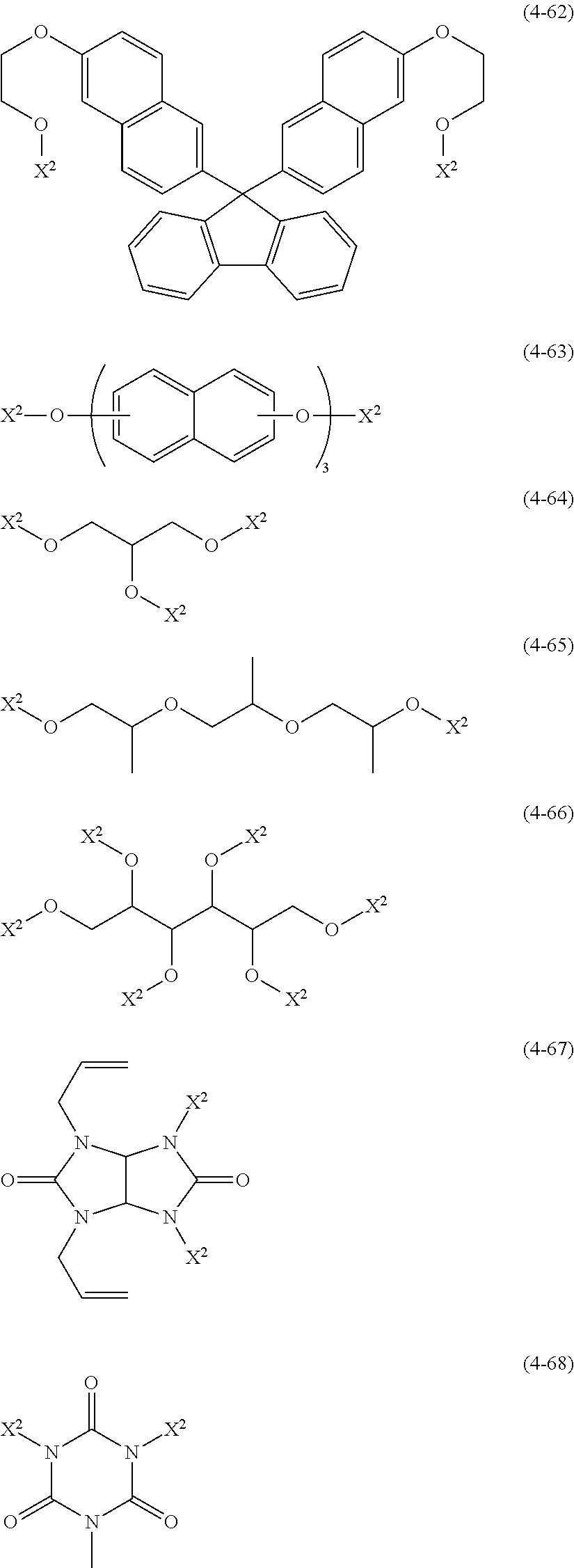

W


W

W

W

W


W


W


Applications Claiming Priority (2)
| Application Number | Priority Date | Filing Date | Title |
|---|---|---|---|
| JP2016134895 | 2016-07-07 | ||
| JP2016-134895 | 2016-07-07 |
Publications (2)
| Publication Number | Publication Date |
|---|---|
| US20180011405A1 US20180011405A1 (en) | 2018-01-11 |
| US10620537B2 true US10620537B2 (en) | 2020-04-14 |
Family
ID=60910367
Family Applications (1)
| Application Number | Title | Priority Date | Filing Date |
|---|---|---|---|
| US15/621,482 Active US10620537B2 (en) | 2016-07-07 | 2017-06-13 | Resist underlayer film composition, patterning process, method for forming resist underlayer film, and compound for resist underlayer film composition |
Country Status (5)
| Country | Link |
|---|---|
| US (1) | US10620537B2 (en) |
| JP (1) | JP6697416B2 (en) |
| KR (1) | KR101953976B1 (en) |
| CN (1) | CN107589633B (en) |
| TW (1) | TWI641914B (en) |
Families Citing this family (19)
| Publication number | Priority date | Publication date | Assignee | Title |
|---|---|---|---|---|
| JP6714492B2 (en) * | 2015-12-24 | 2020-06-24 | 信越化学工業株式会社 | Organic film forming compound, organic film forming composition, organic film forming method, and pattern forming method |
| JP6714493B2 (en) | 2015-12-24 | 2020-06-24 | 信越化学工業株式会社 | Organic film forming compound, organic film forming composition, organic film forming method, and pattern forming method |
| US11086220B2 (en) * | 2017-10-31 | 2021-08-10 | Rohm And Haas Electronic Materials Korea Ltd. | Underlayer coating compositions for use with photoresists |
| JP6910319B2 (en) * | 2018-04-23 | 2021-07-28 | 東京エレクトロン株式会社 | How to etch the organic region |
| KR102264693B1 (en) | 2018-06-11 | 2021-06-11 | 삼성에스디아이 주식회사 | Resist underlayer composition, and method of forming patterns using the composition |
| KR102278459B1 (en) * | 2018-08-21 | 2021-07-16 | 삼성에스디아이 주식회사 | Polymer, organic layer composition and method of forming patterns |
| KR102668667B1 (en) * | 2019-02-21 | 2024-05-24 | 동우 화인켐 주식회사 | Resist stripper composition |
| JP7271461B2 (en) * | 2020-02-19 | 2023-05-11 | 信越化学工業株式会社 | Organic film forming material and pattern forming method |
| JP7316237B2 (en) | 2020-03-02 | 2023-07-27 | 信越化学工業株式会社 | Organic film forming material, organic film forming method, pattern forming method and compound |
| CN119472173A (en) * | 2020-06-12 | 2025-02-18 | 日产化学株式会社 | Resist underlayer film-forming composition containing diol structure |
| JP7368322B2 (en) * | 2020-06-12 | 2023-10-24 | 信越化学工業株式会社 | Resist underlayer film material, pattern forming method, and resist underlayer film forming method |
| JP7445583B2 (en) * | 2020-11-25 | 2024-03-07 | 信越化学工業株式会社 | Resist underlayer film material, pattern forming method, and resist underlayer film forming method |
| US12379660B2 (en) | 2020-12-18 | 2025-08-05 | Dupont Electronic Materials International, Llc | Adhesion promoting photoresist underlayer composition |
| JP7541939B2 (en) * | 2021-02-15 | 2024-08-29 | 信越化学工業株式会社 | Material for forming organic film, substrate for manufacturing semiconductor device, method for forming organic film, method for forming pattern, and compound for forming organic film |
| WO2022210901A1 (en) * | 2021-03-31 | 2022-10-06 | 日産化学株式会社 | Composition for forming silicon-containing resist underlayer film |
| JP7690417B2 (en) * | 2022-02-25 | 2025-06-10 | 信越化学工業株式会社 | Planarizing agent for forming organic film, composition for forming organic film, method for forming organic film, and method for forming pattern |
| JP7698607B2 (en) * | 2022-06-10 | 2025-06-25 | 信越化学工業株式会社 | Resist underlayer film material, pattern forming method, and resist underlayer film forming method |
| EP4435516A1 (en) * | 2023-03-16 | 2024-09-25 | Shin-Etsu Chemical Co., Ltd. | Method for forming resist underlayer film and patterning process |
| JP2025144983A (en) * | 2024-03-21 | 2025-10-03 | 株式会社Screenホールディングス | Substrate processing method and substrate processing apparatus |
Citations (20)
| Publication number | Priority date | Publication date | Assignee | Title |
|---|---|---|---|---|
| US4824892A (en) * | 1984-10-18 | 1989-04-25 | Riedel-De Haen Aktiengesellschaft | UV light stabilizer based on benzophenone |
| US20020106909A1 (en) | 2001-02-07 | 2002-08-08 | Hitoshi Kato | Silicon nitride film forming method, silicon nitride film forming system and silicon nitride film forming system precleaning method |
| JP2002334869A (en) | 2001-02-07 | 2002-11-22 | Tokyo Electron Ltd | Method and apparatus for forming silicon nitride film and pre-cleaning method for the apparatus |
| JP2004205685A (en) | 2002-12-24 | 2004-07-22 | Shin Etsu Chem Co Ltd | Pattern forming method and underlayer film forming material |
| WO2004066377A1 (en) | 2003-01-24 | 2004-08-05 | Tokyo Electron Limited | Method of cvd for forming silicon nitride film on substrate |
| US20070078198A1 (en) * | 2003-05-23 | 2007-04-05 | Atsuo Otsuji | (Meth) acrylic ester compound and use thereof |
| JP2007199653A (en) | 2005-12-27 | 2007-08-09 | Shin Etsu Chem Co Ltd | Photoresist underlayer film forming material and pattern forming method |
| US20070231745A1 (en) * | 2006-03-31 | 2007-10-04 | Fujifilm Corporation | Method for preparation of lithographic printing plate and lithographic printing plate precursor |
| US20080318188A1 (en) * | 2004-04-28 | 2008-12-25 | The Regents Of The University Of Colorado | Dimer Acid-Derived Dimethacrylates and Use in Dental Restorative Compositions |
| US20090274978A1 (en) | 2008-05-01 | 2009-11-05 | Masaki Ohashi | Novel photoacid generator, resist composition, and patterning process |
| JP2010078729A (en) | 2008-09-24 | 2010-04-08 | Fujifilm Corp | Photosensitive resin composition, color filter and method for manufacturing the same, and solid imaging element |
| JP2010093065A (en) * | 2008-10-08 | 2010-04-22 | Fujifilm Corp | Curing composition for optical nanoimprint, cured material using the same and manufacturing method thereby, and member for liquid crystal display device |
| US20120041102A1 (en) * | 2009-04-24 | 2012-02-16 | Korea Institute Of Industrial Technology | Novel epoxy resin and epoxy resin composition comprising the same |
| US20120145971A1 (en) * | 2010-12-10 | 2012-06-14 | Cheil Industries Inc. | Photosensitive Resin Composition and Light Blocking Layer Using the Same |
| JP5141858B2 (en) | 2006-09-19 | 2013-02-13 | 日産化学工業株式会社 | Electron beam curing resist underlayer film forming composition |
| US20130302990A1 (en) | 2012-05-08 | 2013-11-14 | Shin-Etsu Chemical Co., Ltd. | Organic film composition, method for forming organic film and patterning process using this, and heat-decomposable polymer |
| US20130303655A1 (en) * | 2011-01-31 | 2013-11-14 | 3M Innovative Properties Company | Dental composition, method of producing and use thereof |
| JP2015040224A (en) * | 2013-08-20 | 2015-03-02 | 大阪ガスケミカル株式会社 | Multifunctional (meth) acrylate with fluorene skeleton |
| WO2015168771A1 (en) * | 2014-05-05 | 2015-11-12 | Centre De Technologie Minerale Et De Plasturgie Inc. | Cardanol glycidyl ether derivatives |
| US20170144954A1 (en) * | 2014-05-08 | 2017-05-25 | Mitsubishi Gas Chemical Company, Inc. | Material for forming film for lithography, composition for forming film for lithography, film for lithography, pattern forming method and purification method |
Family Cites Families (11)
| Publication number | Priority date | Publication date | Assignee | Title |
|---|---|---|---|---|
| JPS5833506B2 (en) | 1974-10-04 | 1983-07-20 | ミノルタ株式会社 | digital circuit tester |
| US7625695B2 (en) * | 2006-08-24 | 2009-12-01 | Samsung Electronics Co., Ltd. | Polymers for anti-reflective coatings, anti-reflective coating compositions and methods of forming a pattern using the same |
| US8173415B2 (en) * | 2008-10-10 | 2012-05-08 | Mcmaster University | Single cell microinjection using flexible and compliant fluidic channels and electroosmotic dosage control |
| JP5068831B2 (en) * | 2010-02-05 | 2012-11-07 | 信越化学工業株式会社 | Resist underlayer film material, resist underlayer film forming method, pattern forming method |
| JP5794228B2 (en) * | 2010-03-31 | 2015-10-14 | Jsr株式会社 | Composition for forming a resist underlayer film |
| JP5595151B2 (en) * | 2010-07-13 | 2014-09-24 | キヤノン株式会社 | Image processing apparatus, compression method in image processing apparatus, and program |
| JP5266294B2 (en) * | 2010-11-01 | 2013-08-21 | 信越化学工業株式会社 | Resist underlayer film material and pattern forming method using the same |
| JP5485185B2 (en) * | 2011-01-05 | 2014-05-07 | 信越化学工業株式会社 | Resist underlayer film material and pattern forming method using the same |
| AU2011361577B2 (en) * | 2011-03-09 | 2017-04-20 | Irdeto B.V. | Method and system for dynamic platform security in a device operating system |
| KR101855506B1 (en) * | 2011-10-13 | 2018-05-08 | 주식회사 동진쎄미켐 | Polymer having aromatic ring and under-layer composition of resist including the same |
| JP5894106B2 (en) * | 2012-06-18 | 2016-03-23 | 信越化学工業株式会社 | Compound for forming resist underlayer film, resist underlayer film material using the same, resist underlayer film forming method, pattern forming method |
-
2017
- 2017-05-29 JP JP2017105225A patent/JP6697416B2/en active Active
- 2017-06-13 US US15/621,482 patent/US10620537B2/en active Active
- 2017-07-04 KR KR1020170084625A patent/KR101953976B1/en active Active
- 2017-07-05 TW TW106122461A patent/TWI641914B/en active
- 2017-07-06 CN CN201710546915.6A patent/CN107589633B/en active Active
Patent Citations (23)
| Publication number | Priority date | Publication date | Assignee | Title |
|---|---|---|---|---|
| US4824892A (en) * | 1984-10-18 | 1989-04-25 | Riedel-De Haen Aktiengesellschaft | UV light stabilizer based on benzophenone |
| US20020106909A1 (en) | 2001-02-07 | 2002-08-08 | Hitoshi Kato | Silicon nitride film forming method, silicon nitride film forming system and silicon nitride film forming system precleaning method |
| JP2002334869A (en) | 2001-02-07 | 2002-11-22 | Tokyo Electron Ltd | Method and apparatus for forming silicon nitride film and pre-cleaning method for the apparatus |
| JP2004205685A (en) | 2002-12-24 | 2004-07-22 | Shin Etsu Chem Co Ltd | Pattern forming method and underlayer film forming material |
| WO2004066377A1 (en) | 2003-01-24 | 2004-08-05 | Tokyo Electron Limited | Method of cvd for forming silicon nitride film on substrate |
| US20050255712A1 (en) | 2003-01-24 | 2005-11-17 | Tokyo Electronlimited | Method of cvd for forming silicon nitride film on substrate |
| US20070078198A1 (en) * | 2003-05-23 | 2007-04-05 | Atsuo Otsuji | (Meth) acrylic ester compound and use thereof |
| US20080318188A1 (en) * | 2004-04-28 | 2008-12-25 | The Regents Of The University Of Colorado | Dimer Acid-Derived Dimethacrylates and Use in Dental Restorative Compositions |
| JP2007199653A (en) | 2005-12-27 | 2007-08-09 | Shin Etsu Chem Co Ltd | Photoresist underlayer film forming material and pattern forming method |
| US20070231745A1 (en) * | 2006-03-31 | 2007-10-04 | Fujifilm Corporation | Method for preparation of lithographic printing plate and lithographic printing plate precursor |
| JP5141858B2 (en) | 2006-09-19 | 2013-02-13 | 日産化学工業株式会社 | Electron beam curing resist underlayer film forming composition |
| US20090274978A1 (en) | 2008-05-01 | 2009-11-05 | Masaki Ohashi | Novel photoacid generator, resist composition, and patterning process |
| JP2009269953A (en) | 2008-05-01 | 2009-11-19 | Shin Etsu Chem Co Ltd | New photoacid generator, resist material using the same, and pattern forming method |
| JP2010078729A (en) | 2008-09-24 | 2010-04-08 | Fujifilm Corp | Photosensitive resin composition, color filter and method for manufacturing the same, and solid imaging element |
| JP2010093065A (en) * | 2008-10-08 | 2010-04-22 | Fujifilm Corp | Curing composition for optical nanoimprint, cured material using the same and manufacturing method thereby, and member for liquid crystal display device |
| US20120041102A1 (en) * | 2009-04-24 | 2012-02-16 | Korea Institute Of Industrial Technology | Novel epoxy resin and epoxy resin composition comprising the same |
| US20120145971A1 (en) * | 2010-12-10 | 2012-06-14 | Cheil Industries Inc. | Photosensitive Resin Composition and Light Blocking Layer Using the Same |
| US20130303655A1 (en) * | 2011-01-31 | 2013-11-14 | 3M Innovative Properties Company | Dental composition, method of producing and use thereof |
| US20130302990A1 (en) | 2012-05-08 | 2013-11-14 | Shin-Etsu Chemical Co., Ltd. | Organic film composition, method for forming organic film and patterning process using this, and heat-decomposable polymer |
| JP2013253227A (en) | 2012-05-08 | 2013-12-19 | Shin-Etsu Chemical Co Ltd | Organic film material, method for forming organic film and method for forming pattern using the same, and heat-decomposable polymer |
| JP2015040224A (en) * | 2013-08-20 | 2015-03-02 | 大阪ガスケミカル株式会社 | Multifunctional (meth) acrylate with fluorene skeleton |
| WO2015168771A1 (en) * | 2014-05-05 | 2015-11-12 | Centre De Technologie Minerale Et De Plasturgie Inc. | Cardanol glycidyl ether derivatives |
| US20170144954A1 (en) * | 2014-05-08 | 2017-05-25 | Mitsubishi Gas Chemical Company, Inc. | Material for forming film for lithography, composition for forming film for lithography, film for lithography, pattern forming method and purification method |
Non-Patent Citations (4)
| Title |
|---|
| English translation of JP-2010-093065 A, published Apr. 22, 2010, the translation was generated Mar. 4, 2018, 36 pages at INPIT website. * |
| English translation of JP-2015-40224 A, published Mar. 2, 2015 , the translation was generated Mar. 4, 2018, 51 pages at INPIT website. * |
| May 1, 2018 Office Action issued in Korean Patent Application No. 2017-0084625. |
| Mc Grath et al "PHoto-curable polymers based upon methacrylates and diemthacrylate contaiing carbazole", Polymer Preprints year 2000, vol. 41, No. 2, pp. 1363-1364. (Year: 2000). * |
Also Published As
| Publication number | Publication date |
|---|---|
| KR20180006313A (en) | 2018-01-17 |
| CN107589633B (en) | 2020-11-13 |
| US20180011405A1 (en) | 2018-01-11 |
| TW201809889A (en) | 2018-03-16 |
| KR101953976B1 (en) | 2019-05-23 |
| TWI641914B (en) | 2018-11-21 |
| JP6697416B2 (en) | 2020-05-20 |
| JP2018013768A (en) | 2018-01-25 |
| CN107589633A (en) | 2018-01-16 |
Similar Documents
| Publication | Publication Date | Title |
|---|---|---|
| US10620537B2 (en) | Resist underlayer film composition, patterning process, method for forming resist underlayer film, and compound for resist underlayer film composition | |
| US9296922B2 (en) | Stable metal compounds as hardmasks and filling materials, their compositions and methods of use | |
| US9372404B2 (en) | Organic film composition, method for forming organic film and patterning process using this, and heat-decomposable polymer | |
| US12147160B2 (en) | Resist underlayer film material, patterning process, and method for forming resist underlayer film | |
| US10189947B2 (en) | Composition of anti-reflective hardmask | |
| JP5768410B2 (en) | Near infrared light absorbing film forming material and laminated film | |
| JP6818138B2 (en) | High etching resistance spin-on carbon hard mask composition and patterning method using it | |
| US12013640B2 (en) | Resist underlayer film material, patterning process, and method for forming resist underlayer film | |
| US20160229939A1 (en) | Silicon-containing polymer, silicon-containing compound, composition for forming a resist under layer film, and patterning process | |
| US9312144B2 (en) | Composition for forming a silicon-containing resist under layer film and patterning process | |
| CN116478617B (en) | Protective film forming composition for alkaline hydrogen peroxide solution, substrate for semiconductor device manufacturing, and protective film forming method | |
| US12498639B2 (en) | Material for forming adhesive film, method for forming adhesive film using the same, and patterning process using material for forming adhesive film | |
| CN116157436A (en) | Composition for forming underlayer film for lithography, underlayer film, and pattern forming method | |
| US20240295816A1 (en) | Compound For Forming Metal-Containing Film, Composition For Forming Metal-Containing Film, And Patterning Process | |
| JP2024116011A (en) | Pattern Formation Method | |
| WO2023032998A1 (en) | Spin-on-carbon film-forming composition, method for producing spin-on-carbon film-forming composition, lithographic underlayer film, method for forming resist pattern, and method for forming circuit pattern | |
| US20250297127A1 (en) | Composition for forming organic film, method for forming organic film, patterning process, monomer, and polymer | |
| US20250271763A1 (en) | Composition for Forming Organic Film, Method for Forming Organic Film and Patterning Process | |
| JP7258279B2 (en) | Film-forming material for lithography, film-forming composition for lithography, underlayer film for lithography, and pattern forming method | |
| WO2024005194A1 (en) | Polyphenol compound, film-forming composition for lithography, underlayer film for lithography, and method for forming pattern |
Legal Events
| Date | Code | Title | Description |
|---|---|---|---|
| AS | Assignment |
Owner name: SHIN-ETSU CHEMICAL CO., LTD., JAPAN Free format text: ASSIGNMENT OF ASSIGNORS INTEREST;ASSIGNORS:WATANABE, TAKERU;KIKUCHI, RIE;KORI, DAISUKE;AND OTHERS;SIGNING DATES FROM 20170518 TO 20170522;REEL/FRAME:042695/0111 |
|
| STPP | Information on status: patent application and granting procedure in general |
Free format text: NON FINAL ACTION MAILED |
|
| STPP | Information on status: patent application and granting procedure in general |
Free format text: RESPONSE TO NON-FINAL OFFICE ACTION ENTERED AND FORWARDED TO EXAMINER |
|
| STPP | Information on status: patent application and granting procedure in general |
Free format text: FINAL REJECTION MAILED |
|
| STPP | Information on status: patent application and granting procedure in general |
Free format text: ADVISORY ACTION MAILED |
|
| STPP | Information on status: patent application and granting procedure in general |
Free format text: RESPONSE AFTER FINAL ACTION FORWARDED TO EXAMINER |
|
| STPP | Information on status: patent application and granting procedure in general |
Free format text: NOTICE OF ALLOWANCE MAILED -- APPLICATION RECEIVED IN OFFICE OF PUBLICATIONS |
|
| STPP | Information on status: patent application and granting procedure in general |
Free format text: PUBLICATIONS -- ISSUE FEE PAYMENT VERIFIED |
|
| STCF | Information on status: patent grant |
Free format text: PATENTED CASE |
|
| MAFP | Maintenance fee payment |
Free format text: PAYMENT OF MAINTENANCE FEE, 4TH YEAR, LARGE ENTITY (ORIGINAL EVENT CODE: M1551); ENTITY STATUS OF PATENT OWNER: LARGE ENTITY Year of fee payment: 4 |