US10620300B2 - SPAD array with gated histogram construction - Google Patents
SPAD array with gated histogram construction Download PDFInfo
- Publication number
- US10620300B2 US10620300B2 US14/830,760 US201514830760A US10620300B2 US 10620300 B2 US10620300 B2 US 10620300B2 US 201514830760 A US201514830760 A US 201514830760A US 10620300 B2 US10620300 B2 US 10620300B2
- Authority
- US
- United States
- Prior art keywords
- sensing element
- sensing
- during
- sequence
- acquisition periods
- Prior art date
- Legal status (The legal status is an assumption and is not a legal conclusion. Google has not performed a legal analysis and makes no representation as to the accuracy of the status listed.)
- Active, expires
Links
Images


Classifications
-
- G—PHYSICS
- G01—MEASURING; TESTING
- G01S—RADIO DIRECTION-FINDING; RADIO NAVIGATION; DETERMINING DISTANCE OR VELOCITY BY USE OF RADIO WAVES; LOCATING OR PRESENCE-DETECTING BY USE OF THE REFLECTION OR RERADIATION OF RADIO WAVES; ANALOGOUS ARRANGEMENTS USING OTHER WAVES
- G01S7/00—Details of systems according to groups G01S13/00, G01S15/00, G01S17/00
- G01S7/48—Details of systems according to groups G01S13/00, G01S15/00, G01S17/00 of systems according to group G01S17/00
- G01S7/483—Details of pulse systems
- G01S7/486—Receivers
- G01S7/4865—Time delay measurement, e.g. time-of-flight measurement, time of arrival measurement or determining the exact position of a peak
-
- G—PHYSICS
- G01—MEASURING; TESTING
- G01S—RADIO DIRECTION-FINDING; RADIO NAVIGATION; DETERMINING DISTANCE OR VELOCITY BY USE OF RADIO WAVES; LOCATING OR PRESENCE-DETECTING BY USE OF THE REFLECTION OR RERADIATION OF RADIO WAVES; ANALOGOUS ARRANGEMENTS USING OTHER WAVES
- G01S17/00—Systems using the reflection or reradiation of electromagnetic waves other than radio waves, e.g. lidar systems
- G01S17/02—Systems using the reflection of electromagnetic waves other than radio waves
- G01S17/06—Systems determining position data of a target
- G01S17/08—Systems determining position data of a target for measuring distance only
- G01S17/10—Systems determining position data of a target for measuring distance only using transmission of interrupted, pulse-modulated waves
-
- G01S17/107—
-
- G—PHYSICS
- G01—MEASURING; TESTING
- G01S—RADIO DIRECTION-FINDING; RADIO NAVIGATION; DETERMINING DISTANCE OR VELOCITY BY USE OF RADIO WAVES; LOCATING OR PRESENCE-DETECTING BY USE OF THE REFLECTION OR RERADIATION OF RADIO WAVES; ANALOGOUS ARRANGEMENTS USING OTHER WAVES
- G01S17/00—Systems using the reflection or reradiation of electromagnetic waves other than radio waves, e.g. lidar systems
- G01S17/02—Systems using the reflection of electromagnetic waves other than radio waves
- G01S17/06—Systems determining position data of a target
- G01S17/08—Systems determining position data of a target for measuring distance only
- G01S17/10—Systems determining position data of a target for measuring distance only using transmission of interrupted, pulse-modulated waves
- G01S17/18—Systems determining position data of a target for measuring distance only using transmission of interrupted, pulse-modulated waves wherein range gates are used
-
- G—PHYSICS
- G01—MEASURING; TESTING
- G01S—RADIO DIRECTION-FINDING; RADIO NAVIGATION; DETERMINING DISTANCE OR VELOCITY BY USE OF RADIO WAVES; LOCATING OR PRESENCE-DETECTING BY USE OF THE REFLECTION OR RERADIATION OF RADIO WAVES; ANALOGOUS ARRANGEMENTS USING OTHER WAVES
- G01S17/00—Systems using the reflection or reradiation of electromagnetic waves other than radio waves, e.g. lidar systems
- G01S17/88—Lidar systems specially adapted for specific applications
- G01S17/89—Lidar systems specially adapted for specific applications for mapping or imaging
- G01S17/894—Three-dimensional [3D] imaging with simultaneous measurement of time-of-flight at a two-dimensional [2D] array of receiver pixels, e.g. time-of-flight cameras or flash lidar
-
- G—PHYSICS
- G01—MEASURING; TESTING
- G01S—RADIO DIRECTION-FINDING; RADIO NAVIGATION; DETERMINING DISTANCE OR VELOCITY BY USE OF RADIO WAVES; LOCATING OR PRESENCE-DETECTING BY USE OF THE REFLECTION OR RERADIATION OF RADIO WAVES; ANALOGOUS ARRANGEMENTS USING OTHER WAVES
- G01S7/00—Details of systems according to groups G01S13/00, G01S15/00, G01S17/00
- G01S7/48—Details of systems according to groups G01S13/00, G01S15/00, G01S17/00 of systems according to group G01S17/00
- G01S7/483—Details of pulse systems
- G01S7/486—Receivers
- G01S7/4861—Circuits for detection, sampling, integration or read-out
- G01S7/4863—Detector arrays, e.g. charge-transfer gates
-
- G—PHYSICS
- G04—HOROLOGY
- G04F—TIME-INTERVAL MEASURING
- G04F10/00—Apparatus for measuring unknown time intervals by electric means
- G04F10/005—Time-to-digital converters [TDC]
-
- H01L31/02027—
-
- H—ELECTRICITY
- H10—SEMICONDUCTOR DEVICES; ELECTRIC SOLID-STATE DEVICES NOT OTHERWISE PROVIDED FOR
- H10F—INORGANIC SEMICONDUCTOR DEVICES SENSITIVE TO INFRARED RADIATION, LIGHT, ELECTROMAGNETIC RADIATION OF SHORTER WAVELENGTH OR CORPUSCULAR RADIATION
- H10F77/00—Constructional details of devices covered by this subclass
- H10F77/95—Circuit arrangements
- H10F77/953—Circuit arrangements for devices having potential barriers
- H10F77/959—Circuit arrangements for devices having potential barriers for devices working in avalanche mode
Definitions
- the present invention relates generally to electronic imaging, and particularly to devices and methods for depth mapping based on time-of-flight measurement.
- Time-of-flight (TOF) imaging techniques are used in many depth mapping systems (also referred to as 3D mapping or 3D imaging).
- a light source such as a pulsed laser
- direct TOF techniques directs pulses of optical radiation toward the scene that is to be mapped
- a high-speed detector senses the time of arrival of the radiation reflected from the scene.
- the depth value at each pixel in the depth map is derived from the difference between the emission time of the outgoing pulse and the arrival time of the reflected radiation from the corresponding point in the scene, which is referred to as the “time of flight” of the optical pulses.
- Single-photon avalanche diodes also known as Geiger-mode avalanche photodiodes (GAPDs)
- GPDs Geiger-mode avalanche photodiodes
- SPAD sensors are detectors capable of capturing individual photons with very high time-of-arrival resolution, of the order of a few tens of picoseconds. They may be fabricated in dedicated semiconductor processes or in standard CMOS technologies. Arrays of SPAD sensors, fabricated on a single chip, have been used experimentally in 3D imaging cameras. Charbon et al. provide a useful review of SPAD technologies in “SPAD-Based Sensors,” published in TOF Range - Imaging Cameras (Springer-Verlag, 2013), which is incorporated herein by reference.
- TCSPC time-correlated single-photon counting
- Embodiments of the present invention that are described hereinbelow provide improved methods and devices for time of arrival sensing.
- a sensing device including a first array of sensing elements. Each sensing element is configured to output a signal indicative of a time of incidence of a single photon on the sensing element during a certain gating interval in each of a succession acquisition periods.
- a second array of processing circuits are coupled respectively to the sensing elements.
- the processing circuits include a gating generator, which is configured to variably set a start time of the gating interval for each sensing element within each acquisition period, and a memory, which is coupled to record the time of incidence of the single photon on each sensing element in each acquisition period, responsively to the signal.
- a controller is configured to control the gating generator during a first sequence of the acquisition periods so as to sweep the gating interval over the acquisition periods and to identify, responsively to the signal from each sensing element during the first sequence of the acquisition periods, a respective detection window for the sensing element, and during a second sequence of the acquisition periods, following the first sequence, to fix the gating interval for each sensing element to coincide with the respective detection window.
- the sensing elements include single-photon avalanche diodes (SPADs).
- SPADs single-photon avalanche diodes
- the first array includes a first two-dimensional matrix of the sensing elements formed on a first semiconductor chip
- the second array includes a second two-dimensional matrix of the processing circuits formed on a second semiconductor chip and coupled to the first matrix in a one-to-one correspondence between the sensing elements and the processing circuits.
- the processing circuits are configured to set different, respective detection windows for different ones of the sensing elements. Additionally or alternatively, the processing circuits are configured to sweep the gating interval during the first sequence of the acquisition periods during each frame among a series of image frames, to identify the respective detection window for each sensing element in each frame, responsively to the signal during the first sequence of the acquisition periods in the frame, such that the detection window for at least some of the sensing elements changes over the series of the image frames.
- the processing circuits include a respective time-to-digital converter (TDC) coupled to receive the signal from each sensing element and to increment, responsively to the signal, a count in the memory of respective times of incidence of photons on the sensing element.
- TDC time-to-digital converter
- the memory is configured to store respective counts of the photons that arrive in a plurality of different time bins within the detection window during the second sequence of the acquisition periods.
- the controller is configured to process a histogram of the respective counts over the different time bins for each sensing element so as to derive and output a respective time-of-arrival value for the sensing element.
- the device includes a radiation source, which is configured to direct a train of pulses of radiation, synchronized with the acquisition periods, toward an object, wherein the sensing elements are configured to detect photons of the radiation reflected from the object, and wherein the processing circuits are configured to measure times of flight of the photons.
- a method for sensing which includes providing a first array of sensing elements, each sensing element configured to output a signal indicative of a time of incidence of a single photon on the sensing element during a certain gating interval in each of a succession acquisition periods.
- a second array of processing circuits are coupled respectively to the sensing elements.
- the processing circuits include a gating generator, which is configured to variably set a start time of the gating interval for each sensing element within each acquisition period, and a memory, which is coupled to record the time of incidence of the single photon on each sensing element in each acquisition period, responsively to the signal.
- the gating generator is controlled during a first sequence of the acquisition periods so as to sweep the gating interval over the acquisition periods. Responsively to the signal from each sensing element during the first sequence of the acquisition periods, a respective detection window is identified for each sensing element. During a second sequence of the acquisition periods, following the first sequence, the gating generator is controlled so as to fix the gating interval for each sensing element to coincide with the respective detection window.
- FIG. 1 is a schematic side view of a depth mapping device, in accordance with an embodiment of the invention.
- FIG. 2 is a block diagram showing components of a pixel in a SPAD array, in accordance with an embodiment of the invention
- FIG. 3 is a flow chart that schematically illustrates a method for TOF measurement, in accordance with an embodiment of the invention
- FIG. 4 is a timing diagram, which schematically illustrates phases in the operation of a SPAD sensor, in accordance with an embodiment of the invention
- FIG. 5 is a plot that schematically shows signals associated with the operation of a depth mapping device, in accordance with an embodiment of the invention.
- FIG. 6 is a plot that schematically illustrates a histogram generated by a SPAD sensor, in accordance with an embodiment of the invention.
- a histogram of photon arrival times must be created for each pixel, and then processed in order to extract the TOF value for that pixel.
- the precision of the TOF measurement, and hence of the depth values in the map depends upon the temporal resolution of the histogram bins. Therefore, to achieve high precision over a large depth range, a very large histogram memory would be required. For a single SPAD or a small array, this memory can be separated from the SPAD detection area. For larger SPAD arrays, however, practical designs require that the memory for each pixel be immediately adjacent to the sensor area of the pixel. Limitations on pixel size, however, place a severe limit on the size of the memory in each pixel, and thus on the temporal resolution of TOF measurement.
- Embodiments of the present invention that are described herein address this problem by using adaptively gated detection, so that memory resources are applied selectively at each pixel in each depth mapping frame.
- each frame is divided into two phases: a coarse measurement phase, in which the approximate TOF value for the pixel is estimated, followed by a fine measurement phase, in which a TOF histogram is captured within a narrow measurement window that is set on the basis of the approximate TOF found in the coarse phase.
- the histogram can thus be constructed with high resolution within the measurement window, while ignoring arrival times outside the measurement window and thus limiting the size of the memory required in each pixel.
- the use of this sort of gated detection is also advantageous in reducing the effect of background photons on TOF measurement, since photons arriving at the sensing elements before the gating period in any given acquisition period will be ignored.
- the disclosed embodiments provide a sensing device, comprising an array of sensing elements, such as SPADs, and an array of processing circuits, which are coupled respectively to the sensing elements.
- the SPADs are gated by gating generators in the corresponding processing circuits, and thus detect photons only during a certain gating interval, which can be varied from one acquisition period to the next.
- Each acquisition period is timed to begin, for example, when a radiation source, such as a laser, outputs a pulse of radiation, and each measurement frame of the sensing device comprises a succession of many such acquisition periods.
- a controller chooses the gating interval for each pixel in each acquisition period and instructs the gating generator to set the start time of the gating interval accordingly.
- Each sensing element then outputs a signal indicative of the time of incidence of a single photon on the sensing element during the gating interval.
- the processing circuits also comprise a memory, which records the time of incidence of the single photon on each sensing element in each acquisition period.
- the controller is responsible for implementing the coarse and fine measurement phases.
- the controller In the coarse measurement phase, covering a first sequence of acquisition periods in each frame, the controller sweeps the gating interval over the acquisition periods, in order to test a range of different gating intervals. Based on the signals output by the sensing elements during this first sequence of the acquisition periods, the controller identifies a respective detection window for each sensing element, which typically corresponds to the gating interval in which the largest number of photons was received. The detection window thus identified for each sensing element gives the TOF for the corresponding pixel with coarse resolution.
- the fine measurement phase begins, comprising a second sequence of acquisition periods, following the first sequence.
- the controller fixes the gating interval for each sensing element to coincide with the respective detection window that was found in the coarse measurement phase.
- the detection windows will differ from pixel to pixel, and the gating intervals of different sensing elements are accordingly set to different values during the fine measurement phase.
- the detection window that is identified for each pixel during the coarse measurement phase of each frame, and thus the detection window that is applied in the fine measurement phase can typically change over the series of the image frames.
- the processing circuits coupled to each SPAD sensing element in the array comprise a respective time-to-digital converter (TDC).
- TDC time-to-digital converter
- the TDC increments counts in the pixel memory of the respective times of incidence of photons on the sensing element.
- the memory of each pixel stores respective counts of the photons that arrive at the sensing element in multiple different time bins, which span the detection window that the controller set for this pixel.
- the controller processes the histogram of the respective counts stored in the pixel memory in order to derive and output the respective time-of-arrival value for the corresponding sensing element.
- the sensing elements are arranged in a two-dimensional matrix array, formed on a semiconductor chip.
- the processing circuits are also arranged in a two-dimensional matrix, typically on a second semiconductor chip, and are coupled to the matrix of sensing elements in a one-to-one correspondence, using chip stacking techniques, for example.
- the sensing elements and processing circuits may be fabricated together on a single chip.
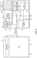
- FIG. 1 is a schematic side view of a depth mapping device 20 , in accordance with an embodiment of the invention.
- device 20 is used to generate depth maps of an object 22 , for example a part of the body of a user of the device for purposes of gesture recognition.
- an illumination assembly 24 directs pulses of light toward object 22
- an imaging assembly 26 measures the TOF of the photons reflected from the object.
- Illumination assembly 24 typically comprises a pulsed laser 28 , which emits short pulses of light, with pulse duration in the picosecond range and repetition frequency in the range of 1-10 MHz. Collection optics 30 direct the light toward object 22 . Alternatively, other pulse durations and repetition frequencies may be used, depending on application requirements.
- Imaging assembly 26 comprises objective optics 32 , which image object 22 onto a sensing array 34 , so that photons emitted by illumination assembly 24 and reflected from object 22 are incident on the sensing device.
- sensing array 34 comprises a sensor chip 36 and a processing chip 38 , which are coupled together, for example, using chip stacking techniques that are known in the art.
- Sensor chip 36 comprises an array of sensing elements 40 , such as SPAD sensors, each of which outputs a signal indicative of a time of incidence of a single photon on the sensing element during a gating interval in each of a succession of acquisition periods.
- Processing chip 38 comprises an array of processing circuits 42 , which are coupled respectively to the sensing elements.
- Both of chips 36 and 38 may be produced from silicon wafers using well-known CMOS fabrication processes, based on SPAD sensor designs that are known in the art, along with accompanying drive circuits, logic and memory as described herein. Alternatively, the designs and principles of detection that are described herein may be implemented, mutatis mutandis, using other materials and processes. All such alternative implementations are considered to be within the scope of the present invention.
- Imaging device 20 is timed to capture TOF information continually over a series of image frames, for example at a rate of thirty frames/sec.
- each of processing circuits 42 counts photons that are incident on the corresponding sensing element 40 in a plurality of different time bins and constructs a histogram of the respective counts over the different time bins, using coarse and fine measurement phase as noted above. On the basis of this histogram, each processing circuit derives and outputs a respective time-of-arrival value for its corresponding sensing element.
- a system controller 44 reads out the individual pixel values and generates an output depth map, comprising the measured TOF—or equivalently, the measured depth value—at each pixel.
- the depth map is typically conveyed to a receiving device 46 , such as a display or a computer or other processor, which segments and extracts high-level information from the depth map.
- FIG. 2 is a block diagram showing components of a detection pixel 50 , comprising a single sensing element 40 and the corresponding processing circuit 42 for a single pixel in sensing array 34 , in accordance with an embodiment of the invention.
- Sensing element 40 comprises a SPAD 52 , with peripheral circuits 54 that issue driving signals to the SPAD, such as quenching and gating signals.
- peripheral circuits 54 are located on the same chip 36 as SPAD 52 , but the peripheral circuits may alternatively be located on processing chip 38 with suitable inter-chip connections.
- SPAD 52 generates output pulses (SPAD OUT) in response to incident photons only during short gating intervals that are defined by the driving signals from peripheral circuits 54 . Photons incident outside the gating interval have no effect on the SPAD output.
- SPAD OUT output pulses
- Processing circuit 42 for each sensing element 40 comprises logic circuits that provide the necessary timing signals to sensing element 40 (SPAD EN) and process the pulses output by SPAD 52 (SPAD OUT).
- Processing circuit 42 comprises a gating signal generator 56 , which comprises, in the present example, a shift register 58 , such as an eight-bit shift register, with a multiplexer 60 to produce output pulses at the time within each acquisition interval that is indicated by the shift register value.
- gating signal generator 56 may comprise a counter and decoder, a look-up table, or other suitable components that are known in the art.
- a sub-window manager circuit 62 controls the settings of gating signal generator 56 under the command of a pixel controller 72 .
- sub-window manager circuit 62 first sweeps the gating interval across the acquisition period during the coarse measurement phase. Based on the measurement results in this phase, controller 72 identifies the optimal detection window for this pixel 50 . Controller 72 then instructs circuit 62 to set the gating interval for the fine measurement interval, which will occupy the remainder of the frame, to coincide with this detection window.
- a phase detector 64 receives pulses that are output by SPAD 52 in response to the incident photons during each gating interval, and measures the pulse timing relative to a clock signal provided by a clock generator 66 (which typically serves the entire processing chip 38 ). To provide the desired sub-nanosecond resolution, the clock signal may comprises multiple phases, for example, eight phases, on respective input lines to phase detector 64 . Following each pulse from SPAD 52 , an incrementer 68 converts the pulse timing output provided by detector 64 to an address in a histogram memory 70 and increments the count value at this address in the memory. Phase detector 64 and incrementer 68 thus function as a time-to-digital converter (TDC), converting the arrival time of pulses from SPAD 52 within the detection window to corresponding count values in memory 70 .
- TDC time-to-digital converter
- memory 70 records the times of incidence of photons on SPAD 52 in the form of a histogram.
- the histogram comprises, for example, 2 4 or 2 5 bins, with a time resolution of 250 ps/bin.
- the histogram generated during the fine measurement phase covers only the detection window, rather than the entire acquisition period, and the times of the histogram bins are offset relative to the laser pulses by a delay determined by the gating set by sub-window manager circuit 62 .
- the effective temporal resolution of the TDC and histogram data are thus in the range of seven or eight bits, with a depth, for example, of sixteen bits per bin.
- Controller 72 may be configured to perform the necessary histogram processing, so that only the time-of-arrival value need be output from each processing circuit 42 .
- the histogram data and window offset may be output for analysis by a separate, more powerful processor, such as controller 44 .
- FIG. 2 shows certain specific implementations of the gating signal generation and TDC functions of processing circuits 42 , other implementations will be apparent to those skilled in the art and are considered to be within the scope of the present invention.
- the pictured embodiment and the associated description refer to an implementation in which each pixel of sensing array 34 has its own, dedicated processing circuit, the processing circuits in array 34 may alternatively be shared among multiple pixels.
- FIG. 3 is a flow chart
- FIG. 4 is a timing diagram, which shows phases of the operation of sensing array 34 in carrying out the method.
- the method is described, for the sake of convenience and clarity, with reference to the elements of depth mapping device 20 , and specifically sensing array 34 , but the principles of this method may be implemented using substantially any suitable array of sensing elements and processing circuits.
- the method is performed individually for each detection pixel 50 in array 34 , and the steps of FIG. 3 and the description below thus refer to the processing that takes place within a single pixel.
- FIG. 4 illustrates a typical frame 90 in the series, which begins at a frame start step 80 .
- Each frame 90 comprises a succession of acquisition periods 98 , 102 , each of which is synchronized to begin with emission of a pulse of light from illumination assembly 24 .
- the total duration of each acquisition period is 100-1000 ns.
- each frame comprises between about 30,000 and 300,000 acquisition periods. (In general, however, only a part of each acquisition period is actually used for pulse acquisition, depending on the range of depth mapping device 20 , and the remainder of the acquisition period can be used for reset, control and processing.)
- sub-window manager 62 sweeps the gating interval of all sensing elements 40 in array 34 across the duration of acquisition periods 98 , at a sub-window sweeping step 82 .
- sub-window manager 62 successively sets the gating interval to occur at different delay values relative to the laser pulse that starts the acquisition period.
- These delay values are labeled in the figure as S 1 , S 2 , . . . , S 15 , typically with a group 100 of acquisition periods 98 assigned to each different delay value.
- the start times of the gating periods in successive groups 100 may be incremented by 1-10 ns from one group to the next, depending on the desired time resolution.
- the delay values and gating periods are chosen so that the successive gating intervals, at different delay values, partially overlap.
- the number of acquisition periods in each group is typically many times larger.
- incrementer 68 updates the count in memory 70 corresponding to the current gating interval set by sub-window manager.
- memory 70 will contain a histogram of pulse arrival counts per gating interval.
- Pixel controller 72 processes this histogram in order to identify the gating interval in which SPAD 52 actually received reflected laser pulses, at a laser finding step 84 . Controller 72 considers acquisition in phase 92 to have been successful if for a single group 100 of acquisition periods 98 (or possibly two adjacent groups), the count in the corresponding histogram bin is significantly higher than a baseline count averaged over the other bins.
- controller 72 may instruct sub-window manager 62 to return to step 82 and perform a further sweep. Alternatively, controller 72 may output a null TOF value for the pixel in question in this frame.
- controller 72 Assuming controller 72 is successful in finding a gating interval at step 84 that satisfies the count criterion, the controller identifies this gating interval as the detection window for pixel 50 . (When significant counts are collected in two adjacent gating intervals during coarse measurement phase 92 , controller 72 can set the detection window to an intermediate time delay, between the two gating intervals.) Controller 72 instructs sub-window manager 62 to fix the gating interval for pixel 50 to coincide with this detection window for the duration of a fine measurement phase 94 , at a window-fixing step 86 . Typically, different pixels will have different detection windows, depending on the actual distance of the corresponding point on object 22 from device 20 , and moreover, the detection window for any given pixel will vary from frame to frame if and as the object moves.
- phase detector 64 and incrementer 68 build a histogram of time of arrival values in memory 70 , with bins spanning the detection window. This process continues until the conclusion of the current frame, at a measurement completion step 88 .
- the histogram values are read out of memory 70 to pixel controller 72 or to controller 44 , which processes the histogram at each pixel in order to extract the corresponding TOF value.
- FIG. 5 is a plot that schematically shows signals associated with the operation of depth mapping device 20 , based on the method of FIGS. 3 and 4 , in accordance with an embodiment of the invention.
- Each acquisition period 98 or 102 is synchronized to begin with a pulse 104 of laser emission.
- Sensing element 40 emits a pulse 106 in response to the first photon that reaches the corresponding SPAD 52 within each gating interval 110 set by gating signal generator 56 .
- Phase detector 64 generates an output to incrementer 68 by comparing the arrival time of pulse 106 to a clock signal 108 received from clock generator 66 .
- gating intervals 110 are set to different delays, relative to pulse 104 , for different groups 100 of acquisition periods 98 .
- the gating interval for each group 100 overlaps by about 50% with the preceding group.
- controller 72 identifies a detection window 112 for this pixel in the current frame.
- sub-window manager 62 sets gating interval 110 to coincide with detection window 112 , as illustrated by the final traces in FIG. 5 .
- FIG. 6 is a plot that schematically illustrates a histogram 120 generated in memory 70 of a given pixel 50 in array 34 during fine measurement phase 94 , in accordance with an embodiment of the invention.
- Each bin 122 contains the count of photons received by SPAD 52 at a corresponding time delay within gating interval 110 (which is set to coincide with detection window 112 ).
- the time of arrival for this pixel corresponds to a peak 124 of the histogram.
- the duration of the gating interval to be 4 ns, as in the example described above, and histogram 120 to comprise sixty-four or one hundred twenty-eight bins 122 , the temporal resolution of the measurement can be in the range of 30-60 ps.
Landscapes
- Engineering & Computer Science (AREA)
- Physics & Mathematics (AREA)
- General Physics & Mathematics (AREA)
- Computer Networks & Wireless Communication (AREA)
- Radar, Positioning & Navigation (AREA)
- Remote Sensing (AREA)
- Electromagnetism (AREA)
- Optical Radar Systems And Details Thereof (AREA)
- Spectroscopy & Molecular Physics (AREA)
Abstract
Description
Claims (18)
Priority Applications (2)
| Application Number | Priority Date | Filing Date | Title |
|---|---|---|---|
| US14/830,760 US10620300B2 (en) | 2015-08-20 | 2015-08-20 | SPAD array with gated histogram construction |
| US16/752,653 US11415679B2 (en) | 2015-08-20 | 2020-01-26 | SPAD array with gated histogram construction |
Applications Claiming Priority (1)
| Application Number | Priority Date | Filing Date | Title |
|---|---|---|---|
| US14/830,760 US10620300B2 (en) | 2015-08-20 | 2015-08-20 | SPAD array with gated histogram construction |
Related Child Applications (1)
| Application Number | Title | Priority Date | Filing Date |
|---|---|---|---|
| US16/752,653 Continuation US11415679B2 (en) | 2015-08-20 | 2020-01-26 | SPAD array with gated histogram construction |
Publications (2)
| Publication Number | Publication Date |
|---|---|
| US20170052065A1 US20170052065A1 (en) | 2017-02-23 |
| US10620300B2 true US10620300B2 (en) | 2020-04-14 |
Family
ID=58157473
Family Applications (2)
| Application Number | Title | Priority Date | Filing Date |
|---|---|---|---|
| US14/830,760 Active 2037-09-13 US10620300B2 (en) | 2015-08-20 | 2015-08-20 | SPAD array with gated histogram construction |
| US16/752,653 Active US11415679B2 (en) | 2015-08-20 | 2020-01-26 | SPAD array with gated histogram construction |
Family Applications After (1)
| Application Number | Title | Priority Date | Filing Date |
|---|---|---|---|
| US16/752,653 Active US11415679B2 (en) | 2015-08-20 | 2020-01-26 | SPAD array with gated histogram construction |
Country Status (1)
| Country | Link |
|---|---|
| US (2) | US10620300B2 (en) |
Cited By (10)
| Publication number | Priority date | Publication date | Assignee | Title |
|---|---|---|---|---|
| US20190227169A1 (en) * | 2018-01-24 | 2019-07-25 | Sony Semiconductor Solutions Corporation | Time-of-flight image sensor with distance determination |
| US10928492B2 (en) | 2017-01-25 | 2021-02-23 | Apple Inc. | Management of histogram memory for a single-photon avalanche diode detector |
| US10976709B1 (en) * | 2020-03-30 | 2021-04-13 | Stmicroelectronics (Research & Development) Limited | Latched gray code for ToF applications |
| US11156716B1 (en) * | 2016-02-15 | 2021-10-26 | Red Creamery Llc | Hybrid LADAR with co-planar scanning and imaging field-of-view |
| US11271031B2 (en) | 2016-09-23 | 2022-03-08 | Apple Inc. | Back-illuminated single-photon avalanche diode |
| US11476372B1 (en) | 2020-05-13 | 2022-10-18 | Apple Inc. | SPAD-based photon detectors with multi-phase sampling TDCs |
| US11592561B2 (en) * | 2016-11-11 | 2023-02-28 | Robert Bosch Gmbh | LIDAR system |
| US11914078B2 (en) | 2018-09-16 | 2024-02-27 | Apple Inc. | Calibration of a depth sensing array using color image data |
| US12153140B2 (en) | 2018-09-25 | 2024-11-26 | Apple Inc. | Enhanced depth mapping using visual inertial odometry |
| US12356740B2 (en) | 2020-09-25 | 2025-07-08 | Apple Inc. | Transistor integration with stacked single-photon avalanche diode (SPAD) pixel arrays |
Families Citing this family (151)
| Publication number | Priority date | Publication date | Assignee | Title |
|---|---|---|---|---|
| US20110187878A1 (en) | 2010-02-02 | 2011-08-04 | Primesense Ltd. | Synchronization of projected illumination with rolling shutter of image sensor |
| EP2625845B1 (en) | 2010-10-04 | 2021-03-03 | Gerard Dirk Smits | System and method for 3-d projection and enhancements for interactivity |
| US12025807B2 (en) | 2010-10-04 | 2024-07-02 | Gerard Dirk Smits | System and method for 3-D projection and enhancements for interactivity |
| US9741754B2 (en) | 2013-03-06 | 2017-08-22 | Apple Inc. | Charge transfer circuit with storage nodes in image sensors |
| US9686485B2 (en) | 2014-05-30 | 2017-06-20 | Apple Inc. | Pixel binning in an image sensor |
| US10250833B2 (en) | 2015-04-20 | 2019-04-02 | Samsung Electronics Co., Ltd. | Timestamp calibration of the 3D camera with epipolar line laser point scanning |
| US11736832B2 (en) | 2015-04-20 | 2023-08-22 | Samsung Electronics Co., Ltd. | Timestamp calibration of the 3D camera with epipolar line laser point scanning |
| US11002531B2 (en) | 2015-04-20 | 2021-05-11 | Samsung Electronics Co., Ltd. | CMOS image sensor for RGB imaging and depth measurement with laser sheet scan |
| US10132616B2 (en) | 2015-04-20 | 2018-11-20 | Samsung Electronics Co., Ltd. | CMOS image sensor for 2D imaging and depth measurement with ambient light rejection |
| US20160309135A1 (en) | 2015-04-20 | 2016-10-20 | Ilia Ovsiannikov | Concurrent rgbz sensor and system |
| US10324171B2 (en) | 2015-12-20 | 2019-06-18 | Apple Inc. | Light detection and ranging sensor |
| GB201611819D0 (en) * | 2016-07-07 | 2016-08-17 | Univ Court Of The Univ Of Edinburgh The | Imaging method and apparatus |
| US10075702B2 (en) * | 2016-07-07 | 2018-09-11 | Stmicroelectronics Sa | Electronic device with an upscaling processor and associated methods |
| US10540750B2 (en) | 2016-07-07 | 2020-01-21 | Stmicroelectronics Sa | Electronic device with an upscaling processor and associated method |
| CN109791195B (en) | 2016-09-22 | 2023-02-03 | 苹果公司 | Adaptive transmit power control for lidar |
| US20180081041A1 (en) | 2016-09-22 | 2018-03-22 | Apple Inc. | LiDAR with irregular pulse sequence |
| CN110073243B (en) * | 2016-10-31 | 2023-08-04 | 杰拉德·迪尔克·施密茨 | Fast-scanning lidar with dynamic voxel detection |
| US10598787B2 (en) * | 2016-11-04 | 2020-03-24 | Stmicroelectronics (Research & Development) Limited | Method and apparatus for measuring time of flight |
| US10929994B2 (en) * | 2016-12-07 | 2021-02-23 | Electronics And Telecommunications Research Institute | Image processing device configured to generate depth map and method of operating the same |
| JP6799690B2 (en) | 2017-01-25 | 2020-12-16 | アップル インコーポレイテッドApple Inc. | SPAD detector with modulation sensitivity |
| US10962628B1 (en) | 2017-01-26 | 2021-03-30 | Apple Inc. | Spatial temporal weighting in a SPAD detector |
| US11105925B2 (en) | 2017-03-01 | 2021-08-31 | Ouster, Inc. | Accurate photo detector measurements for LIDAR |
| KR102609223B1 (en) | 2017-03-01 | 2023-12-06 | 아우스터, 인크. | Accurate photodetector measurements for lidar |
| US10509113B2 (en) * | 2017-04-07 | 2019-12-17 | ActLight SA | Techniques for performing time of flight measurements |
| US10830879B2 (en) | 2017-06-29 | 2020-11-10 | Apple Inc. | Time-of-flight depth mapping with parallax compensation |
| WO2019014494A1 (en) * | 2017-07-13 | 2019-01-17 | Apple Inc. | Early-late pulse counting for light emitting depth sensors |
| US10622538B2 (en) | 2017-07-18 | 2020-04-14 | Apple Inc. | Techniques for providing a haptic output and sensing a haptic input using a piezoelectric body |
| US10440301B2 (en) | 2017-09-08 | 2019-10-08 | Apple Inc. | Image capture device, pixel, and method providing improved phase detection auto-focus performance |
| KR102016942B1 (en) | 2017-09-20 | 2019-09-02 | 연세대학교 산학협력단 | Lidar sensor for vehicle and method of the same |
| EP3460508B1 (en) * | 2017-09-22 | 2026-04-15 | ams AG | Semiconductor body and method for a time-of-flight measurement |
| US10955552B2 (en) | 2017-09-27 | 2021-03-23 | Apple Inc. | Waveform design for a LiDAR system with closely-spaced pulses |
| DE102017220774B4 (en) * | 2017-11-21 | 2022-10-20 | Fraunhofer-Gesellschaft zur Förderung der angewandten Forschung e.V. | Device and method for determining a distance to an object |
| KR102403544B1 (en) * | 2017-12-18 | 2022-05-30 | 애플 인크. | Time-of-flight sensing using an addressable array of emitters |
| US10447424B2 (en) | 2018-01-18 | 2019-10-15 | Apple Inc. | Spatial multiplexing scheme |
| US11978754B2 (en) | 2018-02-13 | 2024-05-07 | Sense Photonics, Inc. | High quantum efficiency Geiger-mode avalanche diodes including high sensitivity photon mixing structures and arrays thereof |
| EP3732501A4 (en) * | 2018-02-13 | 2021-08-25 | Sense Photonics, Inc. | LONG RANGE AND HIGH RESOLUTION LIDAR FLASH PROCESSES AND SYSTEMS |
| DE102018203533A1 (en) * | 2018-03-08 | 2019-09-12 | Ibeo Automotive Systems GmbH | Receiving arrangement for receiving light signals and method for receiving light signals |
| DE102018203534A1 (en) * | 2018-03-08 | 2019-09-12 | Ibeo Automotive Systems GmbH | Receiver arrangement for receiving light pulses, LiDAR module and method for receiving light pulses |
| CN111902733B (en) * | 2018-03-26 | 2024-04-16 | 松下知识产权经营株式会社 | Distance measuring device, distance measuring system, distance measuring method and program |
| US10877285B2 (en) | 2018-03-28 | 2020-12-29 | Apple Inc. | Wavelength-based spatial multiplexing scheme |
| WO2019191735A1 (en) * | 2018-03-30 | 2019-10-03 | Kendall Research Systems, LLC | An interleaved photon detection array for optically measuring a physical sample |
| US10515993B2 (en) | 2018-05-17 | 2019-12-24 | Hi Llc | Stacked photodetector assemblies |
| US10340408B1 (en) | 2018-05-17 | 2019-07-02 | Hi Llc | Non-invasive wearable brain interface systems including a headgear and a plurality of self-contained photodetector units configured to removably attach to the headgear |
| US10158038B1 (en) | 2018-05-17 | 2018-12-18 | Hi Llc | Fast-gated photodetector architectures comprising dual voltage sources with a switch configuration |
| WO2019222684A1 (en) | 2018-05-18 | 2019-11-21 | The Charles Stark Draper Laboratory, Inc. | Convolved augmented range lidar nominal area |
| WO2019226487A1 (en) * | 2018-05-23 | 2019-11-28 | The Charles Stark Draper Laboratory, Inc. | Parallel photon counting |
| US10420498B1 (en) | 2018-06-20 | 2019-09-24 | Hi Llc | Spatial and temporal-based diffusive correlation spectroscopy systems and methods |
| EP3811113A1 (en) * | 2018-06-22 | 2021-04-28 | Ams Ag | Using time-of-flight and pseudo-random bit sequences to measure distance to object |
| US11213206B2 (en) | 2018-07-17 | 2022-01-04 | Hi Llc | Non-invasive measurement systems with single-photon counting camera |
| US11019294B2 (en) | 2018-07-18 | 2021-05-25 | Apple Inc. | Seamless readout mode transitions in image sensors |
| US10848693B2 (en) | 2018-07-18 | 2020-11-24 | Apple Inc. | Image flare detection using asymmetric pixels |
| US11294039B2 (en) | 2018-07-24 | 2022-04-05 | Samsung Electronics Co., Ltd. | Time-resolving image sensor for range measurement and 2D greyscale imaging |
| TWI801572B (en) * | 2018-07-24 | 2023-05-11 | 南韓商三星電子股份有限公司 | Image sensor, imaging unit and method to generate a greyscale image |
| DE102018213819B3 (en) | 2018-08-16 | 2019-11-07 | Fraunhofer-Gesellschaft zur Förderung der angewandten Forschung e.V. | Device and method for TDC sharing with time-based distance measurement |
| US10818721B2 (en) * | 2018-08-22 | 2020-10-27 | Stmicroelectronics (Research & Development) Limited | Pixel circuit and method of operating the same in an always-on mode |
| ES2746248B2 (en) | 2018-09-05 | 2021-08-05 | Consejo Superior Investigacion | METHOD AND DEVICE FOR DETECTING THE PEAK OF THE COMPRESSED HISTOGRAM OF PIXEL VALUES IN HIGH RESOLUTION TIME-OF-FLIGHT SENSORS |
| US12498463B2 (en) | 2018-09-06 | 2025-12-16 | Sony Semiconductor Solutions Corporation | Time of flight apparatus and method |
| US11493606B1 (en) | 2018-09-12 | 2022-11-08 | Apple Inc. | Multi-beam scanning system |
| WO2020080065A1 (en) * | 2018-10-16 | 2020-04-23 | 株式会社ブルックマンテクノロジ | Distance measuring device, camera, and method for adjusting drive of distance measuring device |
| WO2020106661A1 (en) * | 2018-11-19 | 2020-05-28 | Sense Photonics, Inc. | Digital pixel |
| US11579263B2 (en) * | 2018-11-29 | 2023-02-14 | Taiwan Semiconductor Manufacturing Co., Ltd. | Method and apparatus for a hybrid time-of-flight sensor with high dynamic range |
| US11233966B1 (en) | 2018-11-29 | 2022-01-25 | Apple Inc. | Breakdown voltage monitoring for avalanche diodes |
| US11175404B2 (en) | 2018-11-30 | 2021-11-16 | Nxp B.V. | Lidar system and method of operating the lidar system comprising a gating circuit range-gates a receiver based on a range-gating waveform |
| JP2020091117A (en) * | 2018-12-03 | 2020-06-11 | ソニーセミコンダクタソリューションズ株式会社 | Distance measuring device and distance measuring method |
| WO2020131148A1 (en) | 2018-12-21 | 2020-06-25 | Hi Llc | Biofeedback for awareness and modulation of mental state using a non-invasive brain interface system and method |
| CN113748356A (en) * | 2019-01-18 | 2021-12-03 | 感觉光子公司 | Digital pixel and operation method thereof |
| US11656342B2 (en) * | 2019-01-21 | 2023-05-23 | Nxp B.V. | Histogram-based signal detection with sub-regions corresponding to adaptive bin widths |
| WO2020167338A1 (en) | 2019-02-11 | 2020-08-20 | Apple Inc. | Depth sensing using a sparse array of pulsed beams |
| US11733384B2 (en) | 2019-02-20 | 2023-08-22 | Samsung Electronics Co., Ltd. | Single pass peak detection in LIDAR sensor data stream |
| JP7362265B2 (en) * | 2019-02-28 | 2023-10-17 | キヤノン株式会社 | Information processing device, information processing method and program |
| JP7003949B2 (en) * | 2019-03-07 | 2022-01-21 | 株式会社デンソー | Optical range measuring device |
| US12153133B2 (en) | 2019-04-26 | 2024-11-26 | Ouster, Inc. | Independent per-pixel integration registers for LIDAR measurements |
| CN114096879B (en) * | 2019-05-01 | 2025-10-10 | 感应光子公司 | Event driven shared memory pixels |
| WO2020226840A1 (en) | 2019-05-06 | 2020-11-12 | Hi Llc | Photodetector architectures for time-correlated single photon counting |
| WO2020236371A1 (en) | 2019-05-21 | 2020-11-26 | Hi Llc | Photodetector architectures for efficient fast-gating |
| US10868207B1 (en) | 2019-06-06 | 2020-12-15 | Hi Llc | Photodetector systems with low-power time-to-digital converter architectures to determine an arrival time of photon at a photodetector based on event detection time window |
| JP7298317B2 (en) * | 2019-06-07 | 2023-06-27 | セイコーエプソン株式会社 | Electronic clock control method and electronic clock |
| US11500094B2 (en) | 2019-06-10 | 2022-11-15 | Apple Inc. | Selection of pulse repetition intervals for sensing time of flight |
| JP2021001763A (en) * | 2019-06-20 | 2021-01-07 | ソニーセミコンダクタソリューションズ株式会社 | Distance measurement device, distance measurement method, and distance measurement system |
| WO2021004946A1 (en) * | 2019-07-05 | 2021-01-14 | Sony Semiconductor Solutions Corporation | Time-of-flight imaging apparatus and time-of-flight imaging method |
| US11555900B1 (en) | 2019-07-17 | 2023-01-17 | Apple Inc. | LiDAR system with enhanced area coverage |
| KR102878641B1 (en) | 2019-08-05 | 2025-10-31 | 아우스터, 인크. | Processing system for LIDAR measurements |
| CN110596722B (en) * | 2019-09-19 | 2022-10-04 | 深圳奥锐达科技有限公司 | System and method for measuring flight time distance with adjustable histogram |
| CN110596724B (en) * | 2019-09-19 | 2022-07-29 | 深圳奥锐达科技有限公司 | Method and system for measuring flight time distance during dynamic histogram drawing |
| JP2021067534A (en) * | 2019-10-21 | 2021-04-30 | ソニーセミコンダクタソリューションズ株式会社 | Distance measuring device |
| US11733359B2 (en) * | 2019-12-03 | 2023-08-22 | Apple Inc. | Configurable array of single-photon detectors |
| EP4062191B1 (en) * | 2020-01-09 | 2025-10-29 | Sense Photonics, Inc. | Pipelined histogram pixel |
| KR102899211B1 (en) * | 2020-02-07 | 2025-12-10 | 삼성전자주식회사 | LiDAR device |
| WO2021167876A1 (en) | 2020-02-21 | 2021-08-26 | Hi Llc | Methods and systems for initiating and conducting a customized computer-enabled brain research study |
| US11096620B1 (en) | 2020-02-21 | 2021-08-24 | Hi Llc | Wearable module assemblies for an optical measurement system |
| US11969259B2 (en) | 2020-02-21 | 2024-04-30 | Hi Llc | Detector assemblies for a wearable module of an optical measurement system and including spring-loaded light-receiving members |
| WO2021167892A1 (en) | 2020-02-21 | 2021-08-26 | Hi Llc | Wearable devices and wearable assemblies with adjustable positioning for use in an optical measurement system |
| WO2021167893A1 (en) | 2020-02-21 | 2021-08-26 | Hi Llc | Integrated detector assemblies for a wearable module of an optical measurement system |
| US12144653B2 (en) | 2020-02-21 | 2024-11-19 | Hi Llc | Systems, circuits, and methods for reducing common-mode noise in biopotential recordings |
| US12029558B2 (en) | 2020-02-21 | 2024-07-09 | Hi Llc | Time domain-based optical measurement systems and methods configured to measure absolute properties of tissue |
| US11883181B2 (en) | 2020-02-21 | 2024-01-30 | Hi Llc | Multimodal wearable measurement systems and methods |
| US11950879B2 (en) | 2020-02-21 | 2024-04-09 | Hi Llc | Estimation of source-detector separation in an optical measurement system |
| US11372320B2 (en) | 2020-02-27 | 2022-06-28 | Gerard Dirk Smits | High resolution scanning of remote objects with fast sweeping laser beams and signal recovery by twitchy pixel array |
| US11864867B2 (en) | 2020-03-20 | 2024-01-09 | Hi Llc | Control circuit for a light source in an optical measurement system by applying voltage with a first polarity to start an emission of a light pulse and applying voltage with a second polarity to stop the emission of the light pulse |
| WO2021188486A1 (en) | 2020-03-20 | 2021-09-23 | Hi Llc | Phase lock loop circuit based adjustment of a measurement time window in an optical measurement system |
| US11877825B2 (en) | 2020-03-20 | 2024-01-23 | Hi Llc | Device enumeration in an optical measurement system |
| US11187575B2 (en) | 2020-03-20 | 2021-11-30 | Hi Llc | High density optical measurement systems with minimal number of light sources |
| US12085789B2 (en) | 2020-03-20 | 2024-09-10 | Hi Llc | Bias voltage generation in an optical measurement system |
| WO2021188485A1 (en) | 2020-03-20 | 2021-09-23 | Hi Llc | Maintaining consistent photodetector sensitivity in an optical measurement system |
| US11903676B2 (en) | 2020-03-20 | 2024-02-20 | Hi Llc | Photodetector calibration of an optical measurement system |
| US11607132B2 (en) | 2020-03-20 | 2023-03-21 | Hi Llc | Temporal resolution control for temporal point spread function generation in an optical measurement system |
| US12059262B2 (en) | 2020-03-20 | 2024-08-13 | Hi Llc | Maintaining consistent photodetector sensitivity in an optical measurement system |
| US11245404B2 (en) | 2020-03-20 | 2022-02-08 | Hi Llc | Phase lock loop circuit based signal generation in an optical measurement system |
| US11857348B2 (en) | 2020-03-20 | 2024-01-02 | Hi Llc | Techniques for determining a timing uncertainty of a component of an optical measurement system |
| US20210290066A1 (en) * | 2020-03-20 | 2021-09-23 | Hi Llc | Dynamic Range Optimization in an Optical Measurement System |
| US12138068B2 (en) | 2020-03-20 | 2024-11-12 | Hi Llc | Techniques for characterizing a nonlinearity of a time-to-digital converter in an optical measurement system |
| US11885915B2 (en) * | 2020-03-30 | 2024-01-30 | Stmicroelectronics (Research & Development) Limited | Time to digital converter |
| US11644551B2 (en) | 2020-03-30 | 2023-05-09 | Semiconductor Components Industries, Llc | Lidar systems with improved time-to-digital conversion circuitry |
| US11644553B2 (en) | 2020-04-17 | 2023-05-09 | Samsung Electronics Co., Ltd. | Detection of reflected light pulses in the presence of ambient light |
| US12059270B2 (en) | 2020-04-24 | 2024-08-13 | Hi Llc | Systems and methods for noise removal in an optical measurement system |
| US11941857B2 (en) | 2020-05-26 | 2024-03-26 | Hi Llc | Systems and methods for data representation in an optical measurement system |
| DE102020003218A1 (en) | 2020-05-28 | 2020-10-15 | Daimler Ag | Method for detecting lost image information, control device for carrying out such a method, detection device with such a control device and motor vehicle with such a detection device |
| CN111965658B (en) * | 2020-07-17 | 2023-12-12 | 深圳奥锐达科技有限公司 | Distance measurement system, method and computer readable storage medium |
| US11555901B2 (en) | 2020-07-27 | 2023-01-17 | Nxp B.V. | Photon-based detection using single-channel time-to-digital conversion |
| WO2022035626A1 (en) | 2020-08-11 | 2022-02-17 | Hi Llc | Maintaining consistent photodetector sensitivity in an optical measurement system |
| CN114200479B (en) * | 2020-08-31 | 2025-07-04 | 华为技术有限公司 | A dTOF sensor module, terminal device and ranging method |
| EP4193181A4 (en) * | 2020-09-11 | 2024-08-21 | Sense Photonics, Inc. | CLOCKED ACTIVE ERASE/RECHARGE AND BOOST CELL MEMORY PIXEL |
| US11789533B2 (en) | 2020-09-22 | 2023-10-17 | Hi Llc | Synchronization between brain interface system and extended reality system |
| US20220091239A1 (en) * | 2020-09-24 | 2022-03-24 | Nxp B.V. | Photon-based target detection using coarse and fine binning |
| JP7721260B2 (en) | 2020-10-21 | 2025-08-12 | キヤノン株式会社 | Photoelectric conversion device, photoelectric conversion system |
| US11971505B2 (en) * | 2020-11-30 | 2024-04-30 | Stmicroelectronics (Grenoble 2) Sas | Methods and devices for peak signal detection |
| US11982770B2 (en) * | 2020-11-30 | 2024-05-14 | Semiconductor Components Industries, Llc | Methods and apparatus for histogramming |
| EP4016124B1 (en) | 2020-12-16 | 2025-06-04 | Nxp B.V. | Time of flight calculation with inter-bin delta estimation |
| WO2022150155A1 (en) | 2021-01-06 | 2022-07-14 | Hi Llc | Devices, systems, and methods using wearable time domain-based activity tracker |
| US20220236415A1 (en) * | 2021-01-22 | 2022-07-28 | Samsung Electronics Co., Ltd. | LiDAR DEVICE AND METHOD OF MEASURING DISTANCE |
| US12442926B2 (en) | 2021-02-04 | 2025-10-14 | Apple Inc. | Time-of-flight depth sensing with improved linearity |
| US12433517B2 (en) | 2021-02-19 | 2025-10-07 | Hi Llc | Devices, systems, and methods for calibrating an optical measurement device |
| US12440135B2 (en) | 2021-02-26 | 2025-10-14 | Hi Llc | Systems and methods for calibration of an optical measurement system |
| US11612808B2 (en) | 2021-02-26 | 2023-03-28 | Hi Llc | Brain activity tracking during electronic gaming |
| WO2022187060A2 (en) * | 2021-03-02 | 2022-09-09 | Innovusion, Inc. | Enhancement of lidar road detection |
| US12196860B2 (en) | 2021-03-02 | 2025-01-14 | Apple Inc. | Depth sensor calibration using internal reflections |
| CN115144864B (en) * | 2021-03-31 | 2025-07-29 | 上海禾赛科技有限公司 | Storage method, data processing method, laser radar, and computer-readable storage medium |
| WO2022250817A1 (en) | 2021-05-26 | 2022-12-01 | Hi Llc | Graphical emotion symbol determination based on brain measurement data for use during an electronic messaging session |
| KR20220165542A (en) | 2021-06-08 | 2022-12-15 | 삼성전자주식회사 | Apparatus and method for generating depth map |
| US12235154B2 (en) | 2021-06-15 | 2025-02-25 | Hi Llc | Maintaining consistent photodetector sensitivity in an optical measurement system |
| CN115616521A (en) * | 2021-07-16 | 2023-01-17 | 上海禾赛科技有限公司 | Data processing method for laser radar and laser radar |
| US11681028B2 (en) | 2021-07-18 | 2023-06-20 | Apple Inc. | Close-range measurement of time of flight using parallax shift |
| US12078531B2 (en) | 2021-07-28 | 2024-09-03 | Hi Llc | Devices, systems, and methods for calibrating an optical measurement device |
| WO2023085466A1 (en) * | 2021-11-12 | 2023-05-19 | 주식회사 에스오에스랩 | Lidar data processing method |
| US20230204731A1 (en) * | 2021-12-29 | 2023-06-29 | Sos Lab Co., Ltd. | Lidar device |
| JP2024038655A (en) | 2022-09-08 | 2024-03-21 | キヤノン株式会社 | Photoelectric conversion device |
| US12502079B2 (en) | 2022-11-17 | 2025-12-23 | Hi Llc | Instrument response function monitor on an optical measurement device |
| KR20240111965A (en) * | 2023-01-11 | 2024-07-18 | 에스케이하이닉스 주식회사 | A device for distance measuring |
| DE102023207294A1 (en) | 2023-07-31 | 2025-02-06 | Fraunhofer-Gesellschaft zur Förderung der angewandten Forschung eingetragener Verein | Storage-efficient device and storage-efficient method for determining measurement information |
| EP4690828A4 (en) * | 2024-01-16 | 2026-04-29 | Huawei Tech Co Ltd | PIXEL CIRCUIT AND IMAGE SENSOR |
| US12395750B1 (en) | 2024-03-27 | 2025-08-19 | Eagle Technology, Llc | Quantum-inspired adaptive computational 3D imager |
Citations (107)
| Publication number | Priority date | Publication date | Assignee | Title |
|---|---|---|---|---|
| US4623237A (en) | 1984-07-07 | 1986-11-18 | Canon Kabushiki Kaisha | Automatic focusing device |
| JPH09197045A (en) | 1996-01-24 | 1997-07-31 | Nissan Motor Co Ltd | Radar equipment for vehicles |
| US5699149A (en) | 1994-06-09 | 1997-12-16 | Hitachi, Ltd. | Distance measurement apparatus for vehicle |
| US5710859A (en) | 1994-11-14 | 1998-01-20 | Canon Kabushiki Kaisha | Image data recorder wherein compressed data recording is stopped/started at a different time than commanded |
| US20010020673A1 (en) | 2000-03-09 | 2001-09-13 | Franco Zappa | Monolithic circuit of active quenching and active reset for avalanche photodiodes |
| US6301003B1 (en) | 1998-08-05 | 2001-10-09 | Denso Corporation | Optical distance measuring apparatus selectively activating a matrix of light sensitive cells |
| US20020071126A1 (en) | 2000-12-12 | 2002-06-13 | Noriaki Shirai | Distance measurement apparatus |
| US20020070443A1 (en) | 2000-12-08 | 2002-06-13 | Xiao-Chun Mu | Microelectronic package having an integrated heat sink and build-up layers |
| US20020131035A1 (en) | 2001-03-14 | 2002-09-19 | Takamoto Watanabe | Time measurement apparatus, distance measurement apparatus, and clock signal generating apparatus usable therein |
| US20020186362A1 (en) | 2001-06-11 | 2002-12-12 | Noriaki Shirai | Distance measurement apparatus |
| US20040051859A1 (en) | 2002-09-12 | 2004-03-18 | Flockencier Stuart W. | Programmable pulse capture device with automatic gain control |
| US20040135992A1 (en) | 2002-11-26 | 2004-07-15 | Munro James F. | Apparatus for high accuracy distance and velocity measurement and methods thereof |
| US20060106317A1 (en) | 2002-09-16 | 2006-05-18 | Joule Microsystems Canada Inc. | Optical system and use thereof for detecting patterns in biological tissue |
| US7126218B1 (en) | 2001-08-07 | 2006-10-24 | Amkor Technology, Inc. | Embedded heat spreader ball grid array |
| US7193690B2 (en) | 2003-12-29 | 2007-03-20 | Faro Technologies, Inc. | Laser scanner and method for optically scanning an environment |
| US20070145136A1 (en) | 2003-07-29 | 2007-06-28 | Microvision, Inc. | Apparatus and method for projecting a variable pattern of electromagnetic energy |
| US20070262441A1 (en) | 2006-05-09 | 2007-11-15 | Chi-Ming Chen | Heat sink structure for embedded chips and method for fabricating the same |
| US7303005B2 (en) | 2005-11-04 | 2007-12-04 | Graftech International Holdings Inc. | Heat spreaders with vias |
| US7405812B1 (en) | 2006-05-18 | 2008-07-29 | Canesta, Inc. | Method and system to avoid inter-system interference for phase-based time-of-flight systems |
| US20090009747A1 (en) | 2006-03-23 | 2009-01-08 | Peter Wolf | Device for Optically Measuring Distance and Method for Operating Said Type of Device |
| US7508496B2 (en) | 2004-11-16 | 2009-03-24 | Z+F Zoller & Froelich Gmbh | Method for driving a laser scanner |
| US20090262760A1 (en) | 2005-01-20 | 2009-10-22 | Vladimir Krupkin | Laser Obstacle Ranging and Display |
| US20090275841A1 (en) | 2008-04-30 | 2009-11-05 | Board Of Regents, The University Of Texas System | Multi-wavelength diagnostic imager |
| US20090273770A1 (en) | 2008-04-30 | 2009-11-05 | Honeywell International Inc. | Systems and methods for safe laser imaging, detection and ranging (lidar) operation |
| US20100019128A1 (en) | 2008-07-23 | 2010-01-28 | Princeton Lightwave, Inc. | Focal Plane Array Imager |
| EP2157445A2 (en) | 2008-08-19 | 2010-02-24 | Rosemount Aerospace Inc. | Lidar system using a pseudo-random pulse sequence |
| US20100096459A1 (en) | 2008-10-16 | 2010-04-22 | Vladimir Gurevich | Electro-optical reader with extended working range |
| US7800067B1 (en) | 2007-10-08 | 2010-09-21 | Hrl Laboratories, Llc | Electronically tunable and reconfigurable hyperspectral photon detector |
| US20100250189A1 (en) | 2009-03-31 | 2010-09-30 | Brown Jerry G | Method and System for Determination of Detection Probability or a Target Object Based on a Range |
| US7812301B2 (en) * | 2005-10-28 | 2010-10-12 | Sony Corporation | Solid-state imaging device, method of driving solid-state imaging device and imaging apparatus |
| WO2010149593A1 (en) | 2009-06-22 | 2010-12-29 | Toyota Motor Europe Nv/Sa | Pulsed light optical rangefinder |
| JP2011089874A (en) | 2009-10-22 | 2011-05-06 | Toyota Central R&D Labs Inc | Distance image data acquisition device |
| US7969558B2 (en) | 2006-07-13 | 2011-06-28 | Velodyne Acoustics Inc. | High definition lidar system |
| US20120038904A1 (en) | 2010-08-11 | 2012-02-16 | Fossum Eric R | Unit pixel, photo-detection device and method of measuring a distance using the same |
| US20120132636A1 (en) * | 2010-11-30 | 2012-05-31 | Stmicroelectronics (Research & Development) Limited | Application using a single photon avalanche diode (spad) |
| US20120153120A1 (en) * | 2010-11-30 | 2012-06-21 | Stmicroelectronics (Research & Development) Limited | Proximity sensor and associated method, computer readable medium and firmware |
| US20120176476A1 (en) | 2011-01-12 | 2012-07-12 | Sony Corporation | 3d time-of-flight camera and method |
| US8259293B2 (en) | 2007-03-15 | 2012-09-04 | Johns Hopkins University | Deep submicron and nano CMOS single photon photodetector pixel with event based circuits for readout data-rate reduction communication system |
| US8275270B2 (en) | 2002-07-30 | 2012-09-25 | Amplification Technologies Inc. | High-sensitivity, high-resolution detector devices and arrays |
| US20120249998A1 (en) | 2009-09-11 | 2012-10-04 | Robert Bosch Gmbh | Optical Distance Measuring Device |
| US20120287242A1 (en) | 2011-05-12 | 2012-11-15 | Microsoft Corporation | Adaptive high dynamic range camera |
| US20120294422A1 (en) | 2010-10-01 | 2012-11-22 | Stephen Wah-Kwan Cheung | Systems and methods for cargo scanning and radiotherapy using a traveling wave linear accelerator based x-ray source using current to modulate pulse-to-pulse dosage |
| US8355117B2 (en) | 2005-12-21 | 2013-01-15 | Ecole Polytechnique Federale De Lausanne | Method and arrangement for measuring the distance to an object |
| US20130015331A1 (en) | 2011-07-12 | 2013-01-17 | Leica Microsystems Cms Gmbh | Device and method for detecting light |
| US8405020B2 (en) | 2009-06-10 | 2013-03-26 | Saint-Gobain Ceramics & Plastics, Inc. | Scintillator and detector assembly including a single photon avalanche diode and a device of a quenching circuit having a same wide band-gap semiconductor material |
| US20130079639A1 (en) | 2011-09-28 | 2013-03-28 | General Electric Company | System and method for ultrasound imaging |
| US20130092846A1 (en) * | 2011-10-18 | 2013-04-18 | Uwm Research Foundation, Inc. | Fiber-optic sensors for real-time monitoring |
| US20130208258A1 (en) * | 2010-04-12 | 2013-08-15 | Robert Bosch Gmbh | Distance Measuring Device having Homogenizing Measurement Evaluation |
| US20130236171A1 (en) | 2012-03-06 | 2013-09-12 | Oliver W. Saunders | Multiple sensor optical communication systems and methods |
| US20130258099A1 (en) | 2012-03-29 | 2013-10-03 | Samsung Electronics Co., Ltd. | Depth Estimation Device And Operating Method Using The Depth Estimation Device |
| US20130278917A1 (en) * | 2012-03-21 | 2013-10-24 | Honda Motor Co., Ltd. | Distance measuring system |
| US20130300838A1 (en) * | 2010-12-23 | 2013-11-14 | Fastree3D S.A. | Methods and devices for generating a representation of a 3d scene at very high speed |
| US20130342835A1 (en) | 2012-06-25 | 2013-12-26 | California Institute Of Technology | Time resolved laser raman spectroscopy using a single photon avalanche diode array |
| DE202013101039U1 (en) | 2013-03-11 | 2014-03-12 | Sick Ag | Optoelectronic sensor for distance measurement |
| US8675181B2 (en) | 2009-06-02 | 2014-03-18 | Velodyne Acoustics, Inc. | Color LiDAR scanner |
| US20140077086A1 (en) | 2011-04-25 | 2014-03-20 | Eduard BATKILIN | System and method for linearization of multi-camera flat panel x-ray detectors |
| US20140078491A1 (en) | 2011-03-18 | 2014-03-20 | Robert Bosch Gmbh | Measuring Apparatus and Measuring Device for Measuring a Target Object in a Multidimensional Manner |
| JP2014059301A (en) | 2012-09-18 | 2014-04-03 | Sick Ag | Photoelectric sensor and depth map detection method |
| CN103763485A (en) | 2014-02-17 | 2014-04-30 | 苏州超锐微电子有限公司 | Single-photon level resolution ratio image capturing chip front-end circuit module for intelligent image sensor |
| US8766164B2 (en) | 2008-12-17 | 2014-07-01 | Stmicroelectronics S.R.L. | Geiger-mode photodiode with integrated and adjustable quenching resistor and surrounding biasing conductor |
| US20140191115A1 (en) | 2013-01-09 | 2014-07-10 | The University Court Of The Uniersity Of Edinburgh | Spad sensor circuit with biasing circuit |
| US20140198198A1 (en) | 2011-06-14 | 2014-07-17 | Ecole Polytechnique Federale De Lausanne (Epfl) | Cumulant microscopy |
| US20140231630A1 (en) | 2013-02-18 | 2014-08-21 | Stmicroelectronics (Research & Development) Limited | Method and apparatus for image sensor calibration |
| US20140240317A1 (en) | 2013-02-28 | 2014-08-28 | Lg Electronics Inc. | Distance detecting device capable of increasing power of output light and image processing apparatus including the same |
| US20140321862A1 (en) * | 2013-04-26 | 2014-10-30 | Kabushiki Kaisha Toshiba | Photon detector and a photon detection method |
| US20140353471A1 (en) | 2013-05-29 | 2014-12-04 | Stmicroelectronics (Research & Development) Limited | Dark current calibration for a photosensitive device |
| US8925814B1 (en) | 2013-10-09 | 2015-01-06 | Symbol Technologies, Inc. | Apparatus for and method of monitoring output power of a laser beam during reading of targets |
| US20150041625A1 (en) * | 2013-08-06 | 2015-02-12 | Stmicroelectronics (Research & Development) Limited | Time to digital converter and applications thereof |
| US8963069B2 (en) | 2011-12-20 | 2015-02-24 | Stmicroelectronics (Grenoble 2) Sas | Device having SPAD photodiodes for detecting an object with a selection of a number of photodiodes to be reversed biased |
| US9002511B1 (en) | 2005-10-21 | 2015-04-07 | Irobot Corporation | Methods and systems for obstacle detection using structured light |
| US9016849B2 (en) | 2011-02-01 | 2015-04-28 | Seiko Epson Corporation | Electromagnetic wave irradiation device and image formation apparatus |
| US9024246B2 (en) | 2011-12-19 | 2015-05-05 | Princeton Lightwave, Inc. | Two-state negative feedback avalanche diode having a control element for determining load state |
| US9052356B2 (en) | 2012-02-15 | 2015-06-09 | International Business Machines Corporation | Embedded photon emission calibration (EPEC) |
| US20150163429A1 (en) | 2013-12-09 | 2015-06-11 | Omnivision Technologies, Inc. | Low power imaging system with single photon avalanche diode photon counters and ghost image reduction |
| US9076707B2 (en) | 2013-04-19 | 2015-07-07 | Lightspin Technologies, Inc. | Integrated avalanche photodiode arrays |
| US20150200222A1 (en) * | 2014-01-15 | 2015-07-16 | Omnivision Technologies, Inc. | Single photon avalanche diode imaging sensor for complementary metal oxide semiconductor stacked chip applications |
| US20150200314A1 (en) | 2014-01-15 | 2015-07-16 | Omnivision Technologies, Inc. | Back side illuminated single photon avalanche diode imaging sensor with high short wavelength detection efficiency |
| CN104914446A (en) | 2015-06-19 | 2015-09-16 | 南京理工大学 | Three-dimensional distance image time domain real-time denoising method based on photon counting |
| US20150285625A1 (en) | 2014-04-07 | 2015-10-08 | Samsung Electronics Co., Ltd. | High resolution, high frame rate, low power image sensor |
| US20160003944A1 (en) | 2014-07-02 | 2016-01-07 | Robert Bosch Gmbh | Distance Measuring Device |
| US20160080709A1 (en) | 2014-09-11 | 2016-03-17 | Microvision, Inc. | Scanning Laser Planarity Detection |
| US20160259057A1 (en) | 2013-11-20 | 2016-09-08 | Panasonic Intellectual Property Management Co., Ltd. | Range imaging system and solid-state imaging device |
| US20160274222A1 (en) | 2015-03-20 | 2016-09-22 | MSOTEK Co., Ltd | LIDAR Apparatus |
| US9516248B2 (en) | 2013-03-15 | 2016-12-06 | Microsoft Technology Licensing, Llc | Photosensor having enhanced sensitivity |
| US20170038459A1 (en) | 2014-03-14 | 2017-02-09 | Heptogaon Micro Optics Pte Ltd. | Optoelectronic modules operable to recognize spurious reflections and to compensate for errors caused by spurious reflections |
| CN106405572A (en) | 2016-11-10 | 2017-02-15 | 西安交通大学 | Long distance high resolution laser active imaging device and method based on spatial coding |
| US20170067734A1 (en) | 2015-09-09 | 2017-03-09 | Faro Technologies, Inc. | Aerial device that cooperates with an external projector to measure three-dimensional coordinates |
| US20170131718A1 (en) | 2014-07-16 | 2017-05-11 | Ricoh Company, Ltd. | System, machine, and control method |
| US20170176577A1 (en) | 2015-12-18 | 2017-06-22 | Stmicroelectronics (Research & Development) Limited | Ranging apparatus |
| US20170188016A1 (en) | 2013-10-09 | 2017-06-29 | Microsoft Technology Licensing, Llc | Illumination modules that emit structured light |
| US20170184450A1 (en) | 2015-12-26 | 2017-06-29 | Intel Corporation | Low power, high resolution solid state lidar circuit |
| US9709678B2 (en) | 2014-01-17 | 2017-07-18 | Omron Automotive Electronics Co., Ltd. | Laser radar device, object detecting method |
| US9739881B1 (en) | 2016-03-24 | 2017-08-22 | RFNAV, Inc. | Low cost 3D radar imaging and 3D association method from low count linear arrays for all weather autonomous vehicle navigation |
| US20170242102A1 (en) | 2016-02-18 | 2017-08-24 | Aeye, Inc. | Ladar System with Dichroic Photodetector for Tracking the Targeting of a Scanning Ladar Transmitter |
| US20170303789A1 (en) | 2016-04-26 | 2017-10-26 | Illinois Institute Of Technology | Apparatus and method for enhanced early photon detection in optical projection tomography |
| US20170329010A1 (en) | 2016-05-10 | 2017-11-16 | Texas Instruments Incorporated | Methods and apparatus for lidar operation with pulse position modulation |
| US20170356981A1 (en) | 2016-06-14 | 2017-12-14 | Stmicroelectronics, Inc. | Adaptive laser power and ranging limit for time of flight sensor |
| US20180059220A1 (en) | 2016-08-30 | 2018-03-01 | Qualcomm Incorporated | Laser ranging device with beam signature and signature recognition |
| US20180081032A1 (en) | 2014-10-02 | 2018-03-22 | The Johns Hopkins University | Optical detection system |
| EP3318895A1 (en) | 2016-10-26 | 2018-05-09 | Robert Bosch GmbH | Device and method for receiving a reflecting light pulse in a lidar system |
| US20180131449A1 (en) | 2015-05-18 | 2018-05-10 | Lasermotive, Inc. | Multi-layered safety system |
| US20180203247A1 (en) | 2015-10-21 | 2018-07-19 | Princeton Optronics, Inc. | Generation of coded structured light patterns using vcsel arrays |
| US10063844B2 (en) | 2013-10-17 | 2018-08-28 | Microsoft Technology Licensing, Llc. | Determining distances by probabilistic time of flight imaging |
| US20190011567A1 (en) | 2017-07-05 | 2019-01-10 | Ouster, Inc. | Light ranging device with mems scanned emitter array and synchronized electronically scanned sensor array |
| US20190018118A1 (en) | 2017-07-11 | 2019-01-17 | Fondanzione Bruno Kessler | Device for measuring a distance and method for measuring said distance |
| US10215857B2 (en) | 2014-12-02 | 2019-02-26 | Ams Sensors Singapore Pte. Ltd. | Depth sensor module and depth sensing method |
| US20190170855A1 (en) | 2016-08-12 | 2019-06-06 | Fastree3D Sa | Method and device for measuring a distance to a target in a multi-user environment by means of at least one detector |
Family Cites Families (56)
| Publication number | Priority date | Publication date | Assignee | Title |
|---|---|---|---|---|
| GB8902080D0 (en) | 1989-01-31 | 1989-03-22 | York Ltd | Optical detection apparatus for counting optical photons |
| JPH02287113A (en) | 1989-04-27 | 1990-11-27 | Asahi Optical Co Ltd | Distance measuring instrument |
| JPH0567195A (en) | 1991-09-05 | 1993-03-19 | Matsushita Electric Ind Co Ltd | Shape measuring instrument |
| JPH10170637A (en) | 1996-12-16 | 1998-06-26 | Omron Corp | Optical scanning device |
| JPH1163920A (en) | 1997-08-26 | 1999-03-05 | Matsushita Electric Works Ltd | Optically scanning system displacement measuring equipment |
| US6486827B2 (en) | 2001-04-18 | 2002-11-26 | Raytheon Company | Sparse frequency waveform radar system and method |
| EP1860462A1 (en) | 2006-05-23 | 2007-11-28 | Leica Geosystems AG | Distance measuring method and distance meter for determining the spatial dimension of a target |
| US8332134B2 (en) | 2008-04-24 | 2012-12-11 | GM Global Technology Operations LLC | Three-dimensional LIDAR-based clear path detection |
| JP5585903B2 (en) | 2008-07-30 | 2014-09-10 | 国立大学法人静岡大学 | Distance image sensor and method for generating imaging signal by time-of-flight method |
| US9554770B2 (en) | 2008-09-29 | 2017-01-31 | Siemens Medical Solutions Usa, Inc. | High pulse repetition frequency for detection of tissue mechanical property with ultrasound |
| US8319170B2 (en) | 2009-07-10 | 2012-11-27 | Motorola Mobility Llc | Method for adapting a pulse power mode of a proximity sensor |
| LU91688B1 (en) | 2010-05-17 | 2011-11-18 | Iee Sarl | Scanning 3D imager |
| AT510296B1 (en) | 2010-12-21 | 2012-03-15 | Riegl Laser Measurement Sys | METHOD OF REMOTE MEASUREMENT BY MEANS OF LASER IMPULSES |
| KR101318951B1 (en) | 2011-02-28 | 2013-10-17 | 한국과학기술원 | Scanning three-dimensional imaging pulsed laser radar System and Method using dual Geiger-mode avalanche photodiodes |
| US11231502B2 (en) | 2011-06-30 | 2022-01-25 | The Regents Of The University Of Colorado | Remote measurement of shallow depths in semi-transparent media |
| US9557285B2 (en) | 2011-08-25 | 2017-01-31 | Georgia Tech Research Corporation | Gas sensors and methods of preparation thereof |
| DE102011081561B4 (en) | 2011-08-25 | 2024-06-13 | pmdtechnologies ag | Time-of-flight camera system with signal path monitoring |
| WO2013058978A1 (en) | 2011-10-17 | 2013-04-25 | Kimmel Zebadiah M | Method and apparatus for sizing and fitting an individual for apparel, accessories, or prosthetics |
| JP2013113669A (en) | 2011-11-28 | 2013-06-10 | Mitsubishi Electric Corp | Laser radar device |
| US9723233B2 (en) * | 2012-04-18 | 2017-08-01 | Brightway Vision Ltd. | Controllable gated sensor |
| KR102038533B1 (en) | 2012-06-14 | 2019-10-31 | 한국전자통신연구원 | Laser Radar System and Method for Acquiring Target Image |
| GB2504291A (en) | 2012-07-24 | 2014-01-29 | St Microelectronics Ltd | A proximity and gesture detection module |
| US9182278B2 (en) | 2013-03-14 | 2015-11-10 | Sciaps, Inc. | Wide spectral range spectrometer |
| US10269104B2 (en) | 2013-04-29 | 2019-04-23 | Nokia Technologies Oy | Method and apparatus for fusing distance data from a distance sensing camera with an image |
| US9268012B2 (en) | 2013-07-12 | 2016-02-23 | Princeton Optronics Inc. | 2-D planar VCSEL source for 3-D imaging |
| US20150260830A1 (en) | 2013-07-12 | 2015-09-17 | Princeton Optronics Inc. | 2-D Planar VCSEL Source for 3-D Imaging |
| US10061028B2 (en) | 2013-09-05 | 2018-08-28 | Texas Instruments Incorporated | Time-of-flight (TOF) assisted structured light imaging |
| US10203399B2 (en) | 2013-11-12 | 2019-02-12 | Big Sky Financial Corporation | Methods and apparatus for array based LiDAR systems with reduced interference |
| US9456201B2 (en) | 2014-02-10 | 2016-09-27 | Microsoft Technology Licensing, Llc | VCSEL array for a depth camera |
| US9761049B2 (en) | 2014-03-28 | 2017-09-12 | Intel Corporation | Determination of mobile display position and orientation using micropower impulse radar |
| WO2015199615A1 (en) | 2014-06-27 | 2015-12-30 | Heptagon Micro Optics Pte. Ltd. | Structured light imaging system and method |
| US20160072258A1 (en) | 2014-09-10 | 2016-03-10 | Princeton Optronics Inc. | High Resolution Structured Light Source |
| FR3034204A1 (en) | 2015-03-23 | 2016-09-30 | Stmicroelectronics (Grenoble 2) Sas | |
| US9864048B2 (en) * | 2015-05-17 | 2018-01-09 | Microsoft Technology Licensing, Llc. | Gated time of flight camera |
| FR3043797A1 (en) | 2015-11-16 | 2017-05-19 | Stmicroelectronics (Grenoble 2) Sas | |
| EP3185037B1 (en) | 2015-12-23 | 2020-07-08 | STMicroelectronics (Research & Development) Limited | Depth imaging system |
| EP3185038B1 (en) | 2015-12-23 | 2018-02-14 | Sick Ag | Optoelectronic sensor and method for measuring a distance |
| US10627490B2 (en) | 2016-01-31 | 2020-04-21 | Velodyne Lidar, Inc. | Multiple pulse, LIDAR based 3-D imaging |
| US9933513B2 (en) | 2016-02-18 | 2018-04-03 | Aeye, Inc. | Method and apparatus for an adaptive ladar receiver |
| EP3433633B1 (en) | 2016-03-21 | 2023-05-03 | Velodyne Lidar USA, Inc. | Lidar based 3-d imaging with varying pulse repetition |
| JP2017195573A (en) | 2016-04-22 | 2017-10-26 | ソニー株式会社 | Imaging apparatus and electronic apparatus |
| EP3285087A1 (en) | 2016-08-19 | 2018-02-21 | ams AG | Sensor arrangement and method for determining time-of-flight |
| US10305247B2 (en) | 2016-08-30 | 2019-05-28 | Apple Inc. | Radiation source with a small-angle scanning array |
| US10291895B2 (en) | 2016-10-25 | 2019-05-14 | Omnivision Technologies, Inc. | Time of flight photosensor |
| GB201622429D0 (en) | 2016-12-30 | 2017-02-15 | Univ Court Of The Univ Of Edinburgh The | Photon sensor apparatus |
| US10154254B2 (en) | 2017-01-17 | 2018-12-11 | Facebook Technologies, Llc | Time-of-flight depth sensing for eye tracking |
| JP6799690B2 (en) | 2017-01-25 | 2020-12-16 | アップル インコーポレイテッドApple Inc. | SPAD detector with modulation sensitivity |
| US11105925B2 (en) | 2017-03-01 | 2021-08-31 | Ouster, Inc. | Accurate photo detector measurements for LIDAR |
| EP3428683B1 (en) | 2017-07-11 | 2019-08-28 | Sick Ag | Optoelectronic sensor and method for measuring a distance |
| TWI661211B (en) | 2017-12-08 | 2019-06-01 | 財團法人工業技術研究院 | Ranging device and method thereof |
| US10996323B2 (en) | 2018-02-22 | 2021-05-04 | Stmicroelectronics (Research & Development) Limited | Time-of-flight imaging device, system and method |
| DE102018203534A1 (en) | 2018-03-08 | 2019-09-12 | Ibeo Automotive Systems GmbH | Receiver arrangement for receiving light pulses, LiDAR module and method for receiving light pulses |
| US10158038B1 (en) * | 2018-05-17 | 2018-12-18 | Hi Llc | Fast-gated photodetector architectures comprising dual voltage sources with a switch configuration |
| US12313779B2 (en) | 2018-11-16 | 2025-05-27 | Ams-Osram Asia Pacific Pte. Ltd. | Depth sensing using optical time-of-flight techniques through a transmissive cover |
| EP3715907B1 (en) | 2019-03-27 | 2024-02-28 | Infineon Technologies AG | Methods and apparatuses for compensating light reflections from a cover of a time-of-flight camera |
| WO2020201452A1 (en) | 2019-04-02 | 2020-10-08 | Ams International Ag | Method of measuring optical crosstalk in a time of flight sensor and corresponding time of flight sensor |
-
2015
- 2015-08-20 US US14/830,760 patent/US10620300B2/en active Active
-
2020
- 2020-01-26 US US16/752,653 patent/US11415679B2/en active Active
Patent Citations (111)
| Publication number | Priority date | Publication date | Assignee | Title |
|---|---|---|---|---|
| US4623237A (en) | 1984-07-07 | 1986-11-18 | Canon Kabushiki Kaisha | Automatic focusing device |
| US5699149A (en) | 1994-06-09 | 1997-12-16 | Hitachi, Ltd. | Distance measurement apparatus for vehicle |
| US5710859A (en) | 1994-11-14 | 1998-01-20 | Canon Kabushiki Kaisha | Image data recorder wherein compressed data recording is stopped/started at a different time than commanded |
| JPH09197045A (en) | 1996-01-24 | 1997-07-31 | Nissan Motor Co Ltd | Radar equipment for vehicles |
| US6301003B1 (en) | 1998-08-05 | 2001-10-09 | Denso Corporation | Optical distance measuring apparatus selectively activating a matrix of light sensitive cells |
| US20010020673A1 (en) | 2000-03-09 | 2001-09-13 | Franco Zappa | Monolithic circuit of active quenching and active reset for avalanche photodiodes |
| US20020070443A1 (en) | 2000-12-08 | 2002-06-13 | Xiao-Chun Mu | Microelectronic package having an integrated heat sink and build-up layers |
| US20020071126A1 (en) | 2000-12-12 | 2002-06-13 | Noriaki Shirai | Distance measurement apparatus |
| US20020131035A1 (en) | 2001-03-14 | 2002-09-19 | Takamoto Watanabe | Time measurement apparatus, distance measurement apparatus, and clock signal generating apparatus usable therein |
| US20020186362A1 (en) | 2001-06-11 | 2002-12-12 | Noriaki Shirai | Distance measurement apparatus |
| US7126218B1 (en) | 2001-08-07 | 2006-10-24 | Amkor Technology, Inc. | Embedded heat spreader ball grid array |
| US8275270B2 (en) | 2002-07-30 | 2012-09-25 | Amplification Technologies Inc. | High-sensitivity, high-resolution detector devices and arrays |
| US20040051859A1 (en) | 2002-09-12 | 2004-03-18 | Flockencier Stuart W. | Programmable pulse capture device with automatic gain control |
| US20060106317A1 (en) | 2002-09-16 | 2006-05-18 | Joule Microsystems Canada Inc. | Optical system and use thereof for detecting patterns in biological tissue |
| US20040135992A1 (en) | 2002-11-26 | 2004-07-15 | Munro James F. | Apparatus for high accuracy distance and velocity measurement and methods thereof |
| US20070145136A1 (en) | 2003-07-29 | 2007-06-28 | Microvision, Inc. | Apparatus and method for projecting a variable pattern of electromagnetic energy |
| US7193690B2 (en) | 2003-12-29 | 2007-03-20 | Faro Technologies, Inc. | Laser scanner and method for optically scanning an environment |
| US7508496B2 (en) | 2004-11-16 | 2009-03-24 | Z+F Zoller & Froelich Gmbh | Method for driving a laser scanner |
| US20090262760A1 (en) | 2005-01-20 | 2009-10-22 | Vladimir Krupkin | Laser Obstacle Ranging and Display |
| US9002511B1 (en) | 2005-10-21 | 2015-04-07 | Irobot Corporation | Methods and systems for obstacle detection using structured light |
| US7812301B2 (en) * | 2005-10-28 | 2010-10-12 | Sony Corporation | Solid-state imaging device, method of driving solid-state imaging device and imaging apparatus |
| US7303005B2 (en) | 2005-11-04 | 2007-12-04 | Graftech International Holdings Inc. | Heat spreaders with vias |
| US8355117B2 (en) | 2005-12-21 | 2013-01-15 | Ecole Polytechnique Federale De Lausanne | Method and arrangement for measuring the distance to an object |
| US20090009747A1 (en) | 2006-03-23 | 2009-01-08 | Peter Wolf | Device for Optically Measuring Distance and Method for Operating Said Type of Device |
| US20070262441A1 (en) | 2006-05-09 | 2007-11-15 | Chi-Ming Chen | Heat sink structure for embedded chips and method for fabricating the same |
| US7405812B1 (en) | 2006-05-18 | 2008-07-29 | Canesta, Inc. | Method and system to avoid inter-system interference for phase-based time-of-flight systems |
| US7969558B2 (en) | 2006-07-13 | 2011-06-28 | Velodyne Acoustics Inc. | High definition lidar system |
| US8259293B2 (en) | 2007-03-15 | 2012-09-04 | Johns Hopkins University | Deep submicron and nano CMOS single photon photodetector pixel with event based circuits for readout data-rate reduction communication system |
| US7800067B1 (en) | 2007-10-08 | 2010-09-21 | Hrl Laboratories, Llc | Electronically tunable and reconfigurable hyperspectral photon detector |
| US20090273770A1 (en) | 2008-04-30 | 2009-11-05 | Honeywell International Inc. | Systems and methods for safe laser imaging, detection and ranging (lidar) operation |
| US20090275841A1 (en) | 2008-04-30 | 2009-11-05 | Board Of Regents, The University Of Texas System | Multi-wavelength diagnostic imager |
| US20100019128A1 (en) | 2008-07-23 | 2010-01-28 | Princeton Lightwave, Inc. | Focal Plane Array Imager |
| US8193482B2 (en) | 2008-07-23 | 2012-06-05 | Princeton Lightwave, Inc. | Negative-feedback avalanche photodetector-based focal-plane-array sensor |
| US20100045965A1 (en) | 2008-08-19 | 2010-02-25 | Rosemount Aerospace Inc. | Lidar system using a pseudo-random pulse sequence |
| EP2157445A2 (en) | 2008-08-19 | 2010-02-24 | Rosemount Aerospace Inc. | Lidar system using a pseudo-random pulse sequence |
| US20100096459A1 (en) | 2008-10-16 | 2010-04-22 | Vladimir Gurevich | Electro-optical reader with extended working range |
| US8766164B2 (en) | 2008-12-17 | 2014-07-01 | Stmicroelectronics S.R.L. | Geiger-mode photodiode with integrated and adjustable quenching resistor and surrounding biasing conductor |
| US20100250189A1 (en) | 2009-03-31 | 2010-09-30 | Brown Jerry G | Method and System for Determination of Detection Probability or a Target Object Based on a Range |
| US8675181B2 (en) | 2009-06-02 | 2014-03-18 | Velodyne Acoustics, Inc. | Color LiDAR scanner |
| US8405020B2 (en) | 2009-06-10 | 2013-03-26 | Saint-Gobain Ceramics & Plastics, Inc. | Scintillator and detector assembly including a single photon avalanche diode and a device of a quenching circuit having a same wide band-gap semiconductor material |
| WO2010149593A1 (en) | 2009-06-22 | 2010-12-29 | Toyota Motor Europe Nv/Sa | Pulsed light optical rangefinder |
| US20120075615A1 (en) | 2009-06-22 | 2012-03-29 | Toyota Motor Europe Nv/Sa | Pulsed light optical rangefinder |
| US20120249998A1 (en) | 2009-09-11 | 2012-10-04 | Robert Bosch Gmbh | Optical Distance Measuring Device |
| JP2011089874A (en) | 2009-10-22 | 2011-05-06 | Toyota Central R&D Labs Inc | Distance image data acquisition device |
| US20130208258A1 (en) * | 2010-04-12 | 2013-08-15 | Robert Bosch Gmbh | Distance Measuring Device having Homogenizing Measurement Evaluation |
| US20120038904A1 (en) | 2010-08-11 | 2012-02-16 | Fossum Eric R | Unit pixel, photo-detection device and method of measuring a distance using the same |
| US20120294422A1 (en) | 2010-10-01 | 2012-11-22 | Stephen Wah-Kwan Cheung | Systems and methods for cargo scanning and radiotherapy using a traveling wave linear accelerator based x-ray source using current to modulate pulse-to-pulse dosage |
| US20120153120A1 (en) * | 2010-11-30 | 2012-06-21 | Stmicroelectronics (Research & Development) Limited | Proximity sensor and associated method, computer readable medium and firmware |
| US20120132636A1 (en) * | 2010-11-30 | 2012-05-31 | Stmicroelectronics (Research & Development) Limited | Application using a single photon avalanche diode (spad) |
| US20130300838A1 (en) * | 2010-12-23 | 2013-11-14 | Fastree3D S.A. | Methods and devices for generating a representation of a 3d scene at very high speed |
| US20120176476A1 (en) | 2011-01-12 | 2012-07-12 | Sony Corporation | 3d time-of-flight camera and method |
| EP2477043A1 (en) | 2011-01-12 | 2012-07-18 | Sony Corporation | 3D time-of-flight camera and method |
| US9016849B2 (en) | 2011-02-01 | 2015-04-28 | Seiko Epson Corporation | Electromagnetic wave irradiation device and image formation apparatus |
| US20140078491A1 (en) | 2011-03-18 | 2014-03-20 | Robert Bosch Gmbh | Measuring Apparatus and Measuring Device for Measuring a Target Object in a Multidimensional Manner |
| US20140077086A1 (en) | 2011-04-25 | 2014-03-20 | Eduard BATKILIN | System and method for linearization of multi-camera flat panel x-ray detectors |
| US20120287242A1 (en) | 2011-05-12 | 2012-11-15 | Microsoft Corporation | Adaptive high dynamic range camera |
| US20140198198A1 (en) | 2011-06-14 | 2014-07-17 | Ecole Polytechnique Federale De Lausanne (Epfl) | Cumulant microscopy |
| US20130015331A1 (en) | 2011-07-12 | 2013-01-17 | Leica Microsystems Cms Gmbh | Device and method for detecting light |
| US20130079639A1 (en) | 2011-09-28 | 2013-03-28 | General Electric Company | System and method for ultrasound imaging |
| US20130092846A1 (en) * | 2011-10-18 | 2013-04-18 | Uwm Research Foundation, Inc. | Fiber-optic sensors for real-time monitoring |
| US9024246B2 (en) | 2011-12-19 | 2015-05-05 | Princeton Lightwave, Inc. | Two-state negative feedback avalanche diode having a control element for determining load state |
| US8963069B2 (en) | 2011-12-20 | 2015-02-24 | Stmicroelectronics (Grenoble 2) Sas | Device having SPAD photodiodes for detecting an object with a selection of a number of photodiodes to be reversed biased |
| US9052356B2 (en) | 2012-02-15 | 2015-06-09 | International Business Machines Corporation | Embedded photon emission calibration (EPEC) |
| US20130236171A1 (en) | 2012-03-06 | 2013-09-12 | Oliver W. Saunders | Multiple sensor optical communication systems and methods |
| US20130278917A1 (en) * | 2012-03-21 | 2013-10-24 | Honda Motor Co., Ltd. | Distance measuring system |
| US20130258099A1 (en) | 2012-03-29 | 2013-10-03 | Samsung Electronics Co., Ltd. | Depth Estimation Device And Operating Method Using The Depth Estimation Device |
| US20130342835A1 (en) | 2012-06-25 | 2013-12-26 | California Institute Of Technology | Time resolved laser raman spectroscopy using a single photon avalanche diode array |
| JP2014059301A (en) | 2012-09-18 | 2014-04-03 | Sick Ag | Photoelectric sensor and depth map detection method |
| US20140191115A1 (en) | 2013-01-09 | 2014-07-10 | The University Court Of The Uniersity Of Edinburgh | Spad sensor circuit with biasing circuit |
| US20140231630A1 (en) | 2013-02-18 | 2014-08-21 | Stmicroelectronics (Research & Development) Limited | Method and apparatus for image sensor calibration |
| US20140240317A1 (en) | 2013-02-28 | 2014-08-28 | Lg Electronics Inc. | Distance detecting device capable of increasing power of output light and image processing apparatus including the same |
| DE202013101039U1 (en) | 2013-03-11 | 2014-03-12 | Sick Ag | Optoelectronic sensor for distance measurement |
| US9516248B2 (en) | 2013-03-15 | 2016-12-06 | Microsoft Technology Licensing, Llc | Photosensor having enhanced sensitivity |
| US9076707B2 (en) | 2013-04-19 | 2015-07-07 | Lightspin Technologies, Inc. | Integrated avalanche photodiode arrays |
| US20140321862A1 (en) * | 2013-04-26 | 2014-10-30 | Kabushiki Kaisha Toshiba | Photon detector and a photon detection method |
| US20140353471A1 (en) | 2013-05-29 | 2014-12-04 | Stmicroelectronics (Research & Development) Limited | Dark current calibration for a photosensitive device |
| US20150041625A1 (en) * | 2013-08-06 | 2015-02-12 | Stmicroelectronics (Research & Development) Limited | Time to digital converter and applications thereof |
| US8925814B1 (en) | 2013-10-09 | 2015-01-06 | Symbol Technologies, Inc. | Apparatus for and method of monitoring output power of a laser beam during reading of targets |
| US20170188016A1 (en) | 2013-10-09 | 2017-06-29 | Microsoft Technology Licensing, Llc | Illumination modules that emit structured light |
| US10063844B2 (en) | 2013-10-17 | 2018-08-28 | Microsoft Technology Licensing, Llc. | Determining distances by probabilistic time of flight imaging |
| US20160259057A1 (en) | 2013-11-20 | 2016-09-08 | Panasonic Intellectual Property Management Co., Ltd. | Range imaging system and solid-state imaging device |
| US20150163429A1 (en) | 2013-12-09 | 2015-06-11 | Omnivision Technologies, Inc. | Low power imaging system with single photon avalanche diode photon counters and ghost image reduction |
| US20150200314A1 (en) | 2014-01-15 | 2015-07-16 | Omnivision Technologies, Inc. | Back side illuminated single photon avalanche diode imaging sensor with high short wavelength detection efficiency |
| US20150200222A1 (en) * | 2014-01-15 | 2015-07-16 | Omnivision Technologies, Inc. | Single photon avalanche diode imaging sensor for complementary metal oxide semiconductor stacked chip applications |
| US9709678B2 (en) | 2014-01-17 | 2017-07-18 | Omron Automotive Electronics Co., Ltd. | Laser radar device, object detecting method |
| CN103763485A (en) | 2014-02-17 | 2014-04-30 | 苏州超锐微电子有限公司 | Single-photon level resolution ratio image capturing chip front-end circuit module for intelligent image sensor |
| US20170038459A1 (en) | 2014-03-14 | 2017-02-09 | Heptogaon Micro Optics Pte Ltd. | Optoelectronic modules operable to recognize spurious reflections and to compensate for errors caused by spurious reflections |
| US20150285625A1 (en) | 2014-04-07 | 2015-10-08 | Samsung Electronics Co., Ltd. | High resolution, high frame rate, low power image sensor |
| US20160003944A1 (en) | 2014-07-02 | 2016-01-07 | Robert Bosch Gmbh | Distance Measuring Device |
| US20170131718A1 (en) | 2014-07-16 | 2017-05-11 | Ricoh Company, Ltd. | System, machine, and control method |
| US20160080709A1 (en) | 2014-09-11 | 2016-03-17 | Microvision, Inc. | Scanning Laser Planarity Detection |
| US20180081032A1 (en) | 2014-10-02 | 2018-03-22 | The Johns Hopkins University | Optical detection system |
| US10215857B2 (en) | 2014-12-02 | 2019-02-26 | Ams Sensors Singapore Pte. Ltd. | Depth sensor module and depth sensing method |
| US20160274222A1 (en) | 2015-03-20 | 2016-09-22 | MSOTEK Co., Ltd | LIDAR Apparatus |
| US20180131449A1 (en) | 2015-05-18 | 2018-05-10 | Lasermotive, Inc. | Multi-layered safety system |
| CN104914446A (en) | 2015-06-19 | 2015-09-16 | 南京理工大学 | Three-dimensional distance image time domain real-time denoising method based on photon counting |
| US20170067734A1 (en) | 2015-09-09 | 2017-03-09 | Faro Technologies, Inc. | Aerial device that cooperates with an external projector to measure three-dimensional coordinates |
| US20180203247A1 (en) | 2015-10-21 | 2018-07-19 | Princeton Optronics, Inc. | Generation of coded structured light patterns using vcsel arrays |
| US20170176577A1 (en) | 2015-12-18 | 2017-06-22 | Stmicroelectronics (Research & Development) Limited | Ranging apparatus |
| US20170184450A1 (en) | 2015-12-26 | 2017-06-29 | Intel Corporation | Low power, high resolution solid state lidar circuit |
| US20170242102A1 (en) | 2016-02-18 | 2017-08-24 | Aeye, Inc. | Ladar System with Dichroic Photodetector for Tracking the Targeting of a Scanning Ladar Transmitter |
| US9739881B1 (en) | 2016-03-24 | 2017-08-22 | RFNAV, Inc. | Low cost 3D radar imaging and 3D association method from low count linear arrays for all weather autonomous vehicle navigation |
| US20170303789A1 (en) | 2016-04-26 | 2017-10-26 | Illinois Institute Of Technology | Apparatus and method for enhanced early photon detection in optical projection tomography |
| US20170329010A1 (en) | 2016-05-10 | 2017-11-16 | Texas Instruments Incorporated | Methods and apparatus for lidar operation with pulse position modulation |
| US20170356981A1 (en) | 2016-06-14 | 2017-12-14 | Stmicroelectronics, Inc. | Adaptive laser power and ranging limit for time of flight sensor |
| US20190170855A1 (en) | 2016-08-12 | 2019-06-06 | Fastree3D Sa | Method and device for measuring a distance to a target in a multi-user environment by means of at least one detector |
| US20180059220A1 (en) | 2016-08-30 | 2018-03-01 | Qualcomm Incorporated | Laser ranging device with beam signature and signature recognition |
| EP3318895A1 (en) | 2016-10-26 | 2018-05-09 | Robert Bosch GmbH | Device and method for receiving a reflecting light pulse in a lidar system |
| CN106405572A (en) | 2016-11-10 | 2017-02-15 | 西安交通大学 | Long distance high resolution laser active imaging device and method based on spatial coding |
| US20190011567A1 (en) | 2017-07-05 | 2019-01-10 | Ouster, Inc. | Light ranging device with mems scanned emitter array and synchronized electronically scanned sensor array |
| US20190018118A1 (en) | 2017-07-11 | 2019-01-17 | Fondanzione Bruno Kessler | Device for measuring a distance and method for measuring said distance |
Non-Patent Citations (29)
| Title |
|---|
| Al et al., "High-resolution random-modulation cw lidar", Applied Optics, vol. 50, issue 22, pp. 4478-4488, Jul. 28, 2011. |
| Application # PCT/US2016/65472 International Search Report dated Mar. 2, 2017. |
| Buttgen et al., "Pseudonoise Optical Modulation for Real-Time 3-D Imaging With Minimum Interference", IEEE Transactions on Circuits and Systems I: Regular Papers, vol. 54, Issue10, pp. 2109-2119, Oct. 1, 2007. |
| Charbon et al., "SPAD-Based Sensors", TOF Range-Imaging Cameras, Springer-Verlag, pp. 11-38, year 2013. |
| Chung et al., "Optical orthogonal codes: design, analysis and applications", IEEE Transactions on Information Theory, vol. 35, issue 3, pp. 595-604, May 1989. |
| CN application # 201621393179.2 office action dated Sep. 29, 2017. |
| CN Application # 2018-20865151.7 Utility Model Patentability Evaluation Report dated Jul. 3, 2019. |
| CN Utility Model Patent # 201520865151.7 UMPER report dated Oct. 9, 2019. |
| European Application # 16201123.3 Search Report dated Mar. 6, 2017. |
| International Application # PCT/US2017/039171 search report dated Oct. 26, 2017. |
| International Application # PCT/US2018/026993 search report dated Aug. 9, 2018. |
| International Application # PCT/US2019/45187 search report dated Nov. 15, 2019. |
| International Application PCT/US2019/45188 Search Report dated Oct. 21, 2019. |
| Japanese Application # 2018-530709 office action dated Jun. 10, 2019. |
| Kota et al., "System Design and Performance Characterization of a MEMS-Based Laser Scanning Time-of-Flight Sensor Based on a 256×64-pixel Single-Photon Imager", IEEE Photonics Journal, vol. 5, issue 2, 15 pages, Apr. 2013. |
| Lin et al., "Chaotic lidar", IEEE Journal of Selected Topics in Quantum Electronics, vol. 10, issue 5, pp. 991-997, Sep.-Oct. 2004. |
| Mandai et al., U.S. Appl. No. 14/975,790, filed Dec. 20, 2015. |
| Morbi et al., "Short range spectral lidar using mid-infrared semiconductor laser with code-division multiplexing technique", Technical Digest, CLEO 2001, pp. 491-492 pages, May 2001. |
| Niclass et al., "A 0.18 um CMOS SoC for a 100m range, 10 fps 200×96 pixel Time of Flight depth sensor", IEEE International Solid-State Circuits Conference-(ISSCC), Session 27, Image Sensors, 27.6, pp. 488-490, Feb. 20, 2013. |
| Niclass et al., "Design and characterization of a 256×64-pixel single-photon imager in CMOS for a MEMS-based laser scanning time-of-flight sensor", Optics Express, vol. 20, issue 11, pp. 11863-11881, May 21, 2012. |
| Niclass et al., "A 0.18 um CMOS SoC for a 100m range, 10 fps 200×96 pixel Time of Flight depth sensor", IEEE International Solid-State Circuits Conference—(ISSCC), Session 27, Image Sensors, 27.6, pp. 488-490, Feb. 20, 2013. |
| TW application # 105139124 office action dated Sep. 21, 2017. |
| U.S. Appl. No. 15/372,411 office action dated Sep. 5, 2018. |
| U.S. Appl. No. 15/586,286 office action dated Dec. 2, 2019. |
| U.S. Appl. No. 15/586,300 office action dated Jul. 11, 2019. |
| U.S. Appl. No. 15/586,300 office action dated Sep. 20, 2019. |
| Walker et al., "A 128×96 pixel event-driven phase-domain ΔΣ-based fully digital 3D camera in 0.13 μm CMOS imaging technology", IEEE International Solid-State Circuits Conference-(ISSCC), Session 23, Image Sensors, 23.6, pp. 410-412, Feb. 23, 2011. |
| Walker et al., "A 128×96 pixel event-driven phase-domain ΔΣ-based fully digital 3D camera in 0.13 μm CMOS imaging technology", IEEE International Solid-State Circuits Conference—(ISSCC), Session 23, Image Sensors, 23.6, pp. 410-412, Feb. 23, 2011. |
| Webster et al., "A silicon photomultiplier with >30% detection efficiency from 450-750nm and 11.6 μm pitch NMOS-only pixel with 21.6% fill factor in 130nm CMOS", Proceedings of the European Solid-State Device Research Conference (ESSDERC) , pp. 238-241, Sep. 7-21, 2012. |
Cited By (13)
| Publication number | Priority date | Publication date | Assignee | Title |
|---|---|---|---|---|
| US11156716B1 (en) * | 2016-02-15 | 2021-10-26 | Red Creamery Llc | Hybrid LADAR with co-planar scanning and imaging field-of-view |
| US11271031B2 (en) | 2016-09-23 | 2022-03-08 | Apple Inc. | Back-illuminated single-photon avalanche diode |
| US11592561B2 (en) * | 2016-11-11 | 2023-02-28 | Robert Bosch Gmbh | LIDAR system |
| US10928492B2 (en) | 2017-01-25 | 2021-02-23 | Apple Inc. | Management of histogram memory for a single-photon avalanche diode detector |
| US10948596B2 (en) * | 2018-01-24 | 2021-03-16 | Sony Semiconductor Solutions Corporation | Time-of-flight image sensor with distance determination |
| US20190227169A1 (en) * | 2018-01-24 | 2019-07-25 | Sony Semiconductor Solutions Corporation | Time-of-flight image sensor with distance determination |
| US11914078B2 (en) | 2018-09-16 | 2024-02-27 | Apple Inc. | Calibration of a depth sensing array using color image data |
| US12153140B2 (en) | 2018-09-25 | 2024-11-26 | Apple Inc. | Enhanced depth mapping using visual inertial odometry |
| US10976709B1 (en) * | 2020-03-30 | 2021-04-13 | Stmicroelectronics (Research & Development) Limited | Latched gray code for ToF applications |
| US11353828B2 (en) | 2020-03-30 | 2022-06-07 | Stmicroelectronics (Research & Development) Limited | Latched gray code for ToF applications |
| US11476372B1 (en) | 2020-05-13 | 2022-10-18 | Apple Inc. | SPAD-based photon detectors with multi-phase sampling TDCs |
| US12199197B2 (en) | 2020-05-13 | 2025-01-14 | Apple Inc. | SPAD-based photon detectors with multi-phase sampling TDCs |
| US12356740B2 (en) | 2020-09-25 | 2025-07-08 | Apple Inc. | Transistor integration with stacked single-photon avalanche diode (SPAD) pixel arrays |
Also Published As
| Publication number | Publication date |
|---|---|
| US20200158837A1 (en) | 2020-05-21 |
| US11415679B2 (en) | 2022-08-16 |
| US20170052065A1 (en) | 2017-02-23 |
Similar Documents
| Publication | Publication Date | Title |
|---|---|---|
| US11415679B2 (en) | SPAD array with gated histogram construction | |
| EP3704510B1 (en) | Time-of-flight sensing using an addressable array of emitters | |
| US20230333217A1 (en) | Configurable array of single-photon detectors | |
| US11796648B2 (en) | Multi-channel lidar illumination driver | |
| US10502816B2 (en) | Ranging apparatus | |
| US7206062B2 (en) | Readout integrated circuit (ROIC) for laser detection and ranging (LADAR) system and method for using same | |
| US12055637B2 (en) | Strobing flash lidar with full frame utilization | |
| US20190018119A1 (en) | Early-late pulse counting for light emitting depth sensors | |
| US9720076B2 (en) | Calibration circuitry and method for a time of flight imaging system | |
| JP2022510816A (en) | Digital pixel | |
| CN113272684A (en) | High dynamic range direct time-of-flight sensor with signal dependent effective readout rate | |
| US10497738B2 (en) | First photon correlated time-of-flight sensor | |
| US20150285625A1 (en) | High resolution, high frame rate, low power image sensor | |
| WO2018057085A1 (en) | Adaptive transmission power control for a lidar | |
| EP2446301A1 (en) | Pulsed light optical rangefinder | |
| US12442926B2 (en) | Time-of-flight depth sensing with improved linearity | |
| JP7707311B2 (en) | Image sensing device | |
| US20250306186A1 (en) | Compensation for differential nonlinearity in time-of-flight sensing | |
| KR20250098541A (en) | Lidar sensor capable of adjusting exposure time | |
| HK1221780B (en) | Programmable current source for a time of flight 3d image sensor |
Legal Events
| Date | Code | Title | Description |
|---|---|---|---|
| AS | Assignment |
Owner name: APPLE INC., CALIFORNIA Free format text: ASSIGNMENT OF ASSIGNORS INTEREST;ASSIGNORS:SHARMA, ANUP K.;LAFLAQUIERE, ARNAUD;AGRANOV, GENNADIY A.;AND OTHERS;SIGNING DATES FROM 20150810 TO 20150819;REEL/FRAME:036396/0948 |
|
| STPP | Information on status: patent application and granting procedure in general |
Free format text: FINAL REJECTION MAILED |
|
| STCV | Information on status: appeal procedure |
Free format text: NOTICE OF APPEAL FILED |
|
| STCV | Information on status: appeal procedure |
Free format text: APPEAL BRIEF (OR SUPPLEMENTAL BRIEF) ENTERED AND FORWARDED TO EXAMINER |
|
| STPP | Information on status: patent application and granting procedure in general |
Free format text: NOTICE OF ALLOWANCE MAILED -- APPLICATION RECEIVED IN OFFICE OF PUBLICATIONS |
|
| STPP | Information on status: patent application and granting procedure in general |
Free format text: AWAITING TC RESP, ISSUE FEE PAYMENT VERIFIED |
|
| STCF | Information on status: patent grant |
Free format text: PATENTED CASE |
|
| MAFP | Maintenance fee payment |
Free format text: PAYMENT OF MAINTENANCE FEE, 4TH YEAR, LARGE ENTITY (ORIGINAL EVENT CODE: M1551); ENTITY STATUS OF PATENT OWNER: LARGE ENTITY Year of fee payment: 4 |