US10615232B2 - Display device, electronic device, and light emitting unit damage processing method and device - Google Patents
Display device, electronic device, and light emitting unit damage processing method and device Download PDFInfo
- Publication number
- US10615232B2 US10615232B2 US16/322,013 US201616322013A US10615232B2 US 10615232 B2 US10615232 B2 US 10615232B2 US 201616322013 A US201616322013 A US 201616322013A US 10615232 B2 US10615232 B2 US 10615232B2
- Authority
- US
- United States
- Prior art keywords
- light
- emitting unit
- emitting
- side walls
- display apparatus
- Prior art date
- Legal status (The legal status is an assumption and is not a legal conclusion. Google has not performed a legal analysis and makes no representation as to the accuracy of the status listed.)
- Active
Links
Images


Classifications
-
- H—ELECTRICITY
- H10—SEMICONDUCTOR DEVICES; ELECTRIC SOLID-STATE DEVICES NOT OTHERWISE PROVIDED FOR
- H10K—ORGANIC ELECTRIC SOLID-STATE DEVICES
- H10K59/00—Integrated devices, or assemblies of multiple devices, comprising at least one organic light-emitting element covered by group H10K50/00
- H10K59/10—OLED displays
-
- H01L27/3248—
-
- G—PHYSICS
- G09—EDUCATION; CRYPTOGRAPHY; DISPLAY; ADVERTISING; SEALS
- G09F—DISPLAYING; ADVERTISING; SIGNS; LABELS OR NAME-PLATES; SEALS
- G09F9/00—Indicating arrangements for variable information in which the information is built-up on a support by selection or combination of individual elements
- G09F9/30—Indicating arrangements for variable information in which the information is built-up on a support by selection or combination of individual elements in which the desired character or characters are formed by combining individual elements
- G09F9/33—Indicating arrangements for variable information in which the information is built-up on a support by selection or combination of individual elements in which the desired character or characters are formed by combining individual elements being semiconductor devices, e.g. diodes
-
- H01L27/3241—
-
- H01L51/0031—
-
- H01L51/5275—
-
- H—ELECTRICITY
- H10—SEMICONDUCTOR DEVICES; ELECTRIC SOLID-STATE DEVICES NOT OTHERWISE PROVIDED FOR
- H10K—ORGANIC ELECTRIC SOLID-STATE DEVICES
- H10K50/00—Organic light-emitting devices
- H10K50/80—Constructional details
- H10K50/85—Arrangements for extracting light from the devices
- H10K50/858—Arrangements for extracting light from the devices comprising refractive means, e.g. lenses
-
- H—ELECTRICITY
- H10—SEMICONDUCTOR DEVICES; ELECTRIC SOLID-STATE DEVICES NOT OTHERWISE PROVIDED FOR
- H10K—ORGANIC ELECTRIC SOLID-STATE DEVICES
- H10K59/00—Integrated devices, or assemblies of multiple devices, comprising at least one organic light-emitting element covered by group H10K50/00
- H10K59/10—OLED displays
- H10K59/12—Active-matrix OLED [AMOLED] displays
- H10K59/123—Connection of the pixel electrodes to the thin film transistors [TFT]
-
- H—ELECTRICITY
- H10—SEMICONDUCTOR DEVICES; ELECTRIC SOLID-STATE DEVICES NOT OTHERWISE PROVIDED FOR
- H10K—ORGANIC ELECTRIC SOLID-STATE DEVICES
- H10K59/00—Integrated devices, or assemblies of multiple devices, comprising at least one organic light-emitting element covered by group H10K50/00
- H10K59/80—Constructional details
- H10K59/875—Arrangements for extracting light from the devices
- H10K59/879—Arrangements for extracting light from the devices comprising refractive means, e.g. lenses
-
- H—ELECTRICITY
- H10—SEMICONDUCTOR DEVICES; ELECTRIC SOLID-STATE DEVICES NOT OTHERWISE PROVIDED FOR
- H10K—ORGANIC ELECTRIC SOLID-STATE DEVICES
- H10K71/00—Manufacture or treatment specially adapted for the organic devices covered by this subclass
- H10K71/70—Testing, e.g. accelerated lifetime tests
-
- H01L2251/568—
-
- H—ELECTRICITY
- H10—SEMICONDUCTOR DEVICES; ELECTRIC SOLID-STATE DEVICES NOT OTHERWISE PROVIDED FOR
- H10K—ORGANIC ELECTRIC SOLID-STATE DEVICES
- H10K71/00—Manufacture or treatment specially adapted for the organic devices covered by this subclass
- H10K71/861—Repairing
Definitions
- This application pertains to the technical field of optical display, and particularly relates to a display apparatus, an electronic apparatus, and a method and apparatus for treating failure of a light-emitting unit.
- OLED Organic Light-Emitting Diode
- OED Organic Electroluminesence Display
- OLED display technique has the advantages such as self-illumination, wide visual angle, nearly infinitely high contrast, relatively low power consumption and ultra-high response speed, and is extensively applied in electronic apparatus such as mobile phones, digital cameras, DVD machines, personal digital assistants (PDA), notebook computers, car audios and television sets.
- PDA personal digital assistants
- OLED display screens in recent years are also extensively applied to wearable electronic apparatus such as smart watches and smart bracelets.
- An object to the present disclosure is to provide a new technical solution for treating failure of a light-emitting unit.
- a display apparatus comprising:
- the light-emitting device comprises a plurality of light-emitting units that form a matrix arrangement
- the light-transmitting device comprises a plurality of light-transmitting units that form a matrix arrangement and are provided corresponding to the light-emitting units, the light-transmitting unit is of a rectangle shape, and comprises a light-transmitting opening that is formed by enclosing of side walls that have an independent inflating passageway, and the side walls are configured to have a light refraction passageway.
- the light-emitting units are OLED pixel dots.
- each of the side walls is a gas tank provided with at least one inflating opening.
- a cross section of the side walls is of a trapezoid or arch shape.
- the light-transmitting unit is a light guide film that covers the light-emitting unit.
- an electronic apparatus comprising the display apparatus provided by the first aspect of the present disclosure.
- a method for treating failure of a light-emitting unit, applied to the display apparatus provided by the first aspect of the present disclosure comprising:
- a light output amount of the first light-emitting unit reaches a normal threshold, stopping inflating the high-refractive-index gas into the side walls, wherein the normal threshold is determined according to a light output amount of the second light-emitting unit.
- the method for treating failure of a light-emitting unit comprises: a step of determining the failure of the first light-emitting unit by acquiring a light output amount of each of the light-emitting units of the display apparatus.
- an apparatus for treating failure of a light-emitting unit comprising:
- a light-emitting compensating unit for, when it is determined that a first light-emitting unit of the display apparatus has failed, inflating a high-refractive-index gas into at least one of side walls of a first light-transmitting unit provided corresponding to the first light-emitting unit to configure a light refraction passageway of the side walls, so that a light emitted by a second light-emitting unit that neighbors the first light-emitting unit and normally emits light passes through the light refraction passageway, is refracted, and emits out from an area corresponding to the first light-emitting unit in a direction perpendicular to the first light-emitting unit; and
- a compensation controlling unit for, when it is detected that a light output amount of the first light-emitting unit reaches a normal threshold, stopping inflating the high-refractive-index gas into the side walls, wherein the normal threshold is determined according to a light output amount of the second light-emitting unit.
- the apparatus for treating failure of a light-emitting unit further comprises:
- a failure determining unit for determining the failure of the first light-emitting unit by acquiring a light output amount of each of the light-emitting units of the display apparatus.
- FIG. 1 shows a schematic sectional view of a display apparatus of the first embodiment of the present disclosure.
- FIG. 2 shows a schematic structural diagram of light-transmitting devices of the first embodiment of the present disclosure.
- FIG. 3 shows another schematic sectional view of a display apparatus of the first embodiment of the present disclosure.
- FIG. 4 shows a schematic block diagram of an electronic apparatus of the second embodiment of the present disclosure.
- FIG. 5 shows a flow chart of a method for treating failure of a light-emitting unit of the third embodiment of the present disclosure.
- FIG. 6 shows an exemplary schematic diagram of a method for treating failure of a light-emitting unit of the third embodiment of the present disclosure.
- FIG. 7 shows a schematic block diagram of an apparatus for treating failure of a light-emitting unit of the third embodiment of the present disclosure.
- the present embodiment provides a display apparatus, as shown in FIG. 1 , comprising: a light-emitting device 10 , wherein the light-emitting device 10 comprises a plurality of light-emitting units 11 that form a matrix arrangement; and
- the light-transmitting device 20 comprises a plurality of light-transmitting units 21 that form a matrix arrangement and are provided corresponding to the light-emitting units 11 , the light-transmitting unit 21 is of a rectangle shape, and comprises a light-transmitting opening 212 that is formed by enclosing of the side walls 213 that have an independent inflating passageway 215 , and the side walls 213 are configured to have a light refraction passageway 214 .
- the light-emitting device 10 comprises a plurality of light-emitting units 11 that form a matrix arrangement, and each of the light-emitting units 11 can emit light, so that the brightness of the light-emitting device 11 can satisfy the display demand of the display apparatus of the present embodiment.
- the light-emitting unit 11 may be an OLED pixel dot.
- OLED is organic light-emitting diode, and has the function of self-illumination.
- the display apparatus provided in the present embodiment may be an OLED display screen.
- the light-transmitting device 20 is provided over the light-emitting device 10 , and the light-transmitting device comprises a plurality of light-transmitting units 21 that form a matrix arrangement and are provided corresponding to the light-emitting units 11 , which particularly may be as shown in FIG. 2 .
- the size of the light-transmitting unit 21 may be adapted according to the size of the light-emitting unit 11 , so that each of the light-emitting units 11 independently corresponds to one of the light-transmitting units 21 .
- the size of the light-transmitting unit 21 is the same as the size of the light-emitting unit 11 . More particularly, when the light-emitting unit 11 is an OLED pixel dot, the size of the light-transmitting unit 21 is the same as the size of the pixel dot.
- the light-transmitting unit 21 is of a rectangle shape, and has a light-transmitting opening 212 that is formed by enclosing of the side walls 213 that have an independent inflating passageway 215 , and the side walls 213 are configured to have a light refraction passageway 214 .
- the light-transmitting unit 21 has four side walls 213 , and in an example, the side walls 213 may be a gas tank provided with at least one inflating opening 216 .
- a gas may enter from an external inlet of the display apparatus, flow in via gaps between the light-transmitting units 21 (corresponding to the gaps between the light-emitting units 11 provided under the light-transmitting units 21 ), and flow into the gas tank via the inflating opening 216 , to form a inflating passageway 215 .
- a gas tank that forms the side walls 213 is filled with gas via the inflating passageway 215 , so that the side walls 213 have an independent inflating passageway.
- the inflating opening 216 of the gas tank may be controlled to open or close, so each of the inflating passageways 215 can sealedly store a high-refractive-index gas, for example an inert gas, and when the inflating opening 216 is controlled to open, the inert gas can flow in the corresponding gas tank.
- a high-refractive-index gas for example an inert gas
- the side walls 213 are configured to have a light refraction passageway 214 , and in an example, a cross section of the side walls 213 may be of a trapezoid (as shown in FIG. 1 ) or arch shape (as shown in FIG. 3 ), so that the light ray that enters the side walls 213 can refract, change the optical propagation direction, and emit out, to have the light refraction passageway 214 .
- the side walls 213 may also be manufactured by using a high-light-transmittance material such as a light guide film, so that the light ray that passes through the light refraction passageway 214 has reduced loss.
- each of the side walls 213 may be a trapezoid gas tank that is formed by the light guide film.
- the light-transmitting units 21 have a light-transmitting opening 212 that is formed by enclosing of four side walls 213 .
- the light emitted by the light-emitting unit 11 provided correspondingly under the light-transmitting units 21 may emit out via the light-transmitting opening 212 without influencing the light output amount of the light-emitting units 11 .
- the light-transmitting opening 212 may be a hollow part that is formed by enclosing of four side walls 213 , and may also be a light-transmitting layer manufactured by using a high-light-transmittance material; for example, the light-transmitting opening 212 may also be a light guide film.
- the area of the light-transmitting opening 212 may be set according to the area of the light-emitting units 11 , and in an example, the area of the light-transmitting opening 212 is 80% of the area of the light-emitting units 11 .
- the light-transmitting units 21 may also be integrally molded by using a high-light-transmittance material.
- the light-transmitting units 21 may be a light guide film that covers the light-emitting units 11 .
- the display apparatus comprises a light-emitting device and a light-transmitting device: wherein the light-emitting device comprises a plurality of light-emitting units that form a matrix arrangement, and each of the light-emitting units can emit light so that the light-emitting device can satisfy the display demand of the display apparatus; and the light-transmitting device is provided over the light-emitting device, and comprises a plurality of light-transmitting units that form a matrix arrangement and are provided corresponding to the light-emitting units, each of the light-transmitting units is of a rectangle shape, and comprises a light-transmitting opening that is formed by enclosing of side walls that have an independent inflating passageway, and the side walls are configured to have a light refraction passageway.
- a high-refractive-index gas for example inert gas
- inert gas may be put into the side walls of the light-transmitting unit correspondingly provided over the light-emitting unit to configure the light refraction passageways of the side walls, so that the lights that are emitted by the other light-emitting units, which are normally emitting light, around the light-emitting unit, after being refracted by the side walls, in the direction perpendicular to the failed light-emitting unit, emit out from the area of the failed light-emitting unit, to achieve the purpose of compensating for the light output amount of the failed light-emitting unit.
- inert gas for example inert gas
- the present disclosure can treat the failed light-emitting unit without dismantling the display apparatus, which improves the product yield of the display apparatus, and is simple and convenient. Moreover, when a light-emitting unit has failed in the process of the user using the display apparatus, the user can treat the failed light-emitting unit without dismantling the display apparatus, which has simple repairing and a low cost, and can greatly improve the user experience.
- the corresponding display apparatus is an OLED display screen.
- the side walls of the light-transmitting unit that corresponds to the failed OLED pixel dot may be filled with an inert gas, so that the lights emitted by the normal OLED pixel dots around the failed OLED pixel dot are refracted, and in the direction perpendicular to the failed OLED pixel dot, emit out from the area of the failed OLED pixel dot, to compensate for the light output amount of the failed OLED pixel dot, to enable the OLED display screen to normally display.
- the above method for compensating for a failed OLED pixel dot is simple to realize, and when it is applied to the manufacturing, an OLED screen that contains a failed OLED pixel dot found before leaving factory can be conveniently repaired without dismantling or replacing, which improves the production yield of electronic apparatus comprising the OLED screen.
- the above method for compensating for a failed OLED pixel dot may also be used, which is simple to implement, does not require dismantling or replacing, has a low cost, and greatly improves the user experience.
- the OLED display screen has a simple structure, and a relatively low manufacturing cost.
- the light-transmitting units may be a light guide film that covers the OLED pixel dots, which has a relatively small volume, and does not influence the volume of the OLED display screen, and the involved thin film process is mature and cheap, and is applicable to scale production.
- FIGS. 1 and 3 show respectively a schematic sectional view of the display apparatus provided in the present embodiment
- FIG. 2 shows a schematic diagram of the light-transmitting device 20 of the present embodiment.
- the quantity of the light-emitting units 11 or the light-transmitting units 21 shown in FIGS. 1, 2 and 3 is merely illustrative, and is not intended to limit the quantities of the light-emitting units and the light-transmitting units comprised in the display apparatus of the present embodiment.
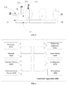
- an electronic apparatus 4000 comprising any of the display apparatus provided in the first embodiment.
- the electronic apparatus 4000 may be a desktop computer, a notebook computer, a mobile phone, a tablet and a PDA, and may also be a smart wearable device such as a sports bracelet and a sports watch.
- the electronic apparatus 4000 may comprise a processor 4010 , a memory 4020 , an interface device 4030 , a communication device 4040 , a display apparatus 4050 , an input device 4060 , a loudspeaker 4070 , a microphone 4080 , and so on.
- the processor 4010 may be a central processing unit CPU, a microprocessing unit MCU and so on.
- the memory 4020 comprises for example a ROM (read-only memory), a RAM (random access memory), a nonvolatile memory such as a hard disk and so on.
- the interface device 4030 comprises for example a USB interface, an earphone interface and so on.
- the communication device 4040 is capable of for example wired or wireless communication.
- the display apparatus 4050 is any of the display apparatus provided in the first embodiment.
- the input device 4060 may comprise for example a touch screen, a keyboard and so on. A user may input/output voice information by using the loudspeaker 4070 and the microphone 4080 .
- the configuration of electronic apparatus 4000 shown in FIG. 4 is merely explanatory, and is not intended to limit the present disclosure and its application or use.
- the memory 4020 of the electronic apparatus 4000 is used to store instructions, and the instructions are used to control the processor 4010 to operate to execute any of the methods for treating failure of a light-emitting unit provided in the following third embodiment.
- FIG. 4 shows a plurality of devices of the electronic apparatus 4000 , the present disclosure may merely involve part of the devices of them; for example, the electronic apparatus 4000 merely involves the processor 4010 , the memory 4020 and the display apparatus 4050 .
- a person skilled in the art can design the instructions according to the solution disclosed by the present disclosure. How the instructions control the processor to operate is well known in the art, and is not described in detail here.
- the present embodiment further provides a method for treating failure of a light-emitting unit, applied to any of the display apparatus provided in the first embodiment, which is not discussed here further.
- the method for treating failure of a light-emitting unit as shown in FIG. 5 , comprises:
- Step S 5100 when it is determined that a first light-emitting unit of the display apparatus has failed, inflating a high-refractive-index gas into at least one of side walls of a first light-transmitting unit provided corresponding to the first light-emitting unit to configure the light refraction passageway of the side walls, so that a light emitted by a second light-emitting unit that neighbors the first light-emitting unit and normally emits light passes through the light refraction passageway, is refracted, and emits out from an area corresponding to the first light-emitting unit in a direction perpendicular to the first light-emitting unit.
- the light-emitting device in the display apparatus comprises a plurality of light-emitting units that form a matrix arrangement.
- each of the light-emitting units can normally emit light.
- a light-emitting unit has failed, it appears abnormal light emitting or insufficient light output amount.
- the light refraction passageway of the side walls can be configured, so that a light emitted by a second light-emitting unit that neighbors the first light-emitting unit and normally emits light passes through the light refraction passageway, is refracted, and emits out from an area corresponding to the first light-emitting unit in a direction perpendicular to the first light-emitting unit, to compensate for the light output amount of the first light-emitting unit.
- a high-refractive-index gas such as an inert gas
- all of the four side walls of the shown light-emitting unit are a trapezoid gas tank.
- the four side walls of the light-emitting unit may be filled with an inert gas, wherein the inert gas may be sealedly stored in the display apparatus.
- the trapezoid gas tank is provided with at least one inflating opening that can be controlled to open and close, and when the first light-emitting unit is compensated for the light output amount, the inflating opening is controlled to open, or, the inert gas may flow into the gas tank after flowing into an inlet of the display apparatus that communicates with the exterior. After the inert gas is put into the four side walls of the first light-emitting unit ( FIG.
- the lights emitted by eight second light-emitting units around the first light-emitting unit can pass through the light refraction passageway of the corresponding side walls, so that a light emitted by a second light-emitting unit that neighbors the first light-emitting unit and normally emits light passes through the light refraction passageway, is refracted, and emits out from an area corresponding to the first light-emitting unit in a direction perpendicular to the first light-emitting unit, to more efficiently compensate for the light output amount of the first light-emitting unit.
- the light output amount of each of the light-emitting units can be obtained by driving the light-emitting devices of the display apparatus to emit light, and then photographing an image of the display apparatus by using for example an external high-resolution camera and processing.
- the light-emitting units are OLED pixel dots
- the brightness values of the OLED pixel dots can be obtained.
- the method for treating failure of a light-emitting unit of the present embodiment further comprises a step of determining the failure of the first light-emitting unit by acquiring light output amount of each of the light-emitting units of the display apparatus.
- Step S 5200 After Step S 5100 starts to compensate for the light output amount of the first light-emitting unit, the process enters Step S 5200 , which is, when it is detected that a light output amount of the first light-emitting unit reaches a normal threshold, stopping inflating the high-refractive-index gas into the side walls, wherein the normal threshold is determined according to a light output amount of the second light-emitting unit.
- the normal threshold is determined according to a light output amount of the second light-emitting unit.
- the normal threshold may be the weighted average of the light output amounts of the second light-emitting units that are involved in the compensating for the light output amount of the first light-emitting unit.
- all of the four side walls of the first light-emitting unit are filled with an inert gas, so that the lights emitted by eight second light-emitting units around the first light-emitting unit are refracted by the side walls of the first light-emitting unit to compensate for the light output amount of the first light-emitting unit.
- the normal threshold X th is calculated according to the formula 1:
- the light output amount (or brightness value) of each of the light-emitting units may be obtained in the process of implementing Step S 5100 by in real time monitoring and photographing by using an external high-resolution camera to acquire the light output amount of the display apparatus, for example acquiring the images of the display apparatus with a proper frequency (interval period), and using an image processing method.
- the inflating the high-refractive-index gas into the side walls of the first light-emitting unit may be stopped.
- the above method for treating failure of a light-emitting unit provided in the present embodiment can, when a light-emitting unit of the display apparatus provided in the first embodiment has failed, put a high-refractive-index gas into the side walls of the light-transmitting unit corresponding to the failed light-emitting unit, so that the lights emitted by the normal light-emitting units around the failed light-emitting unit are refracted by the side walls, and emit out from the area corresponding to the failed light-emitting unit, to compensate for the light output amount of the failed light-emitting unit, to realize the repairing on the failed light-emitting unit.
- the present disclosure does not need to dismantle the display apparatus, and has simple and convenient operation.
- the present disclosure can effectively improve the production yield of the display apparatus.
- the repairing is simple and low cost, which improves the user experience.
- the present disclosure is particularly applicable to failed OLED pixel dots when the display apparatus is an OLED screen.
- an apparatus 7000 for treating failure of a light-emitting unit comprising a light-emitting compensating unit 700 and a compensation controlling unit 7200 , and in some embodiments, further comprising a failure determining unit 7300 , for implementing the method for treating failure of a light-emitting unit provided in the present embodiment, which is not discussed here further.
- the apparatus 7000 for treating failure of a light-emitting unit comprises:
- a light-emitting compensating unit 7100 for, when it is determined that a first light-emitting unit of the display apparatus has failed, inflating a high-refractive-index gas into at least one of side walls of a first light-transmitting unit provided corresponding to the first light-emitting unit to configure the light refraction passageway of the side walls, so that a light emitted by a second light-emitting unit that neighbors the first light-emitting unit and normally emits light passes through the light refraction passageway, is refracted, and emits out from an area corresponding to the first light-emitting unit in a direction perpendicular to the first light-emitting unit; and
- a compensation controlling unit 7200 for, when it is detected that a light output amount of the first light-emitting unit reaches a normal threshold, stopping inflating the high-refractive-index gas into the side walls, wherein the normal threshold is determined according to a light output amount of the second light-emitting unit.
- the display apparatus sealedly stores a high-refractive-index gas
- each of the side walls of the light-transmitting unit is a gas tank that has at least one inflating opening, and the inflating opening can be controlled to open or close.
- the light-emitting compensating unit 7100 may be a solenoid valve controlling circuit that can cause the high-refractive-index gas, for example an inert gas, sealedly stored in the display apparatus to be put into the gas tank, wherein the solenoid valve controlling circuit may be built in the display apparatus.
- the compensation controlling unit 7200 may be a microprocessing unit MCU, and when it is detected that the light output amount of the first light-emitting unit reaches a normal threshold, controls the inflating opening to close, to stop inflating the high-refractive-index gas into the side walls.
- the apparatus 7000 for treating failure of a light-emitting unit may further comprise a failure determining unit 7300 , for determining the failure of the first light-emitting unit by acquiring light output amount of each of the light-emitting units of the display apparatus.
- the failure determining unit 7300 may be implemented together by part or all of the functional modules of the microprocessing unit MCU and the high-resolution camera that has an interface with the microprocessing unit MCU and is external to the display apparatus.
- the embodiments of the present disclosure have been described above by referring to the drawings.
- the method and apparatus provided by the present embodiment can, when a light-emitting unit of the display apparatus provided in the first embodiment has failed, put a high-refractive-index gas into the side walls of the light-transmitting unit corresponding to the failed light-emitting unit, so that the lights emitted by the normal light-emitting units around the failed light-emitting unit are refracted by the side walls, and emit out from the area corresponding to the failed light-emitting unit, to compensate for the light output amount of the failed light-emitting unit, to realize the repairing on the failed light-emitting unit.
- the present disclosure does not need to dismantle the display apparatus, and has simple and convenient operation.
- the present disclosure can effectively improve the production yield of the display apparatus.
- the repairing is simple and low cost, which can effectively improve the user experience.
- the present disclosure is particularly applicable to failed OLED pixel dots when the display apparatus is an OLED screen.
- the apparatus 7000 for treating failure of a light-emitting unit may be implemented by various modes.
- the apparatus 7000 for treating failure of a light-emitting unit may be implemented by configuring a processor by using instructions.
- the instructions are stored in an ROM, and when the apparatus is started up, the instructions are read from the ROM to a programmable device to implement the apparatus 7000 for treating failure of a light-emitting unit.
- the apparatus 7000 for treating failure of a light-emitting unit may be incorporated into a dedicated device (for example an ASIC).
- the apparatus 7000 for treating failure of a light-emitting unit may be implemented by being separated into mutually independent units, or be implemented integratedly.
- the apparatus 7000 for treating failure of a light-emitting unit may be implemented by using one of the above implementing modes, or may be implemented by using the combination of two or more of the above implementing modes.
- the present disclosure may be implemented as a system, a method and/or a computer program product.
- the computer program product may comprise a computer readable storage medium having a computer readable program instruction thereon for causing a processor to carry out the aspects of the present disclosure.
- the computer readable storage medium may be a tangible device that can retain and store an instruction for use by an instruction execution device.
- the computer readable storage medium may be, for example, but is not limited to, an electronic storage device, a magnetic storage device, an optical storage device, an electromagnetic storage device, a semiconductor storage device, or any suitable combination thereof.
- a non-exhaustive list of more specific examples of the computer readable storage medium includes: a portable computer diskette, a hard disk, a random access memory (RAM), a read-only memory (ROM), an erasable programmable read-only memory (EPROM or flash memory), a static random access memory (SRAM), a portable compact disc read-only memory (CD-ROM), a digital versatile disk (DVD), a memory stick, a floppy disk, a mechanically encoded device such as punch-cards or raised structures in a groove having an instruction recorded thereon, and any suitable combination thereof.
- RAM random access memory
- ROM read-only memory
- EPROM or flash memory erasable programmable read-only memory
- SRAM static random access memory
- CD-ROM compact disc read-only memory
- DVD digital versatile disk
- memory stick a floppy disk
- mechanically encoded device such as punch-cards or raised structures in a groove having an instruction recorded thereon, and any suitable combination thereof.
- a computer readable storage medium is not to be construed as being a transitory signal per se, such as a radio wave or other freely propagating electromagnetic waves, an electromagnetic wave propagating through a waveguide or other transmission media (for example, a light pulse passing through a fiber-optic cable), or an electrical signal transmitted through a wire.
- the computer readable program instruction described herein may be downloaded to respective computing/processing devices from a computer readable storage medium or to an external computer or external storage device via a network, for example, the Internet, a local area network, a wide area network and/or a wireless network.
- the network may comprise copper transmission cables, optical fiber transmission, wireless transmission, routers, firewalls, switches, gateway computers and/or edge servers.
- a network adapter card or network interface in each computing/processing device receives the computer readable program instructions from the network and forwards the computer readable program instructions for storage in a computer readable storage medium within the respective computing/processing device.
- the computer readable program instructions for carrying out the operations of the present disclosure may be assembler instructions, instruction-set-architecture (ISA) instructions, machine instructions, machine dependent instructions, microcode, firmware instructions, state-setting data, or either source code or object code written in any combination of one or more programming languages, including an object oriented programming language such as Smalltalk, C++ or the like, and conventional procedural programming languages, such as the “C” programming language or similar programming languages.
- the computer readable program instructions may execute entirely on the user's computer, partly on the user's computer, as a stand-alone software package, partly on the user's computer and partly on a remote computer, or entirely on a remote computer or server.
- the remote computer may be connected to the user's computer through any type of network, including a local area network (LAN) or a wide area network (WAN), or the connection may be made to an external computer (for example, through the Internet using an Internet Service Provider).
- electronic circuitry including, for example, programmable logic circuitry, field-programmable gate arrays (FPGA), or programmable logic arrays (PLA) may execute the computer readable program instructions by utilizing state information of the computer readable program instructions to personalize the electronic circuitry, in order to perform the aspects of the present disclosure.
- These computer readable program instructions may be provided to a processor of a general purpose computer, special purpose computer, or other programmable data processing device to produce a machine, such that the instructions, which execute via the processor of the computer or other programmable data processing device, create a means for implementing the functions/acts specified in the flowchart and/or block diagram block or blocks.
- These computer readable program instructions may also be stored in a computer readable storage medium that can direct a computer, a programmable data processing device, and/or other devices to function in a particular manner, such that the computer readable storage medium having instructions stored therein comprises an article of manufacture including instructions which implement the aspects of the functions/acts specified in the flowchart and/or block diagram block or blocks.
- the computer readable program instructions may also be loaded onto a computer, other programmable data processing device, or other device to cause a series of operational steps to be performed on the computer, other programmable data processing device, or other device to produce a computer implemented process, such that the instructions which execute on the computer, the other programmable data processing device, or the other device implement the functions/acts specified in the flowchart and/or block diagram block or blocks.
- each block in the flow chart or block diagram may represent a module, a program segment, or a portion of the instruction.
- the module, the program segment or the portion of the instruction includes one or more executable instructions for implementing specified logic functions.
- the function indicated in the block may also occur in an order different from the one represented in the drawings. For example, two consecutive blocks actually may be executed substantially in parallel, and sometimes they may also be executed in a reverse order, depending on the involved functions.
- each block in the block diagram and/or flow chart, and any combinations of the blocks in the block diagram and/or flow chart may be implemented by a dedicated hardware-based system for implementing specified functions or actions, or a combination of the dedicated hardware and the computer instructions. It is well known to those skilled in the art that the implementation by hardware, the implementation by software, and the implementation by a combination of software and hardware are equivalent.
Landscapes
- Engineering & Computer Science (AREA)
- Physics & Mathematics (AREA)
- General Physics & Mathematics (AREA)
- Theoretical Computer Science (AREA)
- Microelectronics & Electronic Packaging (AREA)
- Manufacturing & Machinery (AREA)
- Optics & Photonics (AREA)
- Electroluminescent Light Sources (AREA)
- Devices For Indicating Variable Information By Combining Individual Elements (AREA)
Abstract
Description
wherein αi are the corresponding weighting coefficients, and may be acquired according to the experience in engineering, and in an example, αi=1 (i=1, . . . , 8).
Claims (12)
Applications Claiming Priority (4)
| Application Number | Priority Date | Filing Date | Title |
|---|---|---|---|
| CN201610847791.0 | 2016-09-23 | ||
| CN201610847791.0A CN106328010B (en) | 2016-09-23 | 2016-09-23 | Show equipment, electronic equipment, luminescence unit break treat with method and apparatus |
| CN201610847791 | 2016-09-23 | ||
| PCT/CN2016/114001 WO2018053972A1 (en) | 2016-09-23 | 2016-12-31 | Display device, electronic device, and light emitting unit damage processing method and device |
Publications (2)
| Publication Number | Publication Date |
|---|---|
| US20190189716A1 US20190189716A1 (en) | 2019-06-20 |
| US10615232B2 true US10615232B2 (en) | 2020-04-07 |
Family
ID=57820572
Family Applications (1)
| Application Number | Title | Priority Date | Filing Date |
|---|---|---|---|
| US16/322,013 Active US10615232B2 (en) | 2016-09-23 | 2016-12-31 | Display device, electronic device, and light emitting unit damage processing method and device |
Country Status (3)
| Country | Link |
|---|---|
| US (1) | US10615232B2 (en) |
| CN (1) | CN106328010B (en) |
| WO (1) | WO2018053972A1 (en) |
Citations (12)
| Publication number | Priority date | Publication date | Assignee | Title |
|---|---|---|---|---|
| CN1099150A (en) | 1993-04-30 | 1995-02-22 | 夏普公司 | Liquid crystal indicator reaches the method for defect correcting therein |
| JP2003045652A (en) | 2001-07-30 | 2003-02-14 | Matsushita Electric Ind Co Ltd | OLED display |
| JP2003051383A (en) | 2001-08-07 | 2003-02-21 | Matsushita Electric Ind Co Ltd | OLED display |
| CN101994930A (en) | 2009-08-14 | 2011-03-30 | 连营科技股份有限公司 | Light emitting diode device with compensation mechanism |
| US20110130981A1 (en) | 2009-11-30 | 2011-06-02 | Ignis Innovation Inc. | System and methods for aging compensation in amoled displays |
| CN102749740A (en) | 2012-07-27 | 2012-10-24 | 南京中电熊猫液晶显示科技有限公司 | Method for optically repairing point defect |
| CN104217684A (en) | 2014-09-11 | 2014-12-17 | 西安诺瓦电子科技有限公司 | LED (light emitting diode) defective point processing method and detection method and LED display control method |
| CN104659055A (en) | 2013-11-25 | 2015-05-27 | 乐金显示有限公司 | Organic electroluminescent device and repairing method |
| CN205092244U (en) | 2015-08-07 | 2016-03-16 | 信利半导体有限公司 | OLED display and electronic equipment |
| US20160126501A1 (en) | 2014-10-31 | 2016-05-05 | Lg Display Co., Ltd. | Organic light emitting display device |
| CN105611196A (en) | 2015-12-18 | 2016-05-25 | 广东欧珀移动通信有限公司 | Image defective pixel compensation method and device and terminal device |
| US20160189593A1 (en) | 2014-12-29 | 2016-06-30 | Lg Display Co., Ltd. | Organic light emitting display device and repair method thereof |
-
2016
- 2016-09-23 CN CN201610847791.0A patent/CN106328010B/en active Active
- 2016-12-31 US US16/322,013 patent/US10615232B2/en active Active
- 2016-12-31 WO PCT/CN2016/114001 patent/WO2018053972A1/en not_active Ceased
Patent Citations (15)
| Publication number | Priority date | Publication date | Assignee | Title |
|---|---|---|---|---|
| CN1099150A (en) | 1993-04-30 | 1995-02-22 | 夏普公司 | Liquid crystal indicator reaches the method for defect correcting therein |
| JP2003045652A (en) | 2001-07-30 | 2003-02-14 | Matsushita Electric Ind Co Ltd | OLED display |
| JP2003051383A (en) | 2001-08-07 | 2003-02-21 | Matsushita Electric Ind Co Ltd | OLED display |
| CN101994930A (en) | 2009-08-14 | 2011-03-30 | 连营科技股份有限公司 | Light emitting diode device with compensation mechanism |
| US20110130981A1 (en) | 2009-11-30 | 2011-06-02 | Ignis Innovation Inc. | System and methods for aging compensation in amoled displays |
| CN102725786A (en) | 2009-11-30 | 2012-10-10 | 伊格尼斯创新公司 | System and methods for aging compensation in AMOLED displays |
| CN102749740A (en) | 2012-07-27 | 2012-10-24 | 南京中电熊猫液晶显示科技有限公司 | Method for optically repairing point defect |
| CN104659055A (en) | 2013-11-25 | 2015-05-27 | 乐金显示有限公司 | Organic electroluminescent device and repairing method |
| US20170033168A1 (en) | 2013-11-25 | 2017-02-02 | Lg Display Co., Ltd. | Organic electroluminescent device and repairing method thereof |
| CN104217684A (en) | 2014-09-11 | 2014-12-17 | 西安诺瓦电子科技有限公司 | LED (light emitting diode) defective point processing method and detection method and LED display control method |
| US20160126501A1 (en) | 2014-10-31 | 2016-05-05 | Lg Display Co., Ltd. | Organic light emitting display device |
| US20160189593A1 (en) | 2014-12-29 | 2016-06-30 | Lg Display Co., Ltd. | Organic light emitting display device and repair method thereof |
| CN105741734A (en) | 2014-12-29 | 2016-07-06 | 乐金显示有限公司 | Organic Light Emitting Display Device And Repair Method Thereof |
| CN205092244U (en) | 2015-08-07 | 2016-03-16 | 信利半导体有限公司 | OLED display and electronic equipment |
| CN105611196A (en) | 2015-12-18 | 2016-05-25 | 广东欧珀移动通信有限公司 | Image defective pixel compensation method and device and terminal device |
Non-Patent Citations (2)
| Title |
|---|
| International Bureau of WIPO, International Search Report and Written Opinion in Application No. PCT/CN2016/114001, dated Jul. 10, 2019. |
| National Intellectual Property Administration of the Peoples Republic of China, First Office Action in Application No. 2018073002009870, dated Aug. 2, 2018. |
Also Published As
| Publication number | Publication date |
|---|---|
| CN106328010A (en) | 2017-01-11 |
| US20190189716A1 (en) | 2019-06-20 |
| CN106328010B (en) | 2019-01-04 |
| WO2018053972A1 (en) | 2018-03-29 |
Similar Documents
| Publication | Publication Date | Title |
|---|---|---|
| CN105913787B (en) | The detection method and display module and electronic equipment of substandard state | |
| EP3792906A1 (en) | Method, apparatus, and device for adjusting display brightness, display device, and storage medium | |
| US11250798B2 (en) | Timing controller, liquid crystal display apparatus and display driving method | |
| US20160170702A1 (en) | Devices and methods of image-splitting for dual-layer high dynamic range displays | |
| US20190156746A1 (en) | Electronic device and operation control method of electronic device | |
| EP3026708A1 (en) | Organic light-emitting diode array substrate and manufacturing method thereof, and display device | |
| US10360830B2 (en) | GIP circuit and driving method therefor, and flat panel display device | |
| CN106033656A (en) | display device | |
| US11764195B2 (en) | Display panel having a plurality of display regions overlap | |
| WO2019176085A1 (en) | Display device | |
| WO2017000450A1 (en) | Display drive method, display panel and manufacturing method therefor, and display device | |
| US9454925B1 (en) | Image degradation reduction | |
| US9799574B2 (en) | Gate integrated driving circuit and a restoring method thereof, a display panel and a display apparatus | |
| CN113870802A (en) | Display device, control method thereof and related equipment | |
| JP2015505417A (en) | Light guide having an at least partially opaque coating on the ledge area | |
| US20160322002A1 (en) | Electronic paper display device and manufacturing method thereof | |
| US20180341856A1 (en) | Balancing memory consumption of multiple graphics processing units in deep learning | |
| JP2009229707A (en) | Liquid crystal display device | |
| US20210193770A1 (en) | Display substrate, display panel, display device and method for manufacturing display substrate | |
| US10615232B2 (en) | Display device, electronic device, and light emitting unit damage processing method and device | |
| CN105045371A (en) | Electronic device and information processing method | |
| CN117496899A (en) | Brightness adjustment method and device of near-eye optical system and near-eye optical system | |
| US20230135676A1 (en) | Touch device and driving method thereof | |
| KR102725786B1 (en) | Electronic device including display and operation method thereof | |
| US12505022B2 (en) | System testing method, electronic device, and computer program product |
Legal Events
| Date | Code | Title | Description |
|---|---|---|---|
| AS | Assignment |
Owner name: GOERTEK TECHNOLOGY CO., LTD., CHINA Free format text: ASSIGNMENT OF ASSIGNORS INTEREST;ASSIGNORS:LIU, XUN;TANG, MAOQING;REEL/FRAME:048192/0508 Effective date: 20190103 |
|
| FEPP | Fee payment procedure |
Free format text: ENTITY STATUS SET TO UNDISCOUNTED (ORIGINAL EVENT CODE: BIG.); ENTITY STATUS OF PATENT OWNER: LARGE ENTITY |
|
| STPP | Information on status: patent application and granting procedure in general |
Free format text: DOCKETED NEW CASE - READY FOR EXAMINATION |
|
| STPP | Information on status: patent application and granting procedure in general |
Free format text: NOTICE OF ALLOWANCE MAILED -- APPLICATION RECEIVED IN OFFICE OF PUBLICATIONS |
|
| STPP | Information on status: patent application and granting procedure in general |
Free format text: AWAITING TC RESP., ISSUE FEE NOT PAID |
|
| STPP | Information on status: patent application and granting procedure in general |
Free format text: NOTICE OF ALLOWANCE MAILED -- APPLICATION RECEIVED IN OFFICE OF PUBLICATIONS |
|
| STPP | Information on status: patent application and granting procedure in general |
Free format text: PUBLICATIONS -- ISSUE FEE PAYMENT RECEIVED |
|
| STCF | Information on status: patent grant |
Free format text: PATENTED CASE |
|
| MAFP | Maintenance fee payment |
Free format text: PAYMENT OF MAINTENANCE FEE, 4TH YEAR, LARGE ENTITY (ORIGINAL EVENT CODE: M1551); ENTITY STATUS OF PATENT OWNER: LARGE ENTITY Year of fee payment: 4 |