US10600985B2 - Organic electroluminescence display apparatus - Google Patents
Organic electroluminescence display apparatus Download PDFInfo
- Publication number
- US10600985B2 US10600985B2 US15/839,652 US201715839652A US10600985B2 US 10600985 B2 US10600985 B2 US 10600985B2 US 201715839652 A US201715839652 A US 201715839652A US 10600985 B2 US10600985 B2 US 10600985B2
- Authority
- US
- United States
- Prior art keywords
- shortest distance
- light
- light shielding
- shielding member
- organic electroluminescence
- Prior art date
- Legal status (The legal status is an assumption and is not a legal conclusion. Google has not performed a legal analysis and makes no representation as to the accuracy of the status listed.)
- Active, expires
Links
- 238000005401 electroluminescence Methods 0.000 title claims abstract description 75
- 239000010410 layer Substances 0.000 claims abstract description 154
- 239000012044 organic layer Substances 0.000 claims abstract description 38
- 238000006243 chemical reaction Methods 0.000 claims description 66
- 239000000758 substrate Substances 0.000 claims description 27
- 238000005538 encapsulation Methods 0.000 claims 2
- 239000010409 thin film Substances 0.000 description 33
- 101100214488 Solanum lycopersicum TFT2 gene Proteins 0.000 description 20
- 238000007789 sealing Methods 0.000 description 17
- 239000004065 semiconductor Substances 0.000 description 13
- 101100489584 Solanum lycopersicum TFT1 gene Proteins 0.000 description 12
- 239000003990 capacitor Substances 0.000 description 12
- 239000000463 material Substances 0.000 description 10
- 101100440271 Caenorhabditis elegans ccf-1 gene Proteins 0.000 description 8
- 239000011229 interlayer Substances 0.000 description 8
- 102100027126 Echinoderm microtubule-associated protein-like 2 Human genes 0.000 description 7
- 101001057942 Homo sapiens Echinoderm microtubule-associated protein-like 2 Proteins 0.000 description 7
- 230000007423 decrease Effects 0.000 description 4
- 239000011810 insulating material Substances 0.000 description 4
- 239000005022 packaging material Substances 0.000 description 4
- 239000000049 pigment Substances 0.000 description 4
- 230000001681 protective effect Effects 0.000 description 4
- 102100024954 5-hydroxytryptamine receptor 3A Human genes 0.000 description 3
- 102100033210 CUGBP Elav-like family member 2 Human genes 0.000 description 3
- 101150051255 ETR3 gene Proteins 0.000 description 3
- 102100027094 Echinoderm microtubule-associated protein-like 1 Human genes 0.000 description 3
- 102100027095 Echinoderm microtubule-associated protein-like 3 Human genes 0.000 description 3
- 102100039327 Enoyl-[acyl-carrier-protein] reductase, mitochondrial Human genes 0.000 description 3
- 101150017422 HTR1 gene Proteins 0.000 description 3
- 101000761343 Homo sapiens 5-hydroxytryptamine receptor 3A Proteins 0.000 description 3
- 101001057941 Homo sapiens Echinoderm microtubule-associated protein-like 1 Proteins 0.000 description 3
- 101001057939 Homo sapiens Echinoderm microtubule-associated protein-like 3 Proteins 0.000 description 3
- 101000961707 Homo sapiens Enoyl-[acyl-carrier-protein] reductase, mitochondrial Proteins 0.000 description 3
- 101000653469 Homo sapiens T-complex protein 1 subunit zeta Proteins 0.000 description 3
- 101100024116 Saccharomyces cerevisiae (strain ATCC 204508 / S288c) MPT5 gene Proteins 0.000 description 3
- 101150051027 celf2 gene Proteins 0.000 description 3
- 239000011159 matrix material Substances 0.000 description 3
- 239000002952 polymeric resin Substances 0.000 description 3
- 230000027756 respiratory electron transport chain Effects 0.000 description 3
- 229920003002 synthetic resin Polymers 0.000 description 3
- 239000004642 Polyimide Substances 0.000 description 2
- VYPSYNLAJGMNEJ-UHFFFAOYSA-N Silicium dioxide Chemical compound O=[Si]=O VYPSYNLAJGMNEJ-UHFFFAOYSA-N 0.000 description 2
- XLOMVQKBTHCTTD-UHFFFAOYSA-N Zinc monoxide Chemical compound [Zn]=O XLOMVQKBTHCTTD-UHFFFAOYSA-N 0.000 description 2
- 229910052782 aluminium Inorganic materials 0.000 description 2
- 150000001875 compounds Chemical class 0.000 description 2
- 238000010586 diagram Methods 0.000 description 2
- 239000002019 doping agent Substances 0.000 description 2
- AMGQUBHHOARCQH-UHFFFAOYSA-N indium;oxotin Chemical compound [In].[Sn]=O AMGQUBHHOARCQH-UHFFFAOYSA-N 0.000 description 2
- 229910052749 magnesium Inorganic materials 0.000 description 2
- 239000000203 mixture Substances 0.000 description 2
- 229920000139 polyethylene terephthalate Polymers 0.000 description 2
- 239000005020 polyethylene terephthalate Substances 0.000 description 2
- 229920001721 polyimide Polymers 0.000 description 2
- -1 region Substances 0.000 description 2
- 229920005989 resin Polymers 0.000 description 2
- 239000011347 resin Substances 0.000 description 2
- 229910052814 silicon oxide Inorganic materials 0.000 description 2
- 229910052709 silver Inorganic materials 0.000 description 2
- YVTHLONGBIQYBO-UHFFFAOYSA-N zinc indium(3+) oxygen(2-) Chemical compound [O--].[Zn++].[In+3] YVTHLONGBIQYBO-UHFFFAOYSA-N 0.000 description 2
- TYHJXGDMRRJCRY-UHFFFAOYSA-N zinc indium(3+) oxygen(2-) tin(4+) Chemical compound [O-2].[Zn+2].[Sn+4].[In+3] TYHJXGDMRRJCRY-UHFFFAOYSA-N 0.000 description 2
- 102100036321 5-hydroxytryptamine receptor 2A Human genes 0.000 description 1
- 108091006146 Channels Proteins 0.000 description 1
- 101150068804 ETR2 gene Proteins 0.000 description 1
- 101000783617 Homo sapiens 5-hydroxytryptamine receptor 2A Proteins 0.000 description 1
- 229910052779 Neodymium Inorganic materials 0.000 description 1
- 239000004695 Polyether sulfone Substances 0.000 description 1
- 229910052581 Si3N4 Inorganic materials 0.000 description 1
- 229910004205 SiNX Inorganic materials 0.000 description 1
- XUIMIQQOPSSXEZ-UHFFFAOYSA-N Silicon Chemical compound [Si] XUIMIQQOPSSXEZ-UHFFFAOYSA-N 0.000 description 1
- 239000011358 absorbing material Substances 0.000 description 1
- 229910052791 calcium Inorganic materials 0.000 description 1
- 239000006229 carbon black Substances 0.000 description 1
- 229910052804 chromium Inorganic materials 0.000 description 1
- 229910052802 copper Inorganic materials 0.000 description 1
- 238000000605 extraction Methods 0.000 description 1
- 239000011521 glass Substances 0.000 description 1
- 229910052737 gold Inorganic materials 0.000 description 1
- 239000012535 impurity Substances 0.000 description 1
- 229910010272 inorganic material Inorganic materials 0.000 description 1
- 239000011147 inorganic material Substances 0.000 description 1
- 229910052741 iridium Inorganic materials 0.000 description 1
- 229910052744 lithium Inorganic materials 0.000 description 1
- PQXKHYXIUOZZFA-UHFFFAOYSA-M lithium fluoride Inorganic materials [Li+].[F-] PQXKHYXIUOZZFA-UHFFFAOYSA-M 0.000 description 1
- 229910001092 metal group alloy Inorganic materials 0.000 description 1
- 229910044991 metal oxide Inorganic materials 0.000 description 1
- 150000004706 metal oxides Chemical class 0.000 description 1
- 238000000034 method Methods 0.000 description 1
- 238000012986 modification Methods 0.000 description 1
- 230000004048 modification Effects 0.000 description 1
- 229910052750 molybdenum Inorganic materials 0.000 description 1
- 229910052759 nickel Inorganic materials 0.000 description 1
- 229910052763 palladium Inorganic materials 0.000 description 1
- 239000004033 plastic Substances 0.000 description 1
- 229920003023 plastic Polymers 0.000 description 1
- 229910052697 platinum Inorganic materials 0.000 description 1
- 229920000058 polyacrylate Polymers 0.000 description 1
- 229920006393 polyether sulfone Polymers 0.000 description 1
- 239000011112 polyethylene naphthalate Substances 0.000 description 1
- 239000011241 protective layer Substances 0.000 description 1
- 229910052710 silicon Inorganic materials 0.000 description 1
- 239000010703 silicon Substances 0.000 description 1
- HQVNEWCFYHHQES-UHFFFAOYSA-N silicon nitride Chemical compound N12[Si]34N5[Si]62N3[Si]51N64 HQVNEWCFYHHQES-UHFFFAOYSA-N 0.000 description 1
- 229910052719 titanium Inorganic materials 0.000 description 1
- 238000004078 waterproofing Methods 0.000 description 1
Images


Classifications
-
- H—ELECTRICITY
- H10—SEMICONDUCTOR DEVICES; ELECTRIC SOLID-STATE DEVICES NOT OTHERWISE PROVIDED FOR
- H10K—ORGANIC ELECTRIC SOLID-STATE DEVICES
- H10K59/00—Integrated devices, or assemblies of multiple devices, comprising at least one organic light-emitting element covered by group H10K50/00
- H10K59/10—OLED displays
- H10K59/12—Active-matrix OLED [AMOLED] displays
- H10K59/122—Pixel-defining structures or layers, e.g. banks
-
- H01L51/5203—
-
- H—ELECTRICITY
- H10—SEMICONDUCTOR DEVICES; ELECTRIC SOLID-STATE DEVICES NOT OTHERWISE PROVIDED FOR
- H10K—ORGANIC ELECTRIC SOLID-STATE DEVICES
- H10K59/00—Integrated devices, or assemblies of multiple devices, comprising at least one organic light-emitting element covered by group H10K50/00
- H10K59/10—OLED displays
- H10K59/12—Active-matrix OLED [AMOLED] displays
- H10K59/126—Shielding, e.g. light-blocking means over the TFTs
-
- H01L27/3246—
-
- H01L27/3258—
-
- H01L51/5036—
-
- H01L51/524—
-
- H01L51/5284—
-
- H—ELECTRICITY
- H10—SEMICONDUCTOR DEVICES; ELECTRIC SOLID-STATE DEVICES NOT OTHERWISE PROVIDED FOR
- H10K—ORGANIC ELECTRIC SOLID-STATE DEVICES
- H10K50/00—Organic light-emitting devices
- H10K50/10—OLEDs or polymer light-emitting diodes [PLED]
- H10K50/11—OLEDs or polymer light-emitting diodes [PLED] characterised by the electroluminescent [EL] layers
- H10K50/125—OLEDs or polymer light-emitting diodes [PLED] characterised by the electroluminescent [EL] layers specially adapted for multicolour light emission, e.g. for emitting white light
-
- H—ELECTRICITY
- H10—SEMICONDUCTOR DEVICES; ELECTRIC SOLID-STATE DEVICES NOT OTHERWISE PROVIDED FOR
- H10K—ORGANIC ELECTRIC SOLID-STATE DEVICES
- H10K50/00—Organic light-emitting devices
- H10K50/80—Constructional details
- H10K50/805—Electrodes
-
- H—ELECTRICITY
- H10—SEMICONDUCTOR DEVICES; ELECTRIC SOLID-STATE DEVICES NOT OTHERWISE PROVIDED FOR
- H10K—ORGANIC ELECTRIC SOLID-STATE DEVICES
- H10K50/00—Organic light-emitting devices
- H10K50/80—Constructional details
- H10K50/84—Passivation; Containers; Encapsulations
- H10K50/841—Self-supporting sealing arrangements
-
- H—ELECTRICITY
- H10—SEMICONDUCTOR DEVICES; ELECTRIC SOLID-STATE DEVICES NOT OTHERWISE PROVIDED FOR
- H10K—ORGANIC ELECTRIC SOLID-STATE DEVICES
- H10K50/00—Organic light-emitting devices
- H10K50/80—Constructional details
- H10K50/86—Arrangements for improving contrast, e.g. preventing reflection of ambient light
- H10K50/865—Arrangements for improving contrast, e.g. preventing reflection of ambient light comprising light absorbing layers, e.g. light-blocking layers
-
- H—ELECTRICITY
- H10—SEMICONDUCTOR DEVICES; ELECTRIC SOLID-STATE DEVICES NOT OTHERWISE PROVIDED FOR
- H10K—ORGANIC ELECTRIC SOLID-STATE DEVICES
- H10K59/00—Integrated devices, or assemblies of multiple devices, comprising at least one organic light-emitting element covered by group H10K50/00
- H10K59/10—OLED displays
- H10K59/12—Active-matrix OLED [AMOLED] displays
- H10K59/124—Insulating layers formed between TFT elements and OLED elements
-
- H—ELECTRICITY
- H10—SEMICONDUCTOR DEVICES; ELECTRIC SOLID-STATE DEVICES NOT OTHERWISE PROVIDED FOR
- H10K—ORGANIC ELECTRIC SOLID-STATE DEVICES
- H10K59/00—Integrated devices, or assemblies of multiple devices, comprising at least one organic light-emitting element covered by group H10K50/00
- H10K59/10—OLED displays
- H10K59/12—Active-matrix OLED [AMOLED] displays
- H10K59/131—Interconnections, e.g. wiring lines or terminals
-
- H—ELECTRICITY
- H10—SEMICONDUCTOR DEVICES; ELECTRIC SOLID-STATE DEVICES NOT OTHERWISE PROVIDED FOR
- H10K—ORGANIC ELECTRIC SOLID-STATE DEVICES
- H10K59/00—Integrated devices, or assemblies of multiple devices, comprising at least one organic light-emitting element covered by group H10K50/00
- H10K59/30—Devices specially adapted for multicolour light emission
- H10K59/38—Devices specially adapted for multicolour light emission comprising colour filters or colour changing media [CCM]
-
- H—ELECTRICITY
- H10—SEMICONDUCTOR DEVICES; ELECTRIC SOLID-STATE DEVICES NOT OTHERWISE PROVIDED FOR
- H10K—ORGANIC ELECTRIC SOLID-STATE DEVICES
- H10K59/00—Integrated devices, or assemblies of multiple devices, comprising at least one organic light-emitting element covered by group H10K50/00
- H10K59/80—Constructional details
- H10K59/805—Electrodes
-
- H01L27/322—
-
- H—ELECTRICITY
- H10—SEMICONDUCTOR DEVICES; ELECTRIC SOLID-STATE DEVICES NOT OTHERWISE PROVIDED FOR
- H10K—ORGANIC ELECTRIC SOLID-STATE DEVICES
- H10K59/00—Integrated devices, or assemblies of multiple devices, comprising at least one organic light-emitting element covered by group H10K50/00
- H10K59/80—Constructional details
- H10K59/87—Passivation; Containers; Encapsulations
- H10K59/871—Self-supporting sealing arrangements
Definitions
- aspects of embodiments of the invention relate to an organic electroluminescence display apparatus.
- organic electroluminescence display apparatus Various display apparatuses used in multimedia apparatuses, such as televisions, portable phones, tablet computers, navigation systems, and game consoles have been developed, and a self-luminous organic electroluminescence display apparatus has been developed as one kind of these display apparatuses.
- the organic electroluminescence display apparatus holes provided from a first electrode are recombined with electrons provided from a second electrode in a light-emitting layer to emit light.
- the organic electroluminescence display apparatus displays an image using the emitted light.
- the organic electroluminescence display apparatus may have a structure in which an electrode and a light-emitting layer are stacked on an insulating layer referred to as a planarization layer.
- light emitted from the light-emitting layer may travel in parallel to a thickness direction of the organic electroluminescence display apparatus and may also be dispersed in both lateral directions.
- light efficiency of the organic electroluminescence display apparatus may be deteriorated, and lights of adjacent sub-pixels may be mixed with each other.
- an organic electroluminescence display apparatus has improved or increased light efficiency.
- an organic electroluminescence display apparatus includes: an insulating layer including a flat surface and a first concave surface and a second concave surface extending from one end and another end of the flat surface, respectively; a first electrode disposed on the insulating layer and including a first concave electrode surface overlapping with the first concave surface, a second concave electrode surface overlapping with the second concave surface, and a flat electrode surface overlapping with the flat surface; an organic layer disposed on the first electrode; a second electrode disposed on the organic layer; and a plurality of light shielding members disposed on the second electrode and disposed with an opening therebetween, the opening overlapping with the organic layer.
- a first shortest distance is defined from the one end of the light shielding member to a first boundary axis between the first concave surface and the flat surface
- a second shortest distance is defined from another end of the light shielding member adjacent to the first concave surface to the first boundary axis
- a third shortest distance is defined from the insulating layer to the light shielding member. The first shortest distance is greater than twice the third shortest distance.
- the second shortest distance may be shorter than the first shortest distance.
- the first shortest distance and the third shortest distance may satisfy the following Equation 1:
- the second shortest distance may be from 1 ⁇ m to 100 ⁇ m.
- a fourth shortest distance may be defined to correspond to a width of the opening, and a ratio of the second shortest distance to the fourth shortest distance may be greater than 0.005:1 and less than 0.5:1.
- a fifth shortest distance is defined from another end of the light shielding member adjacent to the second concave surface to a second boundary axis between the second concave surface and the flat surface
- a sixth shortest distance is defined from the one end of the light shielding member adjacent to the second concave surface to the second boundary axis. The sixth shortest distance is greater than twice the third shortest distance.
- the fifth shortest distance may be shorter than the sixth shortest distance.
- the organic electroluminescence display apparatus may further include a color conversion layer disposed on the second electrode and including an illuminant that absorbs first color light outputted from the organic layer and emits light having a color different from the first color light.
- the illuminant may include a first illuminant absorbing the first color light and emitting second color light, and a second illuminant absorbing the first color light and emitting third color light having a color different from the second color light.
- the color conversion layer may include a first conversion part including the first illuminant, a second conversion part including the second illuminant, and a third conversion part transmitting the first color light.
- the first, second, and third conversion parts may be spaced apart from each other in a plan view, and the light shielding members may be disposed between the first, second, and third conversion parts spaced apart from each other.
- the first color light may be blue light.
- the first concave surface and the second concave surface may be symmetrical with respect to the flat surface.
- the organic electroluminescence display apparatus may further include a pixel defining layer disposed on the insulating layer and exposing a portion of the first electrode overlapping with the organic layer.
- FIG. 1 is a perspective view illustrating an organic electroluminescence display apparatus according to one or more embodiments of the invention.
- FIG. 2 is a perspective view illustrating a display panel of the organic electroluminescence display apparatus of FIG. 1 .
- FIG. 3 is a circuit diagram illustrating an example of a pixel of the display panel of FIG. 2 .
- FIG. 4 is a partial plan view of the display panel illustrated in FIG. 2 .
- FIG. 5 is a partial cross-sectional view illustrating a display apparatus according to one or more embodiments of the invention.
- FIG. 6 illustrates conversion of light on the basis of first to third organic electroluminescence elements and first to third conversion parts of the display apparatus illustrated in FIG. 5 .
- FIG. 7 is an enlarged view of a region “AA” of FIG. 5 .
- FIG. 8 is a cross-sectional view illustrating the travel of light emitted from an organic light-emitting layer according to one or more embodiments of the invention.
- FIG. 9 is a graph illustrating a ratio of light transmitted from an organic light-emitting layer to a conversion part in accordance with a variation of a second shortest distance illustrated in FIG. 7 .
- FIG. 10 is a graph illustrating a light leakage ratio according to variations of a first shortest distance and a third shortest distance illustrated in FIG. 7 .
- first the terms “first,” “second,” etc. may be used herein to describe various elements, components, regions, layers, and/or sections, these elements, components, regions, layers, and/or sections should not be limited by these terms. Rather, these terms are used to distinguish one element, component, region, layer, or section from another element, component, region, layer, or section. Thus, a “first” element, component, region, layer, or section described below could be termed a “second” element, component, region, layer, or section without departing from the teachings herein.
- FIG. 1 is a perspective view illustrating an organic electroluminescence display apparatus according to one or more embodiments of the invention.
- FIG. 2 is a perspective view illustrating a display panel of the organic electroluminescence display apparatus of FIG. 1 .
- FIG. 3 is a circuit diagram illustrating an example of a pixel of the display panel of FIG. 2 .
- FIG. 4 is a partial plan view of the display panel illustrated in FIG. 2 .
- an organic electroluminescence display apparatus DD illustrated in FIG. 1 may be applied to a tablet personal computer, a smartphone, a personal digital assistant (PDA), a portable multimedia player (PMP), a game console, and a watch-type electronic device, for example.
- the organic electroluminescence display apparatus DD may also be applied to large-sized electronic devices (e.g., a television and/or an external billboard) and small and medium-sized electronic devices (e.g., a personal computer, a notebook computer, a car navigation unit, and/or a camera).
- the organic electroluminescence display apparatus DD may include a display panel DP and a protective member PM disposed on the display panel DP.
- the display panel DP may be an organic electroluminescence display panel.
- the protective member PM may be a support member supporting the display panel DP or a window member protecting the display panel DP.
- the display panel DP is parallel to a plane defined by a first direction DR 1 and a second direction DR 2 .
- a normal direction of the display panel DP is indicated by a third direction DR 3 .
- the third direction DR 3 also indicates a thickness direction of the organic electroluminescence display apparatus DD.
- a top surface (or a front surface) and a bottom surface (or a back surface) of each of the members are defined by the third direction DR 3 .
- the directions DR 1 , DR 2 , and DR 3 may be relative concepts and may be changed into other directions.
- the organic electroluminescence display apparatus DD is flat, as depicted in FIG. 1 .
- the organic electroluminescence display apparatus DD according to the invention may be realized as a flexible display apparatus.
- components e.g., the display panel DP and the protective member PM included in the organic electroluminescence display apparatus DD may include flexible materials and can be bent, expanded, or pressed.
- the display panel DP may include a display area DP-DA, on which an image is displayed, and a non-display area DP-NDA adjacent to the display area DP-DA when viewed in a plan view.
- the display area DP-DA and the non-display area DP-NDA may be changed depending on a structure and/or a design of the display panel DP.
- the display panel DP may include a plurality of pixels PX overlapping with the display area DP-DA.
- the pixels PX included in the display panel DP are shown to be arranged in a matrix form in FIG. 2 .
- the pixels PX may be arranged in a non-matrix form, e.g., a pentile form.
- the display panel DP may further include a plurality of gate lines and a plurality of data lines, which are connected to the plurality of pixels PX.
- each of the pixels PX receives a gate signal from a corresponding one of the gate lines and receives a data signal from a corresponding one of the data lines.
- Each of the pixels PX may be turned on in response to the corresponding gate signal and may generate light in response to the corresponding data signal to display an image.
- Each of the pixels PX includes at least one thin film transistor, at least one capacitor, and an organic electroluminescence element.
- FIG. 3 illustrates an equivalent circuit of a pixel PX ij connected to an i-th gate line SLi of the gate lines and a j-th data line DLj of the data lines.
- the pixel PX ij includes a switching thin film transistor TFT 1 , a driving thin film transistor TFT 2 , a capacitor Cap, and an organic electroluminescence element OEL ij .
- the switching thin film transistor TFT 1 includes a control electrode connected to the i-th gate line SLi, an input electrode connected to the j-th data line DLj, and an output electrode.
- the switching thin film transistor TFT 1 outputs the data signal, applied to the j-th data line DLj, in response to the gate signal applied to the i-th gate line SLi.
- the capacitor Cap includes a first capacitor electrode connected to the switching thin film transistor TFT 1 , and a second capacitor electrode receiving a first power source voltage ELVDD.
- the capacitor Cap is charged with charges corresponding to a difference between the first power source voltage ELVDD and a voltage corresponding to the data signal received from the switching thin film transistor TFT 1 .
- the driving thin film transistor TFT 2 includes a control electrode connected to the output electrode of the switching thin film transistor TFT 1 and the first capacitor electrode of the capacitor Cap, an input electrode receiving the first power source voltage ELVDD, and an output electrode.
- the output electrode of the driving thin film transistor TFT 2 is connected to the organic electroluminescence element OEL ij .
- the driving thin film transistor TFT 2 controls a driving current flowing through the organic electroluminescence element OEL ij in accordance with the amount of the charges stored in the capacitor Cap. A turn-on time of the driving thin film transistor TFT 2 is determined depending on the amount of the charges stored in the capacitor Cap.
- the output electrode of the driving thin film transistor TFT 2 may supply a voltage, a level of which is lower than that of the first power source voltage ELVDD, to the organic electroluminescence element OEL ij .
- the organic electroluminescence element OEL ij includes a first electrode connected to the driving thin film transistor TFT 2 , and a second electrode receiving a second power source voltage ELVSS.
- the organic electroluminescence element OEL ij may include a light-emitting pattern disposed between the first electrode and the second electrode.
- the organic electroluminescence element OEL ij emits light during a turn-on period of the driving thin film transistor TFT 2 .
- a color of the light generated from the organic electroluminescence element OEL ij is determined by a material of the light-emitting pattern.
- the color of the light generated from the organic electroluminescence element OEL ij may be a blue color.
- the organic electroluminescence elements included in the plurality of pixels PX of the display panel DP according to the invention may be organic electroluminescence elements outputting blue light.
- embodiments of the invention are not limited to the pixel PX ij illustrated in FIG. 3 .
- the pixel PX ij may be variously changed.
- the two thin film transistors TFT 1 and TFT 2 , one capacitor Cap, and the organic electroluminescence element OEL ij are illustrated in the pixel PX ij of FIG. 3 , the numbers of the components of the pixel and/or connection structures of the components may be variously modified.
- FIG. 4 an enlarged view of an area DP-P of FIG. 2 is illustrated.
- a plurality of light emitting areas EA- 1 , EA- 2 , and EA- 3 and a non-light emitting area NEA are defined in the display area DP-DA when viewed in a plan view defined by the first and second directions DR 1 and DR 2 .
- three types of light emitting areas EA- 1 , EA- 2 , and EA- 3 arranged in a matrix form are illustrated as an example.
- the light emitting area EA- 1 may output red light
- the light emitting area EA- 2 may output green light
- the light emitting area EA- 3 may output blue light.
- emitting light of a predetermined color from a light emitting area may mean both that light generated from a corresponding electroluminescence element is emitted as it is and that a color of light generated from a corresponding electroluminescence element is converted and light having the converted color is emitted.
- the non-light emitting area NEA may include first non-light emitting areas NEA- 1 surrounding the light emitting areas EA- 1 to EA- 3 , respectively, and a second non-light emitting area NEA- 2 defining boundaries of the first non-light emitting areas NEA- 1 .
- the second non-light emitting area NEA- 2 may be disposed between the first non-light emitting areas NEA- 1 .
- a driving circuit e.g., the thin film transistors TFT 1 and TFT 2 and/or the capacitor Cap
- the pixel may be disposed in each of the first non-light emitting areas NEA- 1 .
- Signal lines e.g., the gate lines and the data lines
- Signal lines electrically connected to the thin film transistors may be disposed in the second non-light emitting area NEA- 2 .
- embodiments of the invention are not limited thereto.
- the first non-light emitting areas NEA- 1 and the second non-light emitting area NEA- 2 may not be divided from each other.
- FIG. 5 is a partial cross-sectional view illustrating a display apparatus according to one or more embodiments of the invention.
- FIG. 6 illustrates conversion of light on the basis of first to third organic electroluminescence elements and first to third conversion parts of the display apparatus illustrated in FIG. 5 .
- a display panel DP may include a substrate SUB, and an organic electroluminescence element OEL may be disposed on the substrate SUB.
- the display panel DP may further include a sealing layer TFE formed on the organic electroluminescence element OEL.
- the substrate SUB may use a general substrate known in the art, and may not be limited to a specific substrate.
- the substrate SUB may be a flexible substrate.
- the substrate SUB may be a glass substrate or a plastic substrate formed using a polymer resin.
- the substrate SUB may include polyethylene terephthalate (PET), polyethylene naphthalate (PEN), polyimide, or polyethersulfone.
- PET polyethylene terephthalate
- PEN polyethylene naphthalate
- polyimide polyimide
- polyethersulfone polyethersulfone.
- the substrate SUB may be selected in consideration of one or more of mechanical strength, thermal stability, transparency, surface flatness, ease of handling, and waterproofing, for example.
- the substrate SUB may be transparent. However, embodiments of the invention are not limited thereto.
- a substrate buffer layer may be provided on the substrate SUB.
- the substrate buffer layer (not shown) may prevent or substantially prevent impurities from being diffused into the switching thin film transistor TFT 1 and the driving thin film transistor TFT 2 .
- the substrate buffer layer (not shown) may be formed of silicon nitride (SiN x ), silicon oxide (SiO x ), and/or silicon oxynitride (SiO x N y ).
- the substrate buffer layer (not shown) may be omitted according to a material of the substrate SUB and a process condition.
- FIG. 5 A cross-sectional structure of the driving thin film transistor TFT 2 among the switching and driving thin film transistors TFT 1 and TFT 2 of FIG. 3 is illustrated as an example in FIG. 5 .
- three organic electroluminescence elements OEL 1 to OEL 3 and two driving thin film transistors TFT 2 are illustrated. Structures of the organic electroluminescence elements OEL 1 to OEL 3 may be substantially the same as each other, and, thus, one organic electroluminescence element will be described herein as an example.
- structures of the driving thin film transistors TFT 2 may be substantially the same as each other, and, thus, one driving thin film transistor will be described as an example.
- a second semiconductor pattern SM 2 included in the driving thin film transistor TFT 2 is provided on the substrate SUB.
- the second semiconductor pattern SM 2 may be formed of a semiconductor material and may act as an active layer of the driving thin film transistor TFT 2 .
- the second semiconductor pattern SM 2 includes a source portion SA, a drain portion DA, and a channel portion CA provided between the source portion SA and the drain portion DA.
- the second semiconductor pattern SM 2 may be formed of an inorganic semiconductor or an organic semiconductor.
- the source portion SA and the drain portion DA may be doped with N-type dopants or P-type dopants.
- a first semiconductor pattern included in the switching thin film transistor TFT 1 may also be formed of a semiconductor material and may act as an active layer of the switching thin film transistor TFT 1 .
- a gate insulating layer GI is provided on the second semiconductor pattern SM 2 .
- the gate insulating layer GI covers the second semiconductor pattern SM 2 .
- the gate insulating layer GI may be formed of an organic insulating material or an inorganic insulating material.
- a second gate electrode GE 2 is provided on the gate insulating layer GI.
- An interlayer insulating layer IL is provided on the second gate electrode GE 2 .
- the interlayer insulating layer IL covers the second gate electrode GE 2 .
- the interlayer insulating layer IL may be formed of an organic insulating material or an inorganic insulating material.
- a second source electrode SE 2 and a second drain electrode DE 2 are provided on the interlayer insulating layer IL.
- the second drain electrode DE 2 is in contact with the drain portion DA of the second semiconductor pattern SM 2 through a first contact hole CH 1 formed in the gate insulating layer GI and the interlayer insulating layer IL, and the second source electrode SE 2 is in contact with the source portion SA of the second semiconductor pattern SM 2 through a second contact hole CH 2 formed in the gate insulating layer GI and the interlayer insulating layer IL.
- An insulating layer PL is disposed on the substrate SUB.
- the insulating layer PL may cover the second source electrode SE 2 and the second drain electrode DE 2 and may be disposed on the interlayer insulating layer IL.
- the insulating layer PL may include a concave area and a flat area.
- the insulating layer PL has a bottom surface facing the interlayer insulating layer IL and a top surface opposite to the bottom surface of the insulating layer PL.
- the top surface of the insulating layer PL may include concave surfaces CS 1 and CS 2 corresponding to the concave area and a flat surface PS corresponding to the flat area.
- the concave surfaces CS 1 and CS 2 may be disposed with the flat surface PS interposed therebetween and may extend from one end and another end of the flat surface PS, respectively.
- the concave surfaces CS 1 and CS 2 may have shapes that are concave from the top surface of the insulating layer PL toward the substrate SUB.
- the concave surfaces CS 1 and CS 2 and the flat surface PS included in the top surface of the insulating layer PL may overlap with the organic electroluminescence element OEL in the third direction DR 3 .
- the three organic electroluminescence elements OEL 1 to OEL 3 are illustrated.
- the top surface of the insulating layer PL illustrated in FIG. 5 may include the concave surfaces CS 1 and CS 2 and the flat surface PS, which overlap with each of the organic electroluminescence elements OEL 1 to OEL 3 .
- the top surface of the insulating layer PL according to the invention may include the concave surfaces CS 1 and CS 2 and the flat surface PS, which overlap with each of a plurality of the organic electroluminescence elements included in the display panel DP.
- the insulating layer PL may act as a protective layer that protects the driving thin film transistor TFT 2 .
- the insulating layer PL may also act as a planarization layer planarizing a top surface of a portion in which the driving thin film transistor TFT 2 is disposed. For example, as illustrated in FIG. 5 , a remaining portion of the insulating layer PL except the concave surfaces CS 1 and CS 2 , the flat surface PS and a third contact hole CH 3 may act as the planarization layer having the planarized top surface.
- the organic electroluminescence elements OEL 1 to OEL 3 may be disposed on the insulating layer PL.
- Each of the organic electroluminescence elements OEL 1 to OEL 3 may include a first electrode EL 1 a , EL 2 a , or EL 3 a , an organic layer OL 1 , OL 2 , or OL 3 , and a second electrode EL 1 b , EL 2 b , or EL 3 b , which are sequentially stacked in the third direction DR 3 corresponding to the thickness direction.
- Each of the organic layers OL 1 to OL 3 of the organic electroluminescence elements OEL 1 to OEL 3 may include a plurality of layers.
- the organic layers OL 1 , OL 2 , and OL 3 may include hole transfer regions HTR 1 , HTR 2 , and HTR 3 , light-emitting layers EML 1 , EML 2 , and EML 3 , and electron transfer regions ETR 1 , ETR 2 , and ETR 3 , respectively.
- Each of the organic layers OL 1 to OL 3 may be disposed in a first opening OP 1 to be described later.
- the first electrodes EL 1 a to EL 3 a may be disposed on the insulating layer PL.
- the first electrodes EL 1 a to EL 3 a have conductivity.
- the first electrodes EL 1 a to EL 3 a may be provided as anodes and may be pixel electrodes.
- the first electrodes EL 1 a to EL 3 a are connected to the second drain electrodes DE 2 of the driving thin film transistors TFT 2 through third contact holes CH 3 formed in the insulating layer PL, respectively.
- Each of the first electrodes EL 1 a to EL 3 a may include concave electrode surfaces overlapping with the concave surfaces CS 1 and CS 2 of the insulating layer PL, and a flat electrode surface overlapping with the flat surface PS of the insulating layer PL. Radii of curvature of the concave surfaces CS 1 and CS 2 of the insulating layer PL may be substantially equal to those of the concave electrode surfaces of each of the first electrodes EL 1 a to EL 3 a . However, embodiments of the invention are not limited thereto.
- the radii of curvature of the concave surfaces CS 1 and CS 2 of the insulating layer PL may be different from those of the concave electrode surfaces of each of the first electrodes EL 1 a to EL 3 a.
- a pixel defining layer PDL may be disposed on the insulating layer PL.
- the pixel defining layer PDL may define first openings OP 1 , each of which exposes each of the first electrodes EL 1 a to EL 3 a in the concave area and the flat area of the insulating layer PL.
- a portion of the concave area of the insulating layer PL overlaps with the pixel defining layer PDL in FIG. 5 .
- the first opening OP 1 will be described herein as overlapping with the concave area and the flat area included in the insulating layer PL.
- the pixel defining layer PDL may separate the organic layers OL 1 to OL 3 from each other in such a way that the organic layers OL 1 to OL 3 correspond to the pixels PX, respectively.
- the first opening OP 1 of the pixel defining layer PDL may be defined to expose the concave electrode surfaces and the flat electrode surface of each of the first electrodes EL 1 a to EL 3 a , which are disposed on the concave surfaces CS 1 and CS 2 and the flat surface PS of the insulating layer PL.
- the pixel defining layer PDL may be formed of a polymer resin.
- the pixel defining layer PDL may be formed to include a polyacrylate-based resin or a polyimide-based resin.
- the pixel defining layer PDL may further include an inorganic material except the polymer resin.
- the pixel defining layer PDL may include a light absorbing material or may include a black pigment or a black dye.
- the pixel defining layer PDL including the black pigment or the black dye may be realized as a black pixel defining layer.
- carbon black may be used as the black pigment or the black dye.
- embodiments of the invention are not limited thereto.
- the organic layers OL 1 to OL 3 may be disposed on the first electrodes EL 1 a to EL 3 a , respectively. Each of the organic layers OL 1 to OL 3 may be disposed in the first opening OP 1 .
- the organic layers OL 1 to OL 3 may include the hole transfer regions HTR 1 to HTR 3 respectively disposed on the first electrodes EL 1 a to EL 3 a , the light-emitting layers EML 1 to EML 3 respectively disposed on the hole transfer regions HTR 1 to HTR 3 , and the electron transfer regions ETR 1 to ETR 3 respectively disposed on the light-emitting layers EML 1 to EML 3 .
- the light-emitting layer EML may be formed of a material emitting blue light.
- each of the organic electroluminescence elements included in the display panel DP of the invention may include the light-emitting layer EML emitting the blue light.
- the second electrodes EL 1 b to EL 3 b may be provided on the electron transfer regions ETR 1 to ETR 3 , respectively.
- the second electrodes EL 1 b to EL 3 b may be a common electrode or a cathode.
- the second electrodes EL 1 b to EL 3 b may be formed of a metal alloy or a conductive compound.
- the second electrodes EL 1 b to EL 3 b may be transparent electrodes, semitransparent electrodes, or reflective electrodes.
- the second electrodes EL 1 b to EL 3 b are the transparent electrodes
- the second electrodes EL 1 b to EL 3 b may be formed of a transparent metal oxide, such as indium tin oxide (ITO), indium zinc oxide (IZO), zinc oxide (ZnO), or indium tin zinc oxide (ITZO).
- ITO indium tin oxide
- IZO indium zinc oxide
- ZnO zinc oxide
- ITZO indium tin zinc oxide
- the second electrodes EL 1 b to EL 3 b may include Ag, Mg, Cu, Al, Pt, Pd, Au, Ni, Nd, Ir, Cr, Li, Ca, LiF/Ca, LiF/Al, Mo, Ti, a compound thereof, or a mixture thereof (e.g., a mixture of Ag and Mg).
- each of the second electrodes EL 1 b to EL 3 b may have a multi-layered structure that includes a reflective layer or semitransparent layer formed of the above-described material, and a transparent conductive layer formed of indium tin oxide (ITO), indium zinc oxide (IZO), zinc oxide (ZnO), or indium tin zinc oxide (ITZO).
- ITO indium tin oxide
- IZO indium zinc oxide
- ZnO zinc oxide
- ITZO indium tin zinc oxide
- the first electrodes EL 1 a to EL 3 a may be the reflective electrodes
- the second electrodes EL 1 b to EL 3 b facing the first electrodes EL 1 a to EL 3 a may be the transparent electrodes.
- embodiments of the invention are not limited thereto.
- the first electrodes EL 1 a to EL 3 a , the organic layers OL 1 to OL 3 , and the second electrodes EL 1 b to EL 3 b , which constitute the organic electroluminescence elements OEL 1 to OEL 3 and are disposed in the first openings OP 1 , may include concave areas and flat areas corresponding to the concave areas and the flat area of the insulating layer PL.
- each of the organic electroluminescence elements OEL 1 to OEL 3 may, to a greater degree, condense light to a second opening OP 2 through its areas overlapping with the concave surfaces CS 1 and CS 2 .
- light emitted from the organic electroluminescence elements OEL 1 to OEL 3 may be less condensed to a light shielding member BM disposed above the organic electroluminescence elements OEL 1 to OEL 3 .
- the sealing layer TFE may be provided on the second electrodes EL 1 b to EL 3 b .
- the sealing layer TFE may cover the second electrodes EL 1 b to EL 3 b .
- the sealing layer TFE may include at least one of an organic layer or an inorganic layer. In one or more embodiments, the sealing layer TFE may include at least one organic layer and at least one inorganic layer.
- the sealing layer TFE may include a plurality of layers.
- the sealing layer TFE may be, for example, a thin film sealing layer.
- the sealing layer TFE protects the organic electroluminescence elements OEL 1 to OEL 3 .
- a plurality of light shielding members BM may be disposed on the sealing layer TFE. Second openings OP 2 may be disposed between the light shielding members BM and may overlap with the organic layers OL 1 to OL 3 .
- the light shielding members BM may include an organic light shielding material or inorganic light shielding material including a black pigment or dye.
- the light shielding member BM may define a boundary between adjacent conversion parts and may prevent or substantially prevent lights, emitted from the organic layers OL 1 to OL 3 , from being mixed with each other. In other words, the light shielding member BM may prevent or substantially prevent a light leakage phenomenon.
- the light shielding members BM may not be in contact with the pixel defining layer PDL and may be printed on an exposed top surface or bottom surface of the sealing layer TFE. In other embodiments, the light shielding members BM may be disposed over the pixel defining layer PDL. The light shielding members BM may be mainly disposed in an area in which the organic electroluminescence elements OEL 1 to OEL 3 are not disposed. In another embodiment, the sealing layer TFE may be omitted, and an additional sealing member may be disposed on the organic electroluminescence elements OEL 1 to OEL 3 .
- a color conversion layer may further be disposed on the sealing layer TFE.
- the color conversion layer may mainly overlap with the organic layers OL 1 to OL 3 .
- the color conversion layer may include first to third conversion parts CCF 1 to CCF 3 .
- the first to third conversion parts CCF 1 to CCF 3 may be arranged with the light shielding member BM interposed therebetween.
- the first conversion part CCF 1 and the second conversion part CCF 2 are disposed on the sealing layer TFE with the light shielding member BM interposed between the first and second conversion parts CCF 1 and CCF 2 .
- the second conversion part CCF 2 and the third conversion part CCF 3 are disposed on the sealing layer TFE with the light shielding member BM interposed between the second and third conversion parts CCF 2 and CCF 3 .
- the second conversion part CCF 2 may be disposed between the first conversion part CCF 1 and the third conversion part CCF 3 .
- the first conversion part CCF 1 absorbs first color light emitted from a first organic layer OL 1 .
- the second conversion part CCF 2 absorbs the first color light emitted from a second organic layer OL 2 .
- the third conversion part CCF 3 absorbs the first color light emitted from a third organic layer OL 3 .
- the first color light which is blue light (B-light) will be described as an example.
- the first conversion part CCF 1 may include a first illuminant.
- the first illuminant may absorb the first color light from the first organic layer OL 1 and may emit second color light.
- the second color light may be red light (R-light).
- the first conversion part CCF 1 may be a light emitting area that emits the red light.
- the second conversion part CCF 2 may include a second illuminant.
- the second illuminant may absorb the first color light from the second organic layer OL 2 and may emit third color light.
- the third color light may be green light (G-light).
- the second conversion part CCF 2 may be a light emitting area that emits the green light.
- the third conversion part CCF 3 may not include an illuminant.
- the third conversion part CCF 3 may be a light emitting area that absorbs the blue light (i.e. the first color light) from the third organic layer OL 3 and emits the blue light as it is.
- a window member WM is disposed on the color conversion layer.
- the window member WM may include a display surface through which an image is substantially displayed to the outside.
- the protective member PM includes the window member WM, the color conversion layer, and the light shielding member BM.
- embodiments of the invention are not limited thereto. In certain embodiments, these components may be individually provided.
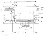
- FIG. 7 is an enlarged view of a region “AA” of FIG. 5 .
- FIG. 8 is a cross-sectional view illustrating the travel of light emitted from an organic light-emitting layer according to one or more embodiments of the invention.
- FIG. 9 is a graph illustrating a ratio of light transmitted from an organic light-emitting layer to a conversion part in accordance with a variation of a second shortest distance illustrated in FIG. 7 .
- FIG. 10 is a graph illustrating a light leakage ratio according to variations of a first shortest distance and a third shortest distance illustrated in FIG. 7 .
- the top surface of the insulating layer PL includes a flat area FA and concave areas BA 1 and BA 2 .
- the organic layer OL 2 overlaps with the first opening OP 1 and is disposed on the first electrode EL 2 a .
- the light-emitting layer EML 2 includes a flat light emitting area FL overlapping with the flat area FA, and concave light emitting areas CL 1 and CL 2 overlapping with the concave areas BA 1 and BA 2 .
- most of light outputted or emitted from the flat light emitting area FL of the light-emitting layer EML 2 may be condensed to the second conversion part CCF 2 . This may be because the flat light emitting area FL overlaps with a central portion of the second conversion part CCF 2 as compared with the concave light emitting areas CL 1 and CL 2 extending with the flat light emitting area FL interposed therebetween.
- the light outputted from the flat light emitting area FL may be more condensed to the second conversion part CCF 2 than light outputted from the concave light emitting areas CL 1 and CL 2 .
- the concave light emitting areas CL 1 and CL 2 are closer to the light shielding member BM than the flat light emitting area FL is, the light is emitted through concave surfaces of the concave light emitting areas CL 1 and CL 2 , thereby improving or increasing efficiency of the light condensed to the second conversion part CCF 2 .
- distance conditions between one light shielding member BM and the concave areas BA 1 and BA 2 and a distance condition between one light shielding member BM and the insulating layer PL will be described. These distance conditions may also be applied to the plurality of light shielding members BM. These distance conditions may be provided to further condense the light outputted from the light-emitting layer EML 2 to the second conversion part CCF 2 .
- one end of the light shielding member BM is opposite to the second opening OP 2 overlapping with the organic layer OL 1 , and another end of the light shielding member BM is adjacent to the second opening OP 2 overlapping with the organic layer OL 2 .
- a first shortest distance D 1 is defined as the shortest distance from the one end of the light shielding member BM to a first boundary axis P 1 between the concave area BA 1 and the flat area FA.
- a second shortest distance D 2 is defined as the shortest distance from the another end of the light shielding member BM to the first boundary axis P 1 .
- the second shortest distance D 2 may be shorter than the first shortest distance D 1 .
- the first boundary axis P 1 may define a boundary between the flat surface and the concave surface of each of the insulating layer PL, the organic layer OL 2 , the first electrode EL 2 a and the second electrode EL 2 b.
- a fifth shortest distance D 5 is defined as the shortest distance from the another end of the light shielding member BM to a second boundary axis P 2 between the concave area BA 2 and the flat area FA.
- the fifth shortest distance D 5 from the another end of the light shielding member BM to the second boundary axis P 2 and the second shortest distance D 2 from the another end of the light shielding member BM to the first boundary axis P 1 may be the same.
- a sixth shortest distance is defined as the shortest distance from the one end of the light shielding member adjacent to the concave area BA 2 to the second boundary axis P 2 .
- the sixth shortest distance is greater than twice the third shortest distance D 3 .
- the fifth shortest distance D 5 is shorter than the sixth shortest distance.
- a third shortest distance D 3 is defined as the shortest distance between the light shielding member BM and the insulating layer PL
- a fourth shortest distance D 4 is defined as a width of the second opening OP 2 between the light shielding members BM.
- the first shortest distance D 1 may be a sum of a width of the light shielding member BM in the first direction DR 1 and the second shortest distance D 2 .
- the width of the light shielding member BM may be substantially constant, and the second shortest distance D 2 may be varied.
- a horizontal axis represents the second shortest distance D 2 , and a unit of the second shortest distance D 2 may be a micrometer ( ⁇ m).
- a vertical axis represents a ratio of the amount (Im) of light condensed to the conversion part CCF 2 .
- the second shortest distance D 2 may be in a range from 1 ⁇ m to 100 ⁇ m.
- the third shortest distance D 3 may be in a range from 10 ⁇ m to 20 ⁇ m.
- the third shortest distance is not limited to the range and may be changed according to one or more embodiments.
- a ratio of the second shortest distance D 2 to the fourth shortest distance D 4 may be greater than 0.005:1 and less than 0.5:1.
- the amount of light condensed to the conversion part CCF 2 may be a first ratio (1.00).
- the second shortest distance D 2 it is considered that there is no overlapping portion between the second opening OP 2 and the concave light emitting areas CL 1 and CL 2 .
- the light-emitting layer EML 2 may include only the flat light emitting area FL.
- the first ratio (1.00) may be defined as a reference ratio at which light is condensed to the conversion part CCF 2 .
- the efficiency of the light condensed to the conversion part CCF 2 may be reduced.
- the efficiency of the light condensed to the conversion part CCF 2 may be increased.
- the amount (Im) of the light may be changed as the second shortest distance D 2 is varied.
- the second shortest distance D 2 increases, widths of the concave light emitting areas CL 1 and CL 2 in the first direction DR 1 may increase.
- the second shortest distance D 2 is greater than 100 ⁇ m, the amount of the light condensed to the conversion part CCF 2 is less than the reference ratio, as illustrated in FIG. 9 .
- the widths of the concave light emitting areas CL 1 and CL 2 increase but a width of the flat light emitting area FL in the first direction DR 1 decreases as the second shortest distance D 2 increases.
- radii of curvature of the concave light emitting areas CL 1 and CL 2 may be increased to cause a light leakage phenomenon.
- the second shortest distance D 2 according to the invention may be in the range from 1 ⁇ m to 100 ⁇ m, as described above. As a result, it is possible to increase or improve the efficiency of the light condensed to the conversion part CCF 2 .
- a horizontal axis represents a ratio between the first shortest distance D 1 and the third shortest distance D 3 .
- a vertical axis represents a light leakage ratio when light emitted from the light-emitting layer is transmitted to another conversion part not overlapping with the light-emitting layer, not the conversion part overlapping with the light-emitting layer.
- the first shortest distance D 1 and the third shortest distance D 3 satisfy the following Equation 1:
- X Y > 2.
- X denotes the first shortest distance D 1
- Y denotes the third shortest distance D 3 .
- the first shortest distance D 1 may be greater than twice the third shortest distance D 3 .
- the ratio between the first and third shortest distances D 1 and D 3 based on the Equation 1 is greater than 2, the light leakage ratio is relatively low.
- the ratio between the first and third shortest distances D 1 and D 3 is equal to or less than 2, the light leakage ratio rapidly increases.
- the amount of the light condensed to the conversion part CCF 2 may be changed according to distance setting between the first and third shortest distances D 1 and D 3 .
- light leakage of the light emitted from the light-emitting layer EML 2 may increase as the third shortest distance D 3 between the light shielding member BM and the insulating layer PL increases.
- the light leakage of the light emitted from the light-emitting layer EML 2 may decrease as the third shortest distance D 3 between the light shielding member BM and the insulating layer PL decreases.
- the efficiency of the light condensed to the conversion part CCF 2 may increase as the light leakage ratio decreases.
- a plurality of layers may be disposed between the light shielding member BM and the insulating layer, and thus the third shortest distance D 3 may increase.
- a filling material may further be disposed between the sealing layer TFE and the conversion part CCF 2 .
- the third shortest distance D 3 may increase as a plurality of component layers is further disposed between the light shielding member BM and the insulating layer PL.
- the light leakage ratio is lowered, as illustrated in FIG. 10 .
- the first shortest distance D 1 is defined as the sum of the width of the light shielding member BM in the first direction DR 1 and the second shortest distance D 2 , a ratio of the second shortest distance D 2 and the third shortest distance D 3 may be substantially varied.
- the width of the light shielding member BM may also be varied.
- the efficiency of the light condensed to the conversion part may be increased or improved.
- the display panel may include the electrode and the light-emitting layer which have the concave area and the flat area. As a result, it is possible to improve the extraction efficiency of the light outputted to the outside through the display surface.
Landscapes
- Engineering & Computer Science (AREA)
- Microelectronics & Electronic Packaging (AREA)
- Physics & Mathematics (AREA)
- Optics & Photonics (AREA)
- Electroluminescent Light Sources (AREA)
Abstract
Description
where “X” is the first shortest distance, and “Y” is the third shortest distance, and the third shortest distance may be fixed.
Here, “X” denotes the first shortest distance D1 and “Y” denotes the third shortest distance D3. In other words, the first shortest distance D1 may be greater than twice the third shortest distance D3. As shown in the graph of
Claims (13)
Applications Claiming Priority (2)
| Application Number | Priority Date | Filing Date | Title |
|---|---|---|---|
| KR10-2017-0060144 | 2017-05-15 | ||
| KR1020170060144A KR102401398B1 (en) | 2017-05-15 | 2017-05-15 | Organic electroluminescence display apparatus |
Publications (2)
| Publication Number | Publication Date |
|---|---|
| US20180331316A1 US20180331316A1 (en) | 2018-11-15 |
| US10600985B2 true US10600985B2 (en) | 2020-03-24 |
Family
ID=64097995
Family Applications (1)
| Application Number | Title | Priority Date | Filing Date |
|---|---|---|---|
| US15/839,652 Active 2038-01-03 US10600985B2 (en) | 2017-05-15 | 2017-12-12 | Organic electroluminescence display apparatus |
Country Status (2)
| Country | Link |
|---|---|
| US (1) | US10600985B2 (en) |
| KR (1) | KR102401398B1 (en) |
Cited By (1)
| Publication number | Priority date | Publication date | Assignee | Title |
|---|---|---|---|---|
| US12520695B2 (en) | 2022-02-08 | 2026-01-06 | Samsung Display Co., Ltd. | Display apparatus including layer enhancing color purity by passing light of predetermined wavelngth range |
Families Citing this family (11)
| Publication number | Priority date | Publication date | Assignee | Title |
|---|---|---|---|---|
| KR102502221B1 (en) | 2017-08-08 | 2023-02-21 | 삼성디스플레이 주식회사 | Color conversion element and display device comprising the same |
| KR102597018B1 (en) * | 2018-08-23 | 2023-10-31 | 엘지디스플레이 주식회사 | Display device and method of manufacturing the same |
| KR101977322B1 (en) | 2018-10-22 | 2019-05-10 | 경창산업주식회사 | Self-energizing Brake Caliper |
| KR102827287B1 (en) * | 2019-01-28 | 2025-07-01 | 삼성디스플레이 주식회사 | Display device and method of manufacturing the same |
| CN110112189B (en) * | 2019-04-25 | 2021-03-23 | 武汉华星光电半导体显示技术有限公司 | Display panel and display device |
| CN119584803A (en) * | 2019-11-06 | 2025-03-07 | 乐金显示有限公司 | Display Panel |
| KR102510120B1 (en) | 2019-11-06 | 2023-03-15 | 엘지디스플레이 주식회사 | Touch display device |
| KR102945861B1 (en) | 2020-02-03 | 2026-03-31 | 삼성디스플레이 주식회사 | Color conversion substrate, and display device for the same |
| KR102840679B1 (en) * | 2020-09-01 | 2025-07-31 | 삼성디스플레이 주식회사 | Display device |
| KR20220030461A (en) | 2020-09-01 | 2022-03-11 | 삼성디스플레이 주식회사 | Display device |
| KR20230068496A (en) | 2021-11-10 | 2023-05-18 | 삼성디스플레이 주식회사 | Display device and method of manufacturing the same |
Citations (8)
| Publication number | Priority date | Publication date | Assignee | Title |
|---|---|---|---|---|
| KR100546661B1 (en) | 2003-08-04 | 2006-01-26 | 엘지전자 주식회사 | Organic EL display element |
| US20060284532A1 (en) * | 2005-06-15 | 2006-12-21 | Makoto Kurihara | Color display unit |
| KR100709194B1 (en) | 2005-11-23 | 2007-04-18 | 삼성에스디아이 주식회사 | OLED display and manufacturing method thereof |
| KR20090021709A (en) | 2007-08-28 | 2009-03-04 | 엘지전자 주식회사 | Electroluminescent element and manufacturing method thereof |
| KR20130008892A (en) | 2011-07-13 | 2013-01-23 | 엘지디스플레이 주식회사 | Quantum-dot light emitting diode and method for fabricating the same |
| US20140291648A1 (en) * | 2013-03-28 | 2014-10-02 | Semiconductor Energy Laboratory Co., Ltd. | Light-Emitting Device |
| US20150102330A1 (en) * | 2013-10-14 | 2015-04-16 | Sumitomo Chemical Co. Limited | Composition and device |
| US20160163768A1 (en) | 2014-12-09 | 2016-06-09 | Samsung Display Co., Ltd. | Organic light emitting display and manufacturing method thereof |
Family Cites Families (1)
| Publication number | Priority date | Publication date | Assignee | Title |
|---|---|---|---|---|
| KR100615199B1 (en) * | 2003-11-29 | 2006-08-25 | 삼성에스디아이 주식회사 | Organic electroluminescent display |
-
2017
- 2017-05-15 KR KR1020170060144A patent/KR102401398B1/en active Active
- 2017-12-12 US US15/839,652 patent/US10600985B2/en active Active
Patent Citations (10)
| Publication number | Priority date | Publication date | Assignee | Title |
|---|---|---|---|---|
| KR100546661B1 (en) | 2003-08-04 | 2006-01-26 | 엘지전자 주식회사 | Organic EL display element |
| US20060284532A1 (en) * | 2005-06-15 | 2006-12-21 | Makoto Kurihara | Color display unit |
| KR100709194B1 (en) | 2005-11-23 | 2007-04-18 | 삼성에스디아이 주식회사 | OLED display and manufacturing method thereof |
| KR20090021709A (en) | 2007-08-28 | 2009-03-04 | 엘지전자 주식회사 | Electroluminescent element and manufacturing method thereof |
| KR20130008892A (en) | 2011-07-13 | 2013-01-23 | 엘지디스플레이 주식회사 | Quantum-dot light emitting diode and method for fabricating the same |
| US20140291648A1 (en) * | 2013-03-28 | 2014-10-02 | Semiconductor Energy Laboratory Co., Ltd. | Light-Emitting Device |
| JP2014209480A (en) | 2013-03-28 | 2014-11-06 | 株式会社半導体エネルギー研究所 | Light emitting device |
| US20150102330A1 (en) * | 2013-10-14 | 2015-04-16 | Sumitomo Chemical Co. Limited | Composition and device |
| US20160163768A1 (en) | 2014-12-09 | 2016-06-09 | Samsung Display Co., Ltd. | Organic light emitting display and manufacturing method thereof |
| KR20160070272A (en) | 2014-12-09 | 2016-06-20 | 삼성디스플레이 주식회사 | Organic light emitting display and manufacturing method thereof |
Cited By (1)
| Publication number | Priority date | Publication date | Assignee | Title |
|---|---|---|---|---|
| US12520695B2 (en) | 2022-02-08 | 2026-01-06 | Samsung Display Co., Ltd. | Display apparatus including layer enhancing color purity by passing light of predetermined wavelngth range |
Also Published As
| Publication number | Publication date |
|---|---|
| KR20180125673A (en) | 2018-11-26 |
| KR102401398B1 (en) | 2022-05-25 |
| US20180331316A1 (en) | 2018-11-15 |
Similar Documents
| Publication | Publication Date | Title |
|---|---|---|
| US10600985B2 (en) | Organic electroluminescence display apparatus | |
| US9748321B2 (en) | Organic light-emitting diode display | |
| EP2963687B1 (en) | Organic electroluminescent device | |
| JP4910780B2 (en) | Organic electroluminescence device with input function and electronic device | |
| KR102508750B1 (en) | Light emitting display device | |
| US9921670B2 (en) | Organic light emitting display | |
| US9466810B2 (en) | Organic light emitting diode display | |
| CN113013349B (en) | Display device | |
| CN110010658B (en) | Display device | |
| US9331301B2 (en) | Active matrix organic light-emitting display and display apparatus | |
| US11387294B2 (en) | Display device | |
| US10665820B2 (en) | Display device | |
| US9190624B2 (en) | Organic light emitting diode display | |
| US12382808B2 (en) | Display apparatus including overlapping elements | |
| US20220059637A1 (en) | Display apparatus | |
| US10997921B2 (en) | Organic light-emitting display device | |
| US10784459B2 (en) | Display device | |
| US20230329050A1 (en) | Display device | |
| KR20240119586A (en) | Display Device Having MUX Part And Method Of Driving The Same | |
| US20240257685A1 (en) | Display device | |
| US10446075B2 (en) | Organic light emitting diode display device | |
| KR20240067187A (en) | Display device | |
| KR20240025132A (en) | Display device | |
| KR20240079709A (en) | Light emitting display device | |
| KR20250118298A (en) | display device |
Legal Events
| Date | Code | Title | Description |
|---|---|---|---|
| AS | Assignment |
Owner name: SAMSUNG DISPLAY CO., LTD., KOREA, REPUBLIC OF Free format text: ASSIGNMENT OF ASSIGNORS INTEREST;ASSIGNORS:LEE, JUNEWOO;JEONG, BYOUNGSEONG;KIM, JI-HYUN;AND OTHERS;REEL/FRAME:044375/0129 Effective date: 20171013 |
|
| FEPP | Fee payment procedure |
Free format text: ENTITY STATUS SET TO UNDISCOUNTED (ORIGINAL EVENT CODE: BIG.); ENTITY STATUS OF PATENT OWNER: LARGE ENTITY |
|
| STPP | Information on status: patent application and granting procedure in general |
Free format text: NON FINAL ACTION MAILED |
|
| STPP | Information on status: patent application and granting procedure in general |
Free format text: RESPONSE TO NON-FINAL OFFICE ACTION ENTERED AND FORWARDED TO EXAMINER |
|
| STPP | Information on status: patent application and granting procedure in general |
Free format text: FINAL REJECTION MAILED |
|
| STPP | Information on status: patent application and granting procedure in general |
Free format text: NOTICE OF ALLOWANCE MAILED -- APPLICATION RECEIVED IN OFFICE OF PUBLICATIONS |
|
| STPP | Information on status: patent application and granting procedure in general |
Free format text: PUBLICATIONS -- ISSUE FEE PAYMENT VERIFIED |
|
| STCF | Information on status: patent grant |
Free format text: PATENTED CASE |
|
| MAFP | Maintenance fee payment |
Free format text: PAYMENT OF MAINTENANCE FEE, 4TH YEAR, LARGE ENTITY (ORIGINAL EVENT CODE: M1551); ENTITY STATUS OF PATENT OWNER: LARGE ENTITY Year of fee payment: 4 |