US10598890B2 - Lens assembly and electronic device including the same - Google Patents
Lens assembly and electronic device including the same Download PDFInfo
- Publication number
- US10598890B2 US10598890B2 US15/368,551 US201615368551A US10598890B2 US 10598890 B2 US10598890 B2 US 10598890B2 US 201615368551 A US201615368551 A US 201615368551A US 10598890 B2 US10598890 B2 US 10598890B2
- Authority
- US
- United States
- Prior art keywords
- lens
- cut
- spacer
- disposed
- barrel
- Prior art date
- Legal status (The legal status is an assumption and is not a legal conclusion. Google has not performed a legal analysis and makes no representation as to the accuracy of the status listed.)
- Active, expires
Links
Images


Classifications
-
- G—PHYSICS
- G02—OPTICS
- G02B—OPTICAL ELEMENTS, SYSTEMS OR APPARATUS
- G02B7/00—Mountings, adjusting means, or light-tight connections, for optical elements
- G02B7/02—Mountings, adjusting means, or light-tight connections, for optical elements for lenses
- G02B7/021—Mountings, adjusting means, or light-tight connections, for optical elements for lenses for more than one lens
-
- G—PHYSICS
- G02—OPTICS
- G02B—OPTICAL ELEMENTS, SYSTEMS OR APPARATUS
- G02B13/00—Optical objectives specially designed for the purposes specified below
- G02B13/001—Miniaturised objectives for electronic devices, e.g. portable telephones, webcams, PDAs, small digital cameras
- G02B13/0015—Miniaturised objectives for electronic devices, e.g. portable telephones, webcams, PDAs, small digital cameras characterised by the lens design
- G02B13/002—Miniaturised objectives for electronic devices, e.g. portable telephones, webcams, PDAs, small digital cameras characterised by the lens design having at least one aspherical surface
Definitions
- Various embodiments of the present disclosure relate to an electronic device, for example, a lens assembly for providing a photographing function and an electronic device including the lens assembly.
- An electronic device for example, a camera capable of capturing still images or moving images has already been popularized. Recently, an electronic device such as a digital camera, a video camera, or the like, having a solid image sensor, for example, a charge coupled device, a complementary metal-oxide semiconductor, etc., has come into wide use. An electronic device using a solid image sensor like a CCD or a CMOS gradually substitutes for an optical device adopting a film scheme because of easiness in storage, copy, and movement of images when compared to the film-scheme optical device.
- a lens assembly and/or an electronic device may include at least one lens.
- a high-performance lens assembly capable of obtaining high resolution and high-brightness images may include a plurality of lenses.
- a primary object to provide a lens assembly which is easy to miniaturize while contributing to obtaining high-quality images and/or videos, and an electronic device including the lens assembly.
- a lens assembly including a lens that includes an effective region that refracts light, a flange region formed on at least a part around the effective region, and a first cut formed on a first sub region of the flange region, a spacer that includes a second cut formed to correspond to the first cut, and a barrel configured to receive the lens and the spacer, in which the lens and the spacer are disposed inside the barrel such that the first cut and the second cut correspond to a third cut formed on an outer circumferential surface of the barrel.
- an electronic device including a lens in which a first cut is formed on a first sub region of a flange, a spacer in which a second cut is formed on a second sub region, and a barrel in which a third cut is formed on a third sub region of an edge portion, in which the first sub region, the second sub region, and the third sub region are disposed to correspond to each other.
- a lens assembly including at least one lens comprising a circular effective region that refracts light and a flange formed along a circumference of the effective region, in which the flange comprises at least one first D-shape plane and a portion of the effective region protrudes outwardly from the first D-shape plane.
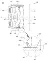
- FIG. 1 illustrates a perspective view of a lens assembly according to various embodiments of the present disclosure
- FIG. 2 illustrates a plane view of a lens assembly according to various embodiments of the present disclosure
- FIG. 3 illustrates a cross-sectional view of an electronic device including a lens assembly according to various embodiments of the present disclosure
- FIG. 4 illustrates a cross-sectional view of an electronic device including a lens assembly according to various embodiments of the present disclosure
- FIG. 5 illustrates a plane view of a lens of a lens assembly according to various embodiments of the present disclosure
- FIG. 6 illustrates a cross-sectional view of a lens of a lens assembly according to various embodiments of the present disclosure
- FIG. 7 illustrates a plane view of one a lens of a lens assembly according to various embodiments of the present disclosure
- FIG. 8 illustrates a plane view of a lens of lens assembly according to various embodiments of the present disclosure
- FIG. 9 illustrates a plane view of a lens of a lens assembly according to various embodiments of the present disclosure
- FIG. 10 illustrates a plane view of a spacer of a lens assembly according to various embodiments of the present disclosure
- FIG. 11 illustrates a plane view of a spacer of a lens assembly according to various embodiments of the present disclosure
- FIG. 12 illustrates a plane view of a plurality of lenses arranged in a lens assembly according to various embodiments of the present disclosure
- FIG. 13 illustrates a block diagram of an electronic device according to various embodiments of the present disclosure.
- FIG. 14 illustrates a cross-sectional view of a lens assembly according to various embodiments of the present disclosure.
- FIGS. 1 through 14 discussed below, and the various embodiments used to describe the principles of the present disclosure in this patent document are by way of illustration only and should not be construed in any way to limit the scope of the disclosure. Those skilled in the art will understand that the principles of the present disclosure may be implemented in any suitably arranged electronic device.
- an expression such as “A or B,” “at least one of A or/and B,” or “one or more of A or/and B” may include all possible combinations of together listed items.
- “A or B,” “at least one of A and B,” or “one or more of A or B” may indicate the entire of (1) including at least one A, (2) including at least one B, or (3) including both at least one A and at least one B.
- first, second, primarily,” or “secondary,” used herein may represent various elements regardless of order and/or importance and do not limit corresponding elements.
- a first user device and a second user device may represent different user devices regardless of order or importance.
- a first element may be named as a second element without departing from the right scope of the various exemplary embodiments of the present disclosure, and similarly, a second element may be named as a first element.
- an element such as a first element
- another element such as a second element
- the element can be directly connected to the other element or can be connected to the other element through another element (e.g., a third element).
- an element such as a first element
- another element such as a second element
- An expression “configured to (or set)” used in the present disclosure may be replaced with, for example, “suitable for,” “having the capacity to,” “designed to,” “adapted to,” “made to,” or “capable of” according to a situation.
- a term “configured to (or set)” does not always mean only “specifically designed to” by hardware.
- an expression “apparatus configured to” may mean that the apparatus “can” operate together with another apparatus or component.
- a phrase “a processor configured (or set) to perform A, B, and C” may be a dedicated processor (e.g., an embedded processor) for performing a corresponding operation or a generic-purpose processor (such as a CPU or an application processor) that can perform a corresponding operation by executing at least one software program stored at a memory device.
- a dedicated processor e.g., an embedded processor
- a generic-purpose processor such as a CPU or an application processor
- an electronic device may be an arbitrary device including a lens assembly and may be referred to as a terminal, a portable terminal, a mobile terminal, a communication terminal, a portable communication terminal, a portable mobile terminal, a display, or the like.
- the electronic device may be a smart phone, a cellular phone, a navigation device, a game console, a television (TV), a vehicle head unit, a laptop computer, a tablet computer, a personal media player (PMP), a personal digital assistant (PDA), or the like, which has a lens assembly mounted thereon.
- the electronic device may be implemented with a pocket-size portable communication terminal having a wireless communication function.
- the electronic device may be a flexible device or a flexible display.
- the electronic device may communicate with an external electronic device such as a server or may work by cooperating with the external electronic device. For example, the electronic device may transmit an image captured by a camera and/or position information detected by a sensor unit to the server over a network.
- a network may be, but not limited to, a mobile or cellular communication network, a local area network (LAN), a wireless local area network (WLAN), a wide area network (WAN), Internet, a small area network (SAN), or the like.
- FIG. 1 illustrates a perspective view of a lens assembly 100 according to various embodiments of the present disclosure.
- the lens assembly 100 may include a barrel 101 that receives at least one lens.
- the barrel 101 may be, globally, in a cylindrical shape and may include, on a top surface thereof, an opening into which light is incident.
- the lens received in the barrel 101 is exposed through the opening to refract the light (e.g., image information about an object) incident from the outside.
- the barrel 101 may include a D-shape plane 111 formed on a partial region (e.g., a sub region) of an outer circumferential surface thereof.
- the ‘D-shape plane’ may mean an edge portion in a circular or curved shape or a linear or plane portion formed by removing a part of a curved surface.
- the ‘D-shape plane’ may be referred to as ‘D cut’ or ‘nth cut’.
- a driving device e.g., a magnetic portion, a coil, a shape memory alloy, etc.
- the magnetic portion may be disposed on the D-shape plane 111 .
- FIG. 2 illustrates a plane view of a lens assembly 200 according to various embodiments of the present disclosure.
- the lens assembly 200 may include a barrel 201 including a D-shape plane 211 formed on a partial region of an outer circumferential surface thereof, e.g., a sub region 213 .
- the barrel 201 may include a plane portion formed by removing a part of the outer circumferential surface. As a part of the outer circumferential surface of the barrel 201 globally in the cylindrical shape is removed, the size (e.g., volume) of the lens assembly 200 may be reduced.
- the lens assembly 200 may include a lens 202 exposed on a surface (e.g., a top surface) of the barrel 201 as being received in the barrel 201 .
- FIG. 3 illustrates a cross-sectional view of an electronic device 300 including a lens assembly after a part of the electronic device 300 is cut, according to various embodiments of the present disclosure, and may include, for example, a cross section of the lens assembly 200 , cut along a line A-A shown in FIG. 2 .
- the electronic device 300 may include a barrel 301 that receives at least one of lenses 321 and 323 and an image sensor 343 .
- the plurality of lenses 321 and 323 may be arranged in the barrel 301 along an optical axis O-I, e.g., from an object side O to an image sensor side I.
- the lenses 321 and 323 refract the incident light from the object side O to the barrel 301 to cause the light to be incident into an imaging surface of the image sensor 343 .
- 6 lenses are arranged inside the barrel 301 in FIG. 3 , reference numerals are given to only some of the 6 lenses for brevity of the drawings.
- the number of lenses mounted on the electronic device 300 is not necessarily limited to 6. For example, depending on specifications required for the electronic device 300 , the number of lenses may be greater than or less than 6.
- the lenses 321 and 323 may have identical diameters from the lens disposed in the object side O to the lens disposed in the image sensor side I, or may sequentially have greater diameters toward the image sensor side I. In an embodiment, some lenses may have identical diameters and some other lenses may sequentially have greater diameters toward the image sensor side I.
- the image sensor 343 is mounted on a circuit board 341 and arranged in alignment with the optical axis O-I of the lenses 321 and 323 .
- the image sensor 343 detects contrast information, grayscale information, color information, and so forth regarding an object from the light incident through the lenses 321 and 323 and obtains an image for the object.
- the electronic device 300 may include a processor, a memory, a display, and the like that are not shown, the processor may generate an image based on information detected by the image sensor 343 , and the generated image (and/or image file) may be stored in a memory or output through a display.
- the lens assembly e.g., the lens assemblies 100 and 200 shown in FIG. 1 and/or FIG. 2
- the electronic device 300 may include at least one spacer 303 disposed between two adjacent lenses, if including a plurality of lenses.
- the spacer 303 maintains a space between two adjacent lenses (e.g., the lenses 321 and 323 ).
- the spacer 303 may have a thickness (for example, measured along the optical axis O-I) varying depending on a position of the spacer 303 .
- a spacer disposed between the lens closest to the object side O and a lens adjacent thereto may have a smaller thickness than a spacer disposed between the lens closest to the image sensor side I and a lens adjacent thereto.
- spacers may be disposed between some of the lenses and no space may be disposed between some other of the lenses.
- FIG. 4 is a cross-sectional view of an electronic device 400 including a lens assembly after a part of the electronic device 300 is cut, according to various embodiments of the present disclosure, and may include, for example, a cross section of the lens assembly 200 , cut along a line B-B shown in FIG. 2 .
- the electronic device 400 may include a barrel 401 that receives at least one lenses 421 and 423 and an image sensor 443 .
- the plurality of lenses 421 and 423 may be arranged in the barrel 401 along the optical axis O-I, e.g., from the object side O to the image sensor side I.
- the lenses 421 and 423 refract the incident light from the object side O to the barrel 401 to cause the light to be incident into an imaging surface of the image sensor 443 .
- the lenses 421 and 423 may have identical diameters from the lens disposed in the object side O to the lens disposed in the image sensor side I, or may sequentially have greater diameters toward the image sensor side I. In an embodiment, some lenses may have identical diameters, and some other lenses may have greater diameters which may be disposed on the image sensor side.
- the image sensor 443 is mounted on a circuit board 441 and arranged in alignment with the optical axis O-I of the lenses 421 and 423 .
- the image sensor 443 detects contrast information, grayscale information, color information, and so forth regarding an object from the light incident through the lenses 421 and 423 and obtains an image for the object.
- the lens assembly e.g., the lens assemblies 100 and 200 shown in FIG. 1 and/or FIG. 2
- the electronic device 400 may include at least one spacer 403 disposed between two adjacent lenses, if including a plurality of lenses.
- the spacer 403 maintains a space between two adjacent lenses (e.g., the lenses 421 and 423 ).
- the spacer 403 may have a thickness (for example, measured along the optical axis O-I) varying depending on a position of the spacer 303 .
- a spacer disposed between the lens closest to the object side O and a lens adjacent thereto may have a smaller thickness than a spacer disposed between the lens closest to the image sensor side I and a lens adjacent thereto.
- spacers may be disposed between some of the lenses and no space may be disposed between some other of the lenses.
- the lenses 421 and 423 and/or the spacer 403 may include planes 425 and 431 corresponding to a D-shape plane 411 of the barrel 401 (e.g., the D-shape planes 111 and 211 of FIG. 1 and/or FIG. 2 ).
- the lenses 421 and 423 and/or the spacer 403 may globally have a disc shape or a ring shape, but may include a linear edge portion (e.g., the planes 425 and 431 ) by removing a partial region (e.g., a sub region) of the edge.
- the plane portion included in the lens 423 and/or the spacer 403 e.g., the D cut will be described in more detail with reference to FIG. 7 .
- the lenses 421 and 423 and/or the spacer 403 may be received inside the barrel 401 such that the D-shape planes or the D cuts (e.g., the planes 425 and 431 ) formed on the lenses 421 and 423 and/or the spacer 403 are aligned to correspond to the D-shape plane 411 formed on the barrel 401 .
- the diameter (or radius) of the lens in a portion where the D cut (e.g., the plane 425 ) is formed may be less than that in the other portion (e.g., a portion where the D cut is not formed).
- the lenses 421 and 423 and/or the barrel 401 may perform auto focusing while reciprocating with respect to the image sensor 443 along the optical axis O-I.
- various driving devices e.g., a voice coil motor, a step motor, an ultrasonic motor, a piezoelectric device, and the like may be used.
- the driving device may be mounted on the D-shape plane 411 formed on the outer circumferential surface of the barrel 401 .
- the driving device is implemented with a voice coil motor including a coil portion and the magnetic portion 404 , the magnetic portion 404 may be mounted on the D-shape plane 411 .
- FIG. 5 is a plane view for describing a lens of a lens assembly 502 according to various embodiments of the present disclosure.
- FIG. 6 is a plane view illustrating a lens of a lens assembly 602 according to various embodiments of the present disclosure.
- lenses 502 and 602 may include effective regions 523 and 623 and flange regions 527 and 627 formed along circumferences of the effective regions 523 and 623 , respectively.
- the effective regions 523 and 623 are regions for refracting incident light
- the lenses 502 and 602 may include lens portions 521 and 621 formed on the effective regions 523 and 623 , respectively.
- the lens portions 521 and 621 may refract incident light by having a positive or negative refractive force.
- On the flange regions 527 and 627 may be formed flanges 525 and 625 extending outwardly with respect to the lens portions 521 and 621 along the circumferences of the lens portions 521 and 621 .
- the flanges 525 and 625 may provide a means for mounting and fixing the lenses 502 and 602 onto another structure, e.g., the barrel 401 shown in FIG. 4 .
- the flanges 525 and 625 are bound or fixed to the inside of the barrel (e.g., the barrel 401 of FIG. 4 )
- the lenses 502 and 602 may be mounted inside the barrel without the structure of the barrel being interfered by the effective regions 523 and 623 .
- the D cut is formed by removing a part of the flanges 525 and 625 , thereby miniaturizing the lens assembly (e.g., the lens assemblies 100 and 200 of FIG. 1 and/or FIG. 2 ) and/or an electronic device (e.g., the lens assemblies 300 and 400 of FIG. 3 and/or FIG. 4 ) while guaranteeing optical performance thereof.
- the optical performance of the lens assembly and/or the electronic device may be guaranteed by maintaining the effective regions 523 and 623 of the lenses 502 and 602 , and the lens assembly and/or the electronic device may be miniaturized by removing a part of the flanges 525 and 625 .
- an embodiment of the miniaturized lens which maintains the effective region will be described with reference to FIG. 7 .
- FIG. 7 is a plane view of one lens 702 of a lens assembly according to various embodiments of the present disclosure.
- one lens of the above-described lens assembly may include a first cut 725 (e.g., the D-shape plane 425 of FIG. 4 ) formed on a sub region 723 b in a flange region 723 a .
- the lens 702 may include a lens portion 721 formed in an effective region and a flange 723 formed on a circumference of the lens portion 721 .
- the effective region for example, the lens portion 721 may have a circular shape, and the flange 723 may have a ring shape formed on a circumference of the lens portion 721 .
- a part of an edge of the flange 723 may have a linear shape.
- the edge of the flange 723 may globally have a circular shape and a portion thereof may include the first cut 725 in a linear shape.
- a pair of first cuts 725 may be formed on edges of the flange 723 , respectively, and may be arranged symmetrically with respect to the effective region, e.g., the center of the lens portion 721 .
- the first cuts 725 may be formed in an upper portion and a lower portion of the lens portion 721 , respectively, and the first cuts 725 may be arranged symmetrically with respect to the lens portion 721 .
- the lens 702 may satisfy: CA ⁇ D ⁇ L ⁇ 1.08 CA (1),
- ‘D’ indicates a radius of the lens 702 (e.g., a radius of a portion where the first cut 725 is not formed)
- ‘L’ indicates a length of a removed portion of the flange 723 after formation of the first cut 725
- ‘CA’ indicates a radius of the effective region, e.g., a radius of the lens portion 721 .
- ‘D-L’ indicates a distance from the center of the lens portion 721 to the first cut 725 .
- the lens portion 721 is surrounded by the flange 723 .
- the flange 723 may have a ring shape that encloses the entire circumference of the lens portion 721 while including the first cut 725 .
- FIG. 8 is a plane view of another lens 802 of the plurality of lenses of a lens assembly according to various embodiments of the present disclosure.
- one lens 802 of the plurality of lenses of the above-described lens assembly may include a first cut 825 (e.g., the D-shape plane 425 of FIG. 4 ) formed on a sub region in a flange region.
- the lens 802 may include a lens portion 821 formed in an effective region and a flange 823 formed on a circumference of the lens portion 821 .
- the effective region for example, the lens portion 821 may have a circular shape, and the flange 823 may have a ring shape formed on a circumference of the lens portion 821 .
- a part of an edge of the flange 823 may have a first cut 825 .
- a pair of or two pairs of first cuts 825 may be arranged symmetrically with respect to the center of the lens portion 821 , and a portion of an effective region, e.g., a portion of the lens portion 821 may protrude outwardly from the first cut 825 .
- the lens 802 may satisfy: D ⁇ L ⁇ CA (2),
- ‘D’ indicates a radius of the lens 802
- ‘L’ indicates a length of a removed portion of the flange 823 after formation of the first cut 825
- ‘CA’ indicates a radius of the effective region, e.g., a radius of the lens portion 821
- ‘D-L’ indicates a distance from the center of the lens portion 821 to the first cut 825 (e.g., a virtual straight line C passing through the first cut 825 ).
- the first cut(s) 825 are disposed spaced apart from each other in an upper portion and a lower portion of the lens portion 821 , respectively.
- the first cuts 825 may be positioned on opposite sides of a portion of the lens portion 821 protruding outwardly.
- the straight line C may be situated to partially traverse an effective region of the lens 802 .
- Equation (2) in the structure where the first cut 825 is formed, the lens portion 823 is disposed on opposite sides of the lens portion 821 .
- FIG. 9 is a plane view illustrating one lens 902 of a plurality of lenses of a lens assembly according to various embodiments of the present disclosure.
- a lens 902 of the plurality of lenses of the lens assembly may include a ring-shape flange 923 formed on a circumference of a circular-shape lens portion 921 , and may include a linear-shape first cut 925 formed after a part of an edge of the flange 923 is removed.
- ‘D’ indicates a radius of the lens 902
- ‘L’ indicates a length of a removed portion of the flange 923 after formation of the first cut 925
- ‘CA’ indicates a radius of the effective region, e.g., a radius of the lens portion 921 .
- ‘D-L’ indicates a distance from the center of the lens portion 921 to the first cut 925 .
- the first cut 925 may be positioned in a distance equal to a radius of the lens portion 921 from the center of the lens portion 921 .
- FIG. 10 is a plane view of one spacer 1003 in a plurality of spacers of a lens assembly according to various embodiments of the present disclosure.
- a spacer e.g., the spacer 403 of FIG. 4
- adjacent lenses e.g., the lenses 421 and 423 of FIG. 4
- the spacer 1003 may maintain an interval between adjacent lenses without being interfered by light refracted by the lens portion (e.g., the effective region).
- the spacer 1003 may be formed to correspond to a shape of the flange (e.g., the flange 823 of FIG. 8 ).
- the spacer 1003 may be provided as one pair, and may have a shape corresponding to the flange(s) 823 of the lens 802 shown in FIG. 8 .
- a second pair of spacers 1003 may be disposed to globally have a circular shape and may include a second cut 1031 formed in a sub region 1033 .
- the second cut 1031 may be positioned to correspond to a first cut (e.g., the first cut 825 of FIG. 8 ) formed in a sub region of the flange (e.g., the flange 823 of FIG. 8 ).
- flanges of the first lens and the second lens may face the spacer 1003 , e.g., may contact the spacer 1003 .
- light refracted through the effective regions of the first lens and the second lens may arrive at the image sensor without being interfered by the spacer 1003 .
- FIG. 11 is a plane view illustrating a spacer 1103 of a plurality of spacers of a lens assembly according to various embodiments of the present disclosure.
- the spacer 1103 may have a ring shape (e.g., a closed loop shape) including a second cut 1131 formed in a sub region 1133 .
- FIG. 12 is a plane view illustrating a plurality of lenses 1201 and 1202 arranged in a lens assembly 1200 according to various embodiments of the present disclosure.
- the spacer (the spacers 1003 and 1103 of FIG. 10 and/or FIG. 11 ) has been omitted to show relative sizes of the lenses 1201 and 1202 .
- the relative sizes of the first lens 1201 and the second lens 1202 shown in FIG. 12 are not intended to limit the present disclosure, and may vary according to specifications required in a lens assembly or an electronic device to be manufactured and/or according to a mounting structure, or the like.
- the second lens 1202 may be disposed closer to an image sensor side than the first lens 1201 , and the effective region of at least the second lens 1202 may have a greater radius than the effective region of the first lens 1201 .
- a lens assembly 1200 (e.g., the lens assemblies 100 and 200 of FIG. 1 and/or FIG. 2 ) and/or an electronic device (e.g., the electronic devices 300 and 400 of FIG. 3 and/or FIG. 4 ) according to various embodiments of the present disclosure may include a first lens 1201 positioned on an object side and a second lens 1202 positioned on an image sensor side, and a diameter and/or a radius of the second lens 1202 may be greater than a diameter and/or a radius of the first lens 1201 .
- the effective region of the second lens 1202 may have a diameter and/or a radius greater than the diameter and/or the radius of the first lens 1201 .
- the lens portion 1221 of the second lens 1202 may have a greater diameter than that of at least a lens portion 1211 of the first lens 1201 .
- the lens portion 1221 of the second lens 1202 may have a greater diameter than the entire diameter (e.g., a diameter including a flange 1213 ) of the first lens 1201 .
- a first cut 1225 may be formed on the second lens 1202 , and the first cut 1225 may be formed in a sub region of the second lens 1202 at least based on the diameter of the first lens 1201 .
- the diameter of the second lens 1202 may be greater than that of the first lens 1201 , and at least a part of the first cut 1225 may be formed outward with respect to the first lens 1201 , e.g., the flange 1213 of the first lens 1201 .
- the lens assembly may include a flange on a circumference of an effective region that refracts light and a lens including a D-shape plane in a sub region of the flange.
- the lens may secure optical performance by maintaining a designed effective region while being miniaturized in the entire size.
- FIG. 13 is a block diagram illustrating an electronic device 20 according to various embodiments of the present disclosure.
- the electronic device 20 may include the entire lens assembly illustrated 100 in FIG. 1 or a part of the lens assembly 100 , for example the barrel 101 illustrated in FIG. 1 .
- the electronic device 20 may include one or more processors (e.g., application processors (APs)) 21 , a communication module 22 , a subscriber identification module (SIM) 22 g , a memory 23 , a sensor module 24 , an input module 25 , a display 26 , an interface 27 , an audio module 28 , a camera module 29 a , an indicator 29 b , a motor 29 c , a power management module 29 d , and a battery 29 e.
- processors e.g., application processors (APs)
- SIM subscriber identification module
- the AP 21 controls multiple hardware or software components connected to the AP 21 by driving an operating system (OS) or an application program, and performs processing and operations with respect to various data.
- the AP 21 may be implemented with, for example, a system on chip (SoC).
- SoC system on chip
- the AP 21 may further include a graphic processing unit (GPU) and/or an image signal processor.
- the AP 21 may include at least some of the elements illustrated in FIG. 13 (e.g., the cellular module 22 a ).
- the AP 21 loads a command or data received from at least one of other elements (e.g., a non-volatile memory) into a volatile memory to process the command or data, and stores various data in the non-volatile memory.
- the communication module 22 may include, for example, at least one of the cellular module 22 a , a WiFi module 22 b , a Bluetooth® (BT) module 22 c , a GNSS module 22 d , a near field communication (NFC) module 22 e , and a radio frequency (RF) module 22 f.
- BT Bluetooth®
- NFC near field communication
- RF radio frequency
- the cellular module 22 a may provide, for example, a voice call, a video call, a text service, or an Internet service over a communication network.
- the cellular module 22 a identifies and authenticates the electronic device 20 in a communication network by using the SIM 22 g (e.g., a SIM card).
- the cellular module 22 performs at least one of functions that may be provided by the AP 21 .
- the cellular module 22 may include a communication processor (CP).
- Each of the WiFi module 22 b , the BT module 22 c , the GNSS module 22 d , and the NFC module 22 e may include, for example, a processor for processing data transmitted and received by a corresponding module.
- at least some (e.g., two or more) of the cellular module 22 a , the WiFi module 22 b , the BT module 22 c , the GNSS module 22 d , and the NFC module 22 e may be included in one integrated chip (IC) or IC package.
- IC integrated chip
- the RF module 22 f may, for example, transmit and receive a communication signal (e.g., an RF signal).
- the RF module 22 f may include a transceiver, a power amplifier module (PAM), a frequency filter, a low noise amplifier (LNA), or an antenna.
- PAM power amplifier module
- LNA low noise amplifier
- at least one of the cellular module 22 a , the WiFi module 22 b , the BT module 22 c , the GNSS module 22 d , and the NFC module 22 e may transmit and receive an RF signal through the separate RF module.
- the SIM (e.g., an SIM card) 22 g may, for example, include a card including an SIM and/or an embedded SIM, and may include unique identification information (e.g., an integrated circuit card identifier (ICCID) or subscriber information (e.g., an international mobile subscriber identity (IMSI)).
- ICCID integrated circuit card identifier
- IMSI international mobile subscriber identity
- the memory 23 may include an internal memory 23 a or an external memory 23 b .
- the internal memory 23 a may, for example, include at least one of a volatile memory (e.g., dynamic random access memory (DRAM), static RAM (SRAM), synchronous dynamic RAM (SDRAM), etc.), and a non-volatile memory (e.g., one time programmable read only memory (OTPROM), programmable ROM (PROM), erasable and programmable ROM (EPROM), electrically erasable and programmable ROM (EEPROM), etc.), mask ROM, flash ROM, NAND flash memory, NOR flash memory, etc.), and a solid state drive (SSD).
- a volatile memory e.g., dynamic random access memory (DRAM), static RAM (SRAM), synchronous dynamic RAM (SDRAM), etc.
- a non-volatile memory e.g., one time programmable read only memory (OTPROM), programmable ROM (PROM), erasable and
- the external memory 23 b may further include flash drive, for example, compact flash (CF), secure digital (SD), micro-SD, mini-SD, extreme Digital (xD), a multi-media card (MMC), or a memory stick.
- flash drive for example, compact flash (CF), secure digital (SD), micro-SD, mini-SD, extreme Digital (xD), a multi-media card (MMC), or a memory stick.
- the external memory 23 b may be functionally and/or physically connected with the electronic device 20 through various interfaces.
- the sensor module 24 measures physical quantity or senses an operation state of the electronic device 20 to convert the measured or sensed information into an electric signal.
- the sensor module 24 may, for example, include at least one of a gesture sensor 24 a , a gyro sensor 24 b , a pressure sensor 24 c , a magnetic sensor 24 d , an acceleration sensor 24 e , a grip sensor 24 f , a proximity sensor 24 g , an RGB sensor 24 h , a biometric sensor 24 i , a temperature/humidity sensor 24 j , an illumination sensor 24 k , and a ultraviolet (UV) sensor 241 .
- the sensor module 24 may include an E-nose sensor (not shown), an electromyography (EMG) sensor (not shown), an electroencephalogram (EEG) sensor (not shown), an electrocardiogram (ECG) sensor (not shown), an infrared (IR) sensor, an iris sensor, and/or a fingerprint sensor.
- the sensor module 24 may further include a control circuit for controlling at least one sensor included therein.
- the electronic device 20 may further include a processor configured to control the sensor module 24 as part of or separately from the AP 21 , to control the sensor module 24 during a sleep state of the AP 21 .
- the input module 25 may include, for example, a touch panel 25 a , a (digital) pen sensor 25 b , a key 25 c , or an ultrasonic input device 25 d .
- the touch panel 25 a may use at least one of a capacitive type, a resistive type, an IR type, or an ultrasonic type.
- the touch panel 25 a may further include a control circuit.
- the touch panel 25 a may further include a tactile layer to provide tactile reaction to the user.
- the (digital) pen sensor 25 b may include a recognition sheet which is a part of the touch panel 25 a or a separate recognition sheet.
- the key 25 c may also include, for example, a physical button, an optical key, or a keypad.
- the ultrasonic input device 25 d senses sound waves through a microphone (e.g., the microphone 28 d ) of the electronic device 20 using an input means that generates an ultrasonic signal, thereby checking data.
- the display 26 may include a panel 26 a , a hologram device 26 b , or a projector 26 c .
- the panel 26 a may be implemented to be flexible, transparent, or wearable.
- the panel 26 a may be configured with the touch panel 25 a in one module.
- the hologram device 26 a shows a stereoscopic image in the air by using interference of light.
- the projector 26 c displays an image onto an external screen through projection of light.
- the screen may be positioned inside or outside the electronic device 20 .
- the display 26 may further include a control circuit for controlling the panel 26 a , the hologram device 26 b , or the projector 26 c.
- the interface 27 may include a high-definition multimedia interface (HDMI) 27 a , a universal serial bus (USB) 27 b , an optical interface 27 c , or a D-subminiature 27 d . Additionally or alternatively, the interface 27 may include a mobile high-definition link (MHL) interface, an SD/multi-media card (MMC) interface, or an Infrared Data Association (IrDA) interface.
- HDMI high-definition multimedia interface
- USB universal serial bus
- IrDA Infrared Data Association
- the audio module 28 bi-directionally converts sound and an electric signal.
- the audio module 28 processes sound information input or output through the speaker 28 a , the receiver 28 b , the earphone 28 c , or the microphone 28 d.
- the camera module 29 a is, for example, a device capable of capturing a still image or a moving image, and according to an embodiment, may include one or more image sensors (e.g., the image sensor 343 of FIG. 3 ), a lens (e.g., the lens assembly 100 of FIG. 1 ), an image signal processor (ISP), or a flash (e.g., an LED, a xenon lamp, etc.).
- image sensors e.g., the image sensor 343 of FIG. 3
- a lens e.g., the lens assembly 100 of FIG. 1
- ISP image signal processor
- flash e.g., an LED, a xenon lamp, etc.
- the power management module 29 d manages power of the electronic device 20 .
- the power management module 29 d may include a power management integrated circuit (PMIC), a charger IC, or a battery fuel gauge.
- the PMIC may have a wired and/or wireless charging scheme.
- the wireless charging scheme includes a magnetic-resonance type, a magnetic induction type, and an electromagnetic type, and for wireless charging, an additional circuit, for example, a coil loop, a resonance circuit, or a rectifier may be further included.
- the battery gauge measures the remaining capacity of the battery 29 e or the voltage, current, or temperature of the battery 29 e during charging.
- the battery 29 e may include a rechargeable battery and/or a solar battery.
- the indicator 29 b displays a particular state, for example, a booting state, a message state, or a charging state, of the electronic device 20 or a part thereof (e.g., the AP 21 ).
- the motor 29 c converts an electric signal into mechanical vibration or generates vibration or a haptic effect.
- the electronic device 20 may include a processing device (e.g., a GPU) for supporting a mobile TV.
- the processing device for supporting the mobile TV processes media data according to, a standard such as digital multimedia broadcasting (DMB), digital video broadcasting (DVB), or MediaFlo®.
- DMB digital multimedia broadcasting
- DVD digital video broadcasting
- MediaFlo® MediaFlo®
- Each of the foregoing elements of the electronic device may be configured with one or more components, names of which may vary with a type of the electronic device.
- the electronic device may include at least one of the foregoing elements, some of which may be omitted or to which other elements may be added.
- some of the elements of the electronic device according to various embodiments may be integrated into one entity to perform functions of the corresponding elements in the same manner as before they are integrated.
- a term “module” used herein may mean, for example, a unit including one of or a combination of two or more of hardware, software, and firmware.
- the “module” may be interchangeably used with a unit, a logic, a logical block, a component, or a circuit.
- the “module” may be a minimum unit or a portion of an integrated component.
- the “module” may be a minimum unit or a portion thereof performing one or more functions.
- the “module” may be implemented mechanically or electronically.
- the “module” according to the embodiments may include at least one of an application-specific integrated circuit (ASIC) chip, field-programmable gate arrays (FPGAs), and a programmable-logic device performing certain operations already known or to be developed.
- ASIC application-specific integrated circuit
- FPGAs field-programmable gate arrays
- At least a part of a device (e.g., modules or functions thereof) or a method (e.g., operations) may be implemented with a command stored in a computer-readable storage medium in the form of a programming module.
- the instructions When the instructions are executed by one or more processors (for example, the AP 21 ), the one or more processors may perform functions corresponding to the instructions.
- the computer-readable storage medium may be, for example, a memory included in the memory 23 .
- At least some of the instructions may be implemented (for example, executed) by the processors.
- At least some of the programming modules may include, for example, modules, programs, routines, sets of instructions, or processes for performing one or more functions.
- the computer readable recording medium includes magnetic optical media such as compact disc read only memory (CD-ROM) or digital versatile disc (DVD), magneto-optical media such as floptical disk, and a hardware device such as ROM, RAM, flash memory storing and executing program commands.
- the program instructions include a machine language code created by a complier and a high-level language code executable by a computer using an interpreter.
- the foregoing hardware device may be configured to be operated as at least one software module to perform an operation of the present disclosure, or vice versa.
- Modules or programming modules according to various embodiments of the present disclosure may include one or more of the foregoing elements, have some of the foregoing elements omitted, or further include additional other elements. Operations performed by the modules, the programming modules or other elements according to various embodiments may be executed in a sequential, parallel, repetitive or heuristic manner. Also, some of the operations may be executed in different order or omitted, or may have additional different operations.
- FIG. 14 is a cross-sectional view illustrating a lens assembly 1400 according to various embodiments of the present disclosure.
- a lens assembly 1400 may include at least one lens, or a plurality of lenses 1421 , 1423 , and 1425 and a barrel 1401 that receives the lenses 1421 , 1423 , and 1425 .
- an iris 1427 is disposed between the lenses 1421 , 1423 , and 1425 to adjust the amount of light introduced through the lens assembly 1400 .
- the lenses 1421 , 1423 , and 1425 may refract light incident from the object side to the barrel 1401 to cause the light to be incident into an imaging surface of an image sensor (e.g., the image sensor 443 of FIG. 4 ).
- the lenses 1421 , 1423 , and 1425 may have identical diameters from the lens 1425 disposed in the object side to the lens 1423 disposed in the image sensor side, or may sequentially have greater diameters toward the image sensor side.
- some lenses may have identical diameters, and some other lenses may have greater diameters which may be disposed closer to the image sensor side.
- the image sensor e.g., the image sensor 443 of FIG. 4 . detects contrast information, grayscale information, color information, and so forth regarding an object from the light incident through the lenses 1421 , 1423 , and 1425 and obtains an image for the object.
- the lens assembly 1400 (e.g., the lens assemblies 100 and 200 shown in FIG. 1 and/or FIG. 2 ) and/or an electronic device (e.g., the electronic device 400 of FIG. 4 ) may include at least one spacer 1403 disposed between two adjacent lenses, if including a plurality of lenses.
- the spacer 1403 maintains a space between two adjacent lenses (e.g., the lenses 1421 and 1423 ).
- the lenses 1421 and 1423 and/or the spacer 1403 may include planes (e.g., the planes 425 and 431 of FIG. 4 ) corresponding to a D-shape plane (e.g., the D-shape plane 411 of FIG. 4 ) of the barrel 1401 .
- the lenses 1421 and 1423 and/or the spacer 1403 may globally have a disc shape or a ring shape, but may include a linear edge portion (e.g., the planes 425 and 431 of FIG. 4 ) by removing a partial region (e.g., a sub region) of the edge.
- the plane portion included in the lens 1423 and/or the spacer 1403 e.g., the D cut has already been described in more detail with reference to FIG. 7 .
- the lenses 1421 and 1423 and/or the spacer 1403 may be received inside the barrel 1401 such that the D-shape planes or the D cuts (e.g., the planes 425 and 431 of FIG. 4 ) formed on the lenses 1421 and 1423 and/or the spacer 1403 are aligned to correspond to the D-shape plane (e.g., the D-shape plane 411 of FIG. 4 ) formed on the barrel 1401 .
- the diameter (or radius) of the lenses 1421 and 1423 in a portion where the D cut (e.g., the plane 425 of FIG. 4 ) is formed may be less than that in the other portion (e.g., a portion where the D cut is not formed).
- the lenses 1421 and 1423 and/or the barrel 1401 may perform auto focusing while reciprocating with respect to the image sensor along the optical axis (e.g., the optical axis O-I of FIG. 4 ).
- various driving devices e.g., a voice coil motor, a step motor, an ultrasonic motor, a piezoelectric device, and the like may be used.
- the driving device may be mounted on the D-shape plane (e.g., the D-shape plane 411 of FIG. 4 ) formed on the outer circumferential surface of the barrel 1401 .
- the driving device is implemented with a voice coil motor including a coil portion and a magnetic portion, the magnetic portion may be mounted on the D-shape plane of the barrel 1401 .
- a lens assembly includes a lens that includes an effective region that refracts light, a flange region formed on at least a part around the effective region, and a first cut formed on a first sub region of the flange region, a spacer that includes a second cut formed to correspond to the first cut, and a barrel configured to receive the lens and the spacer, in which the lens and the spacer are disposed inside the barrel such that the first cut and the second cut correspond to a third cut formed on an outer circumferential surface of the barrel.
- the first cut, the second cut, or the third cut may have a D-cut shape.
- the lens assembly may further include another lens, and the spacer may be disposed between the lens and the another lens.
- the lens may be disposed on an image sensor side, the another lens may be disposed on an object side, and a diameter of the lens may be equal to or greater than a diameter of the another lens.
- the first cut may be formed on the first sub region of the lens at least based on the diameter of the another lens.
- a part of the effective region may protrude outwardly from the first cut.
- the electronic device may further include a driving device disposed on an outer surface of the barrel to correspond to the third cut.
- An electronic device includes a lens in which a first cut is formed on a first sub region of a flange, a spacer in which a second cut is formed on a second sub region, and a barrel in which a third cut is formed on a third sub region of an edge portion, in which the first sub region, the second sub region, and the third sub region are disposed to correspond to each other.
- the electronic device may further include another lens, in which the spacer may be disposed between the lens and the another lens.
- the lens may be disposed on an image sensor side, the another lens may be disposed on an object side, and a diameter of the lens may be greater than a diameter of the another lens.
- the first cut may be formed on the first sub region of the lens at least based on the diameter of the another lens.
- the electronic device may further include a driving device disposed on an outer surface of the barrel to correspond to the third cut.
- a lens assembly includes at least one lens comprising a circular effective region that refracts light and a flange formed along a circumference of the effective region, in which the flange comprises at least one first D-shape plane and a portion of the effective region protrudes outwardly from the first D-shape plane.
- the flange may include at least one pair of first D-shape planes that are disposed symmetrically with respect to a center of the effective region.
- the lens assembly may further include another lens, in which the lens may be disposed on an image sensor side with respect to the another lens.
- the diameter of the lens may be greater than the diameter of the another lens, and at least a part of the first D-shape plane may be formed outward with respect to a flange of the another lens.
- the lens assembly may further include a spacer disposed between the lens and the another lens, in which the spacer may include a second D-shape plane corresponding to the first D-shape plane.
- the spacer may be disposed between the flange of the another lens and the flange of the lens to maintain an interval between the lens and the another lens.
- the lens assembly may further include a barrel for sequentially receiving the another lens, the spacer, and the lens.
- the barrel may include a third D-shape plane formed on an outer circumferential surface thereof, and the lens and the spacer may be mounted inside the barrel such that the first D-shape plane and the second D-shape plane correspond to the third D-shape plane.
- a D-shape plane (e.g., a D cut) is formed on a portion of a flange that provides a means for fixing a lens onto a barrel, thereby maintaining an effective region that refracts light while reducing the entire size of the lens.
- the lens of the lens assembly according to various embodiments of the present disclosure may be miniaturized while maintaining optical characteristics.
- the barrel for receiving the plurality of lenses may also be reduced in size, facilitating mounting of the lens assembly on the miniaturized electronic device.
- the electronic device including the lens assembly according to various embodiments of the present disclosure may be miniaturized.
Landscapes
- Physics & Mathematics (AREA)
- General Physics & Mathematics (AREA)
- Optics & Photonics (AREA)
- Lens Barrels (AREA)
- Studio Devices (AREA)
- Engineering & Computer Science (AREA)
- Multimedia (AREA)
- Signal Processing (AREA)
Abstract
Description
CA≤D−L≤1.08CA (1),
D−L<CA (2),
D−L=CA (3),
Claims (18)
Applications Claiming Priority (2)
| Application Number | Priority Date | Filing Date | Title |
|---|---|---|---|
| KR10-2015-0172378 | 2015-12-04 | ||
| KR1020150172378A KR102570101B1 (en) | 2015-12-04 | 2015-12-04 | Lens assembly and electronic device including the same |
Publications (2)
| Publication Number | Publication Date |
|---|---|
| US20170160511A1 US20170160511A1 (en) | 2017-06-08 |
| US10598890B2 true US10598890B2 (en) | 2020-03-24 |
Family
ID=58800373
Family Applications (1)
| Application Number | Title | Priority Date | Filing Date |
|---|---|---|---|
| US15/368,551 Active 2037-08-17 US10598890B2 (en) | 2015-12-04 | 2016-12-02 | Lens assembly and electronic device including the same |
Country Status (2)
| Country | Link |
|---|---|
| US (1) | US10598890B2 (en) |
| KR (1) | KR102570101B1 (en) |
Cited By (4)
| Publication number | Priority date | Publication date | Assignee | Title |
|---|---|---|---|---|
| US20220232167A1 (en) * | 2019-01-03 | 2022-07-21 | Corephotonics Ltd. | Multi-aperture cameras with at least one two state zoom camera |
| TWI813011B (en) * | 2021-08-09 | 2023-08-21 | 大立光電股份有限公司 | Imaging lens system, camera module and electronic device |
| US11874519B2 (en) | 2021-04-05 | 2024-01-16 | Samsung Electro-Mechanics Co., Ltd. | Lens assembly |
| US12372749B2 (en) | 2021-06-16 | 2025-07-29 | Largan Precision Co., Ltd. | Imaging lens assembly module and electronic device |
Families Citing this family (48)
| Publication number | Priority date | Publication date | Assignee | Title |
|---|---|---|---|---|
| CN108769497B (en) | 2013-06-13 | 2021-01-15 | 核心光电有限公司 | Double-aperture zooming digital camera |
| US9857568B2 (en) | 2013-07-04 | 2018-01-02 | Corephotonics Ltd. | Miniature telephoto lens assembly |
| EP3779564B1 (en) | 2013-07-04 | 2024-04-10 | Corephotonics Ltd. | Miniature telephoto lens assembly |
| US9392188B2 (en) | 2014-08-10 | 2016-07-12 | Corephotonics Ltd. | Zoom dual-aperture camera with folded lens |
| US10288840B2 (en) | 2015-01-03 | 2019-05-14 | Corephotonics Ltd | Miniature telephoto lens module and a camera utilizing such a lens module |
| WO2018154421A1 (en) | 2017-02-23 | 2018-08-30 | Corephotonics Ltd. | Folded camera lens designs |
| CN207096540U (en) * | 2017-04-15 | 2018-03-13 | 瑞声科技(新加坡)有限公司 | Camera lens module |
| JP2020509420A (en) | 2017-07-07 | 2020-03-26 | コアフォトニクス リミテッド | Bend camera prism design to prevent stray light |
| KR102456870B1 (en) | 2017-07-23 | 2022-10-19 | 코어포토닉스 리미티드 | Compact folded lenses with large apertures |
| TWI628484B (en) * | 2017-08-11 | 2018-07-01 | 大立光電股份有限公司 | Imaging lens, camera module and electronic device |
| KR102166125B1 (en) * | 2017-12-05 | 2020-10-15 | 삼성전기주식회사 | Lens module and mobile device including the smae |
| US10834300B2 (en) | 2017-12-05 | 2020-11-10 | Samsung Electro-Mechanics Co., Ltd. | Mobile device and lens module |
| US10996421B2 (en) | 2017-12-12 | 2021-05-04 | Samsung Electro-Mechanics Co., Ltd. | Lens assembly and camera module |
| KR20240165475A (en) | 2018-03-02 | 2024-11-22 | 코어포토닉스 리미티드 | Spacer design for mitigating stray light |
| JP2019164253A (en) * | 2018-03-20 | 2019-09-26 | カンタツ株式会社 | Imaging lens and camera module |
| KR102691320B1 (en) * | 2018-05-11 | 2024-08-05 | 삼성전기주식회사 | Lens assembly |
| CN114609745B (en) | 2018-05-14 | 2024-07-19 | 核心光电有限公司 | Lens assembly |
| CN110568575B (en) * | 2018-06-06 | 2021-06-01 | 华为技术有限公司 | Lens module, shooting module and terminal equipment |
| KR102776281B1 (en) * | 2018-08-14 | 2025-03-07 | 삼성전기주식회사 | Lens assembly |
| US10914869B2 (en) * | 2018-08-14 | 2021-02-09 | Samsung Electro-Mechanics Co., Ltd. | Lens assembly and portable electronic device |
| ES2945726T3 (en) * | 2018-09-27 | 2023-07-06 | Huawei Tech Co Ltd | camera and terminal |
| KR102815930B1 (en) * | 2018-10-26 | 2025-06-02 | 삼성전기주식회사 | Lens |
| JP7570331B2 (en) | 2019-02-25 | 2024-10-21 | コアフォトニクス リミテッド | Multi-aperture camera with at least one camera having two zoom states |
| WO2021000193A1 (en) * | 2019-06-30 | 2021-01-07 | 瑞声光学解决方案私人有限公司 | Lens module |
| WO2021000167A1 (en) * | 2019-06-30 | 2021-01-07 | 瑞声光学解决方案私人有限公司 | Lens module and electronic device |
| KR102288615B1 (en) | 2019-08-21 | 2021-08-11 | 코어포토닉스 리미티드 | Small total track length for large sensor formats |
| US11899225B2 (en) * | 2019-08-30 | 2024-02-13 | Samsung Electro-Mechanics Co., Ltd. | Camera module |
| US12072609B2 (en) | 2019-09-24 | 2024-08-27 | Corephotonics Ltd. | Slim pop-out cameras and lenses for such cameras |
| KR20210052936A (en) * | 2019-11-01 | 2021-05-11 | 삼성전기주식회사 | Spacer and Camera Module |
| US11656538B2 (en) | 2019-11-25 | 2023-05-23 | Corephotonics Ltd. | Folded zoom camera module with adaptive aperture |
| KR102688149B1 (en) | 2020-01-08 | 2024-07-23 | 코어포토닉스 리미티드 | Multi-aperture zoom digital cameras and methods of using same |
| KR20250156831A (en) | 2020-05-30 | 2025-11-03 | 코어포토닉스 리미티드 | Systems and methods for obtaining a super macro image |
| KR20210156910A (en) | 2020-06-18 | 2021-12-28 | 삼성전자주식회사 | Camera device including auto focus pixels |
| CN118363148A (en) | 2020-07-22 | 2024-07-19 | 核心光电有限公司 | Folding camera |
| US11914117B2 (en) | 2020-07-31 | 2024-02-27 | Corephotonics Ltd. | Folded macro-tele camera lens designs including six lenses of ++−+−+ or +−++−+, seven lenses of ++−++−+, or eight lenses of ++−++−++ refractive powers |
| CN117420665A (en) | 2020-09-18 | 2024-01-19 | 核心光电有限公司 | Hand-held electronic device |
| KR102486408B1 (en) | 2020-11-05 | 2023-01-09 | 코어포토닉스 리미티드 | Scanning telecamera based on two optical path folding elements field of view scanning |
| KR102445654B1 (en) | 2020-11-09 | 2022-09-21 | 삼성전기주식회사 | Spacer or camera module having the same |
| US11803106B2 (en) | 2020-12-01 | 2023-10-31 | Corephotonics Ltd. | Folded camera with continuously adaptive zoom factor |
| CN117376688A (en) | 2021-01-25 | 2024-01-09 | 核心光电有限公司 | Lens system for compact digital camera |
| WO2022200965A1 (en) | 2021-03-22 | 2022-09-29 | Corephotonics Ltd. | Folded cameras with continuously adaptive zoom factor |
| CN121386146A (en) | 2021-06-23 | 2026-01-23 | 核心光电有限公司 | Compact folding telephoto camera |
| US12019363B2 (en) | 2021-09-23 | 2024-06-25 | Corephotonics Lid. | Large aperture continuous zoom folded tele cameras |
| EP4244670B1 (en) | 2021-11-02 | 2025-01-15 | Corephotonics Ltd. | Compact double folded tele cameras |
| KR20250048105A (en) | 2021-12-14 | 2025-04-07 | 코어포토닉스 리미티드 | Large-aperture compact scanning tele cameras |
| WO2023148559A1 (en) | 2022-02-01 | 2023-08-10 | Corephotonics Ltd. | Slim pop-out tele camera lenses |
| US12348870B2 (en) | 2022-04-09 | 2025-07-01 | Corephotonics Ltd. | Spin-out 360-degree camera for smartphone |
| CN117941368A (en) | 2022-08-05 | 2024-04-26 | 核心光电有限公司 | System and method for a zoom digital camera with automatically adjustable zoom field of view |
Citations (2)
| Publication number | Priority date | Publication date | Assignee | Title |
|---|---|---|---|---|
| US6014269A (en) * | 1997-10-27 | 2000-01-11 | Asahi Kogaku Kogyo Kabushiki Kaisha | Engaging structure of relatively-rotatable cylindrical members |
| US20120314122A1 (en) * | 2010-01-13 | 2012-12-13 | Panasonic Corporation | Plastic lens, photographing lens, imaging device, and portable device |
Family Cites Families (4)
| Publication number | Priority date | Publication date | Assignee | Title |
|---|---|---|---|---|
| JP2006267391A (en) * | 2005-03-23 | 2006-10-05 | Mitsubishi Electric Corp | Imaging device |
| JP5294024B2 (en) * | 2009-04-06 | 2013-09-18 | コニカミノルタ株式会社 | Lens barrel and imaging device |
| JP5099197B2 (en) | 2010-09-27 | 2012-12-12 | コニカミノルタホールディングス株式会社 | Coupling lens and optical pickup device |
| US9341813B1 (en) * | 2014-11-19 | 2016-05-17 | Largan Precision Co., Ltd. | Imaging lens module and mobile terminal |
-
2015
- 2015-12-04 KR KR1020150172378A patent/KR102570101B1/en active Active
-
2016
- 2016-12-02 US US15/368,551 patent/US10598890B2/en active Active
Patent Citations (2)
| Publication number | Priority date | Publication date | Assignee | Title |
|---|---|---|---|---|
| US6014269A (en) * | 1997-10-27 | 2000-01-11 | Asahi Kogaku Kogyo Kabushiki Kaisha | Engaging structure of relatively-rotatable cylindrical members |
| US20120314122A1 (en) * | 2010-01-13 | 2012-12-13 | Panasonic Corporation | Plastic lens, photographing lens, imaging device, and portable device |
Cited By (7)
| Publication number | Priority date | Publication date | Assignee | Title |
|---|---|---|---|---|
| US20220232167A1 (en) * | 2019-01-03 | 2022-07-21 | Corephotonics Ltd. | Multi-aperture cameras with at least one two state zoom camera |
| US11477386B2 (en) * | 2019-01-03 | 2022-10-18 | Corephotonics Ltd. | Multi-aperture cameras with at least one two state zoom camera |
| US11874519B2 (en) | 2021-04-05 | 2024-01-16 | Samsung Electro-Mechanics Co., Ltd. | Lens assembly |
| US12197029B2 (en) | 2021-04-05 | 2025-01-14 | Samsung Electro-Mechanics Co., Ltd. | Lens assembly |
| US12372749B2 (en) | 2021-06-16 | 2025-07-29 | Largan Precision Co., Ltd. | Imaging lens assembly module and electronic device |
| TWI813011B (en) * | 2021-08-09 | 2023-08-21 | 大立光電股份有限公司 | Imaging lens system, camera module and electronic device |
| US12204075B2 (en) | 2021-08-09 | 2025-01-21 | Largan Precision Co., Ltd. | Imaging lens system, camera module and electronic device |
Also Published As
| Publication number | Publication date |
|---|---|
| KR102570101B1 (en) | 2023-08-23 |
| US20170160511A1 (en) | 2017-06-08 |
| KR20170065955A (en) | 2017-06-14 |
Similar Documents
| Publication | Publication Date | Title |
|---|---|---|
| US10598890B2 (en) | Lens assembly and electronic device including the same | |
| US11914424B2 (en) | Display device and electronic device having same | |
| US20180239117A1 (en) | Optical lens assembly and electronic apparatus including the same | |
| US10215968B2 (en) | Optical lens assembly and electronic device including the same | |
| KR102449876B1 (en) | Optical lens assembly and electronic device including same | |
| US10866616B2 (en) | Electronic device including cover glass and method for processing the cover glass | |
| US10558014B2 (en) | Optical lens assembly and method of forming image using the same | |
| KR102426513B1 (en) | Lens assembly and electronic device with the same | |
| KR102333623B1 (en) | Wireless charging pad, Wireless charging Apparatus and electronic device using the same | |
| US10451843B2 (en) | Optical lens assembly and electronic device including the same | |
| US10397463B2 (en) | Imaging device electronic device, and method for obtaining image by the same | |
| US10067319B2 (en) | Single focus lens and photographing apparatus having the same | |
| US11435552B2 (en) | Optical lens assembly and electronic device comprising same | |
| US10324307B2 (en) | Image capturing optical system | |
| US10051161B2 (en) | Electronic device with zoom lens | |
| KR20150100394A (en) | Image displaying method and apparatus | |
| US20150365573A1 (en) | Electronic device case and electronic device having the same | |
| US10088650B2 (en) | Lens assembly and electronic device with the same | |
| US20190317299A1 (en) | Teleconverter lens and electronic device including same | |
| US10910601B2 (en) | Display device and electronic device having same | |
| EP3328066B1 (en) | Electronic device and method for autofocusing | |
| EP2933997A1 (en) | Electronic device with zoom lens | |
| US20180227494A1 (en) | Apparatus of stabilizing shaking image and controlling method thereof | |
| EP4589354A1 (en) | Lens assembly and electronic device comprising same |
Legal Events
| Date | Code | Title | Description |
|---|---|---|---|
| AS | Assignment |
Owner name: SAMSUNG ELECTRONICS CO., LTD, KOREA, REPUBLIC OF Free format text: ASSIGNMENT OF ASSIGNORS INTEREST;ASSIGNORS:KIM, SEUNG-YONG;KANG, BYUNG-KWON;SHIN, HYUN-JUN;SIGNING DATES FROM 20161123 TO 20161124;REEL/FRAME:040510/0285 |
|
| STPP | Information on status: patent application and granting procedure in general |
Free format text: NON FINAL ACTION MAILED |
|
| STPP | Information on status: patent application and granting procedure in general |
Free format text: RESPONSE TO NON-FINAL OFFICE ACTION ENTERED AND FORWARDED TO EXAMINER |
|
| STPP | Information on status: patent application and granting procedure in general |
Free format text: FINAL REJECTION MAILED |
|
| STPP | Information on status: patent application and granting procedure in general |
Free format text: ADVISORY ACTION MAILED |
|
| STPP | Information on status: patent application and granting procedure in general |
Free format text: DOCKETED NEW CASE - READY FOR EXAMINATION |
|
| STPP | Information on status: patent application and granting procedure in general |
Free format text: NOTICE OF ALLOWANCE MAILED -- APPLICATION RECEIVED IN OFFICE OF PUBLICATIONS |
|
| STPP | Information on status: patent application and granting procedure in general |
Free format text: PUBLICATIONS -- ISSUE FEE PAYMENT RECEIVED |
|
| STPP | Information on status: patent application and granting procedure in general |
Free format text: PUBLICATIONS -- ISSUE FEE PAYMENT VERIFIED |
|
| STCF | Information on status: patent grant |
Free format text: PATENTED CASE |
|
| MAFP | Maintenance fee payment |
Free format text: PAYMENT OF MAINTENANCE FEE, 4TH YEAR, LARGE ENTITY (ORIGINAL EVENT CODE: M1551); ENTITY STATUS OF PATENT OWNER: LARGE ENTITY Year of fee payment: 4 |